

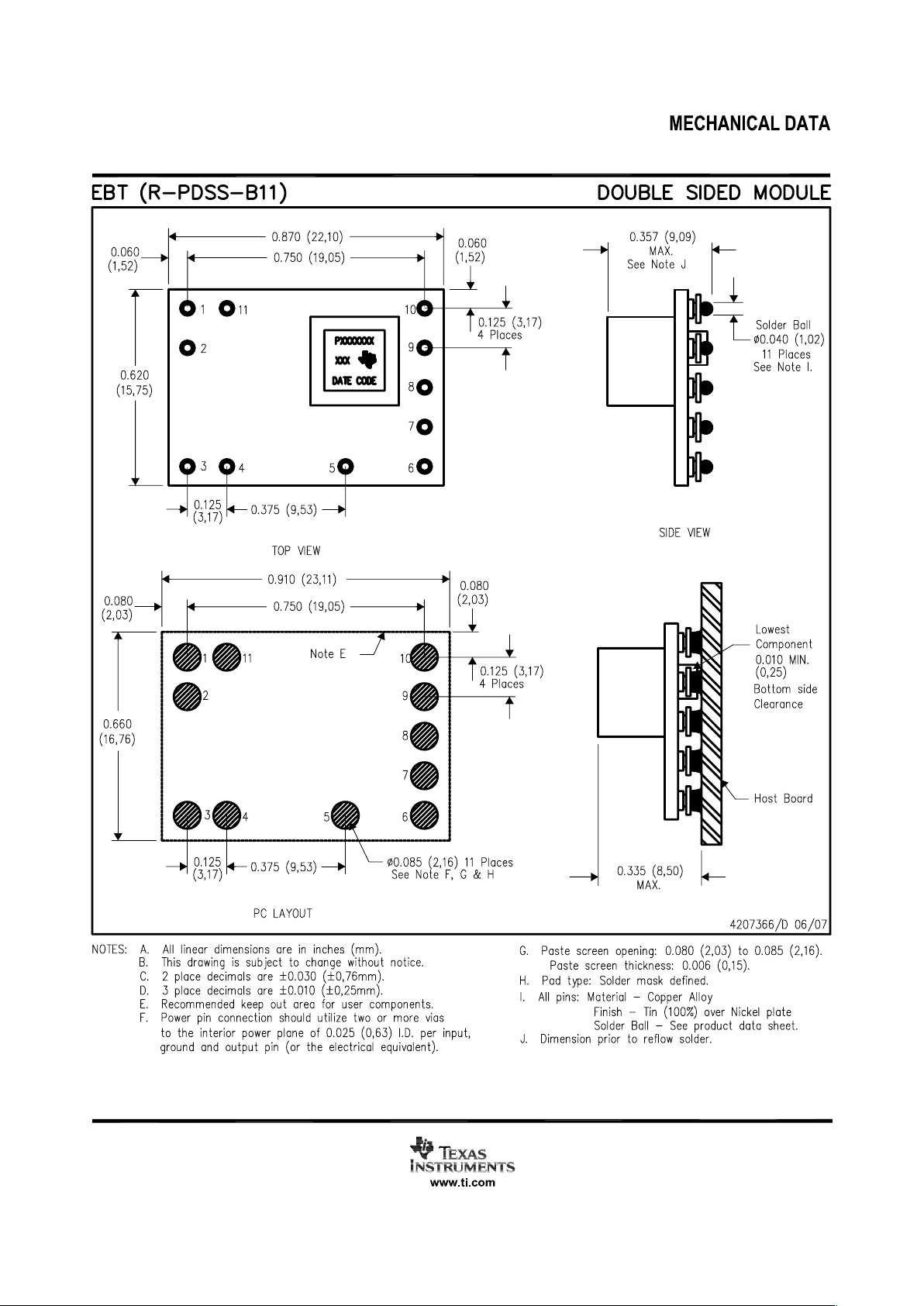
www.ti.com
FEATURES
APPLICATIONS
DESCRIPTION
PTH08T240F
SLTS277 – DECEMBER 2006
10-A, 4.5-V to 14-V INPUT, NON-ISOLATED
POWER MODULE FOR 3-GHz DSP SYSTEMS
• Up to 10-A Output Current • TurboTrans™ Technology
• 4.5-V to 14-V Input Voltage • Designed to meet Ultra-Fast Transient
Requirements for 3-GHz DSP Systems
• Wide-Output Voltage Adjust (0.69 V to 2.0 V)
• 15 mV Output Voltage Deviation
• ± 1.5% Total Output Voltage Variation
(C
O
= 3000 µ F, ∆ I = 5 A)
• Efficiencies up to 92%
• Output Overcurrent Protection
(Nonlatching, Auto-Reset)
• Wireless Infrastructure Base Stations
• Operating Temperature: –40 ° C to 85 ° C
• Safety Agency Approvals:
– UL/IEC/CSA-C22.2 60950-1
• Prebias Startup
• On/Off Inhibit
• Differential Output Voltage Remote Sense
• Adjustable Undervoltage Lockout
• Auto-Track™ Sequencing
• SmartSync Technology
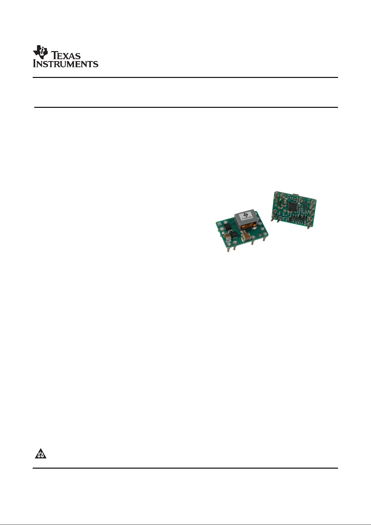
The PTH08T240F is a high-performance 10-A rated, non-isolated power module designed to meet ultra-fast
transient requirements for 3-GHz DSP systems. This module represent the 2nd generation of the popular PTH
series power modules which include a reduced footprint and additional features.
Operating from an input voltage range of 4.5 V to 14 V, the PTH08T240F requires a single resistor to set the
output voltage to any value over the range, 0.69 V to 2.0 V. The output voltage range makes the PTH08T240F
particularly suitable for the 3-GHz DSP's core voltage requirements between 0.9 V and 1.1 V. Additionally, the
wide input voltage range increases design flexibility by supporting operation with 5-V, 8-V, or 12-V intermediate
bus architectures.
The module incorporates a comprehensive list of features. Output over-current and over-temperature shutdown
protects against most load faults. A differential remote sense ensures tight load regulation. An adjustable
under-voltage lockout allows the turn-on voltage threshold to be customized. Auto-Track™sequencing is a
popular feature that greatly simplifies the simultaneous power-up and power-down of multiple modules in a
power system.
The PTH08T240F includes new patent pending technologies, TurboTrans™ and SmartSync. The TurboTrans
feature optimizes the transient response of the regulator while simultaneously reducing the quantity of external
output capacitors required to meet a target voltage deviation specification. TurboTrans allows PTH08T240F to
meet the tight transient voltage tolerances required by 3-GHz DSPs with minimal output capacitance. SmartSync
allows for switching frequency synchronization of multiple modules, thus simplifying EMI noise suppression tasks
and reducing input capacitor RMS current requirements. The module uses double-sided surface mount
construction to provide a low profile and compact footprint. Package options include both through-hole and
surface mount configurations that are lead (Pb) - free and RoHS compatible.
Please be aware that an important notice concerning availability, standard warranty, and use in critical applications of Texas
Instruments semiconductor products and disclaimers thereto appears at the end of this data sheet.
Auto-Track, TMS320 are trademarks of Texas Instruments.
PRODUCT PREVIEW information concerns products in the
Copyright © 2006, Texas Instruments Incorporated
formative or design phase of development. Characteristic data and
other specifications are design goals. Texas Instruments reserves
the right to change or discontinue these products without notice.
www.ti.com
PRODUCT PREVIEW
UDG−06005
R
TT
1%
0.05 W
(Optional)
C
O
1000 µF
(Required)
V
O
R
SET
[A]
1%
0.05 W
(Required)
C
I
330 µF
(Required)
R
UVLO
1%
0.05 W
(Optional)
VOAdj
TurboTranst
V
O
V
I
PTH08T240F
5
9
+
8
VI
Track
GND
TT
43
GND
GND
+Sense
6
L
O
A
D
−Sense
GND
+
Inhibit
INH/UVLO
Track
10
7
−Sense
+Sense
SYNC
1
SmartSync
2
11
CI2
22 µF
(Optional)
PTH08T240F
SLTS277 – DECEMBER 2006
These devices have limited built-in ESD protection. The leads should be shorted together or the device placed in conductive foam
during storage or handling to prevent electrostatic damage to the MOS gates.
A. R
SET
required to set the output voltage to a value higher than 0.69 V. See Electrical Characteristics table.
2
Submit Documentation Feedback
www.ti.com
DATASHEET TABLE OF CONTENTS
ENVIRONMENTAL AND ABSOLUTE MAXIMUM RATINGS
PTH08T240F
SLTS277 – DECEMBER 2006
ORDERING INFORMATION
For the most current package and ordering information, see the Package Option Addendum at the end of this datasheet, or see
the TI website at www.ti.com.
DATASHEET SECTION PAGE NUMBER
ENVIRONMENTAL AND ABSOLUTE MAXIMUM RATINGS 3
ELECTRICAL CHARACTERISTICS TABLE 4
TERMINAL FUNCTIONS 6
TYPICAL CHARACTERISTICS (VI= 12V) 7
TYPICAL CHARACTERISTICS (VI= 5V) 8
ADJUSTING THE OUTPUT VOLTAGE 9
INPUT & OUTPUT CAPACITOR RECOMMENDATIONS 11
TURBOTRANS™ INFORMATION 15
UNDERVOLTAGE LOCKOUT (UVLO) 20
SOFT-START POWER-UP 21
OUTPUT INHIBIT 22
OVER-CURRENT PROTECTION 23
OVER-TEMPERATURE PROTECTION 23
REMOTE SENSE 23
SYCHRONIZATION (SMARTSYNC) 24
AUTO-TRACK SEQUENCING 25
PREBIAS START-UP 28
TAPE & REEL AND TRAY DRAWINGS 30
(Voltages are with respect to GND)
UNIT
V
Track
Track pin voltage –0.3 to VI+ 0.3 V
T
A
Operating temperature range Over VIrange –40 to 85
suffix AH 235
Surface temperature of module body or
T
wave
Wave soldering temperature
pins for 5 seconds maximum.
suffix AD 260
° C
suffix AS 235
(1)
Surface temperature of module body or
T
reflow
Solder reflow temperature
pins
suffix AZ 260
(1)
T
stg
Storage temperature –40 to 125
(2)
Mechanical shock Per Mil-STD-883D, Method 2002.3 1 suffix AH & AD 500
msec, 1/2 sine, mounted
suffix AS & AZ 250 G
Mechanical vibration Mil-STD-883D, Method 2007.2 20-2000 Hz 15
Weight 5 grams
Flammability Meets UL94V-O
(1) During reflow of surface mount package version do not elevate peak temperature of the module, pins or internal components above the
stated maximum.
(2) The shipping tray or tape and reel cannot be used to bake parts at temperatures higher than 65°C.
3
Submit Documentation Feedback
www.ti.com
PRODUCT PREVIEW
ELECTRICAL CHARACTERISTICS
PTH08T240F
SLTS277 – DECEMBER 2006
PTH08T240F
TA= 25 ° C, VI= 5 V, VO= 1.0 V, CI= 330 µF, CO= 1000 µF, and IO= IOmax (unless otherwise stated)
PARAMETER TEST CONDITIONS PTH08T240F UNIT
MIN TYP MAX
I
O
Output current Over VOrange 25 ° C, natural convection 0 10 A
11 ×
0.69 ≤ VO≤ 1.2 4.5
V
O
(1)
V
I
Input voltage range Over IOrange V
1.2 < VO≤ 2.0 4.5 14
V
OADJ
Output voltage adjust range Over IOrange 0.69 2.0 V
Set-point voltage tolerance ± 0.5 ± 1
(2)
%V
o
Temperature variation –40 ° C < TA< 85 ° C ± 0.3 %V
o
V
O
Line regulaltion Over VIrange ± 3 mV
Load regulation Over IOrange ± 2 mV
Total output variation Includes set-point, line, load, –40 ° C ≤ TA≤ 85 ° C ± 1.5
(2)
%V
o
R
SET
= 4.78 k Ω , VO= 1.8 V 90%
R
SET
= 7.09 k Ω , VO= 1.5 V 88%
η Efficiency IO= 10 A
R
SET
= 12.1 k Ω , VO= 1.2 V 87%
R
SET
= 20.8 k Ω , VO= 1.0 V 85%
VORipple (peak-to-peak) 20-MHz bandwidth 10
(3)
mV
PP
I
LIM
Overcurrent threshold Reset, followed by auto-recovery 20 A
t
tr
Recovery time tbd µs
w/o TurboTrans
CO= 1000 µ F, Type C
∆ V
tr
2.5 A/µs load step VOover/undershoot tbd mV
Transient response 50 to 100% IOmax
t
trTT
w/ TurboTrans Recovery time tbd µs
VO= 2.5 V
CO= tbd µ F, Type C,
mV
∆ V
trTT
VOover/undershoot tbd
RTT = tbd Ω
I
IL
Track input current (pin 10) Pin to GND –130
(4)
µA
dV
track
/dt Track slew rate capability CO≤ CO(max) 1 V/ms
VIincreasing, R
UVLO
= OPEN 4.3 4.45
Adjustable Under-voltage lockout
UVLO
ADJ
VIdecreasing, R
UVLO
= OPEN 4.0 4.2 V
(pin 11)
Hysteresis, R
UVLO
≤ 52.3 k Ω 0.5
Input high voltage (VIH) Open
(5)
V
Inhibit control (pin 11) Input low voltage (VIL) -0.2 0.8
Input low current (IIL), Pin 11 to GND -235 µA
I
in
Input standby current Inhibit (pin 11) to GND, Track (pin 10) open 5 mA
f
s
Switching frequency Over VIand IOranges, SmartSync (pin 1) to GND 260 300 340 kHz
Synchronization (SYNC)
f
SYNC
240 400 kHz
frequency
V
SYNCH
SYNC High-Level Input Voltage 2 5.5 V
V
SYNCL
SYNC Low-Level Input Voltage 0.8 V
t
SYNC
SYNC Minimum Pulse Width 200 nSec
Nonceramic 330
(6)
C
I
External input capacitance µF
Ceramic 22
(6)
(1) The maximum input voltage is duty cycle limited to (VO× 11) or 14 volts, whichever is less. The maximum allowable input voltage is a
function of switching frequency, and may increase or decrease when the SmartSync feature is utilized. Please review the SmartSync
section of the Application Information for further guidance.
(2) The set-point voltage tolerance is affected by the tolerance and stability of R
SET
. The stated limit is unconditionally met if R
SET
has a
tolerance of 1% with 100 ppm/°C or better temperature stability.
(3) For output voltages less than 1.7 V, the ripple may increase (up to 2 × ) when operating at input voltages greater than (VO× 11). See the
SmartSync section of the Application Information for input voltage and frequency limitations.
(4) A low-leakage (<100 nA), open-drain device, such as MOSFET or voltage supervisor IC, is recommended to control pin 10. The
open-circuit voltage is less than 8 Vdc.
(5) This control pin has an internal pull-up. Do not place an external pull-up on this pin. If it is left open-circuit, the module operates when
input power is applied. A small, low-leakage (<100 nA) MOSFET is recommended for control. For additional information, see the related
application information section.
(6) A 330 µF electrolytic input capacitor is required for proper operation. The electrolytic capacitor must be rated for a minimum of 500 mA
rms of ripple current.
4
Submit Documentation Feedback

www.ti.com
PTH08T240F
SLTS277 – DECEMBER 2006
ELECTRICAL CHARACTERISTICS (continued)
PTH08T240F
TA= 25 ° C, VI= 5 V, VO= 1.0 V, CI= 330 µF, CO= 1000 µF, and IO= IOmax (unless otherwise stated)
PARAMETER TEST CONDITIONS PTH08T240F UNIT
MIN TYP MAX
Nonceramic 1000
(7)
5000
(8)
Capacitance Value µF
w/o TurboTrans Ceramic 500
Equivalent series resistance (non-ceramic) 7 m Ω
C
O
External output capacitance
see table
Capacitance Value µF
(7) (9)
w/ TurboTrans
Capacitance × ESR product (CO× ESR) 1000 10000
(9)
µF × m Ω
Per Telcordia SR-332, 50% stress,
MTBF Reliability 6.1
106Hr
TA= 40 ° C, ground benign
(7) 1000 µF of external output capacitance is required for basic operation. The minimum output capacitance requirement increases when
TurboTrans™ (TT) technology is utilized. See related Application Information for more guidance.
(8) This is the calculated maximum disregarding TurboTrans™ technology. When the TurboTrans™ feature is utilized, the minimum output
capacitance must be increased.
(9) When using TurboTrans™ technology, a minimum value of output capacitance is required for proper operation. Additionally, low ESR
capacitors are required for proper operation. See the application notes for further guidance.
5
Submit Documentation Feedback

www.ti.com
PRODUCT PREVIEW
1 10
9
8
7
6
543
2
11
PTH08T240F
(Top View)
PTH08T240F
SLTS277 – DECEMBER 2006
TERMINAL FUNCTIONS
TERMINAL
DESCRIPTION
NAME NO.
V
I
2 The positive input voltage power node to the module, which is referenced to common GND.
V
O
5 The regulated positive power output with respect to GND.
This is the common ground connection for the VIand VOpower connections. It is also the 0 Vdcreference for
GND 3, 4
the control inputs.
The Inhibit pin is an open-collector/drain, negative logic input that is referenced to GND. Applying a low level
ground signal to this input disables the module’s output and turns off the output voltage. When the Inhibit control
is active, the input current drawn by the regulator is significantly reduced. If the Inhibit pin is left open-circuit, the
Inhibit
(1)
and
module produces an output whenever a valid input source is applied.
11
UVLO
This pin is also used for input undervoltage lockout (UVLO) programming. Connecting a resistor from this pin to
GND (pin 3) allows the ON threshold of the UVLO to be adjusted higher than the default value. For more
information, see the Application Information section.
A 0.05 W 1% resistor must be directly connected between this pin and pin 7 (–Sense) to set the output voltage
to a value higher than 0.69 V. The temperature stability of the resistor should be 100 ppm/ ° C (or better). The
setpoint range for the output voltage is from 0.69 V to 2.0 V. If left open circuit, the output voltage will default to
VoAdjust 8
its lowest value. For further information, on output voltage adjustment see the related application note.
The specification table gives the preferred resistor values for a number of standard output voltages.
The sense input allows the regulation circuit to compensate for voltage drop between the module and the load.
+ Sense 6
For optimal voltage accuracy, +Sense must be connected to VO, very close to the load.
The sense input allows the regulation circuit to compensate for voltage drop between the module and the load.
– Sense 7 For optimal voltage accuracy –Sense must be connected to GND (pin 4) very close to the module (within
10 cm).
This is an analog control input that enables the output voltage to follow an external voltage. This pin becomes
active typically 20 ms after the input voltage has been applied, and allows direct control of the output voltage
from 0 V up to the nominal set-point voltage. Within this range the module's output voltage follows the voltage at
Track 10
the Track pin on a volt-for-volt basis. When the control voltage is raised above this range, the module regulates
at its set-point voltage. The feature allows the output voltage to rise simultaneously with other modules powered
from the same input bus. If unused, this input should be connected to VI.
NOTE: Due to the undervoltage lockout feature, the output of the module cannot follow its own input voltage
during power up. For more information, see the related application note.
This input pin adjusts the transient response of the regulator. To activate the TurboTrans™ feature, a 1%,
50 mW resistor must be connected between this pin and pin 6 (+Sense) very close to the module. For a given
value of output capacitance, a reduction in peak output voltage deviation is achieved by utililizing this feature. If
TurboTrans™ 9
unused, this pin must be left open-circuit. The resistance requirement can be selected from the TurboTrans™
resistor table in the Application Information section. External capacitance must never be connected to this pin
unless the TurboTrans resistor value is a short, 0 Ω .
This input pin sychronizes the switching frequency of the module to an external clock frequency. The SmartSync
feature can be used to sychronize the switching fequency of multiple PTH08T240F modules, aiding EMI noise
SmartSync 1
suppression efforts. If unused, this pin should be connected to GND (pin 3). For more information, please review
the Application Information section.
(1) Denotes negative logic: Open = Normal operation, Ground = Function active
6
Submit Documentation Feedback
www.ti.com
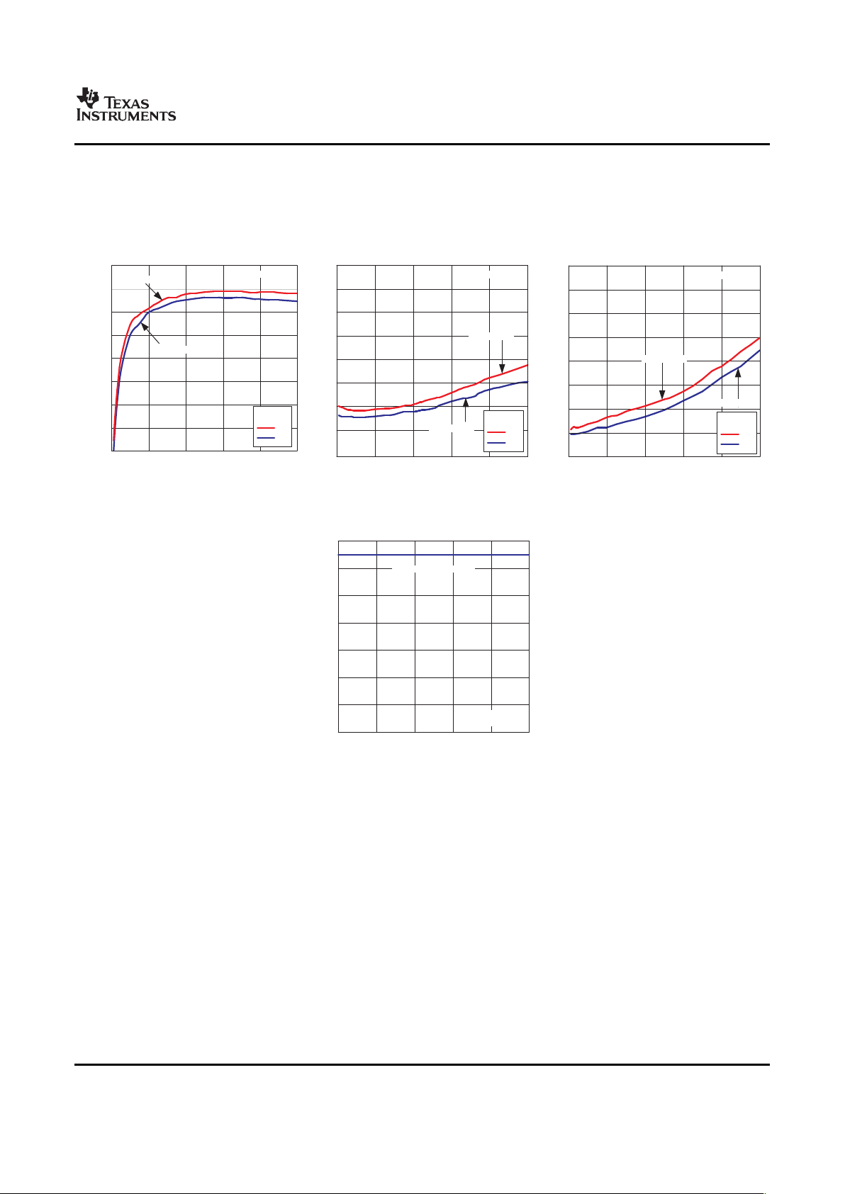
TYPICAL CHARACTERISTICS
(1) (2)
CHARACTERISTIC DATA (V
I
= 12 V)
0
20
2 4 6 8 10
40
30
50
60
70
90
80
100
IO − Output Current − A
V
I
= 12 V
V
O
= 1.8 V
V
O
= 1.2 V
η − Efficiency − %
V
O
(V)
1.8
1.2
0 2 4 6 8 10
0
0.5
1.0
2.5
2.0
3.0
4.0
3.5
1.5
IO − Output Current − A
V
I
= 12 V
V
O
= 1.8 V
V
O
= 1.2 V
P
D
− Power Dissipation − W
V
O
(V)
1.8
1.2
6 8 10
12
16
14
0
0
2 4
2
4
8
6
10
IO − Output Current − A
V
I
= 12 V
V
O
− Output Voltage Ripple − mV
PP
V
O
= 1.2 V
V
O
= 1.8 V
V
O
(V)
1.8
1.2
IO − Output Current − A
T
A
− Ambient Temperature − °C
0 2 4 6 8 10
20
40
30
50
70
60
90
80
V
I
= 12 V
V
O
= 1.2 V
Natural Convection
PTH08T240F
SLTS277 – DECEMBER 2006
EFFICIENCY OUTPUT RIPPLE POWER DISSIPATION
vs vs vs
LOAD CURRENT LOAD CURRENT LOAD CURRENT
Figure 1. Figure 2. Figure 3.
SAFE OPERATING AREA
Figure 4.
(1) The electrical characteristic data has been developed from actual products tested at 25°C. This data is considered typical for the
converter. Applies to Figure 1 , Figure 2 , and Figure 3 .
(2) The temperature derating curves represent the conditions at which internal components are at or below the manufacturer's maximum
operating temperatures. Derating limits apply to modules soldered directly to a 100 mm x 100 mm double-sided PCB with 2 oz. copper.
For surface mount packages (AS and AZ suffix), multiple vias must be utilized. Please refer to the mechanical specification for more
information. Applies to Figure 4 .
7
Submit Documentation Feedback

www.ti.com
PRODUCT PREVIEW
TYPICAL CHARACTERISTICS
(1) (2)
CHARACTERISTIC DATA (V
I
= 5 V)
0 2 4 6 8 10
0
0.5
1.0
2.0
1.5
2.5
IO − Output Current − A
V
I
= 5 V
V
O
= 0.9 V
V
O
= 1.8 V
P
D
− Power Dissipation − W
V
O
= 1.2 V
V
O
= 0.7 V
0.7
0.9
1.8
1.2
V
O
(V)
IO − Output Current − A
V
O
− Output Voltage Ripple − mV
PP
0
0
2 4 6 8 10
2
6
4
10
8
V
I
= 5 V
V
O
= 1.8 V
V
O
= 1.2 V
V
O
= 0.9 V
V
O
= 0.7 V
0.7
0.9
1.8
1.2
V
O
(V)
0
40
2 4 6 8 10
50
60
70
80
90
100
30
0.7
0.9
1.8
1.2
IO − Output Current − A
V
I
= 5 V
V
O
= 1.8 V
V
O
= 1.2 V
η − Efficiency − %
V
O
= 0.9 V
V
O
= 0.7 V
V
O
(V)
0 2 4 6 8 10
20
40
30
50
70
60
90
80
Natural
Convection
IO − Output Current − A
V
I
= 5 V
All V
O
T
A
− Ambient Temperature − °C
PTH08T240F
SLTS277 – DECEMBER 2006
EFFICIENCY OUTPUT RIPPLE POWER DISSIPATION
vs vs vs
LOAD CURRENT LOAD CURRENT LOAD CURRENT
Figure 5. Figure 6. Figure 7.
SAFE OPERATING AREA
Figure 8.
(1) The electrical characteristic data has been developed from actual products tested at 25°C. This data is considered typical for the
converter. Applies to Figure 5 , Figure 6 , and Figure 7 .
(2) The temperature derating curves represent the conditions at which internal components are at or below the manufacturer's maximum
operating temperatures. Derating limits apply to modules soldered directly to a 100 mm x 100 mm double-sided PCB with 2 oz. copper.
For surface mount packages (AS and AZ suffix), multiple vias must be utilized. Please refer to the mechanical specification for more
information. Applies to Figure 8 .
8
Submit Documentation Feedback

www.ti.com
APPLICATION INFORMATION
ADJUSTING THE OUTPUT VOLTAGE
R =10k x
SET
W
0.69
V -0.69
O
-1.43kW
(1)
+Sense
−Sense
VoAdjGND
PTH08T240F
3
5
6
7
8
+Sense
−Sense
GND
4
GND
+
V
O
V
O
R
SET
1%
0.05 W
UDG−06077
C
O
PTH08T240F
SLTS277 – DECEMBER 2006
The VoAdjust control (pin 8) sets the output voltage of the PTH08T240F. The adjustment range is 0.69 V to 2.0
V. The adjustment method requires the addition of a single external resistor, R
SET
, that must be connected
directly between the V
O
Adjust and – Sense pins. Table 1 gives the standard value of the external resistor for a
number of standard voltages, along with the actual output voltage that this resistance value provides.
For other output voltages, the value of the required resistor can either be calculated using the following formula,
or simply selected from the range of values given in Table 2 . Figure 9 shows the placement of the required
resistor.
Table 1. Standard Values of R
SET
for Standard Output Voltages
VO(Standard) (V) R
SET
(Standard Value) (k Ω ) VO(Actual) (V)
1.8 4.75 1.807
1.5 6.98 1.510
1.2
(1)
12.1 1.200
1
(1)
20.5 1.004
0.7
(1)
681 0.700
(1) The maximum input voltage is (VO× 11) or 14 V, whichever is less. The maximum allowable input
voltage is a function of switching frequency and may increase or decrease when the Smart Sync
feature is utilized. Please review the Smart Sync application section for further guidance.
(1) R
SET
: Use a 0.05 W resistor with a tolerance of 1% and temperature stability of 100 ppm/ ° C (or better). Connect the
resistor directly between pins 8 and 7, as close to the regulator as possible, using dedicated PCB traces.
(2) Never connect capacitors from VOAdjust to either + Sense, GND, or VO. Any capacitance added to the VOAdjust pin
affects the stability of the regulator.
Figure 9. V
O
Adjust Resistor Placement
9
Submit Documentation Feedback

www.ti.com
PRODUCT PREVIEW
PTH08T240F
SLTS277 – DECEMBER 2006
Table 2. Output Voltage Set-Point Resistor Values
(Standard Values)
VORequired (V) R
SET
(k Ω )
0.70
(1)
681
0.75
(1)
113
0.80
(1)
61.9
0.85
(1)
41.2
0.90
(1)
31.6
0.95
(1)
24.9
1.00
(1)
20.5
1.05
(1)
17.8
1.10
(1)
15.4
1.15
(1)
13.3
1.20
(1)
12.1
1.25
(1)
10.7
1.30 9.88
1.35 9.09
1.40 8.25
1.45 7.68
1.50 6.98
1.55 6.49
1.60 6.04
1.65 5.76
1.70 5.36
1.75 5.11
1.80 4.75
1.85 4.53
1.90 4.22
1.95 4.02
2.00 3.83
(1) The maximum input voltage is (VO× 11) or 14 V, whichever is less.
The maximum allowable input voltage is a function of switching
frequency and may increase or decrease when the Smart Sync
feature is utilized. Please review the Smart Sync application section
for further guidance.
10
Submit Documentation Feedback

www.ti.com
TurboTrans™ Technology
TurboTrans™ Selection
PTH08T240F
SLTS277 – DECEMBER 2006
TurboTrans technology is a feature introduced in the T2 generation of the PTH/PTV family of power modules.
TurboTrans optimizes the transient response of the regulator with added external capacitance using a single
external resistor. Benefits of this technology include reduced output capacitance, minimized output voltage
deviation following a load transient, and enhanced stability when using ultra-low ESR output capacitors. The
amount of output capacitance required to meet a target output voltage deviation will be reduced with TurboTrans
activated. Likewise, for a given amount of output capacitance, with TurboTrans engaged, the amplitude of the
voltage deviation following a load transient will be reduced. Applications requiring tight transient voltage
tolerances and minimized capacitor footprint area will benefit greatly from this technology.
Utilizing TurboTrans requires connecting a resistor, R
TT
, between the +Sense pin (pin 6) and the TurboTrans pin
(pin 9). The value of the resistor directly corresponds to the amount of output capacitance required. All T2
products require a minimum value of output capacitance whether or not TurboTrans is utilized. For the
PTH08T240F, the minimum required capacitance is 1000 µ F. When using TurboTrans, capacitors with a
capacitance × ESR product below 10,000 µ F × m Ω are required. (Multiply the capacitance (in µ F) by the ESR (in
m Ω ) to determine the capacitance × ESR product.) See the Capacitor Selection section of the datasheet for a
variety of capacitors that meet this criteria.
Figure 10 shows the amount of output capacitance required to meet a desired transient voltage deviation with
and without TurboTrans for Type C (e.g. OS-CON) capacitors; Type B (e.g. polymer-tantalum) capacitor charts
will be added. To calculate the proper value of R
TT
, first determine your required transient voltage deviation limits
and magnitude of your transient load step. Next, determine what type of output capacitors will be used. (If more
than one type of output capacitor is used, select the capacitor type that makes up the majority of your total
output capacitance.) Knowing this information, use the chart (Figure 10 ; for Type C capacitors) that corresponds
to the capacitor type selected. To use the chart, begin by dividing the maximum voltage deviation limit (in mV)
by the magnitude of your load step (in Amps). This gives a mV/A value. Find this value on the Y-axis of the
appropriate chart. Read across the graph to the 'With TurboTrans' plot. From this point, read down to the X-axis
which lists the minimum required capacitance, CO, to meet that transient voltage deviation. The required R
TT
resistor value can then be calculated using the equation or selected from the TurboTrans table. The TurboTrans
tables include both the required output capacitance and the corresponding R
TT
values to meet several values of
transient voltage deviation for 25% (2.5 A), 50% (5 A), and 75% (7.5 A) output load steps.
The chart can also be used to determine the achievable transient voltage deviation for a given amount of output
capacitance. By selecting the amount of output capacitance along the X-axis, reading up to the desired 'With
TurboTrans'' curve, and then over to the Y-axis, gives the transient voltage deviation limit for that value of output
capacitance. The required R
TT
resistor value can be calculated using the equation or selected from the
TurboTrans table.
As an example, let's look at a 5-V application requiring a 15 mV deviation during an 5 A, 50% load transient. A
majority of 680 µ F, 10 m Ω ouput capacitors will be used. Use the 5-V, Type C capacitor chart, Figure 10 .
Dividing 15 mV by 5 A gives 3 mV/A transient voltage deviation per amp of transient load step. Select 3 mV/A on
the Y-axis and read across to the 'With TurboTrans'' plot. Following this point down to the X-axis gives a
minimum required output capacitance of approximately 3000 µ F. The required R
TT
resistor value for 3000 µ F
can then be calculated or selected from Table 3 . The required R
TT
resistor is approximately 13.0 k Ω .
11
Submit Documentation Feedback

www.ti.com
PRODUCT PREVIEW
PTH08T240F Type C Capacitors
6000
5000
4000
3000
2000
1000
10
7
6
5
4
3
2
1
10000
8000
9000
7000
9
8
C − Capacitance − µF
Transient −mV/A
Without TurboTrans
With TurboTrans
R
TT
+
40 ƪ1 *ǒCOń6300
Ǔƫ
ƪ
ǒ
ǒ
ǒ
5 C
O
Ǔ
) 1300
Ǔ
ń6300Ǔ* 1
ƫ
(kW)
(2)
PTH08T240F
SLTS277 – DECEMBER 2006
5-V Input
Figure 10. Capacitor Type C, 5000 < C( µ F) × ESR(m Ω ) ≤
10,000 (e.g. OS-CON)
Table 3. Type C TurboTrans C
O
Values and Required R
TT
Selection Table
Transient Voltage Deviation (mV) 5-V Input
25% load step 50% load step 75% load step C
O
R
TT
(2.5 A) (5 A) (7.5 A) Minimum Required Required TurboTrans
Output Resistor (k Ω )
Capacitance ( µ F)
23 45 68 1000 open
20 40 60 1150 274
18 35 53 1300 133
15 30 45 1500 76.8
13 25 38 1810 44.2
10 20 30 2300 24.9
8 15 23 3050 12.7
5 10 15 4620 3.74
R
TT
Resistor Selection
The TurboTrans resistor value, R
TT
can be determined from the TurboTrans programming, see Equation 2 .
Where C
O
is the total output capacitance in µ F. C
O
values greater than or equal to 6300 µ F require R
TT
to be a
short, 0 Ω . (R
TT
results in a negative value when C
O
> 6300 µ F).
To ensure stability, the value of R
TT
must be calculated using the minimum required output capacitance
determined from the capacitor transient response charts above.
12
Submit Documentation Feedback


IMPORTANT NOTICE
Texas Instruments Incorporated and its subsidiaries (TI) reserve the right to make corrections, modifications, enhancements,
improvements, and other changes to its products and services at any time and to discontinue any product or service without notice.
Customers should obtain the latest relevant information before placing orders and should verify that such information is current and
complete. All products are sold subject to TI’s terms and conditions of sale supplied at the time of order acknowledgment.
TI warrants performance of its hardware products to the specifications applicable at the time of sale in accordance with TI’s
standard warranty. Testing and other quality control techniques are used to the extent TI deems necessary to support this
warranty. Except where mandated by government requirements, testing of all parameters of each product is not necessarily
performed.
TI assumes no liability for applications assistance or customer product design. Customers are responsible for their products and
applications using TI components. To minimize the risks associated with customer products and applications, customers should
provide adequate design and operating safeguards.
TI does not warrant or represent that any license, either express or implied, is granted under any TI patent right, copyright, mask
work right, or other TI intellectual property right relating to any combination, machine, or process in which TI products or services
are used. Information published by TI regarding third-party products or services does not constitute a license from TI to use such
products or services or a warranty or endorsement thereof. Use of such information may require a license from a third party under
the patents or other intellectual property of the third party, or a license from TI under the patents or other intellectual property of TI.
Reproduction of TI information in TI data books or data sheets is permissible only if reproduction is without alteration and is
accompanied by all associated warranties, conditions, limitations, and notices. Reproduction of this information with alteration is an
unfair and deceptive business practice. TI is not responsible or liable for such altered documentation. Information of third parties
may be subject to additional restrictions.
Resale of TI products or services with statements different from or beyond the parameters stated by TI for that product or service
voids all express and any implied warranties for the associated TI product or service and is an unfair and deceptive business
practice. TI is not responsible or liable for any such statements.
TI products are not authorized for use in safety-critical applications (such as life support) where a failure of the TI product would
reasonably be expected to cause severe personal injury or death, unless officers of the parties have executed an agreement
specifically governing such use. Buyers represent that they have all necessary expertise in the safety and regulatory ramifications
of their applications, and acknowledge and agree that they are solely responsible for all legal, regulatory and safety-related
requirements concerning their products and any use of TI products in such safety-critical applications, notwithstanding any
applications-related information or support that may be provided by TI. Further, Buyers must fully indemnify TI and its
representatives against any damages arising out of the use of TI products in such safety-critical applications.
TI products are neither designed nor intended for use in military/aerospace applications or environments unless the TI products are
specifically designated by TI as military-grade or "enhanced plastic." Only products designated by TI as military-grade meet military
specifications. Buyers acknowledge and agree that any such use of TI products which TI has not designated as military-grade is
solely at the Buyer's risk, and that they are solely responsible for compliance with all legal and regulatory requirements in
connection with such use.
TI products are neither designed nor intended for use in automotive applications or environments unless the specific TI products
are designated by TI as compliant with ISO/TS 16949 requirements. Buyers acknowledge and agree that, if they use any
non-designated products in automotive applications, TI will not be responsible for any failure to meet such requirements.
Following are URLs where you can obtain information on other Texas Instruments products and application solutions:
Products Applications
Amplifiers amplifier.ti.com Audio www.ti.com/audio
Data Converters dataconverter.ti.com Automotive www.ti.com/automotive
DSP dsp.ti.com Broadband www.ti.com/broadband
Interface interface.ti.com Digital Control www.ti.com/digitalcontrol
Logic logic.ti.com Military www.ti.com/military
Power Mgmt power.ti.com Optical Networking www.ti.com/opticalnetwork
Microcontrollers microcontroller.ti.com Security www.ti.com/security
RFID www.ti-rfid.com Telephony www.ti.com/telephony
Low Power www.ti.com/lpw Video & Imaging www.ti.com/video
Wireless
Wireless www.ti.com/wireless
Mailing Address: Texas Instruments, Post Office Box 655303, Dallas, Texas 75265
Copyright © 2007, Texas Instruments Incorporated
 Loading...