

Page 1
查询PTH08T210W供应商
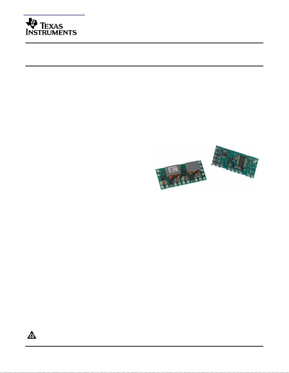
PTH08T210W
www.ti.com
SLTS262B–OCTOBER 2005 – REVISED NOVEMBER 2005
30-A, 5.5-V to 14-V INPUT, NON-ISOLATED,
WIDE OUTPUT ADJUST, POWER MODULE w/TurboTrans™
FEATURES
• Up to 30-A Output Current • TurboTrans™ Technology
• 5.5-V to 14-V Input Voltage • Designed to meet Ultra-Fast Transient
• Wide-Output Voltage Adjust (0.7 V to 3.6 V)
• Efficiencies up to 96%
•±1.5% Total Output Voltage Variation
• On/Off Inhibit
• Differential Output Voltage Remote Sense
• Adjustable Undervoltage Lockout
• Output Overcurrent Protection
(Nonlatching, Auto-Reset)
• Operating Temperature: –40°Cto85°C
• Safety Agency Approvals:
– UL 1950, CSA 22.2 950, EN60950 VDE
(Pending)
Requirements up to 300 A/µs
• Auto-Track™ Sequencing
• Multi-Phase, Switch-Mode Topology
APPLICATIONS
• Complex Multi-Voltage Systems
• Microprocessors
• Bus Drivers
DESCRIPTION
The PTH08T210W is a high-performance 30-A rated, non-isolated power module which utilizes a multi-phase,
switch-mode topology. This module represents the 2nd generation of the PTH series power modules which
include a reduced footprint and improved features.
Operating from an input voltage range of 5.5 V to 14 V, the PTH08T210W requires a single resistor to set the
output voltage to any value over the range, 0.7 V to 3.6 V. The wide input voltage range makes the
PTH08T210W particularly suitable for advanced computing and server applications that uses a loosely regulated
8-V to 12-V intermediate distribution bus. The module uses double-sided surface mount construction to provide a
low profile and compact footprint. Package options include both through-hole and surface mount configurations
that are lead (Pb) – free and RoHS compatible.
A new feature included in this 2nd generation of PTH and PTV modules is TurboTrans™ technology (patent
pending). TurboTrans allows the transient response of the regulator to be optimized externally, resulting in a
reduction of output voltage deviation following a load transient and a reduction in required output capacitance.
This feature also offers enhanced stability when used with ultra-low ESR output capacitors.
The PTH08T210W incorporates a comprehensive list of standard features. They include on/off inhibit, a
differential remote output voltage sense which ensures tight load regulation, and an output overcurrent and
overtemperature shutdown to protect against load faults. A programmable undervoltage lockout allows the
turn-on voltage threshold to be customized. AutoTrack™ sequencing is a feature which simplifies the
simultaneous power-up and power-down of multiple modules in a power system by allowing the outputs to track
a common voltage.
Please be aware that an important notice concerning availability, standard warranty, and use in critical applications of Texas
Instruments semiconductor products and disclaimers thereto appears at the end of this data sheet.
TurboTrans, AutoTrack, TMS320 are trademarks of Texas Instruments.
PRODUCTION DATA information is current as of publication date.
Products conform to specifications per the terms of the Texas
Instruments standard warranty. Production processing does not
necessarily include testing of all parameters.
Copyright © 2005, Texas Instruments Incorporated
Page 2
www.ti.com
PTH08T210W
SLTS262B–OCTOBER 2005 – REVISED NOVEMBER 2005
These devices have limited built-in ESD protection. The leads should be shorted together or the device placed in conductive foam
during storage or handling to prevent electrostatic damage to the MOS gates.
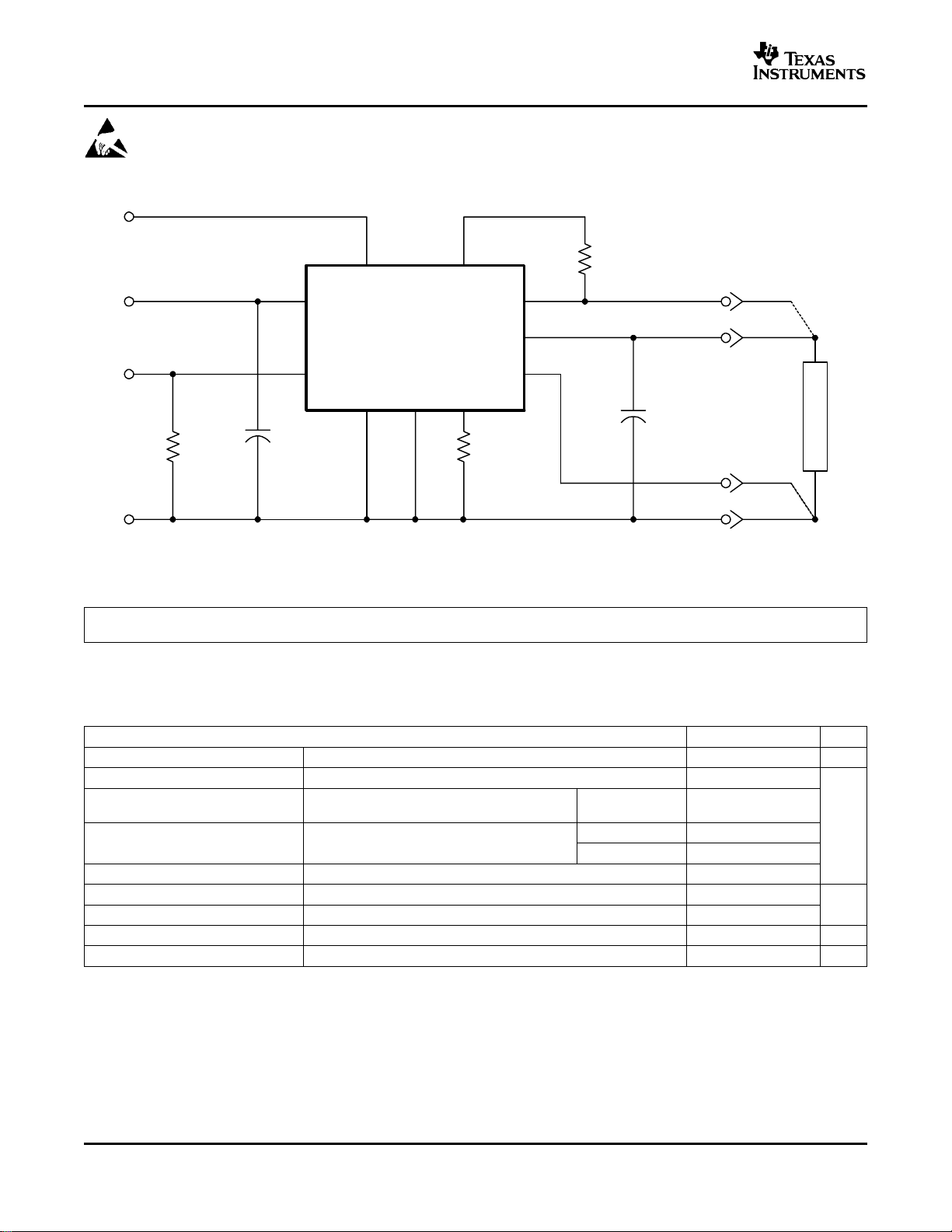
Track
14
TurboTranst
13
R
1%
TT
0.05 W
VI
Inhibit
GND
A. R
2,6
Track
V
I
PTH08T210W
1
INH/UVLO
+
R
UVLO
1%
0.05 W
(Opional)
is required to set the output voltage higher than 0.7 V. See the Electrical Characteristics table.
SET
C
I
470 µF
(Required)
GND
GND
7,83,4
TT
VOAdj
12
+Sense
V
O
−Sense
R
SET
1%
0.05 W
(Required)
10
5, 9
11
(Optional)
+
C
O
470 µF
(Required)
+Sense
V
O
−Sense
GND
UDG−05097
L
O
A
D
ORDERING INFORMATION
For the most current package and ordering information, see the Package Option Addendum at the end of this datasheet, or see
the TI website at www.ti.com.
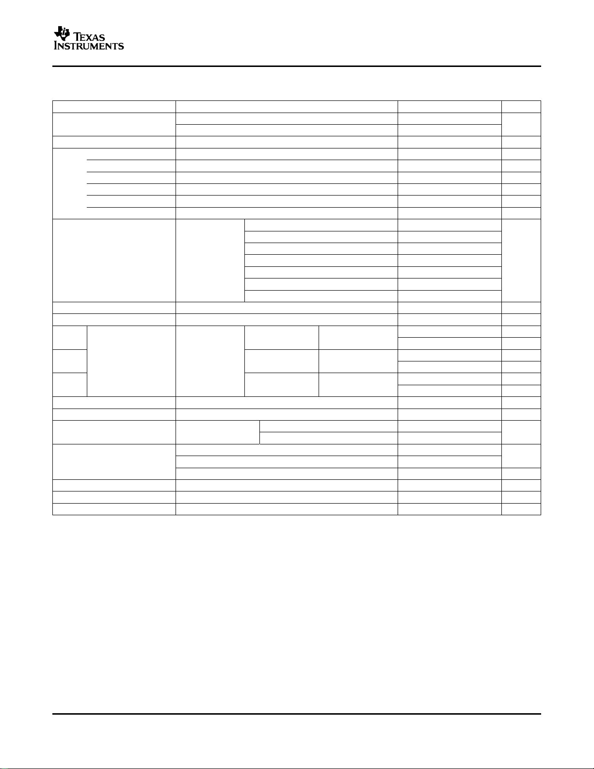
ENVIRONMENTAL AND ABSOLUTE MAXIMUM RATINGS
(Voltages are with respect to GND)
UNIT UNIT
Signal input voltage Track control (pin 14) –0.3 to VI+0.3 V
T
T
T
T
(1) During reflow of surface mount package version do not elevate peak temperature of the module, pins or internal components above the
Operating temperature range Over VIrange –40 to 85
A
Wave soldering temperature PTH08T210WAD 260
wave
Solder reflow temperature
reflow
Storage temperature –40 to 125
stg
Surface temperature of module body or pins
(20 seconds)
Surface temperature of module body or pins
(20 seconds)
PTH08T210WAS 235
PTH08T210WAZ 260
(1)
(1)
Mechanical shock Per Mil-STD-883D, Method 2002.3 1 msec, ½ sine, mounted 250
Mechanical vibration Mil-STD-883D, Method 2007.2 20-2000 Hz 15
Weight 8.5 grams
Flammability Meets UL94V-O
stated maximum.
°C
G
2
Submit Documentation Feedback
Page 3
PTH08T210W
www.ti.com
SLTS262B–OCTOBER 2005 – REVISED NOVEMBER 2005
ELECTRICAL CHARACTERISTICS
TA=25°C, VI=12V,VO= 3.3 V, CI= 470 µF, CO= 470 µF OS-CON, and IO=IOmax (unless otherwise stated)
PARAMETER TEST CONDITIONS MIN TYP MAX UNIT
I
O
V
I
Output current A
Input voltage range Over IOrange 5.5 14 V
Output adjust range Over I
range 0.7 3.6 V
O
Set-point voltage tolerance ±1
V
O
Temperature variation –40°C<TA<85°C ±0.3 %V
Line regulation Over VIrange ±4mV
Load regulation Over I
range ±7mV
O
Total output variation Includes set-point, line, load, –40°C ≤ T
V
=5.5Vto14V
η Efficiency R
Ripple (peak-to-peak) 20-MHz bandwidth 25 mV
V
O
I
LIM
t
tr
∆V
t
tr
∆V
t
trTT
∆V
I
IL
dV
UVLO
Overcurrent threshold Reset, followed by auto-recovery 55 A
tr
Transient response
tr
trTT
Track input current (pin 14) Pin to GND –130
/dt Track slew rate capability CO≤ CO(max) 1V/ms
track
Adjustable Undervoltage
ADJ
lockout (pin 1)
Inhibit control (pin 1) Input low voltage (V
I
in
f
s
C
I
Input standby current Inhibit (pin 1) to GND, Track (pin 14) open 3 mA
Switching frequency Over VIand IOranges 480 kHz
External input capacitance 470
I
I
=26A
O
w/o TurboTrans Recovery time 50 µs
=470 µF
C
O
1 A/µs load step
50 to 100% IOmax
w/o TurboTrans Recovery time 50 µs
C
=940 µF, Type C
O
w/ TurboTrans Recovery time 50 µs
=940 µF, Type C
C
O
Pin 1 open V
Input high voltage (V
Input low current (I
)V
IH
)-0.20.6
IL
)125µA
IL
(1) The set-point voltage tolerance is affected by the tolerance and stability of R
tolerance of 1% with 100 ppm/°C or better temperature stability.
(2) A low-leakage (<100 nA), open-drain device, such as MOSFET or voltage supervisor IC, is recommended to control pin 14. The
open-circuit voltage is less than 8 Vdc.
(3) This control pin has an internal pullup to the input voltage VI. If it is left open-circuit, the module operates when input power is applied. A
small, low-leakage (<100 nA) MOSFET is recommended for control. For additional information, see the related application note.
(4) A 470 µF electrolytic input capacitor is required for proper operation. The capacitor must be rated for a minimum of 500 mA rms of ripple
current.
25°C, natural convection 0 25
60°C, 200 LFM 0 30
≤ 85°C ±1.5
A
R
=1.62kΩ,VO= 3.3 V 93%
SET
=5.23kΩ,VO= 2.5 V 91%
R
SET
= 12.7 kΩ,VO= 1.8 V 89%
R
SET
= 19.6 kΩ,VO= 1.5 V 89%
SET
R
= 35.7 kΩ,VO= 1.2 V 87%
SET
= 63.4 kΩ,VO= 1.0 V 84%
R
SET
Open, V
= 0.7 V 80%
O
VOover/undershoot 150 mV
VOover/undershoot 125 mV
VOover/undershoot 85 mV
increasing 5 5.5
V
I
V
decreasing 4.1
I
– 0.5 Open
I
(4)
. The stated limit is unconditionally met if R
SET
(1)
(1)
(2)
(3)
SET
%V
%V
has a
o
o
o
PP
µA
V
µF
Submit Documentation Feedback
3
Page 4
www.ti.com
PTH08T210W
SLTS262B–OCTOBER 2005 – REVISED NOVEMBER 2005
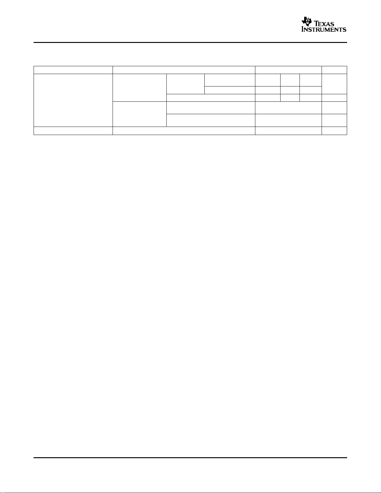
ELECTRICAL CHARACTERISTICS (continued)
TA=25°C, VI=12V,VO= 3.3 V, CI= 470 µF, CO= 470 µF OS-CON, and IO=IOmax (unless otherwise stated)
PARAMETER TEST CONDITIONS MIN TYP MAX UNIT
Capacitance (6)
w/out TurboTrans
C
O
MTBF Reliability Per Bellcore TR-332, 50% stress, TA=40°C, ground benign 3.6
External output Equivalent series resistance (nonceramic) 3
capacitance
w/ TurboTrans
Value
Capacitance Value µF
Capacitance × ESR product (C
Nonceramic 470
Ceramic 5000
× ESR) µF × mΩ
O
(5)
(7)
See TT 12,000
(8) (9)
chart
(5) A minimum value of external output capacitor is required for proper operation. Adding additional capacitance at the load further improves
transient response. See the Capacitor Application Information section for more guidance.
(6) This is the calculated maximum. This value includes both ceramic and non-ceramic capacitors. The minimum ESR requirement often
results in a lower value. See the related Application Information for more guidance.
(7) This is the minimum ESR for all the electrolytic (nonceramic) capacitance. Use 5 mΩ as the minimum when using manufacturer's
max-ESR values to calculate.
(8) Minimum capacitance will be determined by your transient deviation requirement. A corresponding resistor, RTTis required for proper
operation. See the TurboTrans Selection section for guidance in selecting the capacitance and RTTvalue.
(9) This is the calculated maximum. This value includes both ceramic and non-ceramic capacitors.
(10) When calculating the Capacitance × ESR product use the capacitance and ESR values of a single capacitor. For an output capacitor
bank of several capacitor types and values, calculate the C × ESR product using the values of the capacitor that makes up the majority
of the capacitance.
12,000
10,000
(10)
µF
mΩ
6
10
Hr
4
Submit Documentation Feedback
Page 5
PTH08T210W
www.ti.com
SLTS262B–OCTOBER 2005 – REVISED NOVEMBER 2005
PTH08T210W
(TOP VIEW)
1
432
5 6 7 8 9 10
14
13
12
11
TERMINAL FUNCTIONS
TERMINAL
NAME NO.
V
I
V
O
GND
(1)
Inhibit
/
UVLO adjust
VoAdjust 12 range for the output voltage is from 0.7 V to 3.6 V. If left open circuit, the output voltage will default to its lowest
+ Sense 10
– Sense 11
Track 14
TurboTrans™ 13
(1) Denotes negative logic: Open = Normal operation, Ground = Function active
DESCRIPTION
2, 6 The positive input voltage power node to the module, which is referenced to common GND.
5, 9 The regulated positive power output with respect to the GND.
3, 4 This is the common ground connection for the VIand VOpower connections. It is also the 0 Vdcreference for the
7, 8 control inputs.
The Inhibit pin is an open-collector/drain, negative logic input that is referenced to GND. Applying a low level
ground signal to this input disables the module’s output and turns off the output voltage. When the Inhibit control
is active, the input current drawn by the regulator is significantly reduced. If the Inhibit pin is left open-circuit, the
module produces an output whenever a valid input source is applied. This input is not compatible with TTL logic
1
devices and should not be tied to VIor any other voltage.
This pin is also used for input undervoltage lockout (UVLO) programming. Connecting a resistor from this pin to
GND (pin 3) allows the ON threshold of the UVLO to be adjusted higher than the default value. For more
information, see the Application Information section.
A 0.1 W 1% resistor must be directly connected between this pin and pin 8 (GND) to set the output voltage to a
value higher than 0.7 V. The temperature stability of the resistor should be 100 ppm/°C (or better). The setpoint
value. For further information, on output voltage adjustment see the related application note. The specification
table gives the preferred resistor values for a number of standard output voltages.
The sense input allows the regulation circuit to compensate for voltage drop between the module and the load.
For optimal voltage accuracy, +Sense must be connected to VO, very close to the load.
The sense input allows the regulation circuit to compensate for voltage drop between the module and the load.
For optimal voltage accuracy, –Sense must be connected to GND (pin 8), very close to the load.
This is an analog control input that enables the output voltage to follow an external voltage. This pin becomes
active typically 20 ms after the input voltage has been applied, and allows direct control of the output voltage
from 0 V up to the nominal set-point voltage. Within this range the module's output voltage follows the voltage at
the Track pin on a volt-for-volt basis. When the control voltage is raised above this range, the module regulates
at its set-point voltage. The feature allows the output voltage to rise simultaneously with other modules powered
from the same input bus. If unused, this input should be connected to VI.
NOTE: Due to the undervoltage lockout feature, the output of the module cannot follow its own input voltage
during power up. For more information, see the related application note.
This input pin adjusts the transient response of the regulator. To activate the TurboTrans™ feature, a 1%, 50
mW resistor must be connected between this pin and pin 10 (+Sense) very close to the module. For a given
value of output capacitance, a reduction in peak output voltage deviation is achieved by using this feature. If
unused, this pin must be left open-circuit. External capacitance must never be connected to this pin. The
resistance requirement can be selected from the TurboTrans™ resistor table in the Application Information
section.
Submit Documentation Feedback
5
Page 6
www.ti.com
0
1
2
3
4
5
6
7
8
9
0 5 10 15 20 25 30
VO = 1.5 V
VO = 1.2 V
VO = 0.7 V
I
O
− Output Current − A
VO = 2.5 V
VO = 1.8 V
VO = 3.3 V
− Power Dissipation − W
P
D
20
30
40
50
60
70
80
90
0 5 10 15 20 25 30
T
A
− Ambient Temperature − C
o
IO− Output Current − A
VO= 1.2 V
400 LFM
200 LFM
100 LFM
Nat Conv
PTH08T210W
SLTS262B–OCTOBER 2005 – REVISED NOVEMBER 2005
TYPICAL CHARACTERISTICS
CHARACTERISTIC DATA ( VI=12V)
EFFICIENCY OUTPUT RIPPLE POWER DISSIPATION
vs vs vs
LOAD CURRENT LOAD CURRENT LOAD CURRENT
100
90
80
70
60
Efficiency − %
50
40
30
0 5 10 15 20 25 30
VO = 1.5 V
VO = 0.7 V
IO − Output Current − A
Figure 1. Figure 2. Figure 3.
VO = 1.8 V
VO = 2.5 V
VO = 3.3 V
VO = 1.2 V
mV
− Output Voltage Ripple − V
V
PP
O
16
VO = 3.3 V
14
VO = 1.5 V
12
10
8
VO = 1.2 V
6
0 5 10 15 20 25 30
IO − Output Current − A
VO = 2.5 V
VO = 1.8 V
VO = 0.7 V
(1)(2)
AMBIENT CURRENT AMBIENT TEMPERATURE
vs vs
OUTPUT CURRENT OUTPUT CURRENT
90
80
o
− Ambient Temperature − C
A
T
Nat Conv
70
60
50
40
30
20
0 5 10 15 20 25 30
100 LFM
200 LFM
400 LFM
VO= 3.3 V
IO− Output Current − A
Figure 4. Figure 5.
(1) The electrical characteristic data has been developed from actual products tested at 25°C. This data is considered typical for the
converter. Applies to Figure 1, Figure 2, and Figure 3.
(2) The temperature derating curves represent the conditions at which internal components are at or below the manufacturer's maximum
operating temperatures. Derating limits apply to modules soldered directly to a 100 mm × 100 mm double-sided PCB with 2 oz. copper.
Applies to Figure 5 and Figure 4.
6
Submit Documentation Feedback
Page 7
0
1
2
3
4
5
6
7
0 5 10 15 20 25 30
VO = 1.5 V
VO = 1.2 V
VO = 0.7 V
IO − Output Current − A
VO = 2.5 V
VO = 1.8 V
VO = 3.3 V
− Power Dissipation − W
P
D
20
30
40
50
60
70
80
90
0 5 10 15 20 25 30
400 LFM
200 LFM
Nat Conv
T
A
− Ambient Temperature − C
o
IO− Output Current − A
VO= 1.2 V
100 LFM
PTH08T210W
www.ti.com
TYPICAL CHARACTERISTICS
CHARACTERISTIC DATA ( VI=8V)
EFFICIENCY OUTPUT RIPPLE POWER DISSIPATION
vs vs vs
LOAD CURRENT LOAD CURRENT LOAD CURRENT
100
90
80
70
Efficiency − %
60
50
40
VO = 1.2 V
VO = 1.5 V
VO = 0.7 V
0 5 10 15 20 25 30
I
− Output Current − A
O
Figure 6. Figure 7. Figure 8.
VO = 3.3 V
VO = 2.5 V
VO = 1.8 V
AMBIENT TEMPERATURE AMBIENT TEMPERATURE
vs vs
OUTPUT CURRENT OUTPUT CURRENT
90
12
mV
PP
10
VO = 1.5 V
8
6
− Output Voltage Ripple − V
O
V
4
0 5 10 15 20 25 30
VO = 1.8 V
VO = 0.7 V
IO − Output Current − A
VO = 3.3 V
VO = 2.5 V
VO = 1.2 V
SLTS262B–OCTOBER 2005 – REVISED NOVEMBER 2005
(1)(2)
(1) The electrical characteristic data has been developed from actual products tested at 25°C. This data is considered typical for the
converter. Applies to Figure 6, Figure 7, and Figure 8.
(2) The temperature derating curves represent the conditions at which internal components are at or below the manufacturer's maximum
operating temperatures. Derating limits apply to modules soldered directly to a 100 mm × 100 mm double-sided PCB with 2 oz. copper.
Applies to Figure 9 and Figure 10.
80
o
70
60
50
40
− Ambient Temperature − C
A
T
30
20
0 5 10 15 20 25 30
Nat Conv
100 LFM
200 LFM
400 LFM
VO= 3.3 V
IO− Output Current − A
Figure 9. Figure 10.
Submit Documentation Feedback
7
Page 8

www.ti.com
PTH08T210W
SLTS262B–OCTOBER 2005 – REVISED NOVEMBER 2005
APPLICATION INFORMATION
CAPACITOR RECOMMENDATIONS FOR THE PTH08T210W POWER MODULE
Input Capacitor (Required)
The size and value of the input capacitor is determined by the converter’s transient performance capability. The
minimum amount of required input capacitance is 470 µF, with an RMS ripple current rating of 500 mA. This
minimum value assumes that the converter is supplied with a responsive, low inductance input source. This
source should have ample capacitive decoupling, and be distributed to the converter via PCB power and ground
planes.
For high-performance/transient applications, or wherever the input source performance is degraded, 1000 µF of
input capacitance is recommended. The additional input capacitance above the minimum level insures an
optimized performance.
Ripple current (rms) rating, less than 100 mΩ of equivalent series resistance (ESR), and temperature are the
main considerations when selecting input capacitors. The ripple current reflected from the input of the
PTH08T210W module is moderate to low. Therefore any good quality, computer-grade electrolytic capacitor will
have an adequate ripple current rating.
Regular tantalum capacitors are not recommended for the input bus. These capacitors require a recommended
minimum voltage rating of 2 × (maximum dc voltage + ac ripple). This is standard practice to ensure reliability. No
tantalum capacitors were found with a sufficient voltage rating to meet this requirement. When the operating
temperature is below 0°C, the ESR of aluminum electrolytic capacitors increases. For these applications,
Os-Con, poly-aluminum, and polymer-tantalum types should be considered. Adding one or two ceramic
capacitors to the input attenuates high-frequency reflected ripple current.
TurboTrans Output Capacitor
The PTH08T210W requires a minimum output capacitance of 470 µF. The required capacitance above 470µF
will be determined by actual transient deviation requirements.
TurboTrans allows the designer to optimize the capacitance load according to the system transient design
requirement. High quality, ultra-low ESR capacitors are required to maximize TurboTrans effectiveness.
Capacitors with a capacitance (µF) × ESR (mΩ) product of ≤ 10,000 mΩ×µF are required.
Working Example:
A bank of 6 identical capacitors, each with a capacitance of 680 µF and 5 mΩ ESR, has a C × ESR product of
3400 µFxmΩ (680 µF × 5 mΩ).
Using TurboTrans in conjunction with the high quality capacitors (capacitance (µF) × ESR (mΩ)) reduces the
overall capacitance requirement while meeting the minimum transient amplitude level.
Table 1 includes a preferred list of capacitors by type and vendor. See the Output Bus / TurboTrans column.
Note: See the TurboTrans Technology Application Notes within this document for selection of specific
capacitance.
Non-TurboTrans Output Capacitor
The PTH08T210W requires a minimum output capacitance of 470 µF. Non-TurboTrans applications must
observe minimum output capacitance ESR limits.
A combination of 200 µF of ceramic capacitors plus low ESR (15 mΩ to 30 mΩ) Os-Con electrolytic/tantalum
type capacitors can be used. When using Polymer tantalum types, tantalum type, or Oscon types only, the
capacitor ESR bank limit is 3 mΩ to 5 mΩ. (Note: no ceramic capacitors are required). This is necessary for the
stable operation of the regulator. Additional capacitance can be added to improve the module's performance to
load transients. High quality computer-grade electrolytic capacitors are recommended. Aluminum electrolytic
capacitors provide adequate decoupling over the frequency range, 2 kHz to 150 kHz, and are suitable when
ambient temperatures are above -20°C. For operation below -20°C, tantalum, ceramic, or Os-Con type
capacitors are necessary.
8
Submit Documentation Feedback
Page 9

PTH08T210W
www.ti.com
SLTS262B–OCTOBER 2005 – REVISED NOVEMBER 2005
APPLICATION INFORMATION (continued)
When using a combination of one or more non-ceramic capacitors, the calculated equivalent ESR should be no
lower than 2 mΩ (4 mΩ when calculating using the manufacturer’s maximum ESR values). A list of preferred
low-ESR type capacitors, are identified in Table 1.
Ceramic Capacitors
Above 150 kHz the performance of aluminum electrolytic capacitors is less effective. Multilayer ceramic
capacitors have very low ESR and a resonant frequency higher than the bandwidth of the regulator. They can be
used to reduce the reflected ripple current at the input as well as improve the transient response of the output.
When used on the output their combined ESR is not critical as long as the total value of ceramic capacitors, with
values between 10 µF and 100 µF, does not exceed 5000 µF (non-TurboTrans). In TurboTrans applications,
when ceramic capacitors are used on the output bus, total capacitance including bulk and ceramic types is not to
exceed 12,000 µF.
Tantalum, Polymer-Tantalum Capacitors
Tantalum type capacitors are only used on the output bus, and are recommended for applications where the
ambient operating temperature is less than 0°C. The AVX TPS series and Kemet capacitor series are suggested
over many other tantalum types due to their higher rated surge, power dissipation, and ripple current capability.
As a caution, many general-purpose tantalum capacitors have higher ESR, reduced power dissipation, and lower
ripple current capability. These capacitors are also less reliable due to their reduced power dissipation and surge
current ratings. Tantalum capacitors that have no stated ESR or surge current rating are not recommended for
power applications.
Capacitor Table
Table 1 identifies the characteristics of capacitors from a number of vendors with acceptable ESR and ripple
current (rms) ratings. The recommended number of capacitors required at both the input and output buses is
identified for each capacitor type.
This is not an extensive capacitor list. Capacitors from other vendors are available with comparable
specifications. Those listed are for guidance. The RMS ripple current rating and ESR (at 100 kHz) are critical
parameters necessary to ensure both optimum regulator performance and long capacitor life.
Designing for Fast Load Transients
The transient response of the dc/dc converter has been characterized using a load transient with a di/dt of
2.5 A/µs. The typical voltage deviation for this load transient is given in the Electrical Characteristics table using
the minimum required value of output capacitance. As the di/dt of a transient is increased, the response of a
converter’s regulation circuit ultimately depends on its output capacitor decoupling network. This is an inherent
limitation with any dc/dc converter once the speed of the transient exceeds its bandwidth capability.
If the target application specifies a higher di/dt or lower voltage deviation, the requirement can only be met with
additional low ESR ceramic capacitor decoupling. Generally, with 50% load steps at > 100 A/µs, adding multiple
10 µF ceramic capacitors, 3225 case size, plus 10 × 1 µF, including numerous high frequency ceramics
(≤ 0.1 µF) are all that is required to soften the transient higher frequency edges. Special attention is essential
with regards to location, types, and position of higher frequency ceramic and lower ESR bulk capacitors. DSP,
FPGA and ASIC vendors identify types, location and capacitance required for optimum performance of the high
frequency devices. The details regarding the PCB layout and capacitor/component placement are important at
these high frequencies. Low impedance buses and unbroken PCB copper planes with components located as
close to the high frequency processor are essential for optimizing transient performance. In many instances
additional capacitors may be required to insure and minimize transient aberrations.
Submit Documentation Feedback
9
Page 10

www.ti.com
PTH08T210W
SLTS262B–OCTOBER 2005 – REVISED NOVEMBER 2005
APPLICATION INFORMATION (continued)
Table 1. Input/Output Capacitors
Capacitor Characteristics Quantity
Capacitor Vendor,
Type Series (Style)
Working Value ESR Physical Input
Voltage (µF) at 100 Size (mm) Bus
Max.
kHz
Panasonic 25 V 1000 0.043Ω >1690 mA 16 × 15 1 ≥ 2
FC (Radial) 25 V 1800 0.029Ω 2205 mA 16 × 20 1 ≥ 1
FC(SMD) 25 V 2200 0.028Ω >2490 mA 18 × 21,5 1 ≥ 1
FK(SMD) 25 V 1000 0.060Ω 1100 mA 12,5×13,5 1 ≥ 2
United Chemi-Con
PTB(SMD) Polymer 6.3 V 470 0.025Ω 2600 mA 7,3x 4,3x N/R
Tantalum 2.8
LXZ, Aluminum (Radial) 25 V 680 0.068Ω 1050 mA 10 × 16 1 ≥ 1~≤ 3
PS, 16 V 330 0.014Ω 5060 mA 10 × 12,5 2 ≥ 2~≤ 3B≥ 2
Poly-Aluminum(Radial)
PXA, Poly-Aluminum 16 V 330 0.014Ω 5050 mA 10 × 12,2 2 ≥ 2~≤ 3B≥ 2
(SMD)
PS, 6.3 V 680 0.010Ω 5500 mA 10 × 12,5 N/R
Poly-Aluminum(Radial)
PXA, 6.3 V 470 0.012Ω 4770 mA 8 × 12,2 N/R
Poly-Aluminum(Radial)
Nichicon, Aluminum 25 V 470 0.070Ω 985 mA 12,5 × 15 1 ≥ 2
HD (Radial) 25 V 470 0.038Ω 1430 mA 10 × 16 1 ≥ 2
PM (Radial) 35 V 560 0.048Ω 1360 mA 16 × 15 1 ≥ 2
Panasonic, 7,3 L×4,3
Poly-Aluminum: 2.0 V 390 0.005Ω 4000 mA W ×4,2H N/R
(1) Capacitor Supplier Verification
Please verify availability of capacitors identified in this table. Capacitor suppliers may recommend alternative part numbers because of
limited availability or obsolete products. In some instances, the capacitor product life cycle may be in decline and have short-term
consideration for obsolescence.
RoHS, Lead-free and Material Details
See the capacitor suppliers regarding material composition, RoHS status, lead-free status, and manufacturing process requirements.
Component designators or part number deviations can occur when material composition or soldering requirements are updated.
(2) Required capacitors with TurboTrans. See the TransTrans Application information for Capacitor Selection
Capacitor Type Groups by ESR (Equivalent Series Resistance) :
• Type A = (100 < capacitance × ESR ≤ 1000)
• Type B = (1,000 < capacitance × ESR ≤ 5,000)
• Type C = (5,001 < capacitance × ESR ≤ 10,000)
(3) Total bulk nonceramic capacitors on the output bus with ESR of ≥ 15mΩ to ≤ 30mΩ requires an additional ≥ 200 µF of ceramic
capacitor.
(4) Aluminum Electrolytic capacitor not recommended for the TurboTrans due to higher ESR × capacitance products. Aluminum and higher
ESR capacitors can be used in conjunction with lower ESR capacitance.
(5) Output bulk capacitor's maximum ESR is ≥ 30 mΩ. Additional ceramic capacitance of ≥ 200 µF is required.
(6) N/R – Not recommended. The voltage rating does not meet the minimum operating limits.
(7) The voltage rating of this capacitor only allows it to be used for output voltage that is equal to or less than 80% of the working voltage.
Max Output Bus
Ripple
Current at Vendor Part No.
85°C
(Irms)
(6)
(6)
(6)
(6)
(1)
No
TurboTrans
≥ 2~≤ 4
TurboTrans
(3)
(3)
(3)
(5)
(3)
(3)
≥ 1~≤ 2C≥ 1
≥ 1~≤ 2C≥ 1
(3)
(3)
(3)
(6)
N/R
(Cap
Type)
N/R
N/R
N/R
N/R
C ≥ 2
N/R
N/R
N/R
N/R
B ≥ 2
(2)
(4)
EEUFC1E102S
(4)
EEUFC1E182
(4)
EEVFC1E222N
(4)
EEVFK1V102Q
(2)
6PTB477MD8TER
(4)
LXZ25VB681M10X20LL
(2)
16PS330MJ12
(2)
PXA16VC331MJ12TP
(2)
6PS680MJ12
(2)
PXA6.3VC471MH12TP
(4)
UPM1E471MHH6
(4)
UHD1E471MHR
(4)
UPM1V561MHH6
(2)
EEFSE0J391R(VO≤1.6V)
(7)
10
Submit Documentation Feedback
Page 11

PTH08T210W
www.ti.com
SLTS262B–OCTOBER 2005 – REVISED NOVEMBER 2005
APPLICATION INFORMATION (continued)
Table 1. Input/Output Capacitors (continued)
Capacitor Characteristics Quantity
Capacitor Vendor,
Type Series (Style)
Working Value ESR Physical Input
Voltage (µF) at 100 Size (mm) Bus
Max.
kHz
Sanyo
TPE, Poscap (SMD) 6.3 V 470 0.018Ω 3500 mA 7,3 × 4,3 N/R
TPE Poscap(SMD) 2.5 V 470 0.007Ω 4400 mA 7,3 × 4,3 N/R
TPD Poscap (SMD) 2.5 V 1000 0.005Ω 6100 mA 7,3 × 4,3 N/R
SA, Os-Con (Radial) 16 V 470 0.020Ω >6080 mA 16 × 23 1 ≥ 1~≤ 4N/R
SP Oscon ( Radial) 10 V 470 0.015 >4500 mA 10 × 11,5 N/R
SEPC, Os-Con (Radial) 16 V 470 0.010Ω >4700 mA 10 × 13 1 ≥ 1~≤ 2B≥ 1
SVPA, Os-Con (SMD) 6.3 V 470 0.020Ω 4700mA 10 × 10,3 N/R
AVX, Tantalum, Series III 6.3 V 680 0.035Ω >2400 mA 7,3 L N/R
TPM Multianode 6.3 V 470 0.018Ω >3800 mA × 4,3 W N/R
TPS Series III (SMD) 4 V 1000 0.035Ω 2405 7,3 L ×5,7 N/R
Kemet, Poly-Tantalum 6.3 V 470 0.018Ω 2700 mA 4,3 W N/R
T520 (SMD) 6.3 V 470 0.010Ω >5200 mA × 7,3 L N/R
T530 (SMD) 6.3 V 470 0.005Ω 7300 mA × 4H N/R
T530 (SMD) 2.5 V 1000 0.005Ω 7300 mA 4,3 w × N/R
Vishay-Sprague
594D, Tantalum (SMD) 6.3 V 1000 0.030Ω 2890 mA 7,2L ×5,7 N/R
94SA, Os-con (Radial) 16 V 1000 0.015Ω 9740 mA 16 × 25 1 ≥ 1~≤ 3N/R
94SVP Os-Con(SMD) 16 V 330 0.017Ω >4500 mA 10 × 12,7 2 ≥ 2~≤ 3C≥ 1
Kemet, Ceramic X5R 16 V 10 0.002Ω – 3225 1 ≥ 1
(SMD)
6.3 V 47 0.002Ω N/R
Murata, Ceramic X5R 6.3 V 100 0.002Ω – 3225 N/R
(SMD)
6.3 V 47 N/R
25 V 22 1 ≥ 1
16 V 10 1 ≥ 1
TDK, Ceramic X5R (SMD) 6.3 V 100 0.002Ω – 3225 N/R
6.3 V 47 N/R
16 V 10 1 ≥ 1
16 V 22 1 ≥ 1
(8) N/R – Not recommended. The voltage rating does not meet the minimum operating limits.
(9) Required capacitors with TurboTrans. See the TransTrans Application information for Capacitor Selection
Capacitor Type Groups by ESR (Equivalent Series Resistance) :
• Type A = (100 < capacitance × ESR ≤ 1000)
• Type B = (1,000 < capacitance × ESR ≤ 5,000)
• Type C = (5,001 < capacitance × ESR ≤ 10,000)
(10) The voltage rating of this capacitor only allows it to be used for output voltage that is equal to or less than 80% of the working voltage.
(11) Aluminum Electrolytic capacitor not recommended for the TurboTrans due to higher ESR × capacitance products. Aluminum and higher
ESR capacitors can be used in conjunction with lower ESR capacitance.
(12) Total bulk nonceramic capacitors on the output bus with ESR of ≥ 15mΩ to ≤ 30mΩ requires an additional ≥ 200 µF of ceramic
capacitor.
(13) Maximum ceramic capacitance on the output bus is ≤ 3000 µF. Any combination of the ceramic capacitor values is limited to 3000 µF
for non-TurboTrans applications. The total capacitance is limited to 14,000 µF which includes all ceramic and non-ceramic types.
Max Output Bus
Ripple
Current at Vendor Part No.
85°C
(Irms)
(8)
(8)
(8)
(8)
(8)
(8)
(8)
No
TurboTrans
≥ 1~≤ 3C≥ 1
≥ 1 ≤ 2B≥ 2
≤ 1B≥ 1
≥ 1~≤ 3C≥ 2
≥ 1~≤ 4
≥ 2~≤ 7
≥ 2~≤ 3
(12)
(12)
(12)
TurboTrans
(Cap
(2)
Type)
(9)
(9)
(9)
(11)
(9)
(9)
(9)(12)
C ≥ 1
(11)
N/R
(9)(12)
C ≥ 2
6TPE470MI
2R5TPE470M7(VO≤ 1.8 V)
2R5TPD1000M5(VO≤ 1.8 V)
16SA470M
10SP470M
16SEPC470M
6SVPA470M
TPSE477M010R0045
TPME687M006#0018
× 4,1 H
W(V
(8)
(8)
(8)
(8)
(8)
7,3 L (V
(8)
(12)
≥ 2~≤ 7
(12)
≥ 1~≤ 3
≥ 1~≤2B≥ 1
≤ 1B≥ 1
≤ 1B≥ 1
≥ 1~≤ 6N/R
N/R
C ≥ 2
(11)
(9)
(9)
(9)
(9)
(11)
TPSV108K004R0035
O
≤ 2.2 V)
(10)
T520X477M06ASE018
T530X477M006ASE010
T530X477M006ASE005
T530X108M2R5ASE005
O
≤ 2.0 V)
(10)
594D108X06R3R2TR2T
W ×4,1H
(11)
94SA108X0016HBP
(9)
94SVP827X06R3F12
(13)
(8)
(8)
(8)
(8)
(8)
≥ 1
≥ 1
≥ 1
≥ 1
≥ 1
(13)
(13)
(13)
(13)
(13)
(13)
(13)
(13)
(13)
(9)
A
A
A
A
A
A
A
A
A
A
C1210C106M4PAC
(9)
C1210C476K9PAC
(9)
GRM32ER60J107M
(9)
GRM32ER60J476M
(9)
GRM32ER61E226K
(9)
GRM32DR61C106K
(9)
C3225X5R0J107MT
(9)
C3225X5R0J476MT
(9)
C3225X5R1C106MT0
(9)
C3225X5R1C226MT
(10)
(10)
Submit Documentation Feedback
11
Page 12

www.ti.com
PTH08T210W
SLTS262B–OCTOBER 2005 – REVISED NOVEMBER 2005
TurboTrans™ Technology
TurboTrans technology is a feature introduced in the T2 generation of the PTH/PTV family of power modules.
TurboTrans optimizes the transient response of the regulator with added external capacitance using a single
external resistor. The, benefits of this technology include: reduced output capacitance, minimized output voltage
deviation following a load transient, and enhanced stability when using ultra-low ESR output capacitors. The
amount of output capacitance required to meet a target output voltage deviation, is reduced with TurboTrans
activated. Likewise, for a given amount of output capacitance, with TurboTrans engaged, the amplitude of the
voltage deviation following a load transient will be reduced. Applications requiring tight transient voltage
tolerances and minimized capacitor footprint area benefit from this technology.
TurboTrans™ Selection
Utilizing TurboTrans requires connecting a resistor, RTT, between the +Sense pin (pin 10) and the TurboTrans
pin (pin 13). The value of the resistor directly corresponds to the amount of output capacitance required. All T2
products require a minimum value of output capacitance whether or not TurboTrans is used. For the
PTH08T210W, the minimum required capacitance is 470 µF. When using TurboTrans, capacitors with a
capacitance × ESR product below 10,000 µF × mΩ are required. (Multiply the capacitance (in µF) by the ESR (in
mΩ) to determine the capacitance × ESR product.) See the Capacitor Selection section of the datasheet for a
variety of capacitors that meet this criteria.
Figure 11 through Figure 16, show the amount of output capacitance required to meet a desired transient voltage
deviation with and without TurboTrans for several capacitor types; Type A (e.g. ceramic), Type B
(e.g. polymer-tantalum), and Type C (e.g. OS-CON). To calculate the proper value of RTT, first determine the
required transient voltage deviation limits and magnitude of the transient load step. Next, determine what type of
output capacitors to be used. (If more than one type of output capacitor is used, select the capacitor type that
makes up the majority of the total output capacitance.) Knowing this information, use the chart in Figure 11
through Figure 16 that corresponds to the capacitor type selected. To use the chart, begin by dividing the
maximum voltage deviation limit (in mV) by the magnitude of the load step (in Amps). This gives a mV/A value.
Find this value on the Y-axis of the appropriate chart. Read across the graph to the 'With TurboTrans' plot. From
this point, read down to the X-axis which lists the minimum required capacitance, CO, to meet the transient
voltage deviation. The required RTTresistor value can then be calculated using Equation 1 or selected from the
TurboTrans table. The TurboTrans tables include both the required output capacitance and the corresponding
RTTvalues to meet several values of transient voltage deviation for 25% (7.5 A), 50% (15 A), and 75% (22.5 A)
output load steps.
The chart can also be used to determine the achievable transient voltage deviation for a given amount of output
capacitance. Selecting the amount of output capacitance along the X-axis, reading up to the 'With TurboTrans'
curve, and then over to the Y-axis, gives the transient voltage deviation limit for that value of output capacitance.
The required RTTresistor value can be calculated using Equation 1 or selected from the TurboTrans table.
As an example, let's look at a 12-V application requiring a 75 mV deviation during a 15 A, 50% load transient. A
majority of 330 µF, 10 mΩ output capacitors will be used. Use the 12 V, Type B capacitor chart, Figure 13.
Dividing 75 mV by 15 A gives 5 mV/A transient voltage deviation per amp of transient load step. Select 5 mV/A
on the Y-axis and read across to the 'With TurboTrans' plot. Following this point down to the X-axis gives us a
minimum required output capacitance of approximately 1300 µF. The required RTTresistor value for 1300 µFcan
then be calculated or selected from Figure 13. The required RTTresistor is approximately 10.2 kΩ.
To see the benefit of TurboTrans, follow the 5 mV/A marking across to the 'Without TurboTrans' plot. Following
that point down shows that a minimum of 8200 µF of output capacitance is required to meet the same transient
deviation limit. This is the benefit of TurboTrans. A typical TurboTrans application schematic is shown in
Figure 17.
12
Submit Documentation Feedback
Page 13

PTH08T210W
www.ti.com
SLTS262B–OCTOBER 2005 – REVISED NOVEMBER 2005
Type A Capacitor Type A Capacitor
12 V Input 8 V Input
20
10
Transient - mV/A
Without Turbo Trans
9
8
7
6
5
4
3
2
1
With Turbo Trans
V = 12 V
I
400
500
600
700
800
900
1000
C - Capacitance - Fm
2000
3000
4000
5000
6000
7000
8000
9000
10000
20
10
Transient - mV/A
Without Turbo Trans
9
8
7
6
5
4
3
2
1
400
With Turbo Trans
V =8V
I
500
600
700
800
900
1000
C - Capacitance - Fm
2000
3000
Figure 11. Cap Type A, 100 ≤ C(µF)xESR(mΩ) ≤ 1000 Figure 12. Cap Type A, 100 ≤ C(µF)xESR(mΩ) ≤ 1000
(e.g. Ceramic) (e.g. Ceramic)
4000
5000
6000
7000
8000
9000
10000
Table 2. Type A TurboTrans COValues & Required RTTSelection Table
Transient Voltage Deviation (mV) 12 V Input 8 V Input
25% 50% 75% C
Load Step Load Step Load Step Minimum Required Required Minimum Required Required
O
R
TT
C
O
R
TT
(7.5 A) (15 A) (22.5 A) Output TurboTrans Output TurboTrans
Capacitance Resistor (Ω) Capacitance Resistor (Ω)
(µF) (µF)
130 260 390 470 open 580 127 k
120 240 360 520 294 k 640 80.6 k
110 220 330 580 127 k 710 54.9 k
100 200 300 650 76.8 k 800 37.4 k
90 180 270 740 47.5 k 900 26.7 k
80 160 240 850 31.6 k 1050 17.8 k
70 140 210 1000 20.5 k 1250 11.3 k
60 120 180 1200 12.7 k 1500 6.65 k
50 100 150 1500 6.65 k 1900 2.55 k
40 80 120 2000 1.82 k 2600 0
30 60 90 4000 0 7800 0
RTTResistor Selection
The TurboTrans resistor value, RTTcan be determined from the TurboTrans programming equation, see
Equation 1.
R=40
TT
´
5 x (C / 2350) - 1
O
O
kW
(1)
1 - (C / 2350)
Where COis the total output capacitance in µF. COvalues greater than or equal to 2350 µF require RTTto be a
short, 0Ω.(Equation 1 will result in a negative value for RTTwhen CO ≥ 2350 µF.)
Submit Documentation Feedback
13
Page 14

www.ti.com
PTH08T210W
SLTS262B–OCTOBER 2005 – REVISED NOVEMBER 2005
Type B Capacitor Type B Capacitor
12 V Input 8 V Input
20
20
Without Turbo Trans
900
1000
2000
C - Capacitance - Fm
3000
4000
5000
6000
10
Transient - mV/A
9
8
7
6
5
4
3
V = 12 V
2
400
With Turbo Trans
I
500
600
700
800
Without Turbo Trans
900
1000
2000
C - Capacitance - Fm
3000
4000
5000
6000
7000
8000
9000
10000
10
Transient - mV/A
9
8
7
6
5
4
3
2
400
With Turbo Trans
V =8V
I
500
600
700
800
Figure 13. Cap Type B, 1000 ≤ C(µF)xESR(mΩ) ≤ 5000 Figure 14. Cap Type B, 1000 ≤ C(µF)xESR(mΩ) ≤ 5000
(e.g. Polymer-Tantalum) (e.g. Polymer-Tantalum)
Table 3. Type B TurboTrans COValues & Required RTTSelection Table
Transient Voltage Deviation (mV) 12 V Input 8 V Input
25% 50% 75% C
Load Step Load Step Load Step Minimum Required Required Minimum Required Required
O
(7.5 A) (15 A) (22.5 A) Output Capacitance TurboTrans Output Capacitance TurboTrans
(µF) Resistor (Ω)(µF) Resistor (Ω)
100 200 300 470 open 540 205 k
90 180 270 500 499 k 620 93.1 k
80 160 240 580 127 k 720 52.3 k
70 140 210 680 63.4 k 840 32.4 k
60 120 180 800 37.4 k 1000 20.5 k
50 100 150 1000 20.5 k 1300 10.2 k
40 80 120 1300 10.2 k 1700 4.22 k
30 60 90 1800 3.32 k 2300 221
25 50 75 2200 698 4900 0
20 40 60 5400 0 14000 0
R
TT
C
O
R
TT
7000
8000
9000
10000
RTTResistor Selection
The TurboTrans resistor value, RTTcan be determined from the TurboTrans programming equation, see
Equation 1.
COvalues greater than or equal to 2350 µF require RTTto be a short, 0Ω.(Equation 1 will result in a negative
value for RTTwhen CO≥ 2350 µF.)
14
Submit Documentation Feedback
Page 15

PTH08T210W
www.ti.com
SLTS262B–OCTOBER 2005 – REVISED NOVEMBER 2005
Type C Capacitor Type C Capacitor
12 V Input 8 V Input
20
10
Transient - mV/A
9
8
7
6
5
4
3
V = 12 V
2
400
With Turbo Trans
I
500
600
700
800
Without Turbo Trans
900
1000
2000
C - Capacitance - Fm
3000
4000
5000
6000
7000
8000
9000
10000
20
10
Transient - mV/A
9
8
7
6
5
4
3
V =8V
2
400
With Turbo Trans
I
500
600
700
800
Without Turbo Trans
900
1000
2000
C - Capacitance - Fm
3000
4000
5000
Figure 15. Cap Type C, 5000 ≤ C(µF)xESR(mΩ) ≤ 10,000 Figure 16. Cap Type C, 5000 ≤ C(µF)xESR(mΩ) ≤ 10,000
(e.g. Os-Con) (e.g. Os-Con)
6000
7000
8000
9000
10000
Table 4. Type C TurboTrans COValues & Required RTTSelection Table
Transient Voltage Deviation (mV) 12 V Input 8 V Input
25% 50% 75% C
Load Step Load Step Load Step Minimum Required Required TurboTrans Minimum Required Required TurboTrans
O
R
TT
C
O
R
TT
(7.5 A) (15 A) (22.5 A) Output Capacitance Resistor (Ω) Output Capacitance Resistor (Ω)
(µF) (µF)
80 160 240 470 open 520 294 k
70 140 210 560 158 k 620 93.1 k
60 120 180 680 63.4 k 750 45.3 k
50 100 150 850 31.6 k 940 24.3 k
40 80 120 1100 15.8 k 1300 10.2 k
35 70 105 1300 10.2 k 1500 6.65 k
30 60 90 1600 5.36 k 1800 3.32 k
25 50 75 2000 1.82 k 2200 698
20 40 60 4000 0 5400 0
RTTResistor Selection
The TurboTrans resistor value, RTTcan be determined from the TurboTrans programming equation, see
Equation 1.
C
values greater than or equal to 2350 µF require RTTto be a short, 0Ω.(Equation 1 will result in a negative
O
value for RTTwhen CO ≥ 2350 µF.)
Submit Documentation Feedback
15
Page 16

www.ti.com
PTH08T210W
SLTS262B–OCTOBER 2005 – REVISED NOVEMBER 2005
V
I
2
V
I
6
14 13
TurboTransAutoTrack
PTH08T210W
TurboTrans
+Sense
V
O
10
9
5
R
TT
3.32 kW
+Sense
V
O
12
R
1%
11
SET
C
I
470 mF
(Required)
1
Inhibit/
Prog UVLO
GND GND
34 7 8
−Sense
VOAdj
0.05 W
Figure 17. Typical TurboTrans Application Schematic
C
OTT
1800 mF
(Required)
L
O
A
D
−Sense
GNDGND
16
Submit Documentation Feedback
Page 17

PTH08T210W
www.ti.com
SLTS262B–OCTOBER 2005 – REVISED NOVEMBER 2005
ADJUSTING THE OUTPUT VOLTAGE OF THE PTH08T210W WIDE-OUTPUT ADJUST POWER
MODULE
The VOAdjust control (pin 12) sets the output voltage of the PTH08T210W. The adjustment range of the
PTH08T210W is 0.7 V to 3.6 V. The adjustment method requires the addition of a single external resistor, R
that must be connected directly between the VoAdjust and GND pins. Table 5 gives the preferred value of the
external resistor for a number of standard voltages, along with the actual output voltage that this resistance value
provides.
For other output voltages, the value of the required resistor can either be calculated using the following formula,
or simply selected from the range of values given in Table 6. Figure 18 shows the placement of the required
resistor.
R
+ 30.1 kW
SET
0.7
VO* 0.7
Table 5. Preferred Values of R
VO(Standard) (V) R
* 6.49 kW
for Standard Output Voltages
SET
(Preferred Value) (Ω)V
SET
3.3 1.62 k 3.309
2.5 5.23 k 2.502
29.76k2.010
1.8 12.7 k 1.803
1.5 19.6 k 1.504
1.2 35.7 k 1.202
1 63.4 k 1.005
0.7 Open 0.700
(Actual) (V)
O
SET
(2)
,
+Sense
PTH08T210W
−Sense
GND GND
3 4 7 8
(1) Use a 0.1 W resistor. The tolerance should be 1%, with temperature stability of 100 ppm/°C (or better). Place the
resistor as close to the regulator as possible. Connect the resistor directly between pins 4 and 7 using dedicated PCB
traces.
(2) Never connect capacitors from VOAdjust to either GND or V
the stability of the regulator.
VOAdj
10
9
5
V
O
11
12
R
SET
1%
0.05 W
. Any capacitance added to the VOAdjust pin affects
out
+Sense
V
O
C
O
−Sense
GND
Figure 18. VOAdjust Resistor Placement
Submit Documentation Feedback
17
Page 18

www.ti.com
PTH08T210W
SLTS262B–OCTOBER 2005 – REVISED NOVEMBER 2005
Table 6. Output Voltage Set-Point Resistor Values
VaRequired R
0.70 Open 2.10 8.66
0.75 412 2.20 7.50
0.80 205 2.30 6.65
0.85 133 2.40 5.90
0.90 97.6 2.50 5.23
0.95 78.7 2.60 4.64
1.00 63.4 2.70 4.02
1.10 46.4 2.80 3.57
1.20 35.7 2.90 3.09
1.30 28.7 3.00 2.67
1.40 23.7 3.10 2.26
1.50 19.6 3.20 1.96
1.60 16.9 3.30 1.62
1.70 14.7 3.40 1.30
1.80 12.7 3.50 1.02
1.90 11.0 3.60 .768
2.00 9.76
(kΩ)V
SET
Required R
a
SET
(kΩ)
ADJUSTING THE UNDERVOLTAGE LOCKOUT (UVLO) OF THE PTH08T210W POWER MODULES
The PTH08T210W power modules incorporate an input undervoltage lockout (UVLO). The UVLO feature
prevents the operation of the module until there is sufficient input voltage to produce a valid output voltage. This
enables the module to provide a clean, monotonic powerup for the load circuit, and also limits the magnitude of
current drawn from the regulator’s input source during the power-up sequence.
The UVLO characteristic is defined by the ON threshold (V
) voltage. Below the ON threshold, the Inhibit
THD
control is overridden, and the module does not produce an output. The hysterisis voltage, which is the difference
between the ON and OFF threshold voltages, is nominally set at 900 mV. The hysterisis prevents start-up
oscillations, which can occur if the input voltage droops slightly when the module begins drawing current from the
input source.
UVLO Adjustment
The UVLO feature of the PTH08T210W module allows for limited adjustment of the ON threshold voltage. The
adjustment is made via the Inhbit/UVLO Prog control pin (pin 1). When pin 1 is left open circuit, the ON threshold
voltage is internally set to its default value. The ON threshold has a nominal voltage of 5.0 V, and the hysterisis
900 mV. This ensures that the module produces a regulated output when the minimum input voltage is applied
(see specifications).
The ON threshold might need to be increased if the module is powered from a tightly regulated 12-V bus. This
allows the ON threshold voltage to be set for a specified input voltage. Adjusting the threshold voltage prevents
the module from operating if the input bus fails to completely rise to its specified regulation voltage.
18
Submit Documentation Feedback
Page 19

PTH08T210W
www.ti.com
Adjustment Diagram
V
GND
I
C
I
R
UVLO
2
1
PTH08T210W
V
I
Inhibit/
UVLO Prog
34
Figure 19. UVLO Program Resistor Placement
SLTS262B–OCTOBER 2005 – REVISED NOVEMBER 2005
GND
UVLO Adjust
Equation 3 determines the value of R
may only be adjusted to a higher value.
R=
UVLO
2590 - (24.9 x (V - 1))
24.9 x (V - 1) - 100
I
I
required to adjust V
THD
kW
to a new value. The default value is 5 V, and it
THD
(3)
Calculated Values
Table 7 shows a chart of standard resistor values for R
voltage. For most applications, only the on-threshold voltage should need to be adjusted. In this case select only
a value for R
from right-hand column.
UVLO
Table 7. Calculated Values of R
V
THD
6.5 V 66.5 kΩ
7.0 V 49.9 kΩ
7.5 V 39.2 kΩ
8.0 V 32.4 kΩ
8.5 V 27.4 kΩ
9.0 V 24.3 kΩ
9.5 V 21.5 kΩ
10.0 V 19.1 kΩ
10.5 V 17.4 kΩ
for different options of the on-threshold (V
UVLO
for Various Values of V
UVLO
R
UVLO
THD
THD
)
Submit Documentation Feedback
19
Page 20

www.ti.com
PTH08T210W
SLTS262B–OCTOBER 2005 – REVISED NOVEMBER 2005
FEATURES OF THE PTH/PTV FAMILY OF NONISOLATED WIDE OUTPUT ADJUST POWER
MODULES
Soft-Start Power Up
The Auto-Track feature allows the power-up of multiple PTH/PTV modules to be directly controlled from the
Track pin. However in a stand-alone configuration, or when the Auto-Track feature is not being used, the Track
pin should be directly connected to the input voltage, VI. (see Figure 20)
14
Track
V
I
2, 6
V
I
PTH08T210W
GND
3,4 7,8
C
I
GND
Figure 20. Power-Up Application Circuit
When the Track pin is connected to the input voltage the Auto-Track function is permanently disengaged. This
allows the module to power up entirely under the control of its internal soft-start circuitry. When power up is
under soft-start control, the output voltage rises to the set-point at a quicker and more linear rate.
From the moment a valid input voltage is applied, the soft-start control introduces a short time delay (typically
8 ms–15 ms) before allowing the output voltage to rise.
V (5 V/div)
I
VO(2 V/div)
II(5 A/div)
t − Time − 10 ms/div
Figure 21. Power-Up Waveform
The output then progressively rises to the module’s setpoint voltage. Figure 21 shows the soft-start power-up
characteristic of the PTH08T210W operating from a 12-V input bus and configured for a 3.3-V output. The
waveforms were measured with a 20-A constant current load and the Auto-Track feature disabled. The initial rise
in input current when the input voltage first starts to rise is the charge current drawn by the input capacitors.
Power-up is complete within 25 ms.
20
Submit Documentation Feedback
Page 21

PTH08T210W
www.ti.com
SLTS262B–OCTOBER 2005 – REVISED NOVEMBER 2005
Overcurrent Protection
For protection against load faults, all modules incorporate output overcurrent protection. Applying a load that
exceeds the regulator's overcurrent threshold causes the regulated output to shut down. Following shutdown, a
module periodically attempts to recover by initiating a soft-start power-up. This is described as a hiccup mode of
operation, whereby the module continues in a cycle of successive shutdown and power up until the load fault is
removed. During this period, the average current flowing into the fault is significantly reduced. Once the fault is
removed, the module automatically recovers and returns to normal operation.
Overtemperature Protection (OTP)
A thermal shutdown mechanism protects the module’s internal circuitry against excessively high temperatures. A
rise in the internal temperature may be the result of a drop in airflow, or a high ambient temperature. If the
internal temperature exceeds the OTP threshold, the module’s Inhibit control is internally pulled low. This turns
the output off. The output voltage drops as the external output capacitors are discharged by the load circuit. The
recovery is automatic, and begins with a soft-start power up. It occurs when the sensed temperature decreases
by about 10°C below the trip point.
The overtemperature protection is a last resort mechanism to prevent thermal stress to the regulator.
Operation at or close to the thermal shutdown temperature is not recommended and reduces the long-term
reliability of the module. Always operate the regulator within the specified safe operating area (SOA) limits for
the worst-case conditions of ambient temperature and airflow.
Output On/Off Inhibit
For applications requiring output voltage on/off control, the PTH08T210W incorporates an output Inhibit control
pin. The inhibit feature can be used wherever there is a requirement for the output voltage from the regulator to
be turned off.
The power modules function normally when the Inhibit pin is left open-circuit, providing a regulated output
whenever a valid source voltage is connected to VIwith respect to GND.
Figure 22 shows the typical application of the inhibit function. Note the discrete transistor (Q1). The Inhibit input
has its own internal pull-up to a potential of 5 V. The input is not compatible with TTL logic devices and should
not be tied to VI. An open-collector (or open-drain) discrete transistor is recommended for control.
V
I
1 = Inhibit
GND
C
I
2, 6
1
Q1
BSS 138
V
I
Inhibit/
UVLO
PTH08T210W
GND
3,4 7,8
Figure 22. On/Off Inhibit Control Circuit
Turning Q1 on applies a low voltage to the Inhibit control pin and disables the output of the module. If Q1 is then
turned off, the module executes a soft-start power-up sequence. A regulated output voltage is produced within 25
ms. Figure 23 shows the typical rise in both the output voltage and input current, following the turn-off of Q1. The
turn off of Q1 corresponds to the rise in the waveform, Q1 VDS. The waveforms were measured with a 20-A
constant current load.
Submit Documentation Feedback
21
Page 22

www.ti.com
PTH08T210W
SLTS262B–OCTOBER 2005 – REVISED NOVEMBER 2005
VO(2 V/div)
I
(5 A/div)
I
V
(2 V/div)
INH
t − Time − 10 ms/div
Figure 23. Power-Up Response from Inhibit Control
Remote Sense
Products with this feature incorporate one or two remote sense pins. Remote sensing improves the load
regulation performance of the module by allowing it to compensate for any IR voltage drop between its output
and the load. An IR drop is caused by the high output current flowing through the small amount of pin and trace
resistance.
To use this feature simply connect the Sense pins to the corresponding output voltage node, close to the load
circuit. If a sense pin is left open-circuit, an internal low-value resistor (15-Ω or less) connected between the pin
and the output node, ensures the output remains in regulation.
With the sense pin connected, the difference between the voltage measured directly between the VOand GND
pins, and that measured at the Sense pins, is the amount of IR drop being compensated by the regulator. This
should be limited to a maximum of 0.3 V.
The remote sense feature is not designed to compensate for the forward drop of nonlinear or frequency
dependent components that may be placed in series with the converter output. Examples include OR-ing
diodes, filter inductors, ferrite beads, and fuses. When these components are enclosed by the remote sense
connection they are effectively placed inside the regulation control loop, which can adversely affect the
stability of the regulator.
Auto-Track™ Function
The Auto-Track function is unique to the PTH/PTV family, and is available with all POLA products. Auto-Track
was designed to simplify the amount of circuitry required to make the output voltage from each module power up
and power down in sequence. The sequencing of two or more supply voltages during power up is a common
requirement for complex mixed-signal applications that use dual-voltage VLSI ICs such as the TMS320™ DSP
family, microprocessors, and ASICs.
How Auto-Track™ Works
Auto-Track works by forcing the module output voltage to follow a voltage presented at the Track control pin
This control range is limited to between 0 V and the module set-point voltage. Once the track-pin voltage is
raised above the set-point voltage, the module output remains at its set-point
(2)
. As an example, if the Track pin
(1)
of a 2.5-V regulator is at 1 V, the regulated output is 1 V. If the voltage at the Track pin rises to 3 V, the regulated
output does not go higher than 2.5 V.
When under Auto-Track control, the regulated output from the module follows the voltage at its Track pin on a
volt-for-volt basis. By connecting the Track pin of a number of these modules together, the output voltages follow
a common signal during power up and power down. The control signal can be an externally generated master
ramp waveform, or the output voltage from another power supply circuit
(3)
. For convenience, the Track input
incorporates an internal RC-charge circuit. This operates off the module input voltage to produce a suitable rising
waveform at power up.
22
Submit Documentation Feedback
.
Page 23

PTH08T210W
www.ti.com
SLTS262B–OCTOBER 2005 – REVISED NOVEMBER 2005
Typical Application
The basic implementation of Auto-Track allows for simultaneous voltage sequencing of a number of Auto-Track
compliant modules. Connecting the Track inputs of two or more modules forces their track input to follow the
same collective RC-ramp waveform, and allows their power-up sequence to be coordinated from a common
Track control signal. This can be an open-collector (or open-drain) device, such as a power-up reset voltage
supervisor IC. See U3 in Figure 24.
To coordinate a power-up sequence, the Track control must first be pulled to ground potential. This should be
done at or before input power is applied to the modules. The ground signal should be maintained for at least
20 ms after input power has been applied. This brief period gives the modules time to complete their internal
soft-start initialization
(4)
, enabling them to produce an output voltage. A low-cost supply voltage supervisor IC,
that includes a built-in time delay, is an ideal component for automatically controlling the Track inputs at power
up.
Figure 24 shows how the TL7712A supply voltage supervisor IC (U3) can be used to coordinate the sequenced
power up of PTH08T210W modules. The output of the TL7712A supervisor becomes active above an input
voltage of 3.6 V, enabling it to assert a ground signal to the common track control well before the input voltage
has reached the module's undervoltage lockout threshold. The ground signal is maintained until approximately 28
ms after the input voltage has risen above U3's voltage threshold, which is 10.95 V. The 28-ms time period is
controlled by the capacitor C3. The value of 2.2 µF provides sufficient time delay for the modules to complete
their internal soft-start initialization. The output voltage of each module remains at zero until the track control
voltage is allowed to rise. When U3 removes the ground signal, the track control voltage automatically rises. This
causes the output voltage of each module to rise simultaneously with the other modules, until each reaches its
respective set-point voltage.
Figure 25 shows the output voltage waveforms after input voltage is applied to the circuit. The waveforms, VO1
and VO2, represent the output voltages from the two power modules, U1 (3.3 V) and U2 (1.8 V), respectively.
V
TRK,VO
1, and VO2 are shown rising together to produce the desired simultaneous power-up characteristic.
The same circuit also provides a power-down sequence. When the input voltage falls below U3's voltage
threshold, the ground signal is re-applied to the common track control. This pulls the track inputs to zero volts,
forcing the output of each module to follow, as shown in Figure 26. Power down is normally complete before the
input voltage has fallen below the modules' undervoltage lockout. This is an important constraint. Once the
modules recognize that an input voltage is no longer present, their outputs can no longer follow the voltage
applied at their track input. During a power-down sequence, the fall in the output voltage from the modules is
limited by the Auto-Track slew rate capability.
Notes on Use of Auto-Track™
1. The Track pin voltage must be allowed to rise above the module set-point voltage before the module
regulates at its adjusted set-point voltage.
2. The Auto-Track function tracks almost any voltage ramp during power up, and is compatible with ramp
speeds of up to 1 V/ms.
3. The absolute maximum voltage that may be applied to the Track pin is the input voltage VI.
4. The module cannot follow a voltage at its track control input until it has completed its soft-start initialization.
This takes about 20 ms from the time that a valid voltage has been applied to its input. During this period, it
is recommended that the Track pin be held at ground potential.
5. The Auto-Track function is disabled by connecting the Track pin to the input voltage (VI). When Auto-Track is
disabled, the output voltage rises at a quicker and more linear rate after input power has been applied.
Submit Documentation Feedback
23
Page 24

www.ti.com
PTH08T210W
SLTS262B–OCTOBER 2005 – REVISED NOVEMBER 2005
V
=12V
I
U3
8
V
CC
7
C
REF
0.1 Fm
2
1
3
C
T
2.2 Fm
SENSE
RESIN
TL7712A
REF
CT
GND
RESET
RESET
4
R
RST
10 kW
5
6
R
U1
AutoTrack
TurboTrans
TT
+Sense
V
I
Inhibit/
UVLO Prog
PTH08T210W
GND
+
C1
I
1.62 kW
U2
AutoTrack
Smart
Sync
V
I
Inhibit/
UVLO Prog
+
C2
I
TurboTrans
PTH08T220W
V
GND
R
SET
Adj
O
−Sense
V
Adj
O
+Sense
−Sense
V
O
R
TT
V
O
1 = 3.3 V
V
O
C1
O
VO2 = 1.8 V
C2
O
2
R
SET
4.75 kW
Figure 24. Sequenced Power Up and Power Down Using Auto-Track
V
(1 V/div)
TRK
1 (1 V/div)
V
O
2 (1 V/div)
V
O
t − Time − 20 s/divm
Figure 25. Simultaneous Power Up Figure 26. Simultaneous Power Down
With Auto-Track Control With Auto-Track Control
V
TRK
V
O
V
O
(1 V/div)
1 (1 V/div)
2 (1 V/div)
t − Time − 400 s/divm
24
Submit Documentation Feedback
Page 25

PACKAGE OPTION ADDENDUM
www.ti.com
10-Mar-2006
PACKAGING INFORMATION
Orderable Device Status
PTH08T210WAD ACTIVE DIP MOD
(1)
Package
Type
Package
Drawing
Pins Package
Qty
Eco Plan
ECP 14 35 Pb-Free
ULE
PTH08T210WAH ACTIVE DIP MOD
ECP 14 35 TBD Call TI N / A for Pkg Type
ULE
PTH08T210WAS ACTIVE DIP MOD
ECQ 14 35 TBD Call TI Level-1-235C-UNLIM
ULE
PTH08T210WAST ACTIVE DIP MOD
ECQ 14 250 TBD Call TI Level-1-235C-UNLIM
ULE
PTH08T210WAZ ACTIVE DIP MOD
ECQ 14 35 Pb-Free
ULE
PTH08T210WAZT ACTIVE DIP MOD
ECQ 14 250 Pb-Free
ULE
(1)
The marketing status values are defined as follows:
ACTIVE: Product device recommended for new designs.
LIFEBUY: TI has announced that the device will be discontinued, and a lifetime-buy period is in effect.
NRND: Not recommended for new designs. Device is in production to support existing customers, but TI does not recommend using this part in
a new design.
PREVIEW: Device has been announced but is not in production. Samples may or may not be available.
OBSOLETE: TI has discontinued the production of the device.
(RoHS)
(RoHS)
(RoHS)
(2)
Lead/Ball Finish MSL Peak Temp
Call TI N / A for Pkg Type
Call TI Level-3-260C-168 HR
Call TI Level-3-260C-168 HR
(3)
(2)
Eco Plan - The planned eco-friendly classification: Pb-Free (RoHS), Pb-Free (RoHS Exempt), or Green (RoHS & no Sb/Br) - please check
http://www.ti.com/productcontent for the latest availability information and additional product content details.
TBD: The Pb-Free/Green conversion plan has not been defined.
Pb-Free (RoHS): TI's terms "Lead-Free" or "Pb-Free" mean semiconductor products that are compatible with the current RoHS requirements
for all 6 substances, including the requirement that lead not exceed 0.1% by weight in homogeneous materials. Where designed to be soldered
at high temperatures, TI Pb-Free products are suitable for use in specified lead-free processes.
Pb-Free (RoHS Exempt): This component has a RoHS exemption for either 1) lead-based flip-chip solder bumps used between the die and
package, or 2) lead-based die adhesive used between the die and leadframe. The component is otherwise considered Pb-Free (RoHS
compatible) as defined above.
Green (RoHS & no Sb/Br): TI defines "Green" to mean Pb-Free (RoHS compatible), and free of Bromine (Br) and Antimony (Sb) based flame
retardants (Br or Sb do not exceed 0.1% by weight in homogeneous material)
(3)
MSL, Peak Temp. -- The Moisture Sensitivity Level rating according to the JEDEC industry standard classifications, and peak solder
temperature.
Important Information and Disclaimer:The information provided on this page represents TI's knowledge and belief as of the date that it is
provided. TI bases its knowledge and belief on information provided by third parties, and makes no representation or warranty as to the
accuracy of such information. Efforts are underway to better integrate information from third parties. TI has taken and continues to take
reasonable steps to provide representative and accurate information but may not have conducted destructive testing or chemical analysis on
incoming materials and chemicals. TI and TI suppliers consider certain information to be proprietary, and thus CAS numbers and other limited
information may not be available for release.
In no event shall TI's liability arising out of such information exceed the total purchase price of the TI part(s) at issue in this document sold by TI
to Customer on an annual basis.
Addendum-Page 1
Page 26

Page 27

Page 28

IMPORTANT NOTICE
Texas Instruments Incorporated and its subsidiaries (TI) reserve the right to make corrections, modifications,
enhancements, improvements, and other changes to its products and services at any time and to discontinue
any product or service without notice. Customers should obtain the latest relevant information before placing
orders and should verify that such information is current and complete. All products are sold subject to TI’s terms
and conditions of sale supplied at the time of order acknowledgment.
TI warrants performance of its hardware products to the specifications applicable at the time of sale in
accordance with TI’s standard warranty. Testing and other quality control techniques are used to the extent TI
deems necessary to support this warranty. Except where mandated by government requirements, testing of all
parameters of each product is not necessarily performed.
TI assumes no liability for applications assistance or customer product design. Customers are responsible for
their products and applications using TI components. To minimize the risks associated with customer products
and applications, customers should provide adequate design and operating safeguards.
TI does not warrant or represent that any license, either express or implied, is granted under any TI patent right,
copyright, mask work right, or other TI intellectual property right relating to any combination, machine, or process
in which TI products or services are used. Information published by TI regarding third-party products or services
does not constitute a license from TI to use such products or services or a warranty or endorsement thereof.
Use of such information may require a license from a third party under the patents or other intellectual property
of the third party, or a license from TI under the patents or other intellectual property of TI.
Reproduction of information in TI data books or data sheets is permissible only if reproduction is without
alteration and is accompanied by all associated warranties, conditions, limitations, and notices. Reproduction
of this information with alteration is an unfair and deceptive business practice. TI is not responsible or liable for
such altered documentation.
Resale of TI products or services with statements different from or beyond the parameters stated by TI for that
product or service voids all express and any implied warranties for the associated TI product or service and
is an unfair and deceptive business practice. TI is not responsible or liable for any such statements.
Following are URLs where you can obtain information on other Texas Instruments products and application
solutions:
Products Applications
Amplifiers amplifier.ti.com Audio www.ti.com/audio
Data Converters dataconverter.ti.com Automotive www.ti.com/automotive
DSP dsp.ti.com Broadband www.ti.com/broadband
Interface interface.ti.com Digital Control www.ti.com/digitalcontrol
Logic logic.ti.com Military www.ti.com/military
Power Mgmt power.ti.com Optical Networking www.ti.com/opticalnetwork
Microcontrollers microcontroller.ti.com Security www.ti.com/security
Telephony www.ti.com/telephony
Video & Imaging www.ti.com/video
Wireless www.ti.com/wireless
Mailing Address: Texas Instruments
Post Office Box 655303 Dallas, Texas 75265
Copyright 2006, Texas Instruments Incorporated
 Loading...