

Page 1
www.ti.com
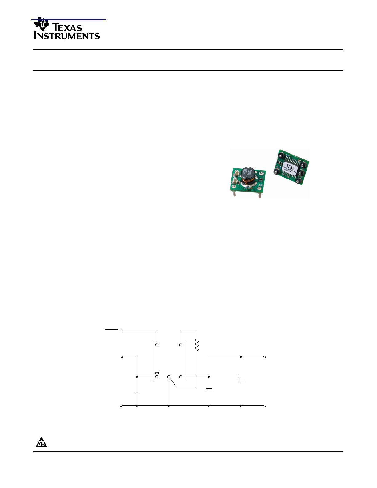
STANDARD APPLICATION
V
I
GND
GND
V
O
R
SET
(Required)
31
2
5 4
PTH04070W
(Top View)
C3*
47 F
Electroytic
(Recommended)
C2*
47 F
Ceramic
(Required)
C1*
47 F
Ceramic
(Required)
Inhibit
*See The Capacitor Application Information
#See The Specification Table for Value
0.05 W#, 1%
查询PTH04070W供应商
3-A, 3.3/5-V INPUT ADJUSTABLE SWITCHING REGULATOR
PTH04070W
SLTS227 – SEPTEMBER 2004
FEATURES
• Up to 3-A Output Current at 85 ° C
• 3.3-V / 5-V Input Voltage
• Wide-Output Voltage Adjust
• Ambient Temp. Range: –40 ° C to 85 ° C
• Surface Mount Package
• Safety Agency Approvals:
UL/CUL 60950, EN60950 VDE (Pending)
(0.9 V to 3.6 V)
• 160 W/in
3
Power Density
• Efficiencies Up To 94%
APPLICATIONS
• Telecommunications, Instumentation,
and General-Purpose Circuits
• On/Off Inhibit
• Undervoltage Lockout (UVLO)
• Output Overcurrent Protection
(Nonlatching, Auto-Reset)
• Overtemperature Protection
DESCRIPTION
The PTH04070W is a highly integrated, low-cost switching regulator module that delivers up to 3 A of output
current. Occupying less PCB area than a standard TO-220 linear regulator IC, the PTH04070W provides output
current at a much higher efficiency and with much less power dissipation, thereby eliminating the need for a heat
sink. Their small size (0.5 × 0.4 in), high efficiency, and low cost makes these modules attractive for a variety of
applications.
The input voltage range of the PTH04070W is from 3 V to 5.5 V, allowing operation from either a 3.3-V or 5-V
input bus. Using state-of-the-art switched-mode power-conversion technology, the PTH04070W can step down to
voltages as low as 0.9 V from a 5-V input bus, with typically less than 1 W of power dissipation. The output
voltage can be adjusted to any voltage over the range, 0.9 V to 3.6 V, using a single external resistor. Operating
features include an undervoltage lockout (UVLO), on/off inhibit, output overcurrent protection, and
overtemperature protection. Target applications include telecommunications, test and measurement applications,
and high-end consumer products. The modules are available in both through-hole and surface-mount package
options, including tape and reel.
PRODUCTION DATA information is current as of publication date.
Products conform to specifications per the terms of the Texas
Instruments standard warranty. Production processing does not
necessarily include testing of all parameters.
Please be aware that an important notice concerning availability, standard warranty, and use in critical applications of Texas
Instruments semiconductor products and disclaimers thereto appears at the end of this data sheet.
Copyright © 2004, Texas Instruments Incorporated
Page 2
www.ti.com
PTH04070W
SLTS227 – SEPTEMBER 2004
These devices have limited built-in ESD protection. The leads should be shorted together or the device
placed in conductive foam during storage or handling to prevent electrostatic damage to the MOS gates.
ORDERING INFORMATION
PTH04070 (Basic Model)
Output Voltage Part Number Description Package Designator
0.9 V - 3.6 V
(1) Add a T suffix for tape and reel option on SMD packages.
ABSOLUTE MAXIMUM RATINGS
over operating free-air temperature range unless otherwise noted
T
A
T
stg
(1) Stresses beyond those listed under absolute maximum ratings may cause permanent damage to the device. These are stress ratings
only, and functional operation of the device at these or any other conditions beyond those indicated under recommended operating
conditions is not implied. Exposure to absolute-maximum-rated conditions for extended periods may affect device reliability.
Operating free-air temperature Over Vinrange -40 to 85 ° C
Solder reflow temperature Surface temperature of module body or pins 235 ° C
Storage temperature -40 to 125 ° C
PTH04070WAH Horizontal T/H EVD
PTH04070WAS
(1)
Horizontal SMD EVE
(1)
PTH04070 UNIT
RECOMMENDED OPERATING CONDITIONS
V
I
T
A
Input voltage 3 5.5 V
Operating free-air temperature –40 85 ° C
PACKAGE SPECIFICATIONS
PTH04070x (Suffix AH & AS)
Weight 1.5 grams
Flammability Meets UL 94 V-O
Mechanical shock 500 Gs
Mechanical vibration Mil-STD-883D, Method 2007.2, 20-2000 Hz 20 Gs
(1) Qualification limit.
Per Mil-STD-883D, Method 2002.3, 1 msec, 1/2 sine,
mounted
MIN MAX UNIT
(1)
(1)
2
Page 3
www.ti.com
PTH04070W
SLTS227 – SEPTEMBER 2004
ELECTRICAL CHARACTERISTICS
at 25 ° C free-air temperature, VI= 5 V, VO= 3.3 V, IO= IO(Max), C1 = 47 µF, C2 = 47 µF (unless otherwise noted)
PARAMETER TEST CONDITIONS MIN TYP MAX UNIT
I
O
V
I
V
O(tol)
V
O(adj)
η Efficiency
I
O(trip)
UVLO Undervoltage lockout V
I
I(stby)
F
S
MTBF Calculated reliability 48 10
Output current TA= 85 ° C, natural convection airflow 0 3 A
Input voltage range Over IOrange 3 5.5 V
Set-point voltage tolerance TA= 25 ° C ± 2%
Temperature variation -40 ≤ TA≤ +85 ° C ±0.5% V
O
(1)
Line regulation Over VIrange ± 1 mV
Load regulation Over IOrange ± 5 mV
Total output voltage variation 3%
Output voltage adjust range V
Includes set-point, line, load,
-40 ≤ TA≤ +85 ° C
VI≥ 4.5 V 0.9 3.6
VI< 4.5 V 0.9 VI– 1.1
(1)
(2)
TA= 25 °C, IO= 2 A
R
= 475 Ω, VO= 3.3 V
SET
R
= 2.32 k Ω, VO= 2.5 V V
SET
R
= 4.87 k Ω, VO= 2 V 88%
SET
R
= 6.65 k Ω, VO= 1.8 V 87%
SET
R
= 11.5 k Ω, VO= 1.5 V 85%
SET
R
= 26.1 k Ω, VO= 1.2 V 82%
SET
R
= 84.5 k Ω, VO= 1 V 80%
SET
(2)
(2)
92%
90%
Output voltage ripple 20 MHz bandwith 10 mV
Overcurrent threshold Reset, followed by autorecovery 7 A
C3 = 47 µF, 1 A/µs load step from 50% to
100% IOmax
Transient response
Recovery time 70 µs
VOover/undershoot 100 mV
VI= increasing 2.95 3
VI= decreasing 2.7 2.8
Input high voltage (VIH) VI– 0.5 Open
(3)
Inhibit control (pin 5) Input low voltage (VIL) –0.2 0.6
Input low current (IIL) –10 µA
Input standby current Pins 5 and 2 connected 1 mA
Switching frequency Over VIand IOranges 700 kHz
External input capacitance Ceramic type (C1) 47
Ceramic type (C2) 47
External output capacitance Nonceramic type (C3) 47
Equivalent series resistance (nonceramic) 4
(4)
(5)
(5)
(7)
200
(6)
560
Per Bellcore TR-332, 50% stress,
TA= 40 ° C, ground benign
PP
V
µF
µF
m Ω
6
Hrs
(1) The set-point voltage tolerance is affected by the tolerance and stability of R
tolerance of 1% with with 100 ppm/ ° C or better temperature stability.
(2) The minimum input voltage is 3 V or (V
2 V.
+ 1.1) V, whichever is greater. A 5-V input bus is recommended for output voltages higher than
O
. The stated limit is unconditionally met if R
SET
has a
SET
(3) This control pin has an internal pullup to the input voltage VI. If it is left open circuit, the module operates when input power is applied. A
small low-leakage (<100 nA) MOS field effect transistor (MOSFET) is recommended for control. See the application information for
further guidance.
(4) An external 47-µF ceramic capacitor is required across the input (VIand GND) for proper operation. Locate the capacitor close to the
module.
(5) An external 47-µF ceramic capacitor is required across the output (V
module. Adding another 47 µF of electrolytic capacitance close to the load improves the response of the regulator to load transients.
and GND) for proper operation. Locate the capacitor close to the
O
(6) This is the calculated maximum capacitance. The minimum ESR limitation often results in a lower value. See the capacitor application
information for further guidance.
(7) This is the typical ESR for all the electrolytic (nonceramic) capacitance. Use 7 m Ω as the minimum when calculating the total equivalent
series resistance (ESR) using the max-ESR values specified by the capacitor manufacturer.
3
Page 4
www.ti.com
PTH04070W
SLTS227 – SEPTEMBER 2004
PIN ASSIGNMENT
TERMINAL FUNCTIONS
TERMINAL
NAME NO.
V
I
GND 2
V
O
VOAdjust 4 I stability of the resistor should be 100 ppm/ ° C (or better). The set-point range is from 0.9 V to 3.6 V. The
Inhibit 5 I
I/O DESCRIPTION
1 I The positive input voltage power node to the module, which is referenced to common GND.
This is the common ground connection for the VIand VOpower connections. It is also the 0 VDC
reference for the Inhibit and VOAdjust control inputs.
3 O The regulated positive power output with respect to the GND node.
A 1% resistor must be connected between this pin and GND (pin 1) to set the output voltage of the
module higher than 0.9 V. If left open-circuit, the output voltage defaults to this value. The temperature
electrical specification table gives the standard resistor value for a number of common output voltages.
Refer to the application information for further guidance.
The Inhibit pin is an open-collector/drain-negative logic input that is referenced to GND. Applying a
low-level ground signal to this input disables the module's output. When the Inhibit control is active, the
input current drawn by the regulator is significantly reduced. If the Inhibit pin is left open-circuit, the
module will produce an output voltage whenever a valid input source is applied.
4
Page 5
www.ti.com
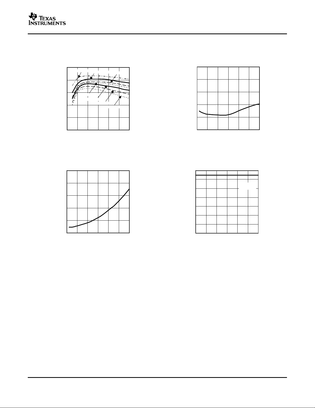
TYPICAL CHARACTERISTICS (5-V INPUT)
0 0.5 1 1.5 2 2.5 3
50
60
70
80
90
100
VO = 3.3 V
VO = 2.5 V
VO = 2 V
VO = 1.8 V
VO = 1.5 V
VO = 1.2 V
VO = 1 V
Efficiency − %
IO − Output Current − A
0
4
8
12
16
20
0 0.5 1 1.5 2 2.5 3
− Output Voltage Ripple − mV
V
O
IO − Output Current − A
PP
0
0.3
0.6
0.9
1.2
1.5
0 0.5 1 1.5 2 2.5 3
− Power Dissipation − W
P
D
IO − Output Current − A
20
30
40
50
60
70
80
90
0 0.5 1 1.5 2 2.5 3
I
O
− Output Current − A
Airflow:
Nat Conv
Temperature Derating −
C
EFFICIENCY OUTPUT RIPPLE
vs vs
OUTPUT CURRENT OUTPUT CURRENT
Figure 1. Figure 2.
PTH04070W
SLTS227 – SEPTEMBER 2004
(1) (2)
POWER DISSIPATION TEMPERATURE DERATING
vs vs
OUTPUT CURRENT OUTPUT CURRENT
Figure 3. Figure 4.
(1) The electrical characteristic data has been developed from actual products tested at 25 ° C. This data is considered typical for the
converter. Applies to Figure 1 , Figure 2 , and Figure 3 .
(2) The temperature derating curves represent the conditions at which internal components are at or below the manufacturer's maximum
operating temperatures. Derating limits apply to modules soldered directly to a 100 mm x 100 mm double-sided PCB with 1 oz. copper.
Applies to Figure 4 .
5
Page 6
www.ti.com
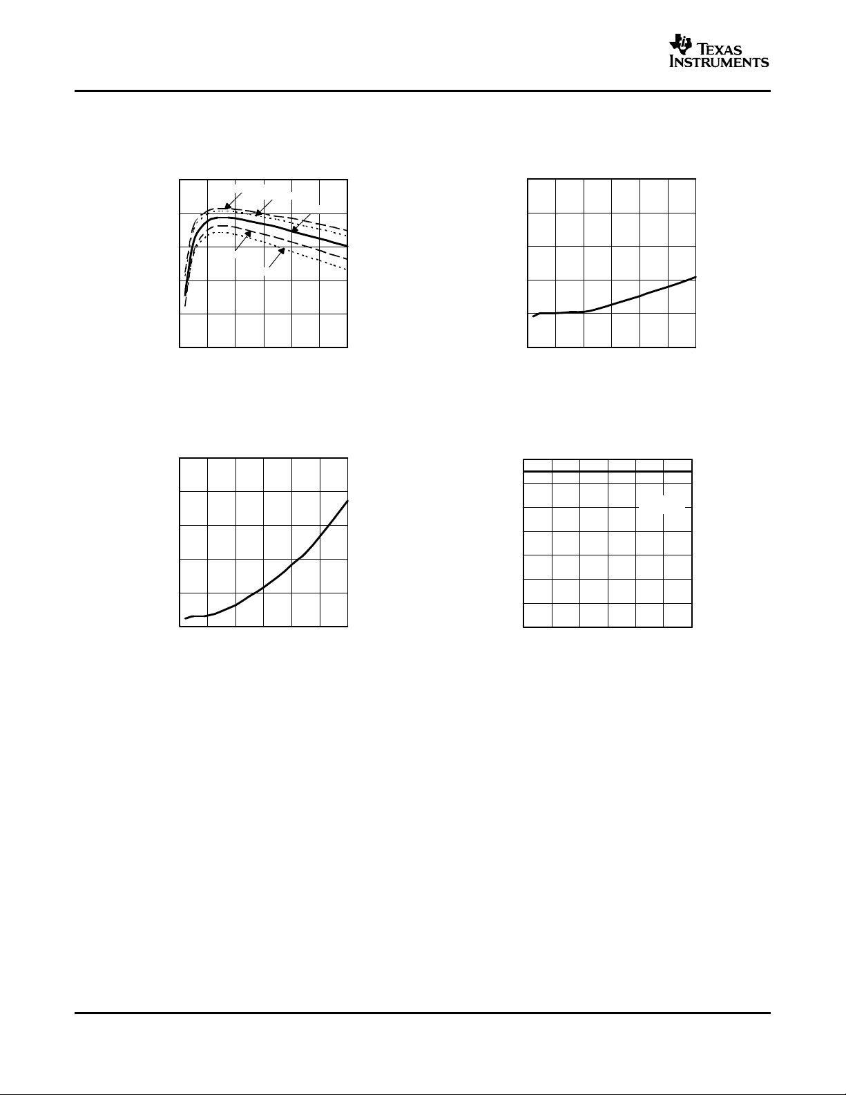
50
60
70
80
90
100
0 0.5 1 1.5 2 2.5 3
VI = 2 V
VI = 1.8 V
VI = 1.5 V
VI = 1.2 V
VI = 1 V
Efficiency − %
IO − Output Current − A
0
4
8
12
16
20
0 0.5 1 1.5 2 2.5 3
I
O
− Output Current − A
− Output Voltage Ripple − mV
V
O
PP
0
0.3
0.6
0.9
1.2
1.5
0 0.5 1 1.5 2 2.5 3
− Power Dissipation − W
P
D
IO − Output Current − A
20
30
40
50
60
70
80
90
0 0.5 1 1.5 2 2.5 3
I
O
− Output Current − A
Airflow:
Nat Conv
Temperature Derating −
C
PTH04070W
SLTS227 – SEPTEMBER 2004
TYPICAL CHARACTERISTICS (3.3-V INPUT)
EFFICIENCY OUTPUT RIPPLE
vs vs
OUTPUT CURRENT OUTPUT CURRENT
Figure 5. Figure 6.
(3) (4)
POWER DISSIPATION TEMPERATURE DERATING
vs vs
OUTPUT CURRENT OUTPUT CURRENT
Figure 7. Figure 8.
(3) The electrical characteristic data has been developed from actual products tested at 25 ° C. This data is considered typical for the
converter. Applies to Figure 5 , Figure 6 , and Figure 7 .
(4) The temperature derating curves represent the conditions at which internal components are at or below the manufacturer's maximum
operating temperatures. Derating limits apply to modules soldered directly to a 100 mm x 100 mm double-sided PCB with 1 oz. copper.
Applies to Figure 8 .
6
Page 7

www.ti.com
R
set
10 k
0.891 V
V
out
0.9 V
3.24 k
Inhibit
GND GND
R
SET
0.05 W
1%
C1
Ceramic
C2
Ceramic
PTH04070W
2
4
31
5
VO AdjGND
V
O
V
IN
47-µF 47-µF
V
I
V
O
Inhibit
SLTS227 – SEPTEMBER 2004
APPLICATION INFORMATION
Adjusting the Output Voltage of the PTH04070W Wide-Output Adjust Power Modules
The V
0.9 V to 3.6 V. The adjustment method requires the addition of a single external resistor, R
connected directly between the V
number of common bus voltages, along with the actual voltage the resistance produces.
For other output voltages, the value of the required resistor can either be calculated using the following formula,
or simply selected from the range of values given in Table 2 . Figure 9 shows the placement of the required
resistor.
Adjust control (pin 4) sets the output voltage of the PTH04070W product. The adjustment range is from
O
Adjust and GND pin 2. Table 1 gives the standard external resistor for a
O
PTH04070W
, that must be
set
Table 1. Standard Values of R
Voltages
V
out
(Required) (Standard Value) (Actual)
(1)
3.3 V
(1)
2.5 V
2 V 4.87 k Ω 1.999 V
1.8 V 6.65 k Ω 1.801 V
1.5 V 11.5 k Ω 1.504 V
1.2 V 26.1 k Ω 1.204 V
1 V 84.5 k Ω 1.001 V
0.9 V Open 0.9 V
(1) The minimum input voltage is 3 V or (V
greater.
R
set
475 Ω 3.298 V
2.32 k Ω 2.502 V
for Common Output
set
+ 1.1) V, whichever is
O
V
out
(1) A 0.05-W rated resistor may be used. The tolerance should be 1%, with a temperature stability of 100 ppm/ ° C (or
better). Place the resistor as close to the regulator as possible. Connect the resistor directly between pins 4 and 2
using dedicated PCB traces.
(2) Never connect capacitors from VOAdjust to either GND or VO. Any capacitance added to the VOAdjust pin will affect
the stability of the regulator.
Figure 9. V
O
Adjust Resistor Placement
7
Page 8

www.ti.com
PTH04070W
SLTS227 – SEPTEMBER 2004
Table 2. Calculated Set-Point Resistor Values
VaReq'd R
0.900 Open 1.475 12.3 k Ω 2.55 2.16 k Ω
0.925 353 k Ω 1.50 11.6 k Ω 2.60 2.00 k Ω
0.950 175 k Ω 1.55 10.5 k Ω 2.65 1.85 k Ω
0.975 116 k Ω 1.60 9.49 k Ω 2.70 1.71 k Ω
1.000 85.9 k Ω 1.65 8.64 k Ω 2.75 1.58 k Ω
1.025 68.0 k Ω 1.70 7.90 k Ω 2.80 1.45 k Ω
1.050 56.2 k Ω 1.75 7.24 k Ω 2.85 1.33 k Ω
1.075 47.7 k Ω 1.80 6.66 k Ω 2.90 1.22 k Ω
1.100 41.3 k Ω 1.85 6.14 k Ω 2.95 1.11 k Ω
1.125 36.4 k Ω 1.90 5.67 k Ω 3.00 1.00 k Ω
1.150 32.4 k Ω 1.95 5.25 k Ω 3.05 904 Ω
1.175 29.2 k Ω 2.00 4.86 k Ω 3.10 810 Ω
1.200 26.5 k Ω 2.05 4.51 k Ω 3.15 720 Ω
1.225 24.2 k Ω 2.10 4.19 k Ω 3.20 634 Ω
1.250 22.2 k Ω 2.15 3.89 k Ω 3.25 551 Ω
1.275 20.5 k Ω 2.20 3.61 k Ω 3.30 473 Ω
1.300 19.0 k Ω 2.25 3.36 k Ω 3.35 397 Ω
1.325 17.7 k Ω 2.30 3.12 k Ω 3.40 324 Ω
1.350 16.6 k Ω 2.35 2.90 k Ω 3.45 254 Ω
1.375 15.5 k Ω 2.40 2.70 k Ω 3.50 187 Ω
1.400 14.6 k Ω 2.45 2.51 k Ω 3.55 122 Ω
1.425 13.7 k Ω 2.50 2.33 k Ω 3.60 60 Ω
1.450 13.0 k Ω
set
VaReq'd R
set
VaReq'd R
set
8
Page 9

www.ti.com
PTH04070W
SLTS227 – SEPTEMBER 2004
CAPACITOR RECOMMENDATIONS for the PTH04070W WIDE-OUTPUT
ADJUST POWER MODULES
Input Capacitor
The minimum recommended input capacitor(s) is 47-µF of ceramic capacitance, in either an X5R or X7R
temperature tolerance. The ceramic capacitors should be located within 0.5 in. (1,27 cm) of the regulator's input
pins. Electrolytic capacitors can also be used at the input, but only in addition to the required ceramic
capacitance. The minimum ripple current rating for nonceramic capacitors should be at least 200 mA rms. The
ripple current rating of electrolytic capacitors is a major consideration when they are used at the input.
When specifying regular tantalum capacitors for use at the input, a minimum voltage rating of 2 × (maximum dc
voltage + ac ripple) is highly recommended. This is standard practice to ensure reliability. Polymer-tantalum
capacitors are not affected by this requirement.
For improved ripple reduction on the input bus, additional ceramic capacitors can be used to complement the
minimum requirement.
Output Capacitors
For most applications only one (1) 47-µF ceramic capacitor is required. The ceramic capacitor should be located
within 0.5 in. (1,27 cm) of the output pin. Adding a second 47-µF nonceramic capacitor allows the module to
meet its transient response specification. For applications with load transients (sudden changes in load current),
the regulator response benefits from additional external output capacitance. A high-quality computer-grade
electrolytic capacitor should be adequate.
Electrolytic capacitors should be located close to the load circuit. These capacitors provide decoupling over the
frequency range, 2 kHz to 150 kHz. Aluminum electrolytic capacitors are suitable for ambient temperatures
above 0 ° C. For operation below 0 ° C, tantalum or Os-Con type capacitors are recommended. When using one or
more nonceramic capacitors, the calculated equivalent ESR should be no lower than 4 mΩ (7 m Ω using the
manufacturer's maximum ESR for a single capacitor). A list of preferred low-ESR type capacitors are identified in
Table 3 , the recommended capacitor table.
Ceramic Capacitors
Above 150 kHz the performance of aluminum electrolytic capacitors becomes less effective. To further improve
the reflected input ripple current, or the output transient response, multilayer ceramic capacitors must be added.
Ceramic capacitors have very low ESR and their resonant frequency is higher than the bandwidth of the
regulator. When placed at the output their combined ESR is not critical as long as the total value of ceramic
capacitance does not exceed 200 µF. Also, to prevent the formation of local resonances, do not place more than
three identical ceramic capacitors with values of 10 µF or greater in parallel.
Tantalum Capacitors
Additional tantalum type capacitors can be used at both the input and output, and are recommended for
applications where the ambient operating temperature can be less than 0 ° C. The AVX TPS, Sprague
593D/594/595 and Kemet T495/T510/T520 capacitors series are suggested over many other tantalum types due
to their rated surge, power dissipation, and ripple current capability. As a caution, many general-purpose
tantalum capacitors have considerably higher ESR, reduced power dissipation, and lower ripple current
capability. These capacitors are also less reliable as they have lower power dissipation and surge current ratings.
Tantalum capacitors that do not have a stated ESR or surge current rating are not recommended for power
applications. When specifying Os-Con and polymer tantalum capacitors for the output, the minimum ESR limit is
encountered well before the maximum capacitance value is reached.
Capacitor Table
The capacitor table, Table 3 , identifies the characteristics of capacitors from a number of vendors with
acceptable ESR and ripple current (rms) ratings. The recommended number of capacitors required at both the
input and output buses is identified for each capacitor type. This is not an extensive capacitor list. Capacitors
from other vendors are available with comparable specifications. Those listed are for guidance. The rms rating
and ESR (at 100 kHz) are critical parameters necessary to insure both optimum regulator performance and long
capacitor life.
9
Page 10

www.ti.com
PTH04070W
SLTS227 – SEPTEMBER 2004
Designing for Load Transients
The transient response of the dc/dc converter has been characterized using a load transient with a di/dt of 1
A/µs. The typical voltage deviation for this load transient is given in the data sheet specification table using the
optional value of output capacitance. As the di/dt of a transient is increased, the response of a converter's
regulation circuit ultimately depends on its output capacitor decoupling network. This is an inherent limitation with
any dc/dc converter once the speed of the transient exceeds its bandwidth capability. If the target application
specifies a higher di/dt or lower voltage deviation, the requirement can only be met with additional output
capacitor decoupling. In these cases, special attention must be paid to the type, value, and ESR of the
capacitors selected.
If the transient performance requirements exceed those specified in the data sheet, the selection of output
capacitors becomes more important. Review the minimum ESR in the characteristic data sheet for details on the
capacitance maximum.
Table 3. Recommended Input/Output Capacitors
CAPACITOR CHARACTERISTICS QUANTITY
CAPACITOR VENDOR/
COMPONENT
SERIES
Panasonic WA (SMT) 10 V 120 0.035 Ω 2800 mA 8 × 6.9 1 ≤ 4
FC (SMT) 25 V 47 0.400 Ω 230 mA 8 × 6.2 1 1
Panasonic SL SP-cap(SMT) 6.3 V 47 0.018 Ω 2500 mA 7.3 × 4.3 1 ≤ 3 EEFCD0J470R
United Chemi-con PXA (SMT) 10 V 47 0.031 Ω 2250 mA 6.3 × 5.7 1 1 PXA10VC470MF60TP
FS 10 V 100 0.040 Ω 2100 mA 6.3 × 9.8 1 ≤ 5 10FS100M
LXZ 16 V 100 0.250 Ω 290 mA 6.3 × 11.5 1 1 LXZ16VB101M6X11LL
MVZ (SMT) 16 V 100 0.440 Ω 230mA 6.3 × 5.7 1 1 MVZ16VC101MF60TP
Nichicon UWG (SMT) 16 V 100 0.400 Ω 230mA 8 × 6.2 1 1 UWG1C101MCR1GS
F559(Tantalum) 10 V 100 0.055 Ω 2000mA 7.7 × 4.3 1 ≤ 5 F551A107MN
PM 10 V 100 0.550 Ω 210 mA 6 × 11 1 1 UPM1A101MEH
Sanyo Os-con\ POS-Cap SVP 10V 68 0.025 Ω 2400 mA 7.3 × 4.3 1 ≤ 5 10TPE68M
(SMT) 6.3 V 47 0.074 Ω 1110 mA 5 × 6 1 ≤ 5 6SVP47M
SP 10 V 56 0.045 Ω 1710 mA 6.3 × 5.0 1 ≤ 5 10SP56M
AVX Tantalum TPS (SMD) 10 V 47 0.100 Ω 1100 mA 7.3L × 4.3W 1 ≤ 5 TPSD476M010R0100
Kemet T520 (SMD) 10 V 68 0.060 Ω >1200 mA 7.3L × 5.7W 1 ≤ 5 T520V686M010ASE060
AO-CAP 6.3 V 47 0.028 Ω >1100 mA × 4.0H 1 ≤ 3 A700V476M006AT
Vishay/Sprague 594D/595D 10 V 68 0.100 Ω >1000 mA 7.3L × 6.0W 1 ≤ 5 594D686X0010C2T
(SMD) 10 V 68 0.240 Ω 680 mA × 4.1H 1 ≤ 5 595D686X0010C2T
94SL 16 V 47 0.070 Ω 1550 mA 8 × 5 1 ≤ 5 94SL476X0016EBP
TDK Ceramic X5R 6.3 V 22 0.002 Ω >1400 mA 1210 case ≥ 2
Murata Ceramic X5R 6.3 V 22 0.002 Ω >1000 mA 3225 mm ≥ 2
Kemet 6.3 V 22 0.002 Ω >1000 mA ≥ 2
TDK Ceramic X5R 6.3 V 47 0.002 Ω >1400 mA 1210 case ≥ 1 ≤ 3 C3225X5R0J476KT/MT
Murata Ceramic X5R 6.3 V 47 0.002 Ω >1000 mA 3225 mm ≥ 1 ≤ 3 GRM32ER60J476M/6.3
Kemet 6.3 V 47 0.002 Ω >1000 mA ≥ 1 ≤ 3 C1210C476K9PAC
WORKING VALUE SERIES INPUT OUTPUT
VOLTAGE µF RESISTANCE BUS
6.3 V 56 0.009 Ω 3000 mA 7.3 × 4.3 1 ≤ 2 EEFSL0J560R
10 V 47 0.060 Ω > 412 mA × 4.1H 1 ≤ 5 TPSB476M010R0500
EQUIVALENT
(ESR)
(1) A ceramic capacitor is required on both the input and the output. An electrolytic capacitor can be added to the output for improved
transient response.
(2) An optional through-hole capacitor available.
(3) A total capacitance of 44 µF is an acceptable replacement for a single 47-µF capacitor.
85 ° C
MAXIMUM PHYSICAL
RIPPLE SIZE
CURRENT (mm)
(I
)
rms
VENDOR
(1)
BUS
(1)
(1)
(3)
≤ 3 C3225X5R0J226KT/MT
(3)
≤ 3 GRM32ER61J223M
(3)
≤ 3 C1210C226K9PAC
NUMBER
EEFWA1A121P
EEVFC1E470P
(2)
(2)
10
Page 11

www.ti.com
t − 10 ms/div
VI (1 V/div)
V
O
(1 V/div)
I
I
(1 A/div)
PTH04070W
SLTS227 – SEPTEMBER 2004
Power-Up Characteristics
When configured per the standard application, the PTH04070 power module produces a regulated output voltage
following the application of a valid input source voltage. During power up, internal soft-start circuitry slows the
rate that the output voltage rises, thereby limiting the amount of in-rush current that can be drawn from the input
source. The soft-start circuitry introduces a short time delay (typically 10 ms) into the power-up characteristic.
This is from the point that a valid input source is recognized. Figure 10 shows the power-up waveforms for a
PTH04070W, operating from a 3-V input and with the output voltage adjusted to 1.8 V. The waveforms were
measured with a 2-A resistive load.
Figure 10. Power-Up Waveforms
Current Limit Protection
The PTH04070 modules protect against load faults with a continuous current limit characteristic. Under a load
fault condition, the output current cannot exceed the current limit value. Attempting to draw current that exceeds
the current limit value causes the output voltage to be progressively reduced. Current is continuously supplied to
the fault until it is removed. Upon removal of the fault, the output voltage will promptly recover.
Thermal Shutdown
Thermal shutdown protects the module internal circuitry against excessively high temperatures. A rise in
temperature may be the result of a drop in airflow, a high ambient temperature, or a sustained current limit
condition. If the junction temperature of the internal components exceeds 150 ° C, the module shuts down. This
reduces the output voltage to zero. The module will start up automatically, by initiating a soft-start power up when
the sensed temperature decreases 10 ° C below the thermal shutdown trip point.
Output On/Off Inhibit
For applications requiring output voltage on/off control, the PTH04070 power module incorporates an output
on/off Inhibit control (pin 5). The inhibit feature can be used wherever there is a requirement for the output
voltage from the regulator to be turned off.
The power module functions normally when the Inhibit pin is left open-circuit, providing a regulated output
whenever a valid source voltage is connected to Vin with respect to GND.
Figure 11 shows the typical application of the inhibit function. Note the discrete transistor (Q1). The Inhibit control
has its own internal pullup to VIpotential. An open-collector or open-drain device is recommended to control this
input.
11
Page 12

www.ti.com
Inhibit
GND
GND
R
SET
0.05 W
1%
C1
Ceramic
C2
Ceramic
PTH04070W
2
4
31
5
VO AdjGND
V
O
V
IN
47-µF
47-µF
V
I
= 5 V VO = 1.8 V
Inhibit
BSS138
Q1
6.65 k
L
O
A
D
t − 5 ms/div
VO (1 V/div)
I
I
(1 A/div)
Q1, Vgs (10 V/div)
PTH04070W
SLTS227 – SEPTEMBER 2004
Turning Q1 on applies a low voltage to the Inhibit control pin and disables the output of the module. If Q1 is then
turned off, the module will execute a soft-start power-up sequence. A regulated output voltage is produced within
20 msec. Figure 12 shows the typical rise in the output voltage, following the turn off of Q1. The turn off of Q1
corresponds to the fall in the waveform, Q1 Vgs. The waveforms were measured with a 2-A resistive load.
Figure 11. On/Off Inhibit Control Circuit
Figure 12. Power Up Response From Inhibit Control
12
Page 13

Page 14

Page 15

IMPORTANT NOTICE
Texas Instruments Incorporated and its subsidiaries (TI) reserve the right to make corrections, modifications,
enhancements, improvements, and other changes to its products and services at any time and to discontinue
any product or service without notice. Customers should obtain the latest relevant information before placing
orders and should verify that such information is current and complete. All products are sold subject to TI’s terms
and conditions of sale supplied at the time of order acknowledgment.
TI warrants performance of its hardware products to the specifications applicable at the time of sale in
accordance with TI’s standard warranty. Testing and other quality control techniques are used to the extent TI
deems necessary to support this warranty . Except where mandated by government requirements, testing of all
parameters of each product is not necessarily performed.
TI assumes no liability for applications assistance or customer product design. Customers are responsible for
their products and applications using TI components. To minimize the risks associated with customer products
and applications, customers should provide adequate design and operating safeguards.
TI does not warrant or represent that any license, either express or implied, is granted under any TI patent right,
copyright, mask work right, or other TI intellectual property right relating to any combination, machine, or process
in which TI products or services are used. Information published by TI regarding third-party products or services
does not constitute a license from TI to use such products or services or a warranty or endorsement thereof.
Use of such information may require a license from a third party under the patents or other intellectual property
of the third party, or a license from TI under the patents or other intellectual property of TI.
Reproduction of information in TI data books or data sheets is permissible only if reproduction is without
alteration and is accompanied by all associated warranties, conditions, limitations, and notices. Reproduction
of this information with alteration is an unfair and deceptive business practice. TI is not responsible or liable for
such altered documentation.
Resale of TI products or services with statements different from or beyond the parameters stated by TI for that
product or service voids all express and any implied warranties for the associated TI product or service and
is an unfair and deceptive business practice. TI is not responsible or liable for any such statements.
Following are URLs where you can obtain information on other Texas Instruments products and application
solutions:
Products Applications
Amplifiers amplifier.ti.com Audio www.ti.com/audio
Data Converters dataconverter.ti.com Automotive www.ti.com/automotive
DSP dsp.ti.com Broadband www.ti.com/broadband
Interface interface.ti.com Digital Control www.ti.com/digitalcontrol
Logic logic.ti.com Military www.ti.com/military
Power Mgmt power.ti.com Optical Networking www.ti.com/opticalnetwork
Microcontrollers microcontroller.ti.com Security www.ti.com/security
Telephony www.ti.com/telephony
Video & Imaging www.ti.com/video
Wireless www.ti.com/wireless
Mailing Address: Texas Instruments
Post Office Box 655303 Dallas, Texas 75265
Copyright 2004, Texas Instruments Incorporated
Page 16

Copyright © Each Manufacturing Company.
All Datasheets cannot be modified without permission.
This datasheet has been download from :
www.AllDataSheet.com
100% Free DataSheet Search Site.
Free Download.
No Register.
Fast Search System.
www.AllDataSheet.com
 Loading...