

For assistance or to order, call (800) 531-5782
PT79SR100 Series
-1.5 AMP NEGATIVE STEP-DOWN
INTEGRATED SWITCHING REGULATOR
Application Notes
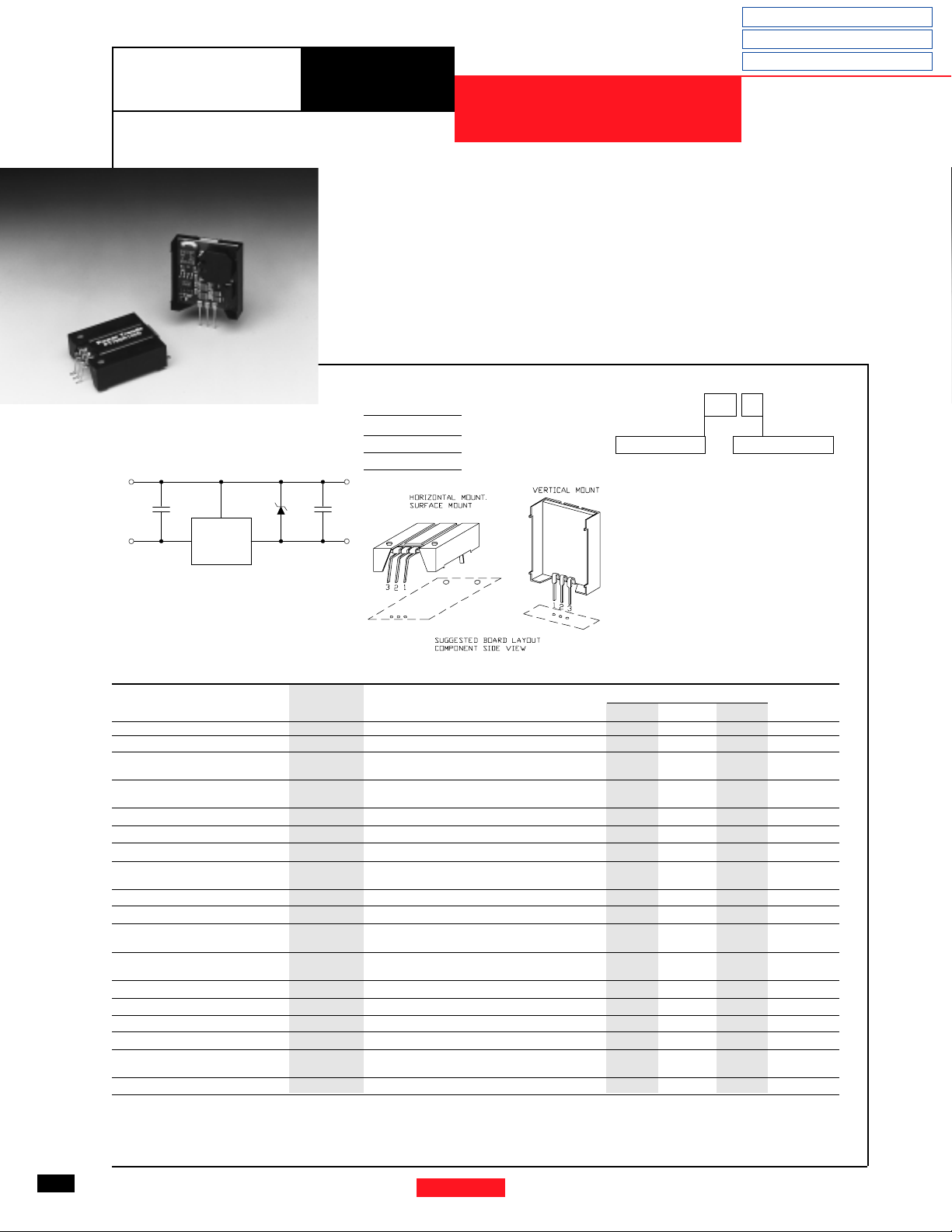
Mechanical Outline
Product Selector Guide
Revised 5/15/98
Standard Application
C1
-Vin
C1 = Optional ceramic (1µF)
C2 = Optional ceramic (1-5µF)
D1 = Zener diode required to clamp
1
23
PT79SR1
turn-on overshoot
(See Application Note)
• High Efficiency > 85%
• Self-Contained Inductor
• Short Circuit Protection
• Over-Temperature Protection
Regulators (ISRs). These ISRs have a
maximum output current of -1.5 Amps
and an output voltage that is laser
trimmed to most industry standard voltages. They have excellent line and load
The PT79SR100 Series is a new
line of Negative Input/Negative Output 3-terminal Integrated Switching
Pin-Out Information
Pin Function
1 GND
2-V
in
3-V
COMCOM
C2D1
-Vout
out
regulation, and are ideal for applications,
such as RS232 and Ethernet communications, ECL logic, and op-amp circuitry.
Ordering Information
PT79SR1
Output Voltage
05 = -5.0 Volts
52 = -5.2 Volts
08 = -8.0 Volts
09 = -9.0 Volts
12 = -12.0 Volts
15 = -15.0 Volts
Y
XX
Package Suffix
V = Vertical Mount
S = Surface Mount
H = Horizontal
Mount
Specifications
Pkg Style 500
Characteristics
(Ta = 25°C unless noted) Symbols Conditions Min Typ Max Units
Output Current I
Short Circuit Current I
Input Voltage Range V
Output Voltage Tolerance ∆V
Line Regulation Reg
Load Regulation Reg
V
Ripple/Noise V
o
Transient Response t
Efficiency η Vin=-10V, Io=-1.0A, Vo=-5V — 85 — %
Switching Frequency ƒ
Absolute Maximum T
Operating Temperature Range
Recommended Operating T
Temperature Range Over Vin and Io ranges
Thermal Resistance θ
Temperature Coefficient T
Storage Temperature T
Mechanical Shock — Per Mil-STD-883D, Method 2002.3 — 500 — G’s
Mechanical Vibration — Per Mil-STD-883D, Method 2007.2,
Weight — — — 7.0 — Grams
* ISR will operate down to no load with reduced specifications. ** See Thermal Derating chart.
o
sc
in
o
line
load
n
tr
o
a
a
ja
c
s
Over Vin range -0.1* — -1.5 A
Vin=Vo-4V — -3.5 — Apk
Io=-0.1 to -1.5 A Vo=-5V -9 — -30 V
-0.1 ≥ Io ≥ -1.5 A Vo=-15V -19 — -30 V
Over Vin range, Io=-1.5 A
Ta=-20°C to shutdown
Over Vin range — ±1.0 ±2.0 %V
-0.1 ≤ Io ≤ -1.5 A — ±0.5 ±1.0 %V
Vin=-15V, Io=-1.0 A,Vo=-5V — 35 — mV
50% load change — 100 — µSec
Vo=overshoot/undershoot — 30 — %V
Over Vin and Io ranges 0.95 1.0 1.05 MHz
Free Air Convection, (40-60LFM)
Free Air Convection, (40-60LFM) — 45 — °C/W
Over Vin and Io ranges — ±0.5 ±1.5 mV/°C
— -40 — +125 °C
20-2000 Hz, soldered in a PC board
PT79SR100 SERIES
— ±1.0 ±3.0 %V
-40 — +85 °C
-40 — +60** °C
—5
—
o
o
o
pp
o
G’s
22
Power Trends, Inc. 27715 Diehl Road, Warrenville, IL 60555 (800) 531-5782 Fax: (630) 393-6902 http://www.powertrends.com
For assistance or to order, call (800) 531-5782
PT79SR100 Series
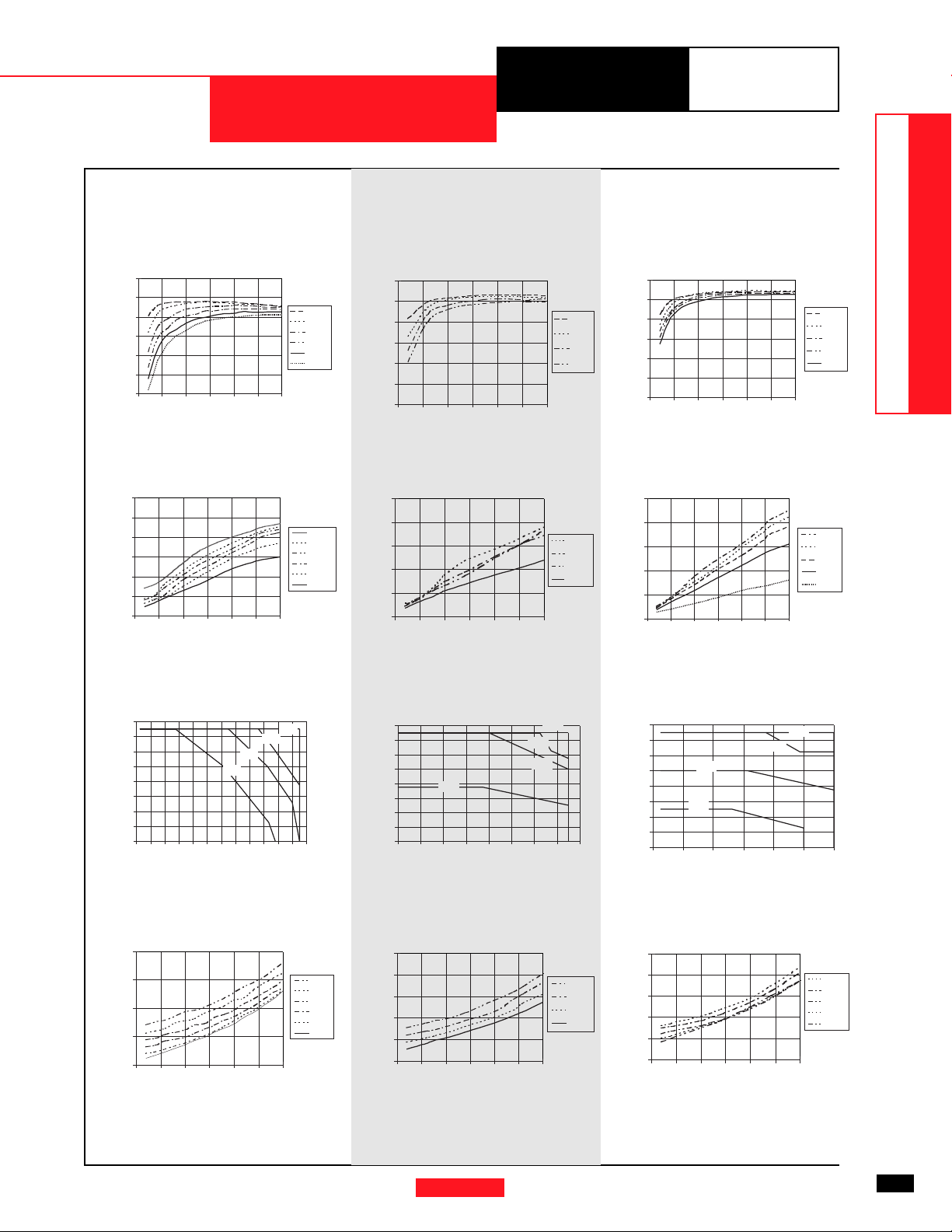
CHARACTERISTIC DATA
PT79SR105, -5.0 VDC (See Note 1)
PT79SR112, -12.0 VDC (See Note 1)
Efficiency vs Output Current Efficiency vs Output Current Efficiency vs Output Current
100
90
80
70
Efficiency - %Ripple-(mV)Iout-(Amps)PD-(Watts)
60
50
40
0 0.25 0.5 0.75 1 1.25 1.5
Iout-(Amps)
Vin
9V
10.0V
15.0V
20.0V
25.0V
30.0V
100
90
80
70
Efficiency - %Ripple-(mV)Iout-(Amps)PD-(Watts)
60
50
40
0 0.25 0.5 0.75 1 1.25 1.5
Iout-(Amps)
Vin
16.0V
20.0V
25.0V
30.0V
Ripple vs Output Current Ripple vs Output Current Ripple vs Output Current
60
50
40
30
20
10
0
0 0.25 0.5 0.75 1 1.25 1.5
Iout-(Amps)
Vin
30.0V
25.0V
20.0V
15.0V
10.0V
9V
100
80
60
40
20
0
0 0.25 0.5 0.75 1 1.25 1.5
Iout-(Amps)
Vin
30.0V
25.0V
20.0V
16.0V
PT79SR115, -15.0 VDC (See Note 1)
100
90
80
70
Efficiency - %Ripple-(mV)Iout-(Amps)PD-(Watts)
60
50
40
0 0.25 0.5 0.75 1 1.25 1.5
Iout-(Amps)
150
120
90
60
30
0
0 0.25 0.5 0.75 1 1.25 1.5
Iout-(Amps)
Vin
Vin
30.0V
27.0V
24.0V
21.0V
19.0V
19.0V
21.0V
24.0V
27.0V
30.0V
Wide Input Range Products
DATA SHEETS
Thermal Derating (Ta) (See Note 2) Thermal Derating (Ta) (See Note 2) Thermal Derating (Ta) (See Note 2)
1.6
1.4
1.2
1
0.8
0.6
0.4
0.2
0
7 9 11 13 15 17 19 21 23 25 27 29 31
70˚C
85˚C
Vin-(Volts)
60˚C
50˚C
1.6
1.4
1.2
1
0.8
0.6
0.4
0.2
0
15 17 19 21 23 25 27 29 31
85˚C
Vin-(Volts)
60˚C
70˚C
50˚C
1.6
1.4
1.2
1
0.8
0.6
0.4
0.2
0
18 20 22 24 26 28 30
70˚C
85˚C
Vin-(Volts)
Power Dissipation vs Output Current Power Dissipation vs Output Current Power Dissipation vs Output Current
2
1.5
1
0.5
0
0 0.25 0.5 0.75 1 1.25 1.5
Vin
30.0V
25.0V
20.0V
15.0V
10.0V
9V
Iout-(Amps)
Note 1: All data listed in the above graphs, except for derating data, has been developed from actual products tested at 25°C. This data is considered typical data for the ISR.
Note 2: Thermal derating graphs are developed in free air convection cooling of 40-60 LFM soldered in a printed circuit board. (See Thermal Application Notes.)
2.5
2
1.5
1
0.5
0
0 0.25 0.5 0.75 1 1.25 1.5
Iout-(Amps)
Vin
30.0V
25.0V
20.0V
16.0V
2.5
2
1.5
1
0.5
0
0 0.25 0.5 0.75 1 1.25 1.5
Iout-(Amps)
60˚C
50˚C
Vin
30.0V
27.0V
24.0V
21.0V
19.0V
Power Trends, Inc. 27715 Diehl Road, Warrenville, IL 60555 (800) 531-5782 Fax: (630) 393-6902 http://www.powertrends.com
23
 Loading...