

Page 1
查询PT78ST100供应商
PT78ST100 Series
1.5 Amp Positive Step-Down
Integrated Switching Regulator
SLTS059A
(Revised 6/30/2000)
• Very Small Footprint
• High Efficiency > 85%
• Self-Contained Inductor
• Internal Short-Circuit Protection
• Over-Temperature Protection
• Fast Transient Response
• Wide Input Range
These ISRs have a maximum output current
of 1.5 Amps and an output voltage that is laser
trimmed to a variety of industry standard voltages.
These 78 series regulators have excellent line and load regulation with internal
short- circuit and over-temperature protection, and are offered in a variety of standard
The PT78ST100 is a series of wide-
input range, 3-terminal regulators.
output voltages. These ISRs are very flexible and may be used in a wide variety of
applications.
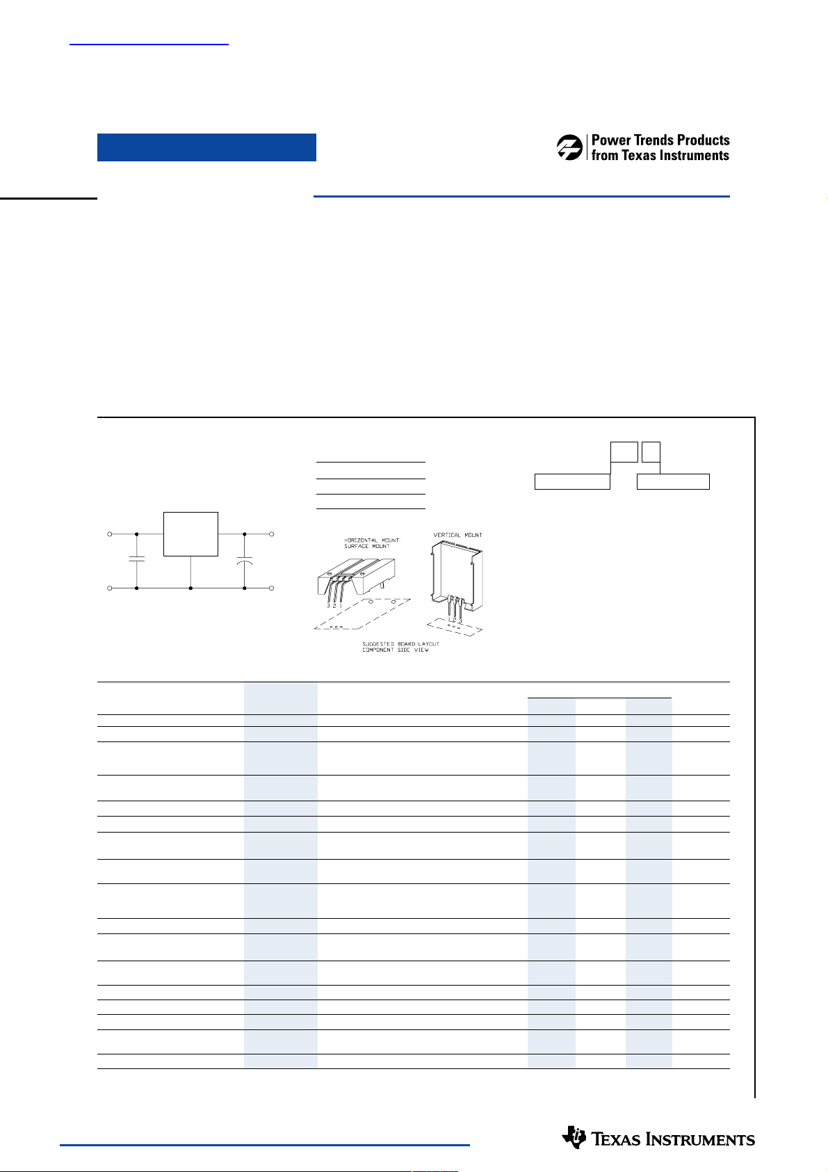
Pin-Out Information
Pin Function
1V
in
Standard Application
C2
Vout
+
COMCOM
Vin
C1
1
C1 = Optional 1µF ceramic
C2
= Required 100µF electrolytic
PT78ST100
2
3
Specifications
Characteristics
(Ta = 25°C unless noted) Symbols Conditions Min Typ Max Units
Output Current I
Short Circuit Current I
Input Voltage Range V
Output Voltage Tolerance ∆V
Line Regulation Reg
Load Regulation Reg
Ripple/Noise V
V
o
Transient Response t
(with 100µF output cap) Vo over/undershoot — 5 — %V
Efficiency η V
Switching Frequency ƒ
Absolute Maximum T
Operating Temperature Range
Recommended Operating T
Temperature Range At Vin= 24V, Io=1.0A
Thermal Resistance θ
Storage Temperature T
Mechanical Shock — Per Mil-STD-883D, Method 2002.3 — 500 — G’s
Mechanical Vibration — Per Mil-STD-883D, Method 2007.2,
Weight — — — 6.5 — grams
*ISR will operate down to no load with reduced specifications. **See Thermal Derating chart.
Note:
The PT78ST100 Series requires a 100µF electrolytic or tantalum output capacitor for proper operation in all applications.
o
sc
in
o
line
load
n
tr
o
a
a
ja
s
2 GND
3V
out
Pkg Style 500
Over Vin range 0.1* — 1.5 A
Vin = V
min — 3.5 — Apk
in
0.1 ≤ Io ≤ 1.5A V
Over Vin range, Io=1.5A
Ta = 0°C to +60°C
Over Vin range — ±0.2 ±0.4 %V
0.1 ≤ Io ≤ 1.5A — ±0.1 ±0.2 %V
Vin= 9V, Io= 1.5A Vo= 5V — 65 — mV
Vin= 16V, Io= 1.5A Vo= 12V 90 mV
50% load change — 100 — µSec
= 10V, Io= 1A Vo= 3.3V — 80 — %
in
= 10V, Io= 1A Vo= 5V — 85 — %
V
in
Vin= 17V, Io= 1A Vo= 12V — 90 — %
Over Vin range, Io=1.5A 600 650 700 kHz
—
Free Air Convection, (40-60LFM)
Free Air Convection, (40-60LFM) — 45 — °C/W
— -40 — +125 °C
20-2000 Hz, soldered in a PC board
= 3.3V 9 — 26 V
o
V
= 5V 9 — 38 V
o
Vo= 12V 16 — 38 V
Ordering Information
PT78ST1
Output Voltage
33 = 3.3 Volts
36 = 3.6 Volts
05 = 5.0 Volts
51 = 5.1 Volts
53 = 5.25 Volts
06 = 6.0 Volts
65 = 6.5 Volts
07 = 7.0 Volts
08 = 8.0 Volts
09 = 9.0 Volts
10 = 10.0 Volts
12 = 12.0 Volts
14 = 13.9 Volts
15 = 15.0 Volts
PT78ST100 SERIES
— ±1.0 ±2.0 %V
-40 — +85 °C
-40 — +80** °C
—5
XX Y
Package Suffix
V = Vertical Mount
S = Surface Mount
H = Horizontal
Mount
—
G’s
o
o
o
pp
pp
o
For technical support and more information, see inside back cover or visit www.ti.com/powertrends
Page 2
PT78ST100 Series
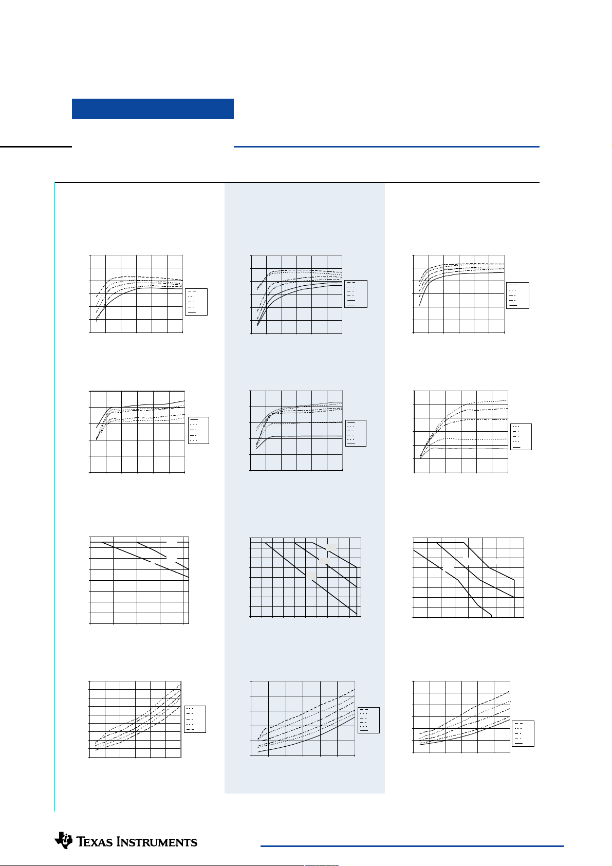
Typical Characteristics
1.5 Amp Positive Step-Down
Integrated Switching Regulator
PT78ST133, 3.3 VDC (See Note 1) PT78ST105, 5.0 VDC (See Note 1) PT78ST112, 12.0 VDC (See Note 1)
Efficiency vs Output Current Efficiency vs Output Current
100
90
80
70
60
Efficiency - %Ripple-(mV)Iout-(Amps)PD-(Watts)
50
40
0 0.25 0.5 0.75 1 1.25 1.5
Iout-(Amps)
Vin
9.0V
12.0V
15.0V
20.0V
26.0V
100
90
80
70
Efficiency - %
60
50
40
0 0.25 0.5 0.75 1 1.25 1.5
Iout-(Amps)
Ripple vs Output Current Ripple vs Output Current
100
80
60
40
20
0
00.250.50.7511.251.5
Iout-(Amps)
Thermal Derating (T
1.6
1.4
1.2
1
0.8
0.6
0.4
0.2
0
913172125
) (See Note 2) Thermal Derating (Ta) (See Note 2)
a
60°C
70°C
85°C
Vin-(Volts) Vin-(Volts)Vin-(Volts)
Vin
26.0V
20.0V
15.0V
12.0V
9.0V
150
120
90
60
Ripple-(mV)
30
0
0 0.25 0.5 0.75 1 1.25 1.5
Iout-(Amps)
1.6
1.4
1.2
1
0.8
0.6
Iout-(Amps)
0.4
0.2
0
9 12151821242730333639
85°C
70°C
60°C
Efficiency vs Output Current
100
Vin
9.0V
12.0V
18.0V
24.0V
30.0V
38.0V
90
80
70
Efficiency - %
60
50
40
0 0.25 0.5 0.75 1 1.25 1.5
Vin
16.0V
18.0V
24.0V
30.0V
38.0V
Iout-(Amps)
Ripple vs Output Current
300
250
Vin
38.0V
30.0V
24.0V
18.0V
12.0V
9.0V
200
150
100
50
Ripple-(mV)Iout-(Amps)
0
0 0.25 0.5 0.75 1 1.25 1.5
Iout-(Amps)
Thermal Derating (T
1.6
1.4
1.2
1
0.8
0.6
0.4
0.2
0
16 19 22 25 28 31 34 37 40
85°C
) (See Note 2)
a
70°C
60°C
Vin
38.0V
30.0V
24.0V
18.0V
16.0V
Power Dissipation vs Output Current Power Dissipation vs Output Current
1.8
1.6
1.4
1.2
1
0.8
0.6
0.4
0.2
0
00.250.50.7511.251.5
Vin
26.0V
20.0V
15.0V
12.0V
9.0V
2.5
2
1.5
1
PD-(Watts)
0.5
0
0 0.25 0.5 0.75 1 1.25 1.5
Vin
38.0V
30.0V
24.0V
18.0V
12.0V
9.0V
Power Dissipation vs Output Current
3
2.5
2
1.5
1
PD-(Watts)
0.5
0
0 0.25 0.5 0.75 1 1.25 1.5
Iout-(Amps) Iout-(Amps) Iout-(Amps)
Note 1: All data listed in the above graphs, except for derating data, has been developed from actual products tested at 25°C. This data is considered typical data for the ISR.
Note 2: Thermal derating graphs are developed in free air convection cooling of 40-60 LFM. (See Thermal Application Notes.)
For technical support and more information, see inside back cover or visit www.ti.com/powertrends
Vin
38.0V
30.0V
24.0V
18.0V
16.0V
Page 3

I MPORTANT NOTI CE
T e xas Instrume nts and its subsidiarie s (TI) re se rve the right to make change s to the ir products or to discontinue
any product or se rvice without notice , and advise custome rs to obtain the late st ve rsion of re le vant information
to ve rify, be fore placing orde rs, that information be ing re lie d on is curre nt and comple te . All products are sold
subje ct to the te rms and conditions of sale supplie d at the time of orde r acknowle dgme nt, including those
pe rtaining to warranty, pate nt infringe me nt, and limitation of liability.
TI warrants pe rformance of its se miconductor products to the spe cifications applicable at the time of sale in
accordance with TI’s standard warranty. Te sting and othe r quality control te chnique s are utilize d to the e xte nt
TI de e ms ne ce ssary to support this warranty. Spe cific te sting of all parame te rs of e ach de vice is not ne ce ssarily
pe rforme d, e xce pt those mandate d by gove rnme nt re quire me nts.
Custome rs are re sponsible for the ir applications using TI compone nts.
In orde r to minimize risks associate d with the custome r’s applications, ade quate de sign and ope rating
safe guards must be provide d by the custome r to minimize inhe re nt or proce dural hazards.
TI assume s no liability for applications assistance or custome r product de sign. TI doe s not warrant or re pre se nt
that any lice nse , e ithe r e xpre ss or implie d, is grante d unde r any pate nt right, copyright, mask work right, or othe r
inte lle ctual prope rty right of TI cove ring or re lating to any combination, machine , or proce ss in which such
se miconductor products or se rvice s might be or are use d. TI’s publication of information re garding any third
party’s products or se rvice s doe s not constitute TI’s approval, warranty or e ndorse me nt the re of.
Copyright 2000, Te xas Instrume nts Incorporate d
Page 4

PACKAGING INFORMATION
Orderable Device Status
(1)
Package
Type
Package
Drawing
Pins Package
Qty
Eco Plan
(2)
Lead/Ball Finish MSL Peak Temp
(3)
PT78ST105H ACTIVE SIP MOD
ULE
EFA 3 25 TBD Call TI Level-1-215C-UNLIM
PT78ST105S ACTIVE SIP MOD
ULE
EFC 3 25 TBD Call TI Level-1-215C-UNLIM
PT78ST105ST ACTIVE SIP MOD
ULE
EFC 3 200 TBD Call TI Level-1-215C-UNLIM
PT78ST105U NRND SIP MOD
ULE
EFU 3 TBD Call TI Call TI
PT78ST105V ACTIVE SIP MOD
ULE
EFD 3 25 TBD Call TI Level-1-215C-UNLIM
PT78ST106H ACTIVE SIP MOD
ULE
EFA 3 25 TBD Call TI Level-1-215C-UNLIM
PT78ST106S ACTIVE SIP MOD
ULE
EFC 3 25 TBD Call TI Level-1-215C-UNLIM
PT78ST106ST ACTIVE SIP MOD
ULE
EFC 3 200 TBD Call TI Level-1-215C-UNLIM
PT78ST106V ACTIVE SIP MOD
ULE
EFD 3 25 TBD Call TI Level-1-215C-UNLIM
PT78ST107H ACTIVE SIP MOD
ULE
EFA 3 25 TBD Call TI Level-1-215C-UNLIM
PT78ST107S ACTIVE SIP MOD
ULE
EFC 3 25 TBD Call TI Level-1-215C-UNLIM
PT78ST107ST ACTIVE SIP MOD
ULE
EFC 3 200 TBD Call TI Level-1-215C-UNLIM
PT78ST108H ACTIVE SIP MOD
ULE
EFA 3 25 TBD Call TI Level-1-215C-UNLIM
PT78ST108S ACTIVE SIP MOD
ULE
EFC 3 25 TBD Call TI Level-1-215C-UNLIM
PT78ST108V ACTIVE SIP MOD
ULE
EFD 3 25 TBD Call TI Level-1-215C-UNLIM
PT78ST109H ACTIVE SIP MOD
ULE
EFA 3 25 TBD Call TI Level-1-215C-UNLIM
PT78ST109S ACTIVE SIP MOD
ULE
EFC 3 25 TBD Call TI Level-1-215C-UNLIM
PT78ST109V ACTIVE SIP MOD
ULE
EFD 3 25 TBD Call TI Level-1-215C-UNLIM
PT78ST110H ACTIVE SIP MOD
ULE
EFA 3 25 TBD Call TI Level-1-215C-UNLIM
PT78ST110S ACTIVE SIP MOD
ULE
EFC 3 25 TBD Call TI Level-1-215C-UNLIM
PT78ST110V ACTIVE SIP MOD
ULE
EFD 3 25 TBD Call TI Level-1-215C-UNLIM
PT78ST112H ACTIVE SIP MOD
ULE
EFA 3 25 TBD Call TI Level-1-215C-UNLIM
PT78ST112S ACTIVE SIP MOD
ULE
EFC 3 25 TBD Call TI Level-1-215C-UNLIM
PT78ST112ST ACTIVE SIP MOD
ULE
EFC 3 200 TBD Call TI Level-1-215C-UNLIM
PT78ST112T ACTIVE SIP MOD
ULE
EFT 3 25 TBD Call TI Level-1-215C-UNLIM
PACKAGE OPTION ADDENDUM
www.ti.com
13-Oct-2005
Addendum-Page 1
Page 5

Orderable Device Status
(1)
Package
Type
Package
Drawing
Pins Package
Qty
Eco Plan
(2)
Lead/Ball Finish MSL Peak Temp
(3)
PT78ST112V ACTIVE SIP MOD
ULE
EFD 3 25 TBD Call TI Level-1-215C-UNLIM
PT78ST114H ACTIVE SIP MOD
ULE
EFA 3 25 TBD Call TI Level-1-215C-UNLIM
PT78ST114S ACTIVE SIP MOD
ULE
EFC 3 25 TBD Call TI Level-1-215C-UNLIM
PT78ST114V ACTIVE SIP MOD
ULE
EFD 3 25 TBD Call TI Level-1-215C-UNLIM
PT78ST115H ACTIVE SIP MOD
ULE
EFA 3 25 TBD Call TI Level-1-215C-UNLIM
PT78ST115S ACTIVE SIP MOD
ULE
EFC 3 25 TBD Call TI Level-1-215C-UNLIM
PT78ST115ST ACTIVE SIP MOD
ULE
EFC 3 200 TBD Call TI Level-1-215C-UNLIM
PT78ST115V ACTIVE SIP MOD
ULE
EFD 3 25 TBD Call TI Level-1-215C-UNLIM
PT78ST133H ACTIVE SIP MOD
ULE
EFA 3 25 TBD Call TI Level-1-215C-UNLIM
PT78ST133S ACTIVE SIP MOD
ULE
EFC 3 25 TBD Call TI Level-1-215C-UNLIM
PT78ST133ST ACTIVE SIP MOD
ULE
EFC 3 200 TBD Call TI Level-1-215C-UNLIM
PT78ST133V ACTIVE SIP MOD
ULE
EFD 3 25 TBD Call TI Level-1-215C-UNLIM
PT78ST136H ACTIVE SIP MOD
ULE
EFA 3 25 TBD Call TI Level-1-215C-UNLIM
PT78ST136S ACTIVE SIP MOD
ULE
EFC 3 25 TBD Call TI Level-1-215C-UNLIM
PT78ST151H ACTIVE SIP MOD
ULE
EFA 3 25 TBD Call TI Level-1-215C-UNLIM
PT78ST151S ACTIVE SIP MOD
ULE
EFC 3 25 TBD Call TI Level-1-215C-UNLIM
PT78ST151V ACTIVE SIP MOD
ULE
EFD 3 25 TBD Call TI Level-1-215C-UNLIM
PT78ST153H ACTIVE SIP MOD
ULE
EFA 3 25 TBD Call TI Level-1-215C-UNLIM
PT78ST153S ACTIVE SIP MOD
ULE
EFC 3 25 TBD Call TI Level-1-215C-UNLIM
PT78ST153V ACTIVE SIP MOD
ULE
EFD 3 25 TBD Call TI Level-1-215C-UNLIM
PT78ST165H ACTIVE SIP MOD
ULE
EFA 3 25 TBD Call TI Level-1-215C-UNLIM
PT78ST165S ACTIVE SIP MOD
ULE
EFC 3 25 TBD Call TI Level-1-215C-UNLIM
PT78ST165V ACTIVE SIP MOD
ULE
EFD 3 25 TBD Call TI Level-1-215C-UNLIM
(1)
The marketing statusvalues are defined as follows:
ACTIVE: Product device recommended for new designs.
LIFEBUY: TI has announced that the device will be discontinued, and a lifetime-buy period is in effect.
NRND: Not recommended for new designs. Device is in production to support existing customers, but TI does not recommend using this part in
a new design.
PREVIEW: Device has been announced but is not in production. Samples may or may not be available.
PACKAGE OPTION ADDENDUM
www.ti.com
13-Oct-2005
Addendum-Page 2
Page 6

OBSOLETE: TI has discontinued the production of the device.
(2)
Eco Plan - The planned eco-friendly classification: Pb-Free (RoHS) or Green (RoHS & no Sb/Br) - please check
http://www.ti.com/productcontent for the latest availability information and additional product content details.
TBD: The Pb-Free/Green conversion plan has not been defined.
Pb-Free (RoHS): TI's terms "Lead-Free" or "Pb-Free" mean semiconductor products that are compatible with the current RoHS requirements
for all 6 substances, including the requirement that lead not exceed 0.1% by weight in homogeneous materials. Where designed to be soldered
at high temperatures, TI Pb-Free products are suitable for use in specified lead-free processes.
Green (RoHS & no Sb/Br): TI defines "Green" to mean Pb-Free (RoHS compatible), and free of Bromine (Br) and Antimony (Sb) based flame
retardants (Br or Sb do not exceed 0.1% by weight in homogeneous material)
(3)
MSL, Peak Temp. -- The Moisture Sensitivity Level rating according to the JEDEC industry standard classifications, and peak solder
temperature.
Important Information and Disclaimer:The information provided on this page represents TI's knowledge and belief as of the date that it is
provided. TI bases its knowledge and belief on information provided by third parties, and makes no representation or warranty as to the
accuracy of such information. Efforts are underway to better integrate information from third parties. TI has taken and continues to take
reasonable steps to provide representative and accurate information but may not have conducted destructive testing or chemical analysis on
incoming materials and chemicals. TI and TI suppliers consider certain information to be proprietary, and thus CAS numbers and other limited
information may not be available for release.
In no event shall TI's liability arising out of such information exceed the total purchase price of the TI part(s) at issue in this document sold by TI
to Customer on an annual basis.
PACKAGE OPTION ADDENDUM
www.ti.com
13-Oct-2005
Addendum-Page 3
Page 7

IMPORTANT NOTICE
Texas Instruments Incorporated and its subsidiaries (TI) reserve the right to make corrections, modifications,
enhancements, improvements, and other changes to its products and services at any time and to discontinue
any product or service without notice. Customers should obtain the latest relevant information before placing
orders and should verify that such information is current and complete. All products are sold subject to TI’s terms
and conditions of sale supplied at the time of order acknowledgment.
TI warrants performance of its hardware products to the specifications applicable at the time of sale in
accordance with TI’s standard warranty. Testing and other quality control techniques are used to the extent TI
deems necessary to support this warranty . Except where mandated by government requirements, testing of all
parameters of each product is not necessarily performed.
TI assumes no liability for applications assistance or customer product design. Customers are responsible for
their products and applications using TI components. To minimize the risks associated with customer products
and applications, customers should provide adequate design and operating safeguards.
TI does not warrant or represent that any license, either express or implied, is granted under any TI patent right,
copyright, mask work right, or other TI intellectual property right relating to any combination, machine, or process
in which TI products or services are used. Information published by TI regarding third-party products or services
does not constitute a license from TI to use such products or services or a warranty or endorsement thereof.
Use of such information may require a license from a third party under the patents or other intellectual property
of the third party, or a license from TI under the patents or other intellectual property of TI.
Reproduction of information in TI data books or data sheets is permissible only if reproduction is without
alteration and is accompanied by all associated warranties, conditions, limitations, and notices. Reproduction
of this information with alteration is an unfair and deceptive business practice. TI is not responsible or liable for
such altered documentation.
Resale of TI products or services with statements different from or beyond the parameters stated by TI for that
product or service voids all express and any implied warranties for the associated TI product or service and
is an unfair and deceptive business practice. TI is not responsible or liable for any such statements.
Following are URLs where you can obtain information on other Texas Instruments products and application
solutions:
Products Applications
Amplifiers amplifier.ti.com Audio www.ti.com/audio
Data Converters dataconverter.ti.com Automotive www.ti.com/automotive
DSP dsp.ti.com Broadband www.ti.com/broadband
Interface interface.ti.com Digital Control www.ti.com/digitalcontrol
Logic logic.ti.com Military www.ti.com/military
Power Mgmt power.ti.com Optical Networking www.ti.com/opticalnetwork
Microcontrollers microcontroller.ti.com Security www.ti.com/security
Telephony www.ti.com/telephony
Video & Imaging www.ti.com/video
Wireless www.ti.com/wireless
Mailing Address: Texas Instruments
Post Office Box 655303 Dallas, Texas 75265
Copyright 2005, Texas Instruments Incorporated
Page 8

WWW.ALLDATASHEET.COM
Copyright © Each Manufacturing Company.
All Datasheets cannot be modified without permission.
This datasheet has been download from :
www.AllDataSheet.com
100% Free DataSheet Search Site.
Free Download.
No Register.
Fast Search System.
www.AllDataSheet.com
 Loading...