

Series
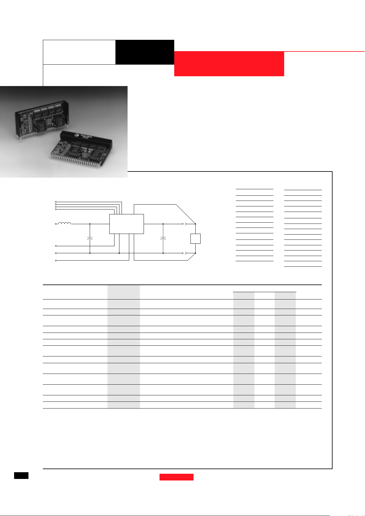
Standard Application
Cin= Required 2400µF electrolytic
C
out
= Required 2400µF electrolytic
L1 = Optional 1µH input choke
32 AMP HIGH-PERFORMANCE
“SLEDGE HAMMER” PROGRAMMABLE ISR
PT7772
The PT7772 is a new series of
high-performance, 32 Amp Integrated
Switching Regulators (ISRs) housed in
a 27-pin SIP package. The 32A capability allows easy
integration of the latest high-speed,
low-voltage µPs, ASICs, DSPs, and
bus drivers into existing 3.3V systems.
The output voltage of the PT7772
can be easily programmed from 1.3V
to 2.05V with a 4-bit input compatible
with Intel’s Pentium
Pro Processor. A
differential remote sense is also provided which automatically compensates
for any voltage drop from the ISR
to the load.
2400µF of output capacitance
are required for proper operation.
For STBY* pin; open = output enabled;
ground = output disabled.
Pin-Out Information
PT7772
7 - 11
13 - 19
20 - 25
27
V
IN
GND
1µH
GND
V
OUT
C
OUT
+
C
IN
+
12
261
L1
SYNC OUT
LOAD
REMOTE SENSE (+)
REMOTE SENSE (-)
VID1
VID2
VID3
PROGRAMMING PINS
234
STBY*
5
VID0
For assistance or to order, call (800) 531-5782
14
Power Trends, Inc. 27715 Diehl Road, Warrenville, IL 60555 (800) 531-5782 Fax: (630) 393-6902 http://www.powertrends.com
Pin Function
1 VID0
2 VID1
3 VID2
4 VID3
5 STBY*- Stand-by
6 Do not connect
7 V
in
8 V
in
9 V
in
10 V
in
11 V
in
12 Remote Sense Gnd
13 GND
Pin Function
14 GND
15 GND
16 GND
17 GND
18 GND
19 GND
20 V
out
21 V
out
22 V
out
23 V
out
24 V
out
25 V
out
26 Remote Sense V
out
27 Sync Out
Specifications
Characteristics
PT7772 SERIES
(T a = 25°C unless noted) Symbols Conditions Min Typ Max Units
Output Current I
o
Ta = +60°C, 200 LFM, pkg N 0.1
(1)
—32A
Ta = +25°C, natural convection 0.1
(1)
—26A
Input Voltage Range V
in
0.1A ≤ I
o
≤ 32A 3.1
(2)
— 3.6 V
Output Voltage Tolerance ∆V
o
V
in
= +3.3V, Io = 32A
V
o-0.03 — Vo+0.03 V
0°C ≤ Ta ≤ +55°C
Line Regulation Reg
line
3.1V ≤ V
in
≤ 3.6V, I
o
= 32A — ±10 — mV
Load Regulation Reg
load
Vin = +3.3V, 0.1 ≤ I
o
≤ 32A — ±10 — mV
Vo Ripple/Noise pk-pk V
n
V
in
= +3.3V, Io = 32A — 50 — mV
Transient Response t
tr
Io step between 16A and 32A — 100 — µSec
with C
out
= 2400µF V
os
Vo over/undershoot — 200 — mV
Efficiency η V
in
= +3.3V, Io = 20A, Vo = 1.8V — 90 — %
Switching Frequency ƒ
o
3.1V ≤ V
in
≤ 3.6V
650 700 750 kHz
0.1A ≤ I
o
≤ 32A
Absolute Maximum T
a
— 0 — +85 °C
Operating Temperature Range
Recommended Operating T
a
Forced Air Flow = 200 LFM
0 — +65 °C
Temperature Range Over V
in and Io
Ranges
Storage Temperature T
s
— -40 — +125 °C
Weight — Vertical/Horizontal — 53/66 — grams
(1) ISR-will operate down to no load with reduced specifications. Please note that this product is not short-circuit protected.
(2) The minimum input voltage is 3.1V or V
out
+1.2V, whichever is greater.
Output Capacitors:
The PT7772 series requires a minimum output capacitance of 2400µF for proper operation. Do not use Oscon type capacitors.
The maximum allowable output capacitance is 30,000µF.
Input Filter:
An input filter is optional for most applications. The input inductor must be sized to handle 32ADC with a typical value of 1µH.
The input capacitance must be rated for a minimum of 2.6Arms of ripple current. For transient or dynamic load applications, additional
capacitance may be required.
Revised 7/15/98

Ordering Information
PT7772
❏❏
❏❏
❏ = 1.3 to 2.05 Volts
Programming Information
VID3 VID2 VID1 VID0 Vout
1 1 1 1 1.30V
1 1 1 0 1.35V
1 1 0 1 1.40V
1 1 0 0 1.45V
1 0 1 1 1.50V
1 0 1 0 1.55V
1 0 0 1 1.60V
1 0 0 0 1.65V
0 1 1 1 1.70V
0 1 1 0 1.75V
0 1 0 1 1.80V
0 1 0 0 1.85V
0 0 1 1 1.90V
0 0 1 0 1.95V
0 0 0 1 2.00V
0 0 0 0 2.05V
Logic 0 = Pin 12 potential (remote sense gnd)
Logic 1 = Open circuit (no pull-up resistors)
VID3 may not be changed while the unit is operating.
For dimensions and PC board layout, see
Package Style 1020 and 1030
• +3.3V input
• 5-bit Programmable:
1.3V to 2.05V@32A
• High Efficiency
• Input Voltage Range:
3.1V to 3.6V
• Differential Remote
Sense
• 27-pin SIP Package
Features
Efficiency vs Output Current (@Vout=+1.8V)
EfEf
EfEf
Ef
ficiency (%)ficiency (%)
ficiency (%)ficiency (%)
ficiency (%)
Output CurOutput Cur
Output CurOutput Cur
Output Cur
rr
rr
r
ent (A)ent (A)
ent (A)ent (A)
ent (A)
Safe Operating Area (@Vin=+3.3V, Vout=+1.8V, Pkg N)
Output CurOutput Cur
Output CurOutput Cur
Output Cur
rr
rr
r
ent (A)ent (A)
ent (A)ent (A)
ent (A)
Ambient TAmbient T
Ambient TAmbient T
Ambient T
emperaturemperatur
emperaturemperatur
emperatur
e (°C)e (°C)
e (°C)e (°C)
e (°C)
Airflow
Recommended Maximum
Operating Temperature
Note: SOA curves represent operating conditions at
which internal components are at or below manufacturer’s
maximum rated operating temperatures.
Power Dissipation vs Output Current (@Vout=+1.8V)
Pd (WPd (W
Pd (WPd (W
Pd (W
atts)atts)
atts)atts)
atts)
Output CurOutput Cur
Output CurOutput Cur
Output Cur
rr
rr
r
ent (A)ent (A)
ent (A)ent (A)
ent (A)
Output Ripple vs Output Current (@Vout=+1.8V)
Ripple (mVpp)Ripple (mVpp)
Ripple (mVpp)Ripple (mVpp)
Ripple (mVpp)
Output CurOutput Cur
Output CurOutput Cur
Output Cur
rr
rr
r
ent (A)ent (A)
ent (A)ent (A)
ent (A)
Vin
Vin
Vin
For assistance or to order, call (800) 531-5782
15
3.3V Bus Products
DATA SHEETS
Power Trends, Inc. 27715 Diehl Road, Warrenville, IL 60555 (800) 531-5782 Fax: (630) 393-6902 http://www.powertrends.com
CHARACTERISTIC DATA
Series
PT7772
PT Series Suffix
(PT1234X)
Case/Pin
Configuration
Vertical Through-Hole N
Horizontal Through-Hole A
Horizontal Surface Mount C
60
70
80
90
100
0 4 8 12 16 20 24 28 32
4.5V
5.0V
5.5V
0
2
4
6
8
10
12
14
16
18
20
0 4 8 121620242832
4.5V
5.0V
5.5V
0
5
10
15
20
25
30
35
40
0 4 8 12 16 20 24 28 32
4.5V
5.0V
5.5V
20
30
40
50
60
70
80
90
0 4 8 12 16 20 24 28 32
Nat. Conv
60 LFM
120 LFM
200 LFM

IMPORTANT NOTICE
T exas Instruments and its subsidiaries (TI) reserve the right to make changes to their products or to discontinue
any product or service without notice, and advise customers to obtain the latest version of relevant information
to verify, before placing orders, that information being relied on is current and complete. All products are sold
subject to the terms and conditions of sale supplied at the time of order acknowledgement, including those
pertaining to warranty, patent infringement, and limitation of liability.
TI warrants performance of its semiconductor products to the specifications applicable at the time of sale in
accordance with TI’s standard warranty. Testing and other quality control techniques are utilized to the extent
TI deems necessary to support this warranty. Specific testing of all parameters of each device is not necessarily
performed, except those mandated by government requirements.
CERT AIN APPLICATIONS USING SEMICONDUCTOR PRODUCTS MAY INVOLVE POTENTIAL RISKS OF
DEATH, PERSONAL INJURY, OR SEVERE PROPERTY OR ENVIRONMENTAL DAMAGE (“CRITICAL
APPLICATIONS”). TI SEMICONDUCTOR PRODUCTS ARE NOT DESIGNED, AUTHORIZED, OR
WARRANTED TO BE SUITABLE FOR USE IN LIFE-SUPPORT DEVICES OR SYSTEMS OR OTHER
CRITICAL APPLICATIONS. INCLUSION OF TI PRODUCTS IN SUCH APPLICA TIONS IS UNDERSTOOD T O
BE FULLY AT THE CUSTOMER’S RISK.
In order to minimize risks associated with the customer’s applications, adequate design and operating
safeguards must be provided by the customer to minimize inherent or procedural hazards.
TI assumes no liability for applications assistance or customer product design. TI does not warrant or represent
that any license, either express or implied, is granted under any patent right, copyright, mask work right, or other
intellectual property right of TI covering or relating to any combination, machine, or process in which such
semiconductor products or services might be or are used. TI’s publication of information regarding any third
party’s products or services does not constitute TI’s approval, warranty or endorsement thereof.
Copyright 1999, Texas Instruments Incorporated
 Loading...