

For assistance or to order, call (800) 531-5782
Revised 1/12/99
PT7750
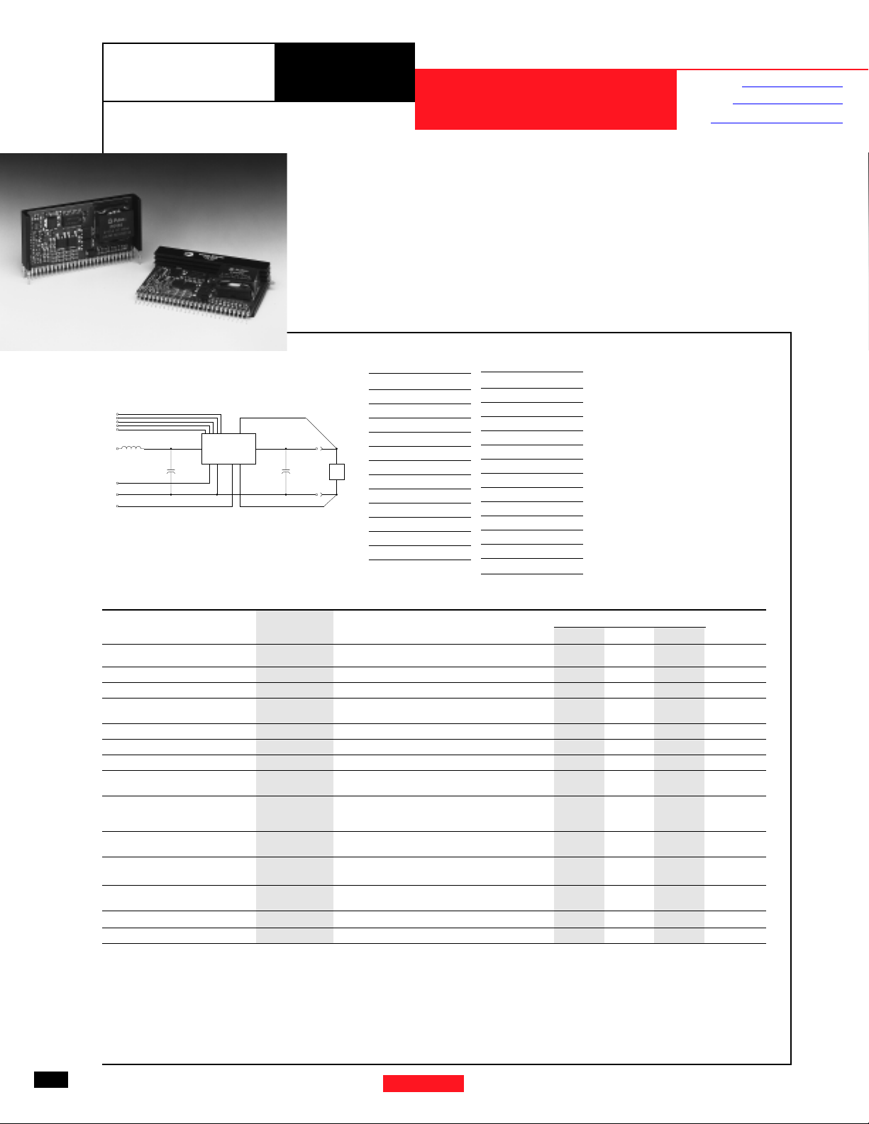
Standard Application
PROGRAMMING PINS
VID0
VID1
VID2
VID3
VID4
V
IN
SYNC OUT
GND
STBY*
L1
1µH
C
Cin= Required 560µF electrolytic
C
out
L1 = Optional 1µH input choke
6
7 - 11
27
+
IN
(See input filter note)
= Required 2000µF electrolytic
1
234
PT7750
5
13 - 19
26
12
Series
REMOTE SENSE (+)
V
20 - 25
REMOTE SENSE (-)
OUT
+
C
OUT
GND
15 AMP 24V INPUT “BIG-HAMMER III”
PROGRAMMABLE ISR
The PT7750 series is a new +24V
input, 15 Amp output, high-performance Integrated Switching Regulator
(ISR) housed in a 27-pin SIP package.
The 15A capability allows easy integration of the latest high-speed,
low-voltage µPs and bus drivers into
+24V distributed power systems.
The PT7750 series has been designed to work in parallel with one or
Pin-Out Information
Pin Function
14 GND
15 GND
16 GND
17 GND
18 GND
19 GND
20 V
21 V
22 V
23 V
24 V
25 V
26 Remote Sense V
27 Sync Out
LOAD
Pin Function
1 VID0
2 VID1
3 VID2
4 VID3
5 STBY* - Stand-by
6 VID4
7V
in
8V
in
9V
in
10 V
in
11 V
in
12 Remote Sense Gnd
13 GND
For STBY* pin:
open = output enabled
ground = output disabled.
more of the PT7747 current boosters for
increased I
in increments of 15A.
out
The output voltage of the PT7750
series can be easily programmed over a
wide range with a 5-bit input. A differential remote sense is provided which
automatically compensates for any
voltage drop from the ISR to the load.
2000µF of output capacitance is
required for proper operation.
Features
• +24V bus input
• High Efficiency
• Differential Remote
Sense
• 27-pin SIP Package
• Parallelable with
out
out
out
out
out
out
out
PT7747 15A current boosters
Mechanical Outline
Product Selector Guide
Specifications
Characteristics
(Ta = 25°C unless noted) Symbols Conditions Min Typ Max Units
Output Current I
Input Voltage Range V
Undervoltage Lockout Threshold V
Output Voltage Tolerance ∆V
Line Regulation Reg
Load Regulation Reg
Vo Ripple/Noise V
Transient Response t
with C
= 2000µF V
out
o
in
uvl
o
line
load
n
tr
os
Efficiency η V
Switching Frequency ƒ
o
Ta = +60°C, 200 LFM 0.1
Ta = +25°C, natural convection 0.1
0.1A ≤ I
≤ I
o
o max
0.1A ≤ I
≤ I
o
V
in
0°C ≤ Ta ≤ +55°C PT7756 — — ±160 mV
20V ≤ V
Vin = +24V, 0.1 ≤ I
V
in
Io step between 7.5A and 15A — 100 — µSec
Vo over/undershoot — 200 — mV
in
20V ≤ V
0.1A ≤ I
o max
= +24V, Io = 15A PT7751 — — ±80 mV
≤ 28V, I
≤ 28V
≤ 15A
= I
o
o max (w/remote sense)
≤ I
o
o max (w/remote sense)
o max
V
V
= 3.3V — 84 — %
o
= 2.5V — 80 — %
o
in
= +24V, Io = I
= +24V, Io = 10A Vo = 5.0V — 88 — %
in
o
Absolute Maximum Ta 0 — +85 °C
Operating Temperature Range
Recommended Operating T
Temperature Range At V
Storage Temperature T
a
s
Forced Air Flow = 200 LFM
= +24V, Io = 12A
in
— -40 — +125 °C
Weight — Vertical/Horizontal — 53/66 — grams
* ISR-will operate down to no load with reduced specifications. Please note that this product is not short-circuit protected.
** The PT7750 series can be easily paralleled with one or more of the PT7747 Current Boosters to provide increased output current in increments of 15A.
*** See safe operating area chart.
Output Capacitors: The PT7750 series requires a minimum output capacitance of 2000µF for proper operation. Do not use Oscon type capacitors. The maximum allowable
output capacitance is (42,000
Input Filter:
must be rated for a minimum of 8.0 Arms of ripple current when operated at maximum output current and maximum output voltage. Contact an applications engineer for input capacitor selection for applications at other output voltages and output currents.
An input inductor is optional for most applications. The input inductor must be sized to handle 9ADC with a typical value of 1µH. The input capacitance
÷
Vout)µF for the PT7751, (96,000 ÷ Vout)µF for the PT7756, or 15,000µF, whichever is less.
PT7750 SERIES
*
—15**A
*
—15**A
20.0 — 28.0 V
— 18.7 — V
— ±15 — mV
— ±10 — mV
—75—mV
300 350 400 kHz
0 — +65*** °C
Application Notes
56
Power Trends, Inc. 27715 Diehl Road, Warrenville, IL 60555 (800) 531-5782 Fax: (630) 393-6902 http://www.powertrends.com
For assistance or to order, call (800) 531-5782
SeriesPT7750
Programming Information
PT7751 PT7756
VID3 VID2 VID1 VID0 Vout Vout Vout Vout
1 1 1 1 2.5V 4.1V 6.6V 9.8V
1 1 1 0 2.6V 4.2V 6.8V 10.0V
1 1 0 1 2.7V 4.3V 7.0V 10.2V
1 1 0 0 2.8V 4.4V 7.2V 10.4V
1 0 1 1 2.9V 4.5V 7.4V 10.6V
1 0 1 0 3.0V 4.6V 7.6V 10.8V
1 0 0 1 3.1V 4.7V 7.8V 11.0V
1 0 0 0 3.2V 4.8V 8.0V 11.2V
0 1 1 1 3.3V 4.9V 8.2V 11.4V
0 1 1 0 3.4V 5.0V 8.4V 11.6V
0 1 0 1 3.5V 5.1V 8.6V 11.8V
0 1 0 0 3.6V 5.2V 8.8V 12.0V
0 0 1 1 3.7V 5.3V 9.0V 12.2V
0 0 1 0 3.8V 5.4V 9.2V 12.4V
0 0 0 1 3.9V 5.5V 9.4V 12.6V
0 0 0 0 4.0V 5.6V 9.6V 12.8V
Logic 0 = Pin 12 potential (remote sense gnd)
Logic 1 = Open circuit (no pull-up resistors)
VID3 and VID4 may not be changed while the unit is operating.
VID4=1 VID4=0 VID4=1 VID4=0
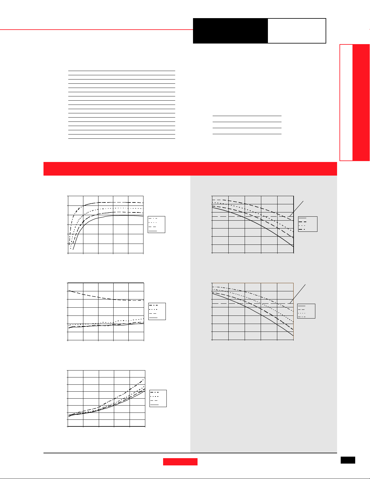
CHARACTERISTIC DATA
Efficiency vs Output Current (@Vin=+24V)
100
90
80
70
Efficiency (%)
60
50
40
03691215
Output Current (A)
Vout
12.0V
5.0V
3.3V
2.5V
Ordering Information
PT7751
PT7756
(For dimensions and PC board layout,
see Package Styles 1000 and 1010.)
PT Series Suffix
Case/Pin
Configuration
Vertical Through-Hole
Horizontal Through-Hole
Horizontal Surface Mount
PT7751 Safe Operating Area (@Vin=+24V, Over Vo Range)
90
80
70
60
50
40
Ambient Temperature (°C)
30
20
03691215
❏❏
❏ = 2.5 to 5.6 Volts
❏❏
❏❏
❏ = 6.6 to 12.8 Volts
❏❏
(PT1234X)
N
A
C
Output Current (A)
Recommended
Maximum
Operating
Temperature
Airflow
Nat conv
60LFM
120LFM
200LFM
DATA SHEETS
24V Bus Products
Ouput Ripple vs Output Current (@Vin=+24V)
70
60
50
40
30
Riplle (mV)
20
10
0
03691215
Output Current (A)
Vout
12.0V
5.0V
3.3V
2.5V
PT7756 Safe Operating Area (@Vin=+24V, Over Vo Range)
90
80
70
60
50
40
Ambient Temperature (°C)
30
20
0 3 6 9 12 15
Output Current (A)
Airflow
Power Dissipation vs Output Current (@Vin=+24V)
16
14
12
10
8
Pd (Watts)
6
4
2
0
0 3 6 9 12 15
Output Current (A)
Note: SOA curves represent operating conditions at which internal components are at or below manufacturer’s maximum rated operating temperatures.
Vout
12.0V
5.0V
3.3V
2.5V
Recommended
Maximum
Operating
Temperature
Nat conv
60LFM
120LFM
200LFM
Power Trends, Inc. 27715 Diehl Road, Warrenville, IL 60555 (800) 531-5782 Fax: (630) 393-6902 http://www.powertrends.com
57

For assistance or to order, call (800) 531-5782
Power Trends, Inc. 27715 Diehl Road, Warrenville, IL 60555 (800) 531-5782 Fax: (630) 393-6902 http://www.powertrends.com
Application Notes
Pin-Coded Output Voltage Adjustment on the
“Big Hammer III” Series ISRs
Power Trends PT7750 series ISRs incorporating pin-coded
voltage control, use pins 1, 2, 3, 4, & 6 to adjust the ouput voltage. The control pins are identified VID0 - VID4 respectively.
When the control pins are left open-circuit, the ISR output will
regulate at its factory trimmed output voltage. Each control pin
is internally connected to a precision resistor, and when
grounded increases the output voltage by a set amount. The
internal resistors are binary code weighted, allowing the output
voltage of the ISR to be programmed as a function of a binary
code. VID0 represents the LSB, and VID4 the MSB (or range
change bit). The output voltage ranges offered by these regulators are compatible with some microprocessors, and provide a
convenient method of output voltage selection for many other
applications. Refer to Figure 1 below for the connection schematic, and the PT7750 Data Sheet for the programming code
information.
Notes:
1. The programming convention is as follows:Logic 0: Connect to pin12 (Remote Sense Ground).
Logic 1: Open circuit/open drain (See notes 2, & 4)
2. Do not connect pull-up resistors to the voltage programming pins.
3. To minimize output voltage error, always use pin 12 (Remote Sense Ground) as the logic “0” reference. While the
regular ground (pins 13-19) can also be used for programming, doing so will degrade the load reglation of the
product.
PT7750 Series
More Application Notes
4. If active devices are used to ground the voltage control pins,
low-level open drain MOSFET devices should be used over
bipolar transistors. The inherent V
introduces errors in the device’s internal divider network.
Discrete transistors such as the BSS138, 2N7002,
IRLML2402, or the 74C906 hex open-drain buffer are
examples of appropriate devices.
Active Voltage Programming:
Special precautions should be taken when making changes to the
voltage control progam code while the unit is powered. It is
highly recommended that the ISR be either powered down or in
standby. Changes made to the program code while V
abled induces high current transients through the device. This is
the result of the electrolytic output capacitors being either
charged or discharged to the new output voltage set-point. The
transient current can be minimized by making only incremental
changes to the binary code, i.e. one LSB at a time. A minimum
of 100µs settling time between each program state is also recommended. Making non-incremental changes to VID3 and VID4
with the output enabled is discouraged. If they are changed, the
transients induced can overstress the device resulting in a permanent drop in efficiency. If the use of active devices prevents the
program code being asserted prior to power-up, pull pin 5
(STBY) to the device GND during the period that the input
voltage is applied to V
. Releasing pin 5 will then allow the
in
device output to execute a soft-start power-up to the programmed voltage.
(sat) in bipolar devices
ce
is en-
out
Figure 1
+24V
STBY
COM
1µH
(Optional)
Cin
6 4 3 2 1 26
VID4 - VID0
7-11
+
STBY
PT7750
Synch
Out
GND
SNS(+)
SNS(-)
20-25
VoVin
125 13-1927
Cout
+
L
O
A
D
3
 Loading...