

PT7720
7 - 11
13 - 19
20 - 25
27
V
IN
GND
1µH
GND
V
OUT
C
OUT
+
C
IN
+
12
261
L1
SYNC OUT
LOAD
REMOTE SENSE (+)
REMOTE SENSE (-)
VID1
VID2
VID3
VID4
PROGRAMMING PINS
234
STBY*
5
6
VID0
For assistance or to order, call (800) 531-5782
Power Trends, Inc. 27715 Diehl Road, Warrenville, IL 60555 (800) 531-5782 Fax: (630) 393-6902 http://www.powertrends.com
50
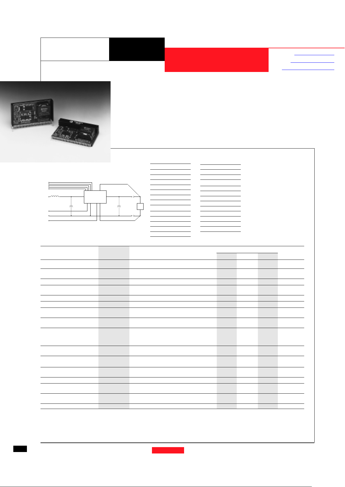
Pin-Out Information
Pin Function
1 VID0
2 VID1
3 VID2
4 VID3
5 STBY* - Stand-by
6 VID4
7V
in
8V
in
9V
in
10 V
in
11 V
in
12 Remote Sense Gnd
13 GND
14 GND
Pin Function
15 GND
16 GND
17 GND
18 GND
19 GND
20 V
out
21 V
out
22 V
out
23 V
out
24 V
out
25 V
out
26 Remote Sense V
out
27 Sync Out
Standard Application
Cin= Required 560µF electrolytic
(See input filter note)
C
out
= Required 1200µF electrolytic
L1 = Optional 1µH input choke
For STBY* pin:
open = output enabled
ground = output disabled.
• +12V bus input
• 5-bit Programmable:
1.3V to 3.5V or
4.5V to 7.6V
• High Efficiency
• Differential Remote Sense
• 27-pin SIP Package
• Parallelable with PT7748
17A current boosters
Features
Series
17 AMP 12V INPUT “BIG-HAMMER II” PROGRAMMABLE ISR
PT7720
The PT7720 series is a new +12V input,
17A output, high-performance Integrated
Switching Regulator (ISR) housed in a 27pin SIP package. The 17A capability allows
easy integration of the latest high-speed,
low-voltage µPs and bus drivers into +12V
distributed power systems.
The PT7720 series has been designed
to work in parallel with one or more of the
PT7748 current boosters for increased I
out
in increments of 17A.
The output voltage of the PT7721 can
be easily programmed from 1.3V to 3.5V
with a 5 bit input compatible with Intel’s
Pentium
IIProcessor. A differential remote sense is also provided which
automatically compensates for any voltage
drop from the ISR to the load.
1200µF of output capacitance is re-
quired for proper operation.
Output Capacitors: The PT7720 series requires a minimum output capacitance of 1200µF for proper operation. Do not use Oscon type capacitors. The maximum allowable output capacitance
Is (57,000 ÷ Vout)µF, or 15,000µF, whichever is less.
Input Filter: An input inductor is optional for most applications. The input inductor must be sized to handle 7ADC with a typical value of 1µH. The input capacitance must be rated for a
minimum of 4.0 Arms of ripple current when operated at maximum output current and maximum output voltage. Contact an applications engineer for input capacitor selection for applications
at other output voltages and output currents.
Specifications
Characteristics
PT7720 SERIES
(Ta = 25°C unless noted) Symbols Conditions Min Typ Max Units
Output Current I
o
Ta = +60°C, 200 LFM, pkg N, V
o
≤ 5V 0.1
*
—17**A
Ta = +25°C, natural convection, V
o
≤ 5V 0.1
*
—17**A
Output Power P
o
Ta = +60°C, 200 LFM, pkg N, V
o
≥ 5V — — 85 Watts
Ta = +25°C, natural convection, V
o
≥ 5V — — 85 Watts
Input Voltage Range V
in
0.1A ≤ I
o
≤ 17A 11.0 — 14.0 V
Output Voltage Tolerance ∆V
o
V
in
= +12V, Io = 17A (PT7721) Vo-0.03 — Vo+0.03 V
0°C ≤ Ta ≤ +60°C (PT7722) — ±1.0% ±2.0% % Vo
Line Regulation Reg
line
11V ≤ V
in
≤ 14V, I
o
= 17A (Using remote sense) — ±5 ±10 mV
Load Regulation Reg
load
Vin = +12V, 0.1 ≤ I
o
≤ 17A (Using remote sense) — ±5 ± 10 mV
V
o
Ripple/Noise V
n
V
in
= +12V, Io = 17A (PT7721) — 50 — mVpp
(PT7722) — 100 — mVpp
Transient Response t
tr
Io step between 7.5A and 15A — 100 — µSec
with C
out
= 1200µF V
os
Vo over/undershoot — 200 — mV
Efficiency η V
in
= +12V, Io = 10A Vo = 5.0V — 90 — %
V
o
= 3.3V — 88 — %
V
o
= 2.5V — 85 — %
V
o
= 1.5V — 78 — %
Switching Frequency ƒ
o
11V ≤ V
in
≤ 14V
300 350 400 kHz
0.1A ≤ I
o
≤ 17A
Absolute Maximum T
a
—0—+85°C
Operating Temperature Range
Recommended Operating T
a
Forced Air Flow = 200 LFM
0—+
65
***
°C
Temperature Range At V
in = 12V, Io
= 12A
Storage Temperature T
s
— -40 — +125 °C
Mechanical Shock Per Mil-STD-883D, Method 2002.3 , 1 msec,
— TBD — G’s
Half Sine, mounted to a fixture
Mechanical Vibration Per Mil-STD-883D, Method 2007.2,
20-2000 Hz, Soldered in a PC board
— TBD — G’s
Weight — Vertical/Horizontal — 51/64 — grams
* ISR-will operate down to no load with reduced specifications. Please note that this product is not short-circuit protected.
** The PT7720 series can be easily paralleled with one or more of the PT7748 Current Boosters to provide increased output current in increments of 17A.
*** See Safe Operating Area chart.
Revised 1/13/99
Application Notes
Mechanical Outline
Product Selector Guide
For assistance or to order, call (800) 531-5782
Power Trends, Inc. 27715 Diehl Road, Warrenville, IL 60555 (800) 531-5782 Fax: (630) 393-6902 http://www.powertrends.com
51
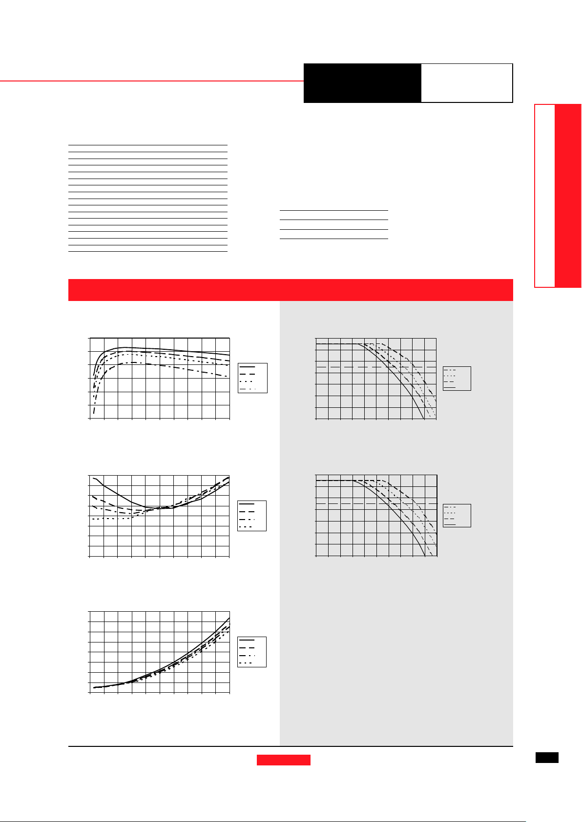
CHARACTERISTIC DATA
5V to 3.x Converters
12V Bus Products
DATA SHEETS
Programming Information
PT7721 PT7722
VID4=1 VID4=0 VID4=1 VID4=0
VID3 VID2 VID1 VID0 Vout Vout Vout Vout
1 1 1 1 2.0V 1.30V 4.5V 6.1V
1 1 1 0 2.1V 1.35V 4.6V 6.2V
1 1 0 1 2.2V 1.40V 4.7V 6.3V
1 1 0 0 2.3V 1.45V 4.8V 6.4V
1 0 1 1 2.4V 1.50V 4.9V 6.5V
1 0 1 0 2.5V 1.55V 5.0V 6.6V
1 0 0 1 2.6V 1.60V 5.1V 6.7V
1 0 0 0 2.7V 1.65V 5.2V 6.8V
0 1 1 1 2.8V 1.70V 5.3V 6.9V
0 1 1 0 2.9V 1.75V 5.4V 7.0V
0 1 0 1 3.0V 1.80V 5.5V 7.1V
0 1 0 0 3.1V 1.85V 5.6V 7.2V
0 0 1 1 3.2V 1.90V 5.7V 7.3V
0 0 1 0 3.3V 1.95V 5.8V 7.4V
0 0 0 1 3.4V 2.00V 5.9V 7.5V
0 0 0 0 3.5V 2.05V 6.0V 7.6V
Series
40
50
60
70
80
90
100
02468101214161820
5.0V
3.3V
2.5V
1.5V
Efficiency vs Output Current (@Vin=+12V)
Efficiency (%)
Output Current (A)
Safe Operating Area (@Vin=+12V, V
out
=+3.3V, Pkg N)
Output Current (A)
Ambient Temperature (°C)
Airflow
Recommended Maximum
Operating Temperature
0
2
4
6
8
10
12
14
16
0 2 4 6 8 10 12 14 16 18 20
5.0V
3.3V
2.5V
1.5V
0
2
4
6
8
10
12
14
16
0 2 4 6 8 10 12 14 16 18 20
5.0V
3.3V
2.5V
1.5V
Output Ripple vs Output Current (@Vin=+12V)
Power Dissipation vs Output Current (@Vin=+12V)
Output Current (A)
Output Current (Amps)
Ripple (mVpp)Pd (Watts)
Safe Operating Area (@Vin=+12V, V
out
=+5.0V, Pkg N)
Output Current (A)
Ambient Temperature (°C)
AirflowRecommended Maximum
Operating Temperature
Note: SOA curves represent operating conditions at which internal components are at or below manufacturer’s maximum rated operating temperatures.
PT7720
Ordering Information
PT7721
❏❏
❏❏
❏ = 1.3 to 3.5 Volts
PT7722
❏❏
❏❏
❏ = 4.5 to 7.6 Volts
(For dimensions and PC board layout,
see Package Styles 1000 and 1010.)
VV
VV
V
outout
outout
out
VV
VV
V
outout
outout
out
VV
VV
V
outout
outout
out
Logic 0 = Pin 12 potential (remote sense gnd)
Logic 1 = Open circuit (no pull-up resistors)
VID3 and VID4 may not be changed while the unit is operating.
PT Series Suffix
(PT1234X)
Case/Pin
Configuration
Vertical Through-Hole
N
Horizontal Through-Hole
A
Horizontal Surface Mount
C
20
30
40
50
60
70
80
90
0 2 4 6 8101214161820
200LFM
120LFM
60LFM
Nat conv
20
30
40
50
60
70
80
90
0 2 4 6 8 101214161820
200LFM
120LFM
60LFM
Nat conv

For assistance or to order, call (800) 531-5782
3
Power Trends, Inc. 27715 Diehl Road, Warrenville, IL 60555 (800) 531-5782 Fax: (630) 393-6902 http://www.powertrends.com
Application Notes
PT7720 Series
More Application Notes
Pin-Coded Output Voltage Adjustment on the
“Big Hammer II” Series ISRs
Power Trends PT7720 series ISRs incorporate pin-coded voltage control to adjust the ouput voltage. The control pins are
identified VID0 - VID4 (pins 1, 2, 3, 4, & 6) respectively.
When the control pins are left open-circuit, the ISR output will
regulate at its factory trimmed output voltage. Each pin is internally connected to a precision resistor, which when grounded
changes the output voltage by a set amount. By selectively
grounding VID0 -VID4, the output voltage of each ISR in the
PT7720 series ISRs can be programmed in incremental steps
over its specified output voltage range. The output voltage
ranges offered by these regulators provide a convenient method
of output voltage selection for many applications. In addition,
the program code and output voltage range of the PT7721
model ISR is compatible with the voltage ID specification defined by Intel Corporation for voltage regulator modules
(VRMs) used to power Pentium® microprocessors. Refer to
Figure 1 below for the connection schematic, and the PT7720
Data Sheet for the appropriate programming code information.
Notes:
1. The programming convention is as follows:Logic 0: Connect to pin12 (Remote Sense Ground).
Logic 1: Open circuit/open drain (See notes 2, & 4)
2. Do not connect pull-up resistors to the voltage programming pins.
3. To minimize output voltage error, always use pin 12 (Remote Sense Ground) as the logic “0” reference. While the
regular ground (pins 13-19) can also be used for program-
Figure 1
ming, doing so will degrade the load reglation of the product.
4. If active devices are used to ground the voltage control pins,
low-level open drain MOSFET devices should be used over
bipolar transistors. The inherent V
ce
(sat) in bipolar devices
introduces errors in the device’s internal divider network.
Discrete transistors such as the BSS138, 2N7002,
IRLML2402, or the 74C906 hex open-drain buffer are
examples of appropriate devices.
Active Voltage Programming:
Special precautions should be taken when making changes to the
voltage control progam code while the unit is powered. It is
highly recommended that the ISR be either powered down or
held in standby. Changes made to the program code while V
out
is enabled induces high current transients through the device.
This is the result of the electrolytic output capacitors being either charged or discharged to the new output voltage set-point.
The transient current can be minimized by making only incremental changes to the binary code, i.e. one LSB at a time. A
minimum of 100µs settling time between each program state is
also recommended. Making non-incremental changes to VID3
and VID4 with the output enabled is discouraged. If they are
changed, the transients induced can overstress the device resulting in a permanent drop in efficiency. If the use of active devices
prevents the program code being asserted prior to power-up,
pull pin 5 (STBY) to the device GND during the period that the
input voltage is applied to V
in
. Releasing pin 5 will then allow
the device output to execute a soft-start power-up to the programmed voltage.
Cout
+
Cin
+
1µH
(Optional)
+12V
COM
STBY
L
O
A
D
PT7720
6 4 3 2 1 26
20-25
125 13-1927
7-11
VoVin
GND
SNS(+)
SNS(-)
Synch
Out
STBY
VID4 - VID0

IMPORTANT NOTICE
T exas Instruments and its subsidiaries (TI) reserve the right to make changes to their products or to discontinue
any product or service without notice, and advise customers to obtain the latest version of relevant information
to verify, before placing orders, that information being relied on is current and complete. All products are sold
subject to the terms and conditions of sale supplied at the time of order acknowledgement, including those
pertaining to warranty, patent infringement, and limitation of liability.
TI warrants performance of its semiconductor products to the specifications applicable at the time of sale in
accordance with TI’s standard warranty. Testing and other quality control techniques are utilized to the extent
TI deems necessary to support this warranty. Specific testing of all parameters of each device is not necessarily
performed, except those mandated by government requirements.
CERT AIN APPLICATIONS USING SEMICONDUCTOR PRODUCTS MAY INVOLVE POTENTIAL RISKS OF
DEATH, PERSONAL INJURY, OR SEVERE PROPERTY OR ENVIRONMENTAL DAMAGE (“CRITICAL
APPLICATIONS”). TI SEMICONDUCTOR PRODUCTS ARE NOT DESIGNED, AUTHORIZED, OR
WARRANTED TO BE SUITABLE FOR USE IN LIFE-SUPPORT DEVICES OR SYSTEMS OR OTHER
CRITICAL APPLICATIONS. INCLUSION OF TI PRODUCTS IN SUCH APPLICA TIONS IS UNDERSTOOD T O
BE FULLY AT THE CUSTOMER’S RISK.
In order to minimize risks associated with the customer’s applications, adequate design and operating
safeguards must be provided by the customer to minimize inherent or procedural hazards.
TI assumes no liability for applications assistance or customer product design. TI does not warrant or represent
that any license, either express or implied, is granted under any patent right, copyright, mask work right, or other
intellectual property right of TI covering or relating to any combination, machine, or process in which such
semiconductor products or services might be or are used. TI’s publication of information regarding any third
party’s products or services does not constitute TI’s approval, warranty or endorsement thereof.
Copyright 1999, Texas Instruments Incorporated
 Loading...