

Texas Instruments PT6931N, PT6932A, PT6932C, PT6932N, PT6931A Datasheet
...
For assistance or to order, call (800) 531-5782
Power Trends, Inc. 27715 Diehl Road, Warrenville, IL 60555 (800) 531-5782 Fax: (630) 393-6902 http://www.powertrends.com
PT6930 Series
Standard Application
5V TO 3.3V/2.5V 25 WATT DUAL OUTPUT
INTEGRATED SWITCHING REGULATOR
Ordering Information
PT6931
❏❏
❏❏
❏ = +3.3 Volts
+2.5/+1.8 Volts
PT6932
❏❏
❏❏
❏ = +3.3 Volts
+1.5 Volts
C1 = Req’d 560µF electrolytic
(1)
C2 = Req’d 330µF electrolytic
(1)
C3 = Optional 100µF electrolytic
Features
• Dual Outputs:
+3.3V/6A
+2.5V/2.2A or +1.8V/1.5A
• Adjustable Output Voltage
• Remote Sense (both outputs)
• Standby Function
• Over-Temperature Protection
• Soft-Start
• Internal Sequencing
• 23-pin Excalibur™ Package
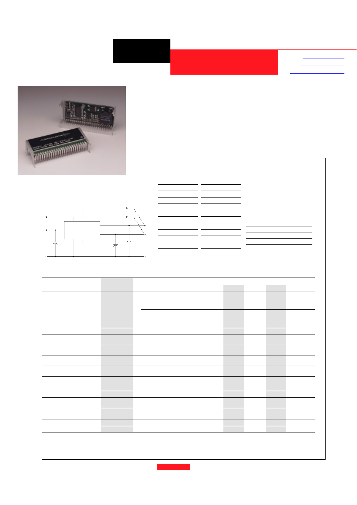
Pin Function
1V
1
Remote Sense
2 Do Not Connect
3 STBY
4V
in
5V
in
6V
in
7 GND
8 GND
9 GND
10 GND
11 GND
12 V
1out
Pin Function
13 V
1out
14 V
1out
15 V
1out
16 V
1
Adjust
17 Do Not Connect
18 V
2out
19 V
2out
20 V
2out
21 V
2out
22 V
2
Remote Sense
23 V
2
Adjust*
Pin-Out Information
The PT6930 is a new series of 25W
dual output ISRs designed to power the
latest generation DSP chips. Both output
voltages are independently adjustable
with external resistors. In addition, the
second output voltage of the PT6931 can
be selected for either 2.5V or 1.8V to
accommodate the next generation of
DSP chips. The internal power
sequencing of both outputs meet the
requirements of TI’s ‘C6000 series DSPs.
(For dimensions and PC board layout,
see Package Styles 1320 and 1330.)
PT6930
C2
+
GND
V
IN
GND
4,5,6
7-11
12-15
18-21
16
C1
22
C3
+
23
1
3
STBY
V2
SENSE
V1
SENSE
V1
OUT
V2
OUT
PT Series Suffix
(PT1234X)
Case/Pin
Configuration
Vertical Through-Hole
N
Horizontal Through-Hole
A
Horizontal Surface Mount
C
*Note: for PT6931 only:
with pin 23 open, V2out=2.5V
with pin 23 shorted to pin 22, V2out=1.8V
SLTS062 - DECEMBER 1999
Application Notes
Mechanical Outline
Product Selector Guide
Patent pending on package assembly
New Space-Saving Package
Preliminary Specifications
Characteristics
PT6930 SERIES
(Ta= 25°C unless noted) Symbols Conditions Min Typ Max Units
Output Current I
o
T
a
= +60°C, 200 LFM, pkg N V
1
= 3.3V 0.1
(2)
—5.5
(3)
V
2
= 2.5V 0 — 2.2
(3)
A
V
2
= 1.8V 0 — 1.75
(3)
V
2
= 1.2V 0 — 1.2
(3)
T
a
= +25°C, natural convection V
1
= 3.3V 0.1 — 6.0
V
2
= 2.5V 0 — 2.2
A
V
2
= 1.8V 0 — 1.75
V
2
= 1.2V 0 — 1.2
Input Voltage Range V
in
0.1A ≤ I
o
≤ I
max
4.5 — 5.5 V
Output Voltage Tolerance ∆V
o
V
in
= +5V, Io = I
max,
both outputs
V
o-0.1 — Vo+0.1 V
0°C ≤ Ta ≤ +65°C
Line Regulation Reg
line
4.5V ≤ V
in
≤ 5.5V, I
o
= I
max
V
1
= 3.3V — ±7 ±17
mV
V
2
= 2.5V — ± 7 ±13
Load Regulation Reg
load
V
in
= +5V, 0.1 ≤ I
o
≤ I
max
V
1
= 3.3V — ±17 ±33
mV
V
2
= 2.5V — ± 4 ±10
Vo Ripple/Noise V
n
V
in
= +5V, Io = I
max
V
1
= 3.3V — 50 —
mV
V
2
= 2.5V — 2 5 —
Transient Response t
tr
Io step between 0.5xI
max
and I
max
— 25 — µSec
with C
2
= 330µF V
os
Vo over/undershoot V
1
= 3.3V — 60 —
mV
V
2
= 2.5V — 6 0 —
Efficiency η V
in
= +5V, Io = 4A total — 75 — %
Switching Frequency ƒ
o
4.5V ≤ V
in
≤ 5.5V
475
600 725
kHz
0.1A ≤ I
o
≤ I
max
Absolute Maximum T
a
—
-40
(4)
— +85
(5)
°C
Operating Temperature Range
Storage Temperature T
s
— -40 — +125 °C
Weight — Vertical/Horizontal — 29 — grams
Notes:
(1) The PT6930 series requires a 560µF electrolytic capacitor on the input and a 330µF electrolytic capacitor on the output for proper operation in all applications.
(2) I
o
min current of 0.25A can be divided btween both outputs; V1, or V2. The ISR will operate down to no-load with reduced specifications.
(3) I
o
max listed for each output assumes the maximum current drawn simultaneously on both outputs. Consult the factory for the absolute maximum.
(4) For operating temperatures below 0°C, use tantalum type capacitors on both the input and output.
(5) See Safe Operating Area curves for appropriate derating.
For assistance or to order, call (800) 531-5782
Power Trends, Inc. 27715 Diehl Road, Warrenville, IL 60555 (800) 531-5782 Fax: (630) 393-6902 http://www.powertrends.com
CHARACTERISTIC DATA
20.0
30.0
40.0
50.0
60.0
70.0
80.0
90.0
0.0 1.0 2.0 3.0 4.0 5.0 6.0
Output Current (A)
Ambient Temperature ( C)
200LFM
120LFM
60LFM
Nat conv
Airflow
PT6930 Series
Note:Note:
Note:Note:
Note: All data listed in the above graphs has been developed from actual products tested at 25°C. This data is considered typical data for the ISR.
PT6931, V2out = 2.5V , I2out = 2.2A (See Foot Note)
Total Efficiency vs I1out
Total Power Dissipation vs I1out
Safe Operating Area vs I1out
V1out Ripple vs I1out
40
50
60
70
80
90
0123456
Output Current (A)
Efficiency (%)
4.5V
5.0V
5.5V
Vin
0
10
20
30
40
0123456
Output Current (A)
Ripple (mV)
5.5V
5.0V
4.5V
Vin
0
2
4
6
8
0123456
Output Current (A)
PDiss (Watts)
5.5V
5.0V
4.5V
Vin
 Loading...