

Page 1
For assistance or to order, call (800) 531-5782
Power Trends, Inc. 27715 Diehl Road, Warrenville, IL 60555 (800) 531-5782 Fax: (630) 393-6902 http://www.powertrends.com
28
Application Notes
Mechanical Outline
Product Selector Guide
PT6900 Series
Standard Application
12 WATT PLUS TO MINUS VOLTAGE
CONVERTER
Ordering Information
PT6901
❏❏
❏❏
❏ = -2.0 Volts
PT6902
❏❏
❏❏
❏ = -5.2 Volts
Cin= Required 330µF electrolytic
C
out
= Required 330µF electrolytic
Features
• Single-Device: +5V input
• Remote Sense
• Input Voltage Range:
4.75V to 5.5V
• Adjustable Output Voltage
• 23-pin SIP Package
Pin Function
1 Do not connect
2V
out
Adjust
3V
in
4V
in
5V
in
6V
in
7V
in
8 Remote Sense GND
9 GND
10 GND
11 GND
12 GND
Pin Function
13 GND
14 GND
15 GND
16 V
out
17 V
out
18 V
out
19 V
out
20 V
out
21 V
out
22 Remote Sense V
out
23 Do not connect
Pin-Out Information
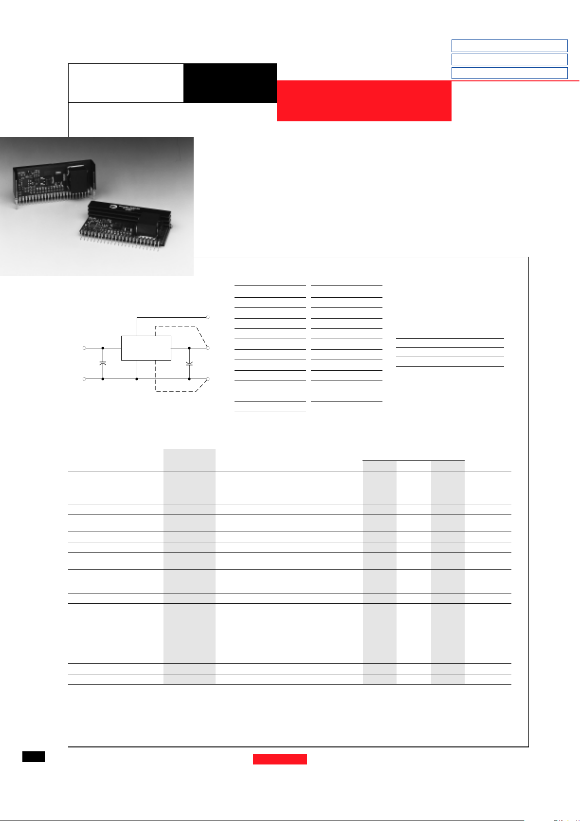
The PT6900 is a new series of plus to
minus high- performance, 12 watt voltage
converters housed in a 23-pin SIP package.
The PT6900 is designed to supply
regulated negative voltages for powering the latest ECL (-5.2V) and
GaAs (-2.0V) ICs used in high-speed
fiber optic communications. A 330µF
electrolytic capacitor is required on the
input and output for proper operation.
(For dimensions and PC board layout,
see Package Styles 1100 and 1110.)
CoutCin
PT6900
16-21
9-15
3-7
2
V
ADJ
-V
OUT
GNDGND
+V
IN
+
+
22
Remote Sense
Remote Sense
8
PT Series Suffix
(PT1234X)
Case/Pin
Configuration
Vertical Through-Hole
N
Horizontal Through-Hole
A
Horizontal Surface Mount
C
Specifications
Characteristics
PT6900 SERIES
(Ta= 25°C unless noted) Symbols Conditions Min Typ Max Units
Output Current I
o
Ta = +60°C, 200 LFM, pkg N V
o
= -2.0V 0.1
*
—6 A
V
o
= -5.2V 0.1
*
— 2.5 A
T
a
= +25°C, natural convection V
o
= -2.0V 0.1
*
—6 A
V
o
= -5.2V 0.1
*
— 2.5 A
Input Voltage Range V
in
0.1A ≤ I
o
≤ I
max
4.75 — 5.5 V
Output Voltage Tolerance ∆V
o
V
in
= +5V, Io = I
max
Vo-0.05 — Vo+0.05 V
0°C ≤ Ta ≤ +60°C
Line Regulation Reg
line
4.75V ≤ V
in
≤ 5.5V, I
o
= I
max
— ±0.5 ±1.0 %
Load Regulation Reg
load
Vin = +5V, 0.1 ≤ I
o
≤ I
max
— ±0.5 ±1.0 %
V
o
Ripple/Noise V
n
V
in
= +5V, Io = I
max
V
o
= -2.0V — 40 — mV
V
o
= -5.2V — 10 0 — mV
Transient Response t
tr
Io step between 0.5xI
max
and I
max
— 100 — µSec
with C
out
= 330µF V
os
Vo over/undershoot V
o
= -2.0V — 10 0 — mV
V
o
= -5.2V — 20 0 — mV
Efficiency η V
in
= +5V, Io = 0.5xI
max,
V
o
= -2.0V — 70 — %
Switching Frequency ƒ
o
4.75V ≤ V
in
≤ 5.5V
500
——
kHz
0.1A ≤ I
o
≤ I
max
Absolute Maximum T
a
— 0 — +85 °C
Operating Temperature Range
Recommended Operating T
a
Forced airflow = 200 LFM
0 — +60 °C
Temperature Range Over V
in and Io
Ranges
Storage Temperature T
s
— -40 — +125 °C
Weight — Vertical/Horizontal — 28/33 — grams
* ISR-will operate down to no load with reduced specifications. Please note that this product is not short-circuit protected.
Revised 11/12/98
Note: Case must be connected to
ground pins for proper operation
Page 2
For assistance or to order, call (800) 531-5782
Power Trends, Inc. 27715 Diehl Road, Warrenville, IL 60555 (800) 531-5782 Fax: (630) 393-6902 http://www.powertrends.com
29
5V to 3.x Converters
5V Bus Products
DATA SHEETS
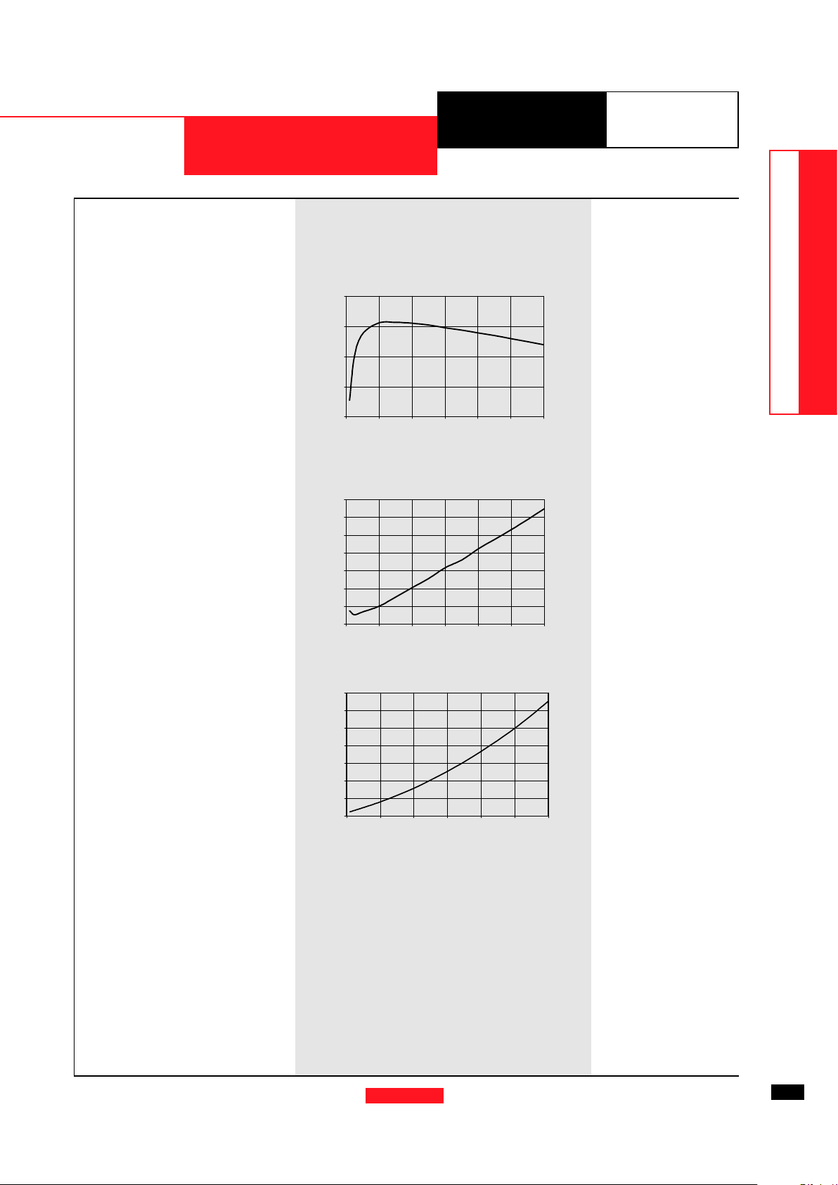
CHARACTERISTIC DATA
PT6900 Series
Efficiency vs Output Current (@Vin=+5V)
Ripple vs Output Current (@Vin=+5V)
0
5
10
15
20
25
30
35
0123456
40
50
60
70
80
0123456
PT6901, -2.0 VDC
0
1
2
3
4
5
6
7
0123456
Power Dissipation vs Output Current
PD-(Watts) Ripple-(mV)
Iout-(Amps)
Iout-(Amps)
Iout-(Amps)
Efficiency - %
Page 3

For assistance or to order, call (800) 531-5782
3
Power Trends, Inc. 27715 Diehl Road, Warrenville, IL 60555 (800) 531-5782 Fax: (630) 393-6902 http://www.powertrends.com
Application Notes
PT6900 Series
More Application Notes
Adjusting the Output Voltage of the
PT6900 Positive to Negative Converter Series
The negative output voltage of the Power Trends PT6900 Series ISRs may be adjusted higher or lower than the factory
trimmed pre-set voltage with the addition of a single external
resistor. Table 1 accordingly gives the allowable adjustment
range for each model in the series as Va (min) and Va (max).
Adjust Up: An increase in the output voltage is obtained by
adding a resistor R2, between pin 2 (V
o
adjust) and pin 8
(Remote Sense GND).
Adjust Down: Add a resistor (R1), between pin 2 (V
o
adjust) and
pin 22 (Remote Sense V
o
).
Refer to Figure 1 and Table 2 for both the placement and value
of the required resistor, either (R1) or R2 as appropriate.
Notes:
1. Use only a single 1% resistor in either the (R1) or R2 location. Place the resistor as close to the ISR as possible.
2. Never connect capacitors from V
o
adjust to either GND,
V
out
, or the Sense pins. Any capacitance added to the
Vo adjust pin will affect the stability of the ISR.
3. If the sense pins are not being used, the resistors (R1) and R2
can be connected to V
out
and GND respectively.
4. An increase in the output voltage must be accompanied by a
corresponding reduction in the maximum output current.
The revised maximum output current must be reduced to
the equivalent of 12Watts.
i.e.
I
out
(max) =
12
Adc,
V
a
where Va is the adjusted output voltage.
Figure 1
The respective values of (R1) [adjust down], and R2 [adjust up],
can also be calculated using the following formulae.
(R1) =
24.9 (2V
a
– Vo)
– R
s
kΩ
2(V
o
– Va)
R2 =
24.9 V
o
– R
s
kΩ
2(Va – Vo)
Where: V
o
= Original output voltage
V
a
= Adjusted output voltage
R
s
= The resistance given in Table 1
Table1
PT6900 ADJUSTMENT RANGE AND FORMULA PARAMETERS
Series Pt # PT6903 PT6901 PT6902
Vo (nom) -1.5V -2.0V -5.2V
Va (min) -1.1V -1.4V -3.7V
Va (max) -2.9V -4.4V -8.9V
Rs (k
ΩΩ
ΩΩ
Ω) 12.7 10.0 17.4
C
in
330µF
+
C
out
330µF
+
R2
(Up)
(R1)
(Down)
COMCOM
Vout(-)+Vin
PT6900
16 - 21
29 - 15
3 - 7
+Vin -Vo
GND Vo(adj)
Vo(sense)
22
8
GND(sense)
L
O
A
D
Page 4

For assistance or to order, call (800) 531-5782
4
Application
Power Trends, Inc. 27715 Diehl Road, Warrenville, IL 60555 (800) 531-5782 Fax: (630) 393-6902 http://www.powertrends.com
Notes
PT6900 Series
PT6900 ADJUSTMENT RESISTOR VALUES
Series Pt # PT6903 PT6901 PT6902
Current 6Adc 6Adc 2.5Adc
Vo (nom) –1.5Vdc –2.0Vdc –5.2Vdc
Va (req’d)
–1.1 (9.1)kΩ
–1.2 (24.7)kΩ
–1.3 (55.8)kΩ
–1.4 (149.0)kΩ (6.6)kΩ
–1.5 (14.9)kΩ
–1.6 174.0kΩ (27.4)kΩ
–1.7 80.7kΩ (48.1)kΩ
–1.8 49.6kΩ (89.6)kΩ
–1.9 34.0kΩ (214.0)kΩ
–2.0 24.7kΩ
–2.1 18.4kΩ 239.0kΩ
–2.2 14.0kΩ 115.0kΩ
–2.3 10.6kΩ 73.0kΩ
–2.4 8.1kΩ 52.3kΩ
–2.5 6.0kΩ 39.8kΩ
–2.6 4.3kΩ 31.5kΩ
–2.7 2.9kΩ 25.6kΩ
–2.8 1.7kΩ 21.1kΩ
–2.9 0.6kΩ 17.7kΩ
–3.0 14.9kΩ
–3.1 12.6kΩ
–3.2 10.8kΩ
–3.3 9.2kΩ
–3.4 7.8kΩ
–3.5 6.6kΩ
–3.6 5.6kΩ
–3.7 4.7kΩ (0.9)kΩ
–3.8 3.8kΩ (3.9)kΩ
–3.9 3.1kΩ (7.5)kΩ
–4.0 2.5kΩ (11.7)kΩ
–4.1 1.9kΩ (16.6)kΩ
–4.2 1.3kΩ (22.4)kΩ
–4.3 0.8kΩ (29.6)kΩ
–4.4 0.4kΩ (38.6)kΩ
Series Pt # PT6903 PT6901 PT6902
Current 6Adc 6Adc 2.5Adc
Vo (nom) –1.5Vdc –2.0Vdc –5.2Vdc
Va (req’d)
–4.5 (50.2)kΩ
–4.6 (65.6)kΩ
–4.7 (87.2)kΩ
–4.8 (120.0)kΩ
–4.9 (174.0)kΩ
–5.0 (281.0)kΩ
–5.1 (605.0)kΩ
–5.2
–5.3 630.0kΩ
–5.4 306.0kΩ
–5.5 198.0kΩ
–5.6 144.0kΩ
–5.7 112.0kΩ
–5.8 90.5kΩ
–5.9 75.1kΩ
–6.0 63.5kΩ
–6.2 47.3kΩ
–6.4 36.5kΩ
–6.6 28.8kΩ
–6.8 23.1kΩ
–7.0 18.6kΩ
–7.2 15.0kΩ
–7.4 12.0kΩ
–7.6 9.6kΩ
–7.8 7.5kΩ
–8.0 5.7kΩ
–8.2 4.2kΩ
–8.5 2.2kΩ
–8.9 0.1kΩ
Table 2
R1 = (Red) R2 = Black
Page 5

IMPORTANT NOTICE
T exas Instruments and its subsidiaries (TI) reserve the right to make changes to their products or to discontinue
any product or service without notice, and advise customers to obtain the latest version of relevant information
to verify, before placing orders, that information being relied on is current and complete. All products are sold
subject to the terms and conditions of sale supplied at the time of order acknowledgement, including those
pertaining to warranty, patent infringement, and limitation of liability.
TI warrants performance of its semiconductor products to the specifications applicable at the time of sale in
accordance with TI’s standard warranty. Testing and other quality control techniques are utilized to the extent
TI deems necessary to support this warranty. Specific testing of all parameters of each device is not necessarily
performed, except those mandated by government requirements.
CERT AIN APPLICATIONS USING SEMICONDUCTOR PRODUCTS MAY INVOLVE POTENTIAL RISKS OF
DEATH, PERSONAL INJURY, OR SEVERE PROPERTY OR ENVIRONMENTAL DAMAGE (“CRITICAL
APPLICATIONS”). TI SEMICONDUCTOR PRODUCTS ARE NOT DESIGNED, AUTHORIZED, OR
WARRANTED TO BE SUITABLE FOR USE IN LIFE-SUPPORT DEVICES OR SYSTEMS OR OTHER
CRITICAL APPLICATIONS. INCLUSION OF TI PRODUCTS IN SUCH APPLICA TIONS IS UNDERSTOOD T O
BE FULLY AT THE CUSTOMER’S RISK.
In order to minimize risks associated with the customer’s applications, adequate design and operating
safeguards must be provided by the customer to minimize inherent or procedural hazards.
TI assumes no liability for applications assistance or customer product design. TI does not warrant or represent
that any license, either express or implied, is granted under any patent right, copyright, mask work right, or other
intellectual property right of TI covering or relating to any combination, machine, or process in which such
semiconductor products or services might be or are used. TI’s publication of information regarding any third
party’s products or services does not constitute TI’s approval, warranty or endorsement thereof.
Copyright 1999, Texas Instruments Incorporated
 Loading...