

For assistance or to order, call (800) 531-5782
54
Power Trends, Inc. 27715 Diehl Road, Warrenville, IL 60555 (800) 531-5782 Fax: (630) 393-6902 http://www.powertrends.com
• Single Device: 5A Output
• Input Voltage Range: 9V to 28V
• Adjustable Output Voltage
• 80% Efficiency
• Remote Sense Capability
• Standby Function
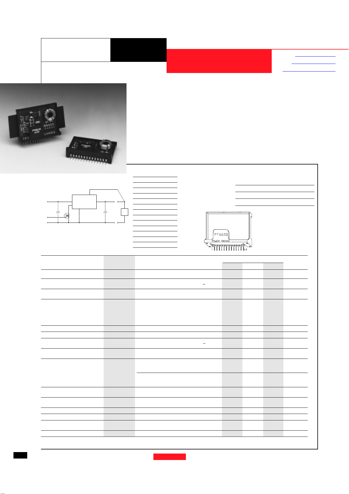
The PT6650 series is a new addition to Power Trends’ line of 24V bus
Integrated Switching Regulators
5 AMP 24V INPUT
INTEGRATED SWITCHING REGULATOR
PT6650 Series
Standard Application
C1 = Required 100µF electrolytic
C2 = Required 330µF electrolytic
Q1= NFET-or Open Collector Gate
PT6650
4,5,6
7,8,9,10
11,12,13
V
IN
COM
COM
V
OUT
C
2
+
C
1
+
1
3
STBY
Q
1
REMOTE SENSE
LOAD
Ordering Information
PT6651¨ = +3.3 Volts
PT6652¨ = +2.5 Volts
PT6653¨ = +5.0 Volts
PT6654¨ = +9.0 Volts
PT6655¨ = +15.0 Volts
PT6656¨ = +12.0 Volts
PT Series Suffix
(PT1234X)
Case/Pin Heat Heat Spreader
Configuration Spreader with Side Tabs
Vertical Through-Hole
PR
Horizontal Through-Hole
DG
Horizontal Surface Mount
EB
1 Remote Sense
2 Do Not Connect
3 STBY*- Standby
4V
in
5V
in
6V
in
7 GND
8 GND
9 GND
10 GND
11 V
out
12 V
out
13 V
out
14 V
out
Adjust
Pin-Out Information
(ISRs). Designed for general purpose
industrial applications requiring as
much as 5A of output current, the
PT6650 is packaged in a 14-Pin SIP
(Single In-line Package) and is available
in a surface-mount configuration.
Only two external capacitors are
required for proper operation. Please
note that this product does not include
short circuit protection.
Note: Back surface
of product is
conducting metal
54
Pkg Style 400
Specifications
Characteristics
PT6650 SERIES
(Ta = 25°C unless noted) Symbols Conditions Min Typ Max Units
Output Current I
o
Ta = 60°C, 200 LFM, pkg P 0.1* — 5.0** A
Ta = 25°C, natural convection 0.1* — 5.0** A
Input Voltage Range V
in
0.1A ≤ I
o
≤ 5.0A Vo < +6V +9V — +28V V
V
o
> +6V Vo+3 — +28V V
Output Voltage Tolerance ∆V
o
Over V
in
range
Ta = -40°C to +65°C
V
o-0.1 — Vo+0.1 V
Output Voltage Adjust Range V
oadj
Pin 14 to V
o
or ground Vo = +3.3V 2.2 — 4.7
V
o
= +2.5V 1.8 — 4.3
V
o
= +5.0V 3.0 — 6.5 V
V
o
= +9.0V 6.0 — 10.2
V
o
= +12V 9.0 — 13.6
V
o
= +15V 10.0 — 17.0
Line Regulation Reg
line
+9V≤Vin≤+28V, Io = 5.0A — ±0.5 ±1.0 %V
o
Load Regulation Reg
load
Vin = +24V, 0.1≤ Io≤5.0A — ±0.5 ±1.0 %V
o
Vo Ripple/Noise V
n
V
in
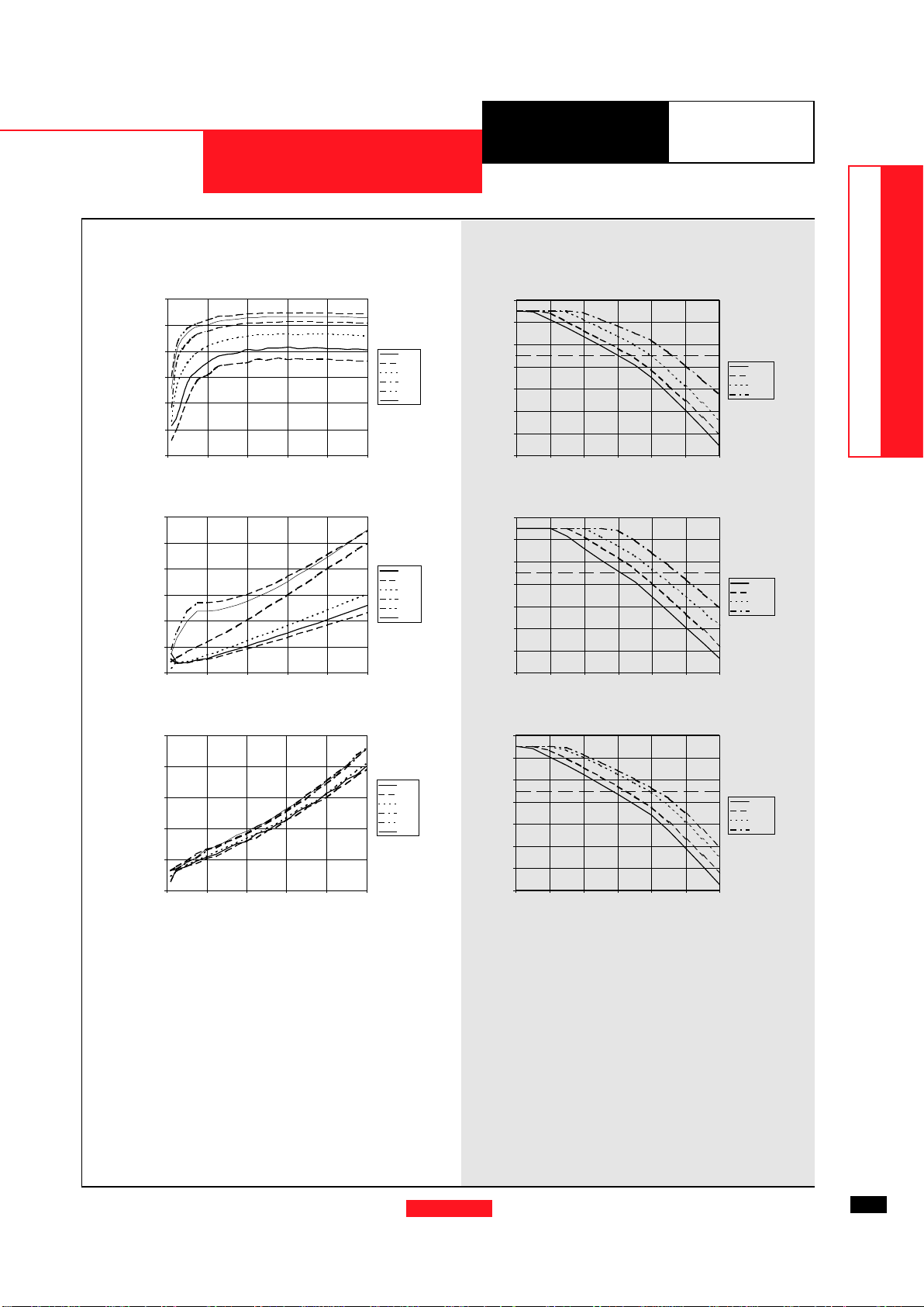
= +24V, Io = 5.0A Vo < +6V — 50 — mVpp
V
o
> +6V 1.0 %V
o
Transient Response t
tr
Io step between 2.5A and 5.0A — 100 — µSec
with C2 = 330µF V
os
Vo over/undershoot — 100 — mV
Efficiency
η Vin = +24V, Io = 0.5x I
o maxVo
= +3.3V — 81 — %
V
o
= +2.5V — 76 — %
V
o
= +5.0V — 85 — %
V
in
= +24V, Io = I
o max
V
o
= +3.3V — 80 — %
V
o
= +2.5V — 75 — %
V
o
= +5.0V — 84 — %
Switching Frequency ƒ
o
9V ≤ V
in
≤ 28V
500 550 600 kHz
Over Io range
Recommended Operating T
a
Free Air Convection (40-60 LFM)
-40 — +65 °C
Temperature Range Over V
in
and Io ranges with heat tab
Storage Temperature T
s
— -40 — +125 °C
Mechanical Shock — Per Mil-STD-883D, Method 2002.3 — 500 — G’s
Mechanical Vibration — Per Mil-STD-883D, Method 2007.2,
— 7.5 — G’s
20-2000 Hz, soldered in a PC board
Weight — — — 14 — grams
* ISR will operate down to no load with reduced specifications. ** See SOA curves.
Note:
The PT6650 Series requires a 330µF(output) and 100µF(input) electrolytic capacitors for proper operation in all applications.
Revised 2/5/99
Application Notes
Mechanical Outline
Product Selector Guide
For assistance or to order, call (800) 531-5782
55
24V Bus Products
DATA SHEETS
Power Trends, Inc. 27715 Diehl Road, Warrenville, IL 60555 (800) 531-5782 Fax: (630) 393-6902 http://www.powertrends.com
CHARACTERISTIC DATA
55
24V Bus Products
DATA SHEETS
PT6650 Series
Efficiency vs Output Current
Ripple vs Output Current
Power Dissipation vs Output Current
Efficiency (%)
Output Current (A)
Ripple (mVpp)
Output Current (A)
Pd (Watts)
Output Current (A)
PT6650 Series @VPT6650 Series @V
PT6650 Series @VPT6650 Series @V
PT6650 Series @V
in=+24Vin=+24V
in=+24Vin=+24V
in=+24V
Safe Operating Area Curves @VSafe Operating Area Curves @V
Safe Operating Area Curves @VSafe Operating Area Curves @V
Safe Operating Area Curves @V
in=+24Vin=+24V
in=+24Vin=+24V
in=+24V
40
50
60
70
80
90
100
012345
PT6651
PT6652
PT6653
PT6654
PT6655
PT6656
0
20
40
60
80
100
120
012345
PT6651
PT6652
PT6653
PT6654
PT6655
PT6656
0
1
2
3
4
5
012345
PT6651
PT6652
PT6653
PT6654
PT6655
PT6656
PT6651P, 3.3V
Ambient Temperature (°C)
Output Current (A)
Airflow
Recommended Maximum
Operating Temperature
Ambient Temperature (°C)
Output Current (A)
Airflow
Recommended Maximum
Operating Temperature
PT6652P, 2.5V
Ambient Temperature (°C)
Output Current (A)
Airflow
Recommended Maximum
Operating Temperature
PT6653P, 5.0V
20
30
40
50
60
70
80
90
0123456
Nat conv
60LFM
120LFM
200LFM
20
30
40
50
60
70
80
90
0123456
Nat co nv
60LFM
120LFM
200LFM
20
30
40
50
60
70
80
90
0123456
Nat conv
60LFM
120LFM
200LFM

For assistance or to order, call (800) 531-5782
3
Power Trends, Inc. 27715 Diehl Road, Warrenville, IL 60555 (800) 531-5782 Fax: (630) 393-6902 http://www.powertrends.com
Application Notes
PT6650 Series
More Application Notes
Adjusting the Output Voltage of the
PT6650 5Amp 24V Bus Converter Series
The output voltage of the Power Trends PT6650 Series ISRs
may be adjusted higher or lower than the factory trimmed preset voltage with the addition of a single external resistor. Table 1
accordingly gives the allowable adjustment range for each model
in the series as Va (min) and Va (max).
Adjust Up: An increase in the output voltage is obtained by
adding a resistor R2, between pin 14 (V
o
adjust) and pins 7-10
(GND).
Adjust Down: Add a resistor (R1), between pin 14 (V
o
adjust)
and pins 11-13 (V
out
).
Refer to Figure 1 and Table 2 for both the placement and value
of the required resistor, either (R1) or R2 as appropriate.
Notes:
1. Use only a single 1% resistorin either the (R1) or R2 location. Place the resistor as close to the ISR as possible.
2. Never connect capacitors from V
o
adjust to either GND,
V
out
, or the Remote Sense pin. Any capacitance added to
the Vo adjust pin will affect the stability of the ISR.
3. If the Remote Sense feature is being used, connecting the
resistor (R1) between pin 14 (Vo adjust) and pin 1 (Remote
Sense) can benefit load regulation.
4. The minimum input voltage required by the part is V
out
+ 3,
or 9V, whichever is higher.
5. For output voltages above 12.5Vdc, the maximum output
current must be limited to 4Adc.
The values of (R1) [adjust down], and R2 [adjust up], can
also be calculated using the following formulae.
Ro (Vo – 1.25)(Va – 1.25)
(R1) =
1.25 (V
o
– Va)
– R
s
kΩ
Ro (Vo – 1.25)
– R
s
kΩ
R2 =
V
a
- V
o
Where: Vo= Original output voltage
V
a
= Adjusted output voltage
R
o
= The resistance value in Table 1
R
s
= The series resistance from Table 1
Figure 1
Table 1
PT6650 ADJUSTMENT AND FORMULA PARAMETERS
Series Pt # PT6652 PT6651 PT6653 PT6654 PT6656 PT6655
Vo (nom) 2.5V 3.3V 5.0V 9.0V 12.0V 15.0V
Va (min) 1.8V 2.2V 3.0V 6.0V 9.0V 10.0V
Va (max) 4.3V 4.7V 6.5V 10.2V 13.6V 17.0V
Ro (k
ΩΩ
ΩΩ
Ω) 4.99 4.22 2.49 2.0 2.0 2.0
Rs (k
ΩΩ
ΩΩ
Ω) 2.49 4.99 4.99 12.7 12.7 12.7
C
in
100µF
+
C
out
330µF
+
(R1)
Adj Down
R2
Adjust Up
Vo
COMCOM
Vin
L
O
A
D
PT6650
11,12,13
147,8,9,10
4,5,6
Vin Vo
GND Vo(adj)STBY
3
Vsense
1

For assistance or to order, call (800) 531-5782
4
Application
Power Trends, Inc. 27715 Diehl Road, Warrenville, IL 60555 (800) 531-5782 Fax: (630) 393-6902 http://www.powertrends.com
Notes
PT6650 Series
Table 2
PT6650 ADJUSTMENT RESISTOR VALUES
Series Pt # PT6652 PT6651 PT6653 Series Pt # PT6654 PT6656 PT6655
Current 5Adc 5Adc 5Adc Current 5Adc 5Adc 4Adc
Vo (nom) 2.5Vdc 3.3Vdc 5.0Vdc Vo (nom) 9.0Vdc 12.0Vdc 15.0Vdc
Va (req’d) Va (req’d)
1.8 (1.4)kΩ 6.0 (6.9)kΩ
1.9 (2.9)kΩ 6.2 (9.2)kΩ
2.0 (5.0)kΩ 6.4 (11.9)kΩ
2.1 (8.1)kΩ 6.6 (14.0)kΩ
2.2 (13.3)kΩ (1.0)kΩ 6.8 (18.6)kΩ
2.3 (23.7)kΩ (2.3)kΩ 7.0 (23.0)kΩ
2.4 (54.9)kΩ (3.9)kΩ 7.2 (28.3)kΩ
2.5 (5.8)kΩ 7.4 (35.0)kΩ
2.6 59.9kΩ (8.4)kΩ 7.6 (43.5)kΩ
2.7 28.7kΩ (11.7)kΩ 7.8 (55.0)kΩ
2.8 18.3kΩ (16.5)kΩ 8.0 (71.0)kΩ
2.9 13.1kΩ (23.6)kΩ 8.2 (95.0)kΩ
3.0 10.0kΩ (35.4)kΩ (1.6)kΩ 8.4 (135.0)kΩ
3.1 7.9kΩ (59.0)kΩ (2.3)kΩ 8.6 (215.0)kΩ
3.2 6.4kΩ (130.0)kΩ (3.1)kΩ 8.8 (455.0)kΩ
3.3 5.3kΩ (4.0)kΩ 9.0 (31.7)kΩ
3.4 4.4kΩ 81.5kΩ (5.1)kΩ 9.2 64.8kΩ (36.1)kΩ
3.5 3.8kΩ 38.3kΩ (6.2)kΩ 9.4 26.1kΩ (41.2)kΩ
3.6 3.2kΩ 23.8kΩ (7.6)kΩ 9.6 13.1kΩ (47.1)kΩ
3.7 2.7kΩ 16.6kΩ (9.1)kΩ 9.8 6.7kΩ (54.1)kΩ
3.8 2.3kΩ 12.3kΩ (10.9)kΩ 10.0 2.8kΩ (62.6)kΩ (25.8)kΩ
3.9 2.0kΩ 9.4kΩ (13.0)kΩ 10.2 0.2kΩ (72.8)kΩ (28.3)kΩ
4.0 1.7kΩ 7.4kΩ (15.6)kΩ 10.4 (85.7)kΩ (31.1)kΩ
4.1 1.4kΩ 5.8kΩ (18.7)kΩ 10.6 (102.0)kΩ (34.1)kΩ
4.2 1.2kΩ 4.6kΩ (22.6)kΩ 10.8 (124.0)kΩ (37.3)kΩ
4.3 1.0kΩ 3.7kΩ (27.6)kΩ 11.0 (155.0)kΩ (40.9)kΩ
4.4 2.9kΩ (34.2)kΩ 11.2 (201.0)kΩ (44.9)kΩ
4.5 2.2kΩ (43.6)kΩ 11.4 (278.0)kΩ (49.3)kΩ
4.6 1.7kΩ (57.6)kΩ 11.6 (432.0)kΩ (54.3)kΩ
4.7 1.2kΩ (80.9)kΩ 11.8 (895.0)kΩ (59.8)kΩ
4.8 (128.0)kΩ 12.0 (66.1)kΩ
4.9 (268.0)kΩ 12.2 94.8kΩ (73.3)kΩ
5.0 12.4 41.1kΩ (81.6)kΩ
5.1 88.4kΩ 12.6 23.1kΩ (91.3)kΩ
5.2 41.7kΩ 12.8 14.2kΩ (103.0)kΩ
5.3 26.1kΩ 13.0 8.8kΩ (117.0)kΩ
5.4 18.4kΩ 13.2 5.2kΩ (133.0)kΩ
5.5 13.7kΩ 13.4 2.7kΩ (154.0)kΩ
5.6 10.6kΩ 13.6 0.7kΩ (181.0)kΩ
5.7 8.4kΩ 13.8 (217.0)kΩ
5.8 6.7kΩ 14.0 (268.0)kΩ
5.9 5.4kΩ 14.2 (343.0)kΩ
6.0 4.4kΩ 14.5 (570.0)kΩ
6.1 3.5kΩ 15.0
6.2 2.8kΩ 15.5 42.3kΩ
6.3 2.2kΩ 16.0 14.8kΩ
6.4 1.7kΩ 16.5 5.6kΩ
6.5 1.2kΩ 17.0 1.1kΩ
R1 = (Red) R2 = Black

IMPORTANT NOTICE
T exas Instruments and its subsidiaries (TI) reserve the right to make changes to their products or to discontinue
any product or service without notice, and advise customers to obtain the latest version of relevant information
to verify, before placing orders, that information being relied on is current and complete. All products are sold
subject to the terms and conditions of sale supplied at the time of order acknowledgement, including those
pertaining to warranty, patent infringement, and limitation of liability.
TI warrants performance of its semiconductor products to the specifications applicable at the time of sale in
accordance with TI’s standard warranty. Testing and other quality control techniques are utilized to the extent
TI deems necessary to support this warranty. Specific testing of all parameters of each device is not necessarily
performed, except those mandated by government requirements.
CERT AIN APPLICATIONS USING SEMICONDUCTOR PRODUCTS MAY INVOLVE POTENTIAL RISKS OF
DEATH, PERSONAL INJURY, OR SEVERE PROPERTY OR ENVIRONMENTAL DAMAGE (“CRITICAL
APPLICATIONS”). TI SEMICONDUCTOR PRODUCTS ARE NOT DESIGNED, AUTHORIZED, OR
WARRANTED TO BE SUITABLE FOR USE IN LIFE-SUPPORT DEVICES OR SYSTEMS OR OTHER
CRITICAL APPLICATIONS. INCLUSION OF TI PRODUCTS IN SUCH APPLICA TIONS IS UNDERSTOOD T O
BE FULLY AT THE CUSTOMER’S RISK.
In order to minimize risks associated with the customer’s applications, adequate design and operating
safeguards must be provided by the customer to minimize inherent or procedural hazards.
TI assumes no liability for applications assistance or customer product design. TI does not warrant or represent
that any license, either express or implied, is granted under any patent right, copyright, mask work right, or other
intellectual property right of TI covering or relating to any combination, machine, or process in which such
semiconductor products or services might be or are used. TI’s publication of information regarding any third
party’s products or services does not constitute TI’s approval, warranty or endorsement thereof.
Copyright 1999, Texas Instruments Incorporated
 Loading...