

Page 1
查询PT6314C供应商
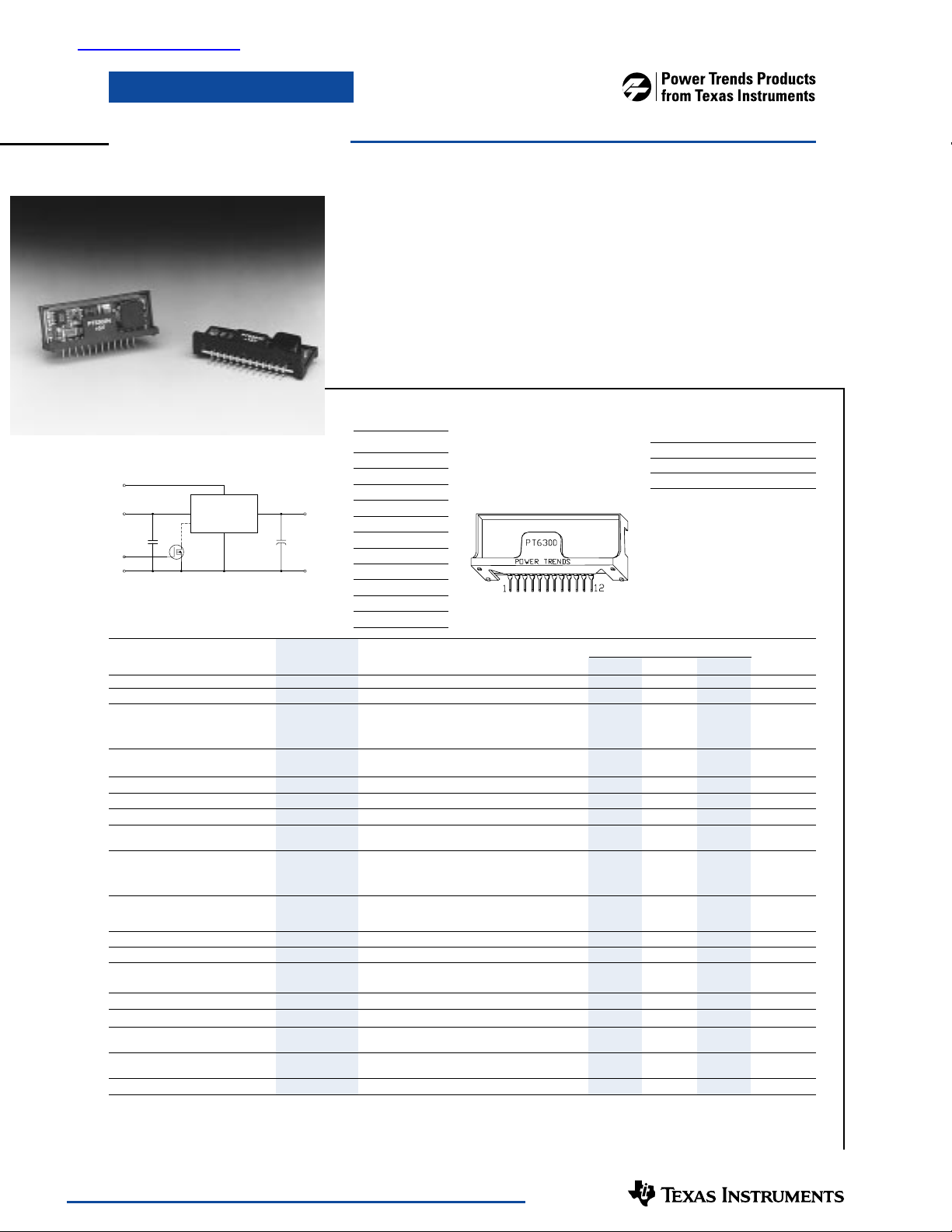
PT6300 Series
3 Amp Adjustable Positive S tep-down
Integrated S w itching Regulators
SLTS031B
(Revised 9/30/2000)
• 90% Efficiency
• Adjustable Output Voltage
• Internal Short Circuit Protection
• Over-Temperature Protection
• On/Off Control (Ground Off)
• Small SIP Footprint
• Wide Input Range
Switching Regulators (ISRs) designed
to meet the on-board power conversion
needs of battery powered or other
equipment requiring high efficiency and
small size. This high performance ISR
family offers a unique combination of
features combining 90% typical efficiency with open-collector on/off
The PT6300 Series is a line of
High-Performance 3 Amp, 12-Pin SIP
(Single In-line Package) Integrated
Pin-Out Information
Pin Function
Inhibit
1
(30V max)
2V
Standard Application
VOADJ
V
IN
C1
INH
COM COM
C1 = Optional 1µF ceramic
= Required 100µF electrolytic
C
2
Q1 = NFET
12
V
2,3,4
PT6300
1
5,6,7,8
Q1
9,10,11
OUT
+
C2
(1)
Specifications
Characteristics
(Ta=25°C unless noted) Symbols Conditions Min Typ Max Units
Output Current I
Short Circuit Current I
Input Voltage Range V
(Note: inhibit function cannot Vo = 5.0V 9 — 30/38
be used above 30V.) V
Output Voltage Tolerance ∆V
Line Regulation Reg
Load Regulation Reg
Vo Ripple/Noise V
Transient Response t
with Co = 100µF V
Efficiency η V
Switching Frequency ƒ
Shutdown Current I
Quiescent Current I
Absolute Maximum T
Operating Temperature Range
Thermal Resistance θ
Storage Temperature T
Mechanical Shock Per Mil-STD-883D, Method 2002.3, 1 msec,
Mechanical Vibration Per Mil-STD-883D, Method 2007.2,
Weight — — — 6.5 — grams
Notes:
(1) The PT6300 Series requires a 100µF electrolytic or tantalum output capacitor for proper operation in all applications.
(2) The ISR will operate to no load with reduced specifications.
(3) Input voltage cannot exceed 30V when the inhibit function is used.
(4) See Thermal Derating charts.
(5) Consult the related application note for guidance on adjusting the output voltage.
o
sc
in
o
line
load
n
tr
os
o
sc
nl
a
ja
s
in
3V
in
4V
in
5 GND
6 GND
7 GND
8 GND
9V
out
10 V
out
11 V
out
out
Adj
(5)
12 V
Over Vin range 0.1
Vin = Vo + 5V — 5.0 — Apk
0.1 ≤ Io ≤ 3.0 A V
Over Vin Range, Io = 3.0 A
Ta = 0°C to +60°C
Over Vin range — ±0.25 ±0.5 %V
0.1 ≤ Io ≤ 3.0 A — ±0.25 ±0.5 %V
V
= V
min, Io = 3.0 A — ±2 — %V
in
in
50% load change — 100 200 µSec
Vo over/undershoot — 5.0 — %V
=16V, Io = 0.5 A, Vo = 12V — 91 —
in
V
=9V, Io = 0.5 A, Vo = 5.0V — 89 —
in
V
=9V, Io = 0.5 A, Vo = 3.3V — 84 —
in
Vin=9V, Io =0.5A, Vo = 1.5V — 72 —
Over Vin and Io ranges, Vo = 12V 600 750 900
Vin = 15V — 100 — µA
Io = 0A, V
=10V — 10 — mA
in
Over Vin range -40 — +85
Free Air Convection (40-60LFM) — 30 — °C/W
— -40 — +125 °C
Half Sine, mounted to a fixture
20-2000 Hz,Soldered in a PC board
Ordering Information
PT6302
¨ = +5 Volts
PT6303
¨ = +3.3 Volts
PT6304
¨ = +12 Volts
PT6314
¨ = +1.5Volts
Pkg Style 200
= 12V 16 — 30/38
o
= 3.3V 9 — 26
o
Vo = 1.5V 9.0 — 17
V
= 3.3V/5V 400 500 600 kHz
o
Vo = 1.5V 350 450 550
control and adjustable output voltage.
Quiescent current in the shutdown
mode is typically less than 100µA.
PT Series Suffix
Case/Pin
Configuration
Vertical Through-Hole
Horizontal Through-Hole
Horizontal Surface Mount
PT6300 SERIES
(2)
— 3.0 A
— ±1.0 ±2.0 %V
— 500
— 10 — G’s
—
(PT1234X)
(3)
(3)
(4)
N
A
C
V
o
o
o
o
o
%
°C
G’s
For technical support and more information, see inside back cover or visit www.ti.com/powertrends
Page 2
V
PT6300 Series
3 Amp Adjustable Positive Step-down
Integrated S w itching Regulators
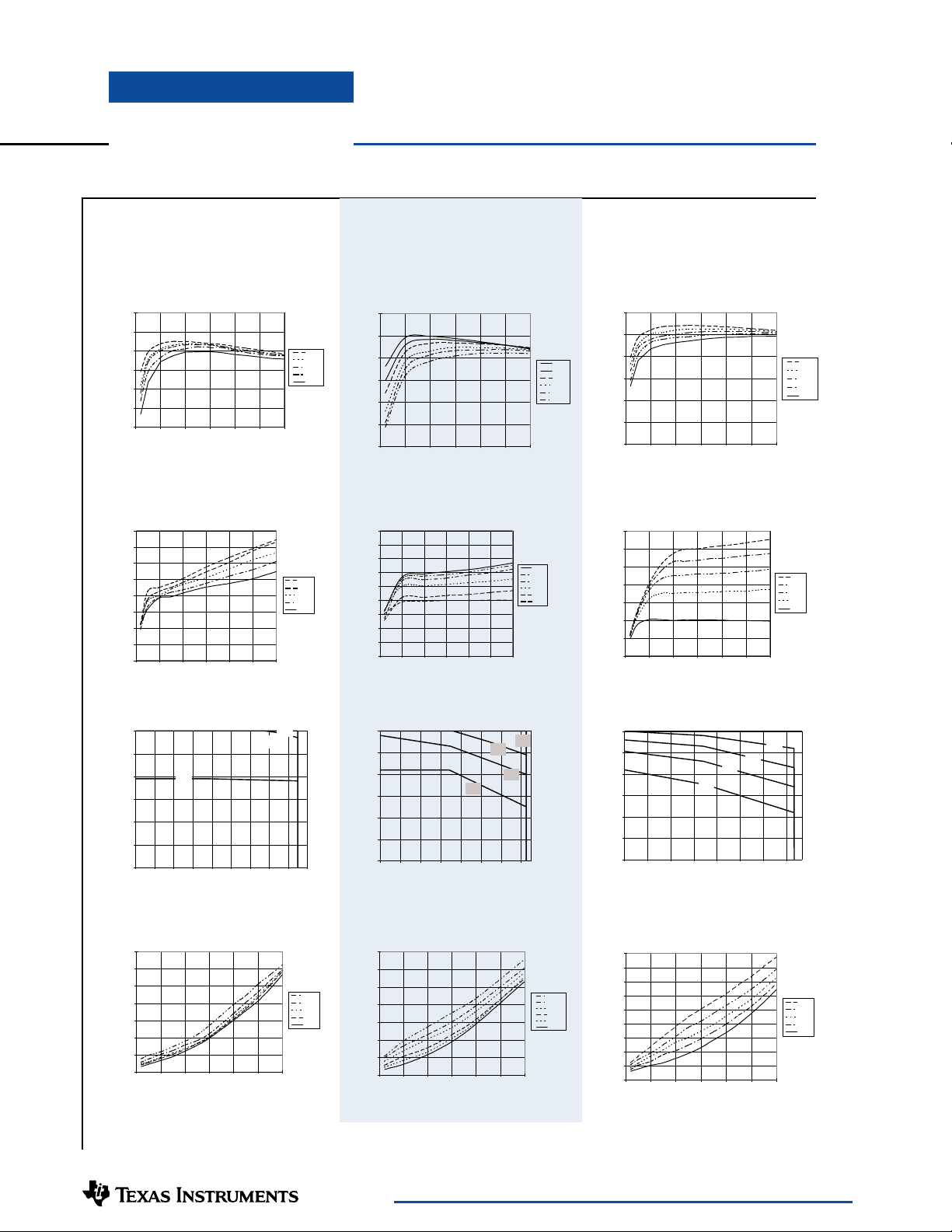
Typical Characteristics
PT6303, 3.3 VDC
Efficiency vs Output Current
100
90
80
70
60
Efficiency - %Ripple-(mV)Iout-(Amps)PD-(Watts)
50
40
00.511.522.53
Iout-(Amps)
(See Note A)
PT6302, 5.0 VDC
Efficiency vs Output Current Efficiency vs Output Current
100
Vin
9.0V
12.0V
15.0V
20.0V
26.0V
90
80
70
Efficiency - %
60
50
40
00.511.522.53
Iout-(Amps)
Ripple vs Output Current Ripple vs Output Current
160
140
120
100
80
60
40
20
0
00.51 1.522.53
Iout-(Amps)
Vin
26.0V
20.0V
15.0V
12.0V
9.0V
180
160
140
120
100
80
Ripple-(mV)
60
40
20
0
00.511.522.53
Iout-(Amps)
(See Note A)
Vin
38.0V
30.0V
24.0V
15.0V
12.0V
9.0V
PT6304, 12.0 VDC
100
90
Vin
9.0V
12.0V
15.0V
24.0V
30.0V
38.0V
80
70
Efficiency - %
60
50
40
0 0.5 1 1.5 2 2.5 3
(See Note A)
Vin
16.0V
20.0V
24.0V
30.0V
38.0V
Iout-(Amps)
Ripple vs Output Current
350
300
250
200
150
100
Ripple-(mV)Iout-(Amps)
50
0
00.511.522.53
Iout-(Amps)
Vin
38.0V
30.0V
24.0V
20.0V
16.0V
)
Thermal Derating (T
3
2.5
2
1.5
1
0.5
0
85°C
9 111315171921232527
a
(See Note B)
60°C
70°C
Thermal Derating (Ta)
3
2.5
2
1.5
1
Iout-(Amps)
0.5
0
9 13172125293337
85°C
(See Note B)
50°C
60°C
70°C
Thermal Derating (Ta)
3
2.5
2
1.5
1
0.5
0
16 19 22 25 28 31 34 37
Vin-(Volts) Vin-(Volts)Vin-(Volts)
Power Dissipation vs Output Current Power Dissipation vs Output Current
3.5
3
2.5
2
1.5
1
0.5
0
0 0.5 1 1.5 2 2.5 3
Vin
26.0V
20.0V
15.0V
12.0V
9.0V
3.5
3
2.5
2
1.5
PD-(Watts)
1
0.5
0
0 0.5 1 1.5 2 2.5 3
Vin
38.0V
30.0V
24.0V
15.0V
12.0V
9.0V
Power Dissipation vs Output Current
4.5
4
3.5
3
2.5
2
PD-(Watts)
1.5
1
0.5
0
00.511.522.53
Iout-(Amps) Iout-(Amps) Iout-(Amps)
Note A:
Characteristic data listed in the above graphs has been developed from actual products tested at 25°C. This data is considered typical data for the ISR
Note B:
Thermal derating graphs are developed in free air convection cooling of 40-60 LFM. (See Thermal Application note.)
70°C
60°C
(See Note B)
40°C
50°C
Vin
38.0V
30.0V
24.0V
20.0V
16.0V
For technical support and more information, see inside back cover or visit www.ti.com/powertrends
Page 3
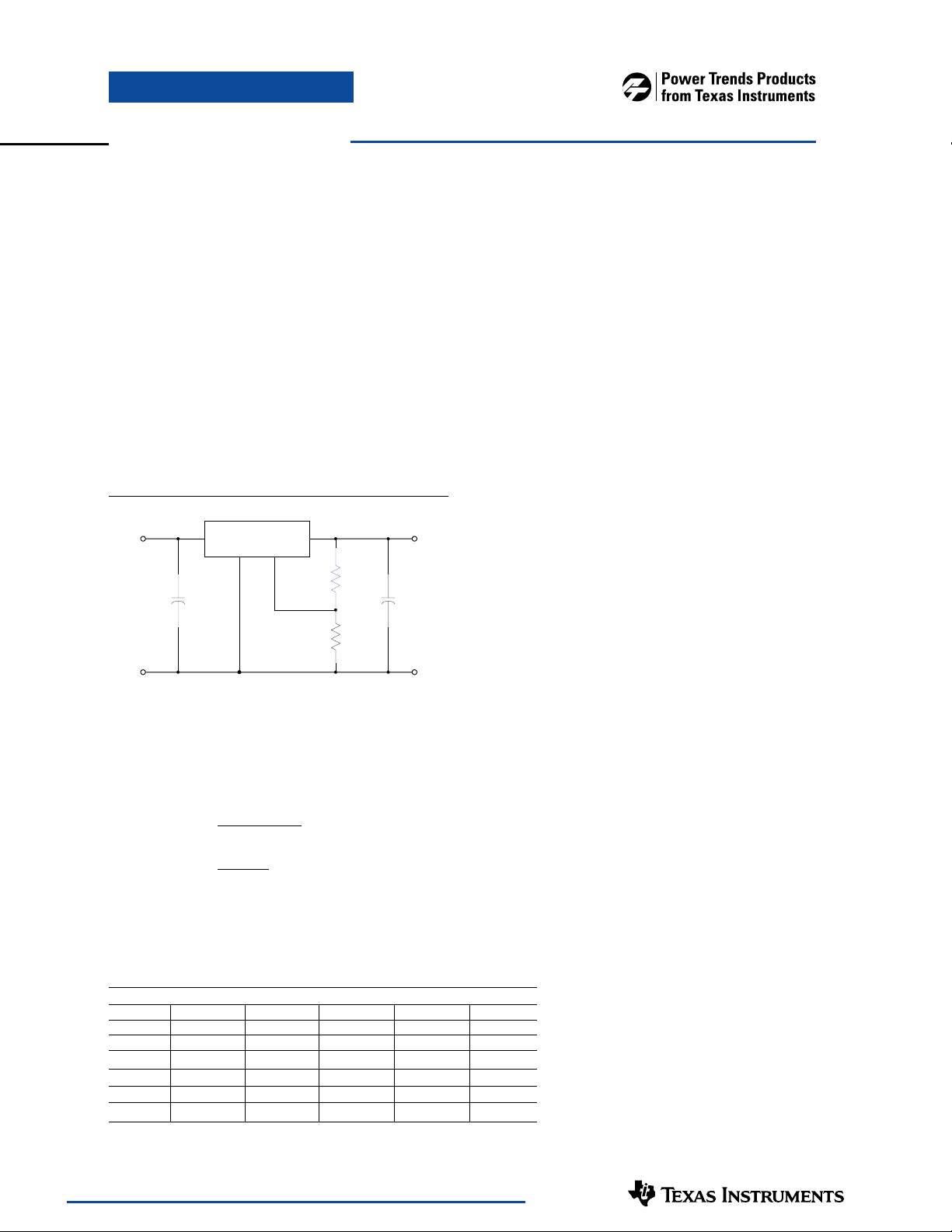
Application Notes
PT6100/6210/6300 Series
Adjusting the Output Vo ltage of Power Trends’
Wide Input Range Bus ISRs
The output voltage of the Power Trends’ Wide Input
Range Series ISRs may be adjusted higher or lower than
the factory trimmed pre-set voltage with the addition of a
single external resistor. Table 1 accordingly gives the
allowable adjustment range for each model for either
series as V
Adjust Up:
adding a resistor R2, between pin 12 (V
(GND).
Adjust Down:
and pins 9-11(V
Figure 1
Vin
C1
F Ceramic
1
µ
(Optional)
(min) and Va (max).
a
An increase in the output voltage is obtained by
adjust) and pins 5-8
o
Add a resistor (R1), between pin 12 (Vo adjust)
).
out
PT6100/6200/6300
2,3,4
Vin Vo
GND Vo(adj)
125,6,7,8
(R1)
Adj Down
R2
Adjust
Up
9,10,11
C2
F
100
µ
(Req'd)
+
Vo
COMCOM
Notes:
1. Use only a single 1% resistor in either the (R1) or R2
location. Place the resistor as close to the ISR as possible.
2. Never connect capacitors from V
. Any capacitance added to the Vo adjust pin will
or V
out
adjust to either GND
o
affect the stability of the ISR.
3. Adjustments to the output voltage may place additional
limits on the maximum and minimum input voltage for
the part. The revised maximum and minimum input
voltage limits must comply with the following
requirements. The limits are model dependant.
PT6216/PT6314:
Vin (max) = (10 x Va)V or 17V, whichever is less.
(min) = 9.0V
V
in
All other models:
Vin (max) = (8 x Va)V or as specified.
Vin (min) = (Va + 4)V or 9V, whichever is greater.
The values of (R1) [adjust down], and R2 [adjust up], can
also be calculated using the following formulas. Refer to
Figure 1 and Table 2 for both the placement and value of the
required resistor; either (R1) or R2 as appropriate.
(R1) =
R2 =
Ro (Va – 1.25)
V
– V
o
a
1.25 R
o
– V
V
a
o
kΩ
kΩ
Where: Vo= Original output voltage
= Adjusted output voltage
V
a
= The resistance value fromTable 1
R
o
Table 1
ISR ADJUSTMENT RANGE AND FORMULA PARAMETERS
1Adc Rated PT6102 PT6101 PT6103
2Adc Rated PT6216 PT6213 PT6212 PT6214
3Adc Rated PT6314 PT6303 PT6302 PT6304
Vo (nom)
Va (min)
Va (max)
ΩΩ
Ω
Ro (k
ΩΩ
1.5 3.3 5.0 5.0 12.0
1.3 1.8 1.88 2.18 2.43
1.9 6.07 11.25 8.5 22.12
)
8.25 66.5 150.0 90.9 243.0
For technical support and more information, see inside back cover or visit www.ti.com/powertrends
Page 4

Application Notes
continued
PT6100/6210/6300 Series
Table 2
ISR ADJUSTMENT RESISTOR VALUES
1Adc Rated PT6102 PT6101 PT6103
2Adc Rated PT6216 PT6213 PT6212 PT6214
3Adc Rated PT6314 PT6303 PT6302 PT6304
Vo (nom) 1.5 3.3 5.0 5.0 12.0
Va (req.d)
1.3 (2.1kΩ)
1.4 (12.4kΩ)
1.5
1.6 103.0kΩ
1.7 51.6kΩ
1.8 34.4kΩ (24.4)kΩ
1.9 25.8kΩ (30.9)kΩ (31.5)kΩ
2.0 (38.4)kΩ (37.5)kΩ
2.1 (47.1)kΩ (44.0)kΩ
2.2 (57.4)kΩ (50.9)kΩ (30.8)kΩ
2.3 (69.8)kΩ (58.3)kΩ (35.4)kΩ
2.4 (85.0)kΩ (66.3)kΩ (40.2)kΩ
2.5 (104.0)kΩ (75.0)kΩ (45.5)kΩ (32.0)kΩ
2.6 (128.0)kΩ (84.4)kΩ (51.1)kΩ (34.9)kΩ
2.7 (161.0)kΩ (94.6)kΩ (57.3)kΩ (37.9)kΩ
2.8 (206.0)kΩ (106.0)kΩ (64.0)kΩ (40.9)kΩ
2.9 (274.0kΩ (118.0)kΩ (71.4)kΩ (44.1)kΩ
3.0 (388.0)kΩ (131.0)kΩ (79.5)kΩ (47.3)kΩ
3.1 (615.0)kΩ (146.0)kΩ (88.5)kΩ (50.5)kΩ
3.2 (1300.0)kΩ (163.0)kΩ (98.5)kΩ (53.8)kΩ
3.3 (181.0)kΩ (110.0)kΩ (57.3)kΩ
3.4 831.0kΩ (202.0)kΩ (122.0)kΩ (60.8)kΩ
3.5 416.0kΩ (225.0)kΩ (136.0)kΩ (64.3)kΩ
3.6 227.0kΩ (252.0)kΩ (153.0)kΩ (68.0)kΩ
3.7 208.0kΩ (283.0)kΩ (171.0)kΩ (71.7)kΩ
3.8 166.0kΩ (319.0)kΩ (193.0)kΩ (75.6)kΩ
3.9 139.0kΩ (361.0)kΩ (219.0)kΩ (79.5)kΩ
4.0 119.0kΩ (413.0)kΩ (250.0)kΩ (83.5)kΩ
4.1 104.0kΩ (475.0)kΩ (288.0)kΩ (87.7)kΩ
4.2 92.4kΩ (533.0)kΩ (335.0)kΩ (91.9)kΩ
4.3 83.1kΩ (654.0)kΩ (396.0)kΩ (96.3)kΩ
4.4 75.6kΩ (788.0)kΩ (477.0)kΩ (101.0)kΩ
4.5 69.3kΩ (975.0)kΩ (591.0)kΩ (105.0)kΩ
4.6 63.9kΩ (1260.0)kΩ (761.0)kΩ (110.0)kΩ
4.7 59.4kΩ (1730.0)kΩ (1050.0)kΩ (115.0)kΩ
4.8 55.4kΩ (1610.0)kΩ (120.0)kΩ
4.9 52.0kΩ (125.0)kΩ
5.0 48.9kΩ (130.0)kΩ
5.1 46.2kΩ 1880.0kΩ 1140.0kΩ (136.0)kΩ
5.2 43.8kΩ 937.0kΩ 568.0kΩ (141.0)kΩ
5.3 41.6kΩ 625.0kΩ 379.0kΩ (147.0)kΩ
5.4 39.6kΩ 469.0kΩ 284.0kΩ (153.0)kΩ
5.5 37.8kΩ 375.0kΩ 227.0kΩ (159.0)kΩ
5.6 36.1kΩ 313.0kΩ 189.0kΩ (165.0)kΩ
5.7 34.6kΩ 268.0kΩ 162.0kΩ (172.0)kΩ
5.8 33.3kΩ 234.0kΩ 142.0kΩ (178.0)kΩ
5.9 32.0kΩ 208.0kΩ 126.0kΩ (185.0)kΩ
6.0 30.8kΩ 188.0kΩ 114.0kΩ (192.0)kΩ
ISR ADJUSTMENT RESISTOR VALUES (Cont)
1Adc Rated PT6101 PT6103
2Adc Rated PT6212 PT6214
3Adc Rated PT6302 PT6304
Vo (nom) 5.0 5.0 12.0
Va (req.d)
6.2 156.0kΩ 94.7kΩ (207.0)kΩ
6.4 134.0kΩ 81.2kΩ (223.0)kΩ
6.6 117.0kΩ 71.0kΩ (241.0)kΩ
6.8 104.0kΩ 63.1kΩ (259.0)kΩ
7.0 93.8kΩ 56.8kΩ (279.0)kΩ
7.2 85.2kΩ 51.6kΩ (301.0)kΩ
7.4 78.1kΩ 47.3kΩ (325.0)kΩ
7.6 72.1kΩ 43.7kΩ (351.0)kΩ
7.8 67.0kΩ 40.6kΩ (379.0)kΩ
8.0 62.5kΩ 37.9kΩ (410.0)kΩ
8.2 58.6kΩ 35.5kΩ (444.0)kΩ
8.4 55.1kΩ 33.4kΩ (483.0)kΩ
8.6 52.1kΩ (525.0)kΩ
8.8 49.3kΩ (573.0)kΩ
9.0 46.9kΩ (628.0)kΩ
9.5 41.7kΩ (802.0)kΩ
10.0 37.5kΩ (1060.0)kΩ
10.5 34.1kΩ (1500.0)kΩ
11.0 31.3kΩ
11.5
12.0
12.5 608.0kΩ
13.0 304.0kΩ
13.5 203.0kΩ
14.0 152.0kΩ
14.5 122.0kΩ
15.0 101.0kΩ
15.5 86.8kΩ
16.0 75.9kΩ
16.5 67.5kΩ
17.0 60.8kΩ
17.5 55.2kΩ
18.0 50.6kΩ
18.5 46.7kΩ
19.0 43.4kΩ
19.5 40.5kΩ
20.0 38.0kΩ
20.5 35.7kΩ
21.5 33.8kΩ
21.5 32.0kΩ
22.0 30.4kΩ
R1 = (Blue) R2 = Black
For technical support and more information, see inside back cover or visit www.ti.com/powertrends
Page 5

Application Notes
PT6100/6210/6300 Series
Using the Inhibit Function on Power Trends’
Wide Input Range Bus ISRs
For applications requiring output voltage On/Off control,
the 12pin ISR products incorporate an inhibit function.
The function has uses in areas such as battery conservation,
power-up sequencing, or any other application where the
regulated output from the module is required to be
switched off. The On/Off function is provided by the
Pin 1 (Inhibit) control.
The ISR functions normally with Pin 1 open-circuit,
providing a regulated output whenever a valid source
voltage is applied to V
level2 ground signal is applied to Pin 1, the regulator
, (pins 2, 3, & 4). When a low-
in
output will be disabled.
Figure 1 shows an application schematic, which details
the typical use of the Inhibit function. Note the discrete
transistor (Q1). The Inhibit control has its own internal
pull-up with a maximum open-circuit voltage of 8.3VDC.
Only devices with a true open-collector or open-drain
output can be used to control this pin. A discrete bipolar
transistor or MOSFET is recommended.
Equation 1 may be used to determine the approximate
current drawn by Q1 when the inhibit is active.
Equation 1
I
stby
=V
÷ 155kΩ ± 20%
in
Figure 1
V
in
C1, 1µF
(Optional)
Inh
COM
Turn-On Time:
PT6100/6210/6300
2,3,4
Vin Vo
GND Vo(adj)
Inh*
1
Q1
BSS138
The output of the ISR is enabled automatically
9,10,11
125,6,7,8
C2
µ
100
F
V
out
+
COM
when external power is applied to the input. The Inhibit control
pin is pulled high by its internal pull-up resistor. The ISR
produces a fully regulated output voltage within 1-msec of
either the release of the Inhibit control pin, or the application
of power. The actual turn-on time will vary with the input
voltage, output load, and the total amount of capacitance connected to the output Using the circuit of Figure 1, Figure 2
shows the typical rise in output voltage for the PT6101
following the turn-off of Q1 at time t =0. The waveform was
measured with a 9Vdc input voltage, and 5-Ohm resistive load.
Figure 2
Notes:
1. The Inhibit control logic is similar for all Power Trends’
modules, but the flexibility and threshold tolerances will be
different. For specific information on the inhibit function
of other ISR models, consult the applicable application
note.
2. Use only a true open-collector device (preferably a discrete
transistor) for the Inhibit input.
Do Not use a pull-up
resistor, or drive the input directly from the output of a
TTL or other logic gate. To disable the output voltage,
the control pin should be pulled low to less than +1.5VDC.
3. When the Inhibit control pin is active, i.e. pulled low, the
maximum allowed input voltage is limited to +30Vdc.
4. Do not control the Inhibit input with an external DC
voltage. This will lead to erratic operation of the ISR and
may over-stress the regulator.
5. Avoid capacitance greater than 500pF at the Inhibit control
pin. Excessive capacitance at this pin will cause the ISR to
produce a pulse on the output voltage bus at turn-on.
6. Keep the On/Off transition to less than 10µs. This
prevents erratic operation of the ISR, which can cause a
momentary high output voltage.
6
5
4
3
(Vdc)
o
V
2
1
0
-0.2 0 0.2 0.4 0.6 0.8 1
t (mill i -secs)
For technical support and more information, see inside back cover or visit www.ti.com/powertrends
Page 6

IMPORTANT NOTICE
T exas Instruments and its subsidiaries (TI) reserve the right to make changes to their products or to discontinue
any product or service without notice, and advise customers to obtain the latest version of relevant information
to verify, before placing orders, that information being relied on is current and complete. All products are sold
subject to the terms and conditions of sale supplied at the time of order acknowledgment, including those
pertaining to warranty, patent infringement, and limitation of liability.
TI warrants performance of its semiconductor products to the specifications applicable at the time of sale in
accordance with TI’s standard warranty. Testing and other quality control techniques are utilized to the extent
TI deems necessary to support this warranty . Specific testing of all parameters of each device is not necessarily
performed, except those mandated by government requirements.
Customers are responsible for their applications using TI components.
In order to minimize risks associated with the customer’s applications, adequate design and operating
safeguards must be provided by the customer to minimize inherent or procedural hazards.
TI assumes no liability for applications assistance or customer product design. TI does not warrant or represent
that any license, either express or implied, is granted under any patent right, copyright, mask work right, or other
intellectual property right of TI covering or relating to any combination, machine, or process in which such
semiconductor products or services might be or are used. TI’s publication of information regarding any third
party’s products or services does not constitute TI’s approval, warranty or endorsement thereof.
Copyright 2000, Texas Instruments Incorporated
Page 7

Copyright © Each Manufacturing Company.
All Datasheets cannot be modified without permission.
This datasheet has been download from :
www.AllDataSheet.com
100% Free DataSheet Search Site.
Free Download.
No Register.
Fast Search System.
www.AllDataSheet.com
 Loading...