

PT3320
30 WATT ISOLATED
DC/DC CONVERTER
Power Trends, Inc. 27715 Diehl Road, Warrenville, IL 60555 (800) 531-5782 Fax: (630) 393-6902 http://www.powertrends.com
Series
For assistance or to order, call (800) 531-5782
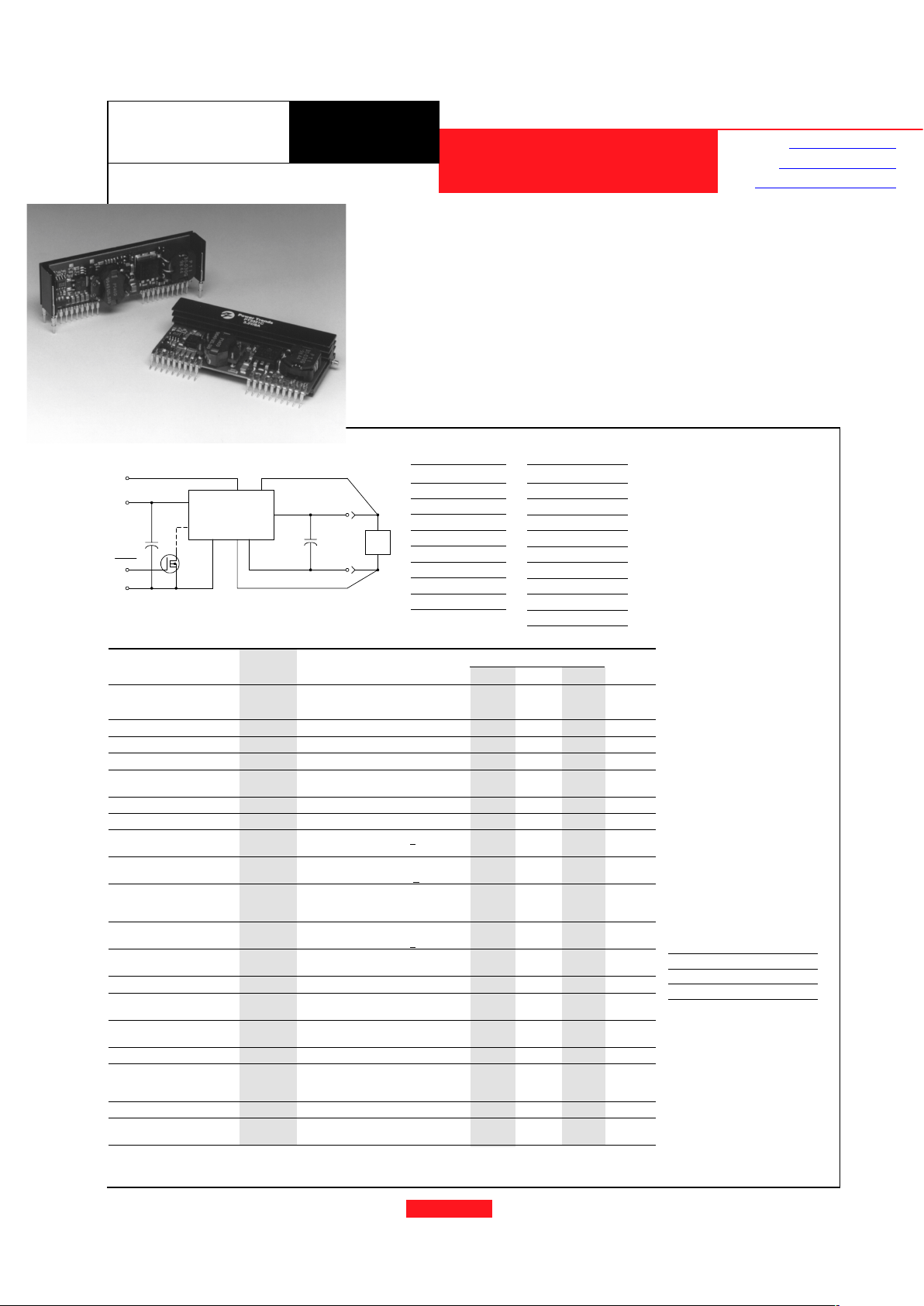
Standard Application
Cin= Optional 100µF/100V electrolytic
C
out
= Required 330µF electrolytic
Q1= NFET
PT3320
7-9
4-6
14-17
+V
IN
-V
IN
+V
O
C
OUT
+
C
IN
+
19
+REMOTE SENSE
10-12
2
LOAD
18
-V
O
13
Q
1
-REMOTE SENSE
Inhibit
VO Adjust
• 30W Output Power
• Input Voltage Range:
36V to 75V
• 1500 VDC Isolation
• Vo Inhibit
• V
o
Adjust
• Differential Remote Sense
• Current Limit
• Short-Circuit Protection
• Over-Temperature Shutdown
• Undervoltage Lockout
• Flexibile SIP Package
• UL 1950, CSA 22.2 950
approval pending
• Meets EN60950
Features
The PT3320 is a new series of highinput voltage, 30 Watt, isolated DC to
DC converters housed in a unique
vertical or horizontal 19-pin SIP package. The 36 to 75V input range allows
easy integration into many distributed
power applications which utilize 48V bus
architectures.
The PT3320 series is available with
output voltages from 2V to 15V. The
output voltage is adjustable from 90 to
110% of nominal with the addition of an
external resistor. Other easy to use
features include an inhibit function and
differential remote sense which automatically compensates for any voltage
drop from the converter to the load. The
PT3320 includes built in current limit,
short circuit protection and overtemperature shutdown.
The PT3320 requires a 330µF output
capacitor for proper operation.
(For dimensions and PC board layout,
see Package Styles 840 and 850.)
PT Series Suffix
(PT1234X)
Case/Pin
Configuration
Vertical Through-Hole
N
Horizontal Through-Hole
A
Horizontal Surface Mount
C
Ordering Information
PT3321¨ = 3.3V/8A
PT3322¨ = 5.0V/6A
PT3323¨ = 12.0V/2.5A
PT3324¨ = 15.0V/2A
PT3325¨ = 2.0V/8A
PT3326¨ = 2.5V/8A
PT3327¨ = 1.8V/8A
PT3328¨ = 5.2V/6A
Preliminary Specifications
Characteristics
PT3320 SERIES
(Ta = 25°C unless noted) Symbols Conditions Min Typ Max Units
Output Current I
o
Over Vin range Vo = 3.3V 0.25 — 8.0 A
V
o
= 5V 0.25 — 6.0 A
Vo = 12V 0.1 — 2.5 A
On/Off Standby Current I
in standby
Vin = 48V, Pin 1 = -V
in
—8 16mA
Short Circuit Current I
sc
Vin = 48V — 2xI
omax
—A
Input Voltage Range V
in
Over Io Range 36.0 48.0 75.0 V
Output Voltage Tolerance ∆V
o
Over Vin Range
TA= -40°C to +85°C
— ±1.0 — %V
o
Line Regulation Reg
line
Over Vin range @ max I
o
— ±0.5 — %V
o
Load Regulation Reg
load
10% to 100% of Io max — ±0.5 — %V
o
Vo Ripple/Noise V
n
Vin=48V, Io=Io max, Vo>5V — 1.0 — %V
o
Vin=48V, Io=Io max, Vo<5V — 50 — mV
pp
Transient Response t
tr
50% load change, 1A/µSec — 100 — µSec
Vo over/undershoot, Vo>5V — 3.0 — %V
o
Efficiency η Vin=48V, Io=6A, Vo=3.3V — 80 — %
V
in
=48V, Io=6A, Vo=5V — 84 — %
Vin=48V, Io=2.5A, Vo=12V — 85 — %
Switching Frequency ƒ
o
Over Vin and Io Vo<10V 600 750 900 kHz
Vo>10V 400 500 600 kHz
Recommended Operating T
a
Vin = 48V @ max I
o
-40* — +85 °C
Temperature Range Airflow = 200 LFM
Storage Temperature T
s
— -40 — +125 °C
Mechanical Shock — Per Mil-Std-883D, method 2002.3,
— 500 — G’s
1mS, half-sine, mounted to a fixture
Mechanical Vibration — Per Mil-Std-883D, method 2007.2,
—10—G’s
20-2000Hz, soldered in a PC board
Weight — — — 40 — grams
Input/Output Isolation — — 1500 — — VDC
Capacitance — — — 1200 — pF
Resistance — — 10 — — MΩ
Flammability — Materials meet UL 94V-0
Inhibit (pin 2) On**
Referenced to -V
in
2.5 — 15 VDC
Off 0 — 0.8 VDC
* At temperatures below 0°C, the PT3320 series requires output capacitors with temperature stable dielectrics
such as tantalum or Oscon.
** If pin 2 is left open, the PT3320 will operate when input power is applied.
Pin-Out Information
Pin Function
1 Do Not Use
2 Inhibit
3 Do Not Use
4-V
in
5-V
in
6-V
in
7+V
in
8+V
in
9+V
in
Pin Function
10 -V
o
11 -V
o
12 -V
o
13 -Remote Sense
14 +V
o
15 +V
o
16 +V
o
17 +V
o
18 Vo Adjust
19 +Remote Sense
* Note: This product is the
subject of one or more patents.
Other patents pending.
Patent pending*
New 30W Isolated SIPs
Revised 5/19/99
Application Notes
Mechanical Outline
Product Selector Guide
For assistance or to order, call (800) 531-5782
Power Trends, Inc. 27715 Diehl Road, Warrenville, IL 60555 (800) 531-5782 Fax: (630) 393-6902 http://www.powertrends.com
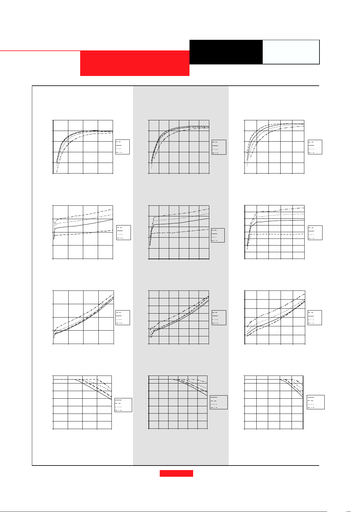
Note 1: All data listed in the above graphs has been developed from actual products tested at 25°C. This data is considered typical data for the DC-DC Converter.
PT3322, 5.0 VDC (See Note 1) PT3323, 12.0 VDC (See Note 1)
Efficiency vs Output Current Efficiency vs Output Current Efficiency vs Output Current
Ripple vs Output Current Ripple vs Output Current Ripple vs Output Current
Power Dissipation vs Output Current Power Dissipation vs Output Current Power Dissipation vs Output Current
PT3321, 3.3 VDC (See Note 1)
Efficiency (%)Ripple (mV)PD (Watts)
Efficiency (%)
Efficiency (%)
Ripple (mV)
Ripple (mV)PD (Watts)
PD (Watts)
Iout (A) Iout (A)
Iout (A) Iout (A) Iout (A)
Iout (A) Iout (A)Iout (A)
Iout (A)
SeriesPT3320
CHARACTERISTIC DATA
40
50
60
70
80
90
02468
36.0V
48.0V
60.0V
75.0V
40
50
60
70
80
90
0123456
36.0V
48.0V
60.0V
75.0V
40
50
60
70
80
90
0.0 0.5 1.0 1.5 2.0 2.5
36.0V
48.0V
60.0V
75.0V
Vin
Vin
Vin
0
10
20
30
40
02468
36.0V
48.0V
60.0V
75.0V
0
2
4
6
8
02468
36.0V
48.0V
60.0V
75.0V
Vin
Vin
0
10
20
30
40
50
012345 6
36.0V
48.0V
60.0V
75.0V
Vin
0
1
2
3
4
5
6
7
0123456
36.0V
48.0V
60.0V
75.0V
Vin
0
20
40
60
80
100
120
140
160
0.0 0.5 1.0 1. 5 2.0 2.5
36.0V
48.0V
60.0V
75.0V
Vin
0
1
2
3
4
5
6
0.0 0. 5 1.0 1.5 2.0 2.5
36.0V
48.0V
60.0V
75.0V
Vin
Safe Operating Area (@Vin=48V) Safe Operating Area (@Vin=48V) Safe Operating Area (@Vin=48V)
Iout (A) Iout (A) Iout (A)
20
30
40
50
60
70
80
90
02468
Nat conv
60LFM
120LFM
200LFM
Ambient Temperature (°C)
20
30
40
50
60
70
80
90
0123456
Nat conv
60LFM
120LFM
200LFM
20
30
40
50
60
70
80
90
0 0.5 1 1.5 2 2.5
Nat conv
60LFM
120LFM
200LFM
Ambient Temperature (°C)
Ambient Temperature (°C)
Airflow
Airflow
Airflow

For assistance or to order, call (800) 531-5782
3
Power Trends, Inc. 27715 Diehl Road, Warrenville, IL 60555 (800) 531-5782 Fax: (630) 393-6902 http://www.powertrends.com
Application Notes
PT3320/3340 Series
More Application Notes
Adjusting the Output Voltage of the PT3320 /
PT3340 Series of Isolated DC-DC Converters
The factory pre-set output voltage of Power Trends’ PT3320
and PT3340 series DC-DC converters may be adjusted within a
nominal ±10% range. This is accomplished with the addition of
a single external resistor. For the input voltage range specified in
the data sheet, Table 1 gives the allowable adjustment range for
each model as V
o
(min) and Vo (max).
Adjust Up: An increase in the output voltage is obtained by
adding a resistor, R2 between pin 18 (V
o
adjust), and pin 13
(-Remote Sense).
See note 4.
Adjust Down: Add a resistor (R1), between pin 18 (V
o
adjust)
and pin 19 (+Remote Sense).
Refer to Figure 1 and Table 2 for both the placement and value
of the required resistor, (R1) or R2.
Notes:
1. Use only a single 1% resistor in either the (R1) or R2 location. Place the resistor as close to the ISR as possible.
2. Never connect capacitors to Vo adjust. Any capacitance
added to the Vo adjust control pin will affect the stability of
the ISR.
Table 1
DC-DC CONVERTER ADJUSTMENT RANGE AND FORMULA PARAMETERS
Series Pt #
24V Bus PT3341 PT3342 PT3343 PT3344
48V Bus PT3325 PT3326 PT3321 PT3322 PT3323 PT3324
Vo(nom) 2.0V 2.5 3.3 5.0 12.0 15.0
Vo(min) 1.8V 2.25 2.95 4.5 10.8 13.5
Vo(max) 2.2 2.75 3.65 5.5 13.2 16.5
V
r 1.225 1.225 1.225 1.225 2.5 2.5
Ro (k
ΩΩ
ΩΩ
Ω) 80.6 33.2 33.2 18.2 14.3 11.0
Rs (k
ΩΩ
ΩΩ
Ω) 150.0 121.0 150.0 121.0 90.9 80.6
Figure 1
(R1)
Adj Down
R2
Adj Up
Cin
100
µ
F
100V
(Optional)
+
Cout
330
µ
F
+
L
O
A
D
+V
-V
+V
in
-V
in
PT3320/3340
184, 5, 6
7, 8, 9
+Vin +Vout
-Vin Vo(adj)
Inhibit
2
Sns(+)
19
10 - 12
-Vout
14 - 17
Sns(-)
13
3. If the remote sense pins are not being used, the resistors (R1)
and R2 can be connected to +V
out
or -V
out
respectively.
4. The adjusted output voltage V
a
effectively sets the voltage
across pins 13 and 19 (±Remote Sense). When using the
remote sense pins, V
out
(measured directly across pins 10–12,
and 14–17) can be significantly higher than Va, and may
exceed Vo (max). If Va is adjusted upward, the alternative is
to increase the minimum input voltage by the same percentage as V
out
exceeds Vo(max).
The values of (R1) [adjust down], and R2 [adjust up], can also be
calculated using the following formulas.
(R1) =
R
o
(Vo – Vr)(Va – Vr)
– R
s
kΩ
Vr (Vo – Va)
R2 =
R
o
(Vo – Vr)
– R
s
kΩ
(Va – Vo)
Where V
o
= Original output voltage
V
a
= Adjusted output voltage
V
r
= Reference voltage (Table 1)
R
o
= Multiplier resistance (Table 1)
R
s
= Series resistance (Table 1)

For assistance or to order, call (800) 531-5782
4
Application
Power Trends, Inc. 27715 Diehl Road, Warrenville, IL 60555 (800) 531-5782 Fax: (630) 393-6902 http://www.powertrends.com
Notes
PT3320/3340 Series
Table 2
PT3320 / PT3340 ADJUSTMENT RESISTOR VALUES
Series Pt #
24V Bus PT3341 PT3342 PT3343 PT3344
48V Bus PT3325 PT3326 PT3321 PT3322 PT3323 PT3324
Current 8Adc 8Adc 8Adc 6adc 2.5Adc 2.0Adc
Vo(nom) 2.0Vdc 2.5Vdc 3.3Vdc 5.0Vdc 12.0Vdc 15.0Vdc
Va(req’d) Va(req’d Va(req’d)
1.8 0.0kΩ 4.5 (246.0)kΩ 10.8 (285.0)kΩ
1.85 (62.5)kΩ 4.55 (293.0)kΩ 11.0 (371.0)kΩ
1.9 (194.0)kΩ 4.6 (352.0)kΩ 11.2 (500.0)kΩ
1.95 (589.0)kΩ 4.65 (428.0)kΩ 11.4 (715.0)kΩ
2.0 4.7 (529.0)kΩ 11.6 (1150.0)kΩ
2.05 1100.0kΩ 4.75 (670.0)kΩ 11.8
2.1 475.0kΩ 4.8 (882.0)kΩ 12.0
2.15 266.0kΩ 4.85 (1230.0)kΩ 12.2 588.0kΩ
2.2 162.0kΩ 4.9 (1940.0)kΩ 12.4 249.0kΩ
2.25 (20.7)kΩ 4.95 12.6 136.0kΩ
2.3 (64.7.0)kΩ 5.0 12.8 78.9kΩ
2.35 (138.0)kΩ 5.05 13.0 45.0kΩ
2.4 (285.0)kΩ 5.1 566.0kΩ 13.2 22.3kΩ
2.45 (726.0)kΩ 5.15 337.0kΩ
2.5 5.2 223.0kΩ 13.5 (323.0)kΩ
2.55 726.0kΩ 5.25 154.0kΩ 13.6 (355.0)kΩ
2.6 302.0kΩ 5.3 108.0kΩ 13.8 (437.0)kΩ
2.65 161.0kΩ 5.35 75.3kΩ 14.0 (522.0)kΩ
2.7 90.6kΩ 5.4 50.8kΩ 14.2 (724.0)kΩ
2.75 48.3kΩ 5.45 31.7kΩ 14.4 (1010.0)kΩ
2.95 (127.0)kΩ 5.5 16.4kΩ 14.6 (1580.0)kΩ
3.0 (183.0)kΩ 14.8
3.05 (261.0)kΩ 15.0
3.1 (377.0)kΩ 15.2 607.0kΩ
3.15 (572.0)kΩ 15.4 263.0kΩ
3.2 (961.0)kΩ 15.6 149.0kΩ
3.25 (2130.0)kΩ 15.8 91.3kΩ
3.3 16.0 56.9kΩ
3.35 1230.0kΩ 16.5 11.1kΩ
3.4 539.0kΩ
3.45 309.0kΩ
3.5 194.0kΩ
3.55 126.0kΩ
3.6 79.6kΩ
3.65 46.8kΩ
R1 = (Red) R2 = Black

IMPORTANT NOTICE
T exas Instruments and its subsidiaries (TI) reserve the right to make changes to their products or to discontinue
any product or service without notice, and advise customers to obtain the latest version of relevant information
to verify, before placing orders, that information being relied on is current and complete. All products are sold
subject to the terms and conditions of sale supplied at the time of order acknowledgement, including those
pertaining to warranty, patent infringement, and limitation of liability.
TI warrants performance of its semiconductor products to the specifications applicable at the time of sale in
accordance with TI’s standard warranty. Testing and other quality control techniques are utilized to the extent
TI deems necessary to support this warranty. Specific testing of all parameters of each device is not necessarily
performed, except those mandated by government requirements.
CERT AIN APPLICATIONS USING SEMICONDUCTOR PRODUCTS MAY INVOLVE POTENTIAL RISKS OF
DEATH, PERSONAL INJURY, OR SEVERE PROPERTY OR ENVIRONMENTAL DAMAGE (“CRITICAL
APPLICATIONS”). TI SEMICONDUCTOR PRODUCTS ARE NOT DESIGNED, AUTHORIZED, OR
WARRANTED TO BE SUITABLE FOR USE IN LIFE-SUPPORT DEVICES OR SYSTEMS OR OTHER
CRITICAL APPLICATIONS. INCLUSION OF TI PRODUCTS IN SUCH APPLICA TIONS IS UNDERSTOOD T O
BE FULLY AT THE CUSTOMER’S RISK.
In order to minimize risks associated with the customer’s applications, adequate design and operating
safeguards must be provided by the customer to minimize inherent or procedural hazards.
TI assumes no liability for applications assistance or customer product design. TI does not warrant or represent
that any license, either express or implied, is granted under any patent right, copyright, mask work right, or other
intellectual property right of TI covering or relating to any combination, machine, or process in which such
semiconductor products or services might be or are used. TI’s publication of information regarding any third
party’s products or services does not constitute TI’s approval, warranty or endorsement thereof.
Copyright 1999, Texas Instruments Incorporated
 Loading...