


PGA309-HT
www.ti.com
VOLTAGE OUTPUT PROGRAMMABLE SENSOR CONDITIONER
Check for Samples: PGA309-HT
1
FEATURES
2
• Complete Bridge Sensor Conditioner
• Voltage Output: Ratiometric or Absolute
• Digital Cal: No Potentiometers/Sensor Trims
• Sensor Error Compensation
– Span, Offset, and Temperature Drifts
• Low Error, Time-Stable
• Sensor Linearization Circuitry
• Temperature Sense: Internal or External
• Calibration Lookup Table Logic
– Uses External EEPROM (SOT23-5)
• Over/Under-Scale Limiting
• Sensor Fault Detection
• +2.7V TO +5.5V Operation
• Small TSSOP-16 Package
APPLICATIONS
• Bridge Sensors
• Remote 4-20mA Transmitters
• Strain, Load, and Weigh Scales
• Automotive Sensors
SBOS687A –OCTOBER 2013–REVISED DECEMBER 2013
SUPPORTS EXTREME TEMPERATURE APPLICATIONS
• Controlled Baseline
• One Assembly and Test Site
• One Fabrication Site
• Available in Extreme (–55°C to 150°C)
Temperature Range
(1)
• Extended Product Life Cycle
• Extended Product-Change Notification
• Product Traceability
• Texas Instruments high temperature products
utilize highly optimized silicon (die) solutions
with design and process enhancements to
maximize performance over extended
temperatures. All devices are characterized
and qualified for 1000 hours continuous
operating life at maximum rated temperature.
EVALUATION TOOLS
• Hardware Designer’s Kit (PGA309EVM)
– Temperature Eval of PGA309 + Sensor
– Full Programming of PGA309
– Sensor Compensation Analysis Tool
(1) Custom temperature ranges available
DESCRIPTION
The PGA309 is a programmable analog signal conditioner designed for bridge sensors. The analog signal path
amplifies the sensor signal and provides digital calibration for zero, span, zero drift, span drift, and sensor
linearization errors with applied stress (pressure, strain, etc.). The calibration is done via a One-Wire digital serial
interface or through a Two-Wire industry-standard connection. The calibration parameters are stored in external
nonvolatile memory (typically SOT23-5) to eliminate manual trimming and achieve long-term stability.
The all-analog signal path contains a 2x2 input multiplexer (mux), auto-zero programmable-gain instrumentation
amplifier, linearization circuit, voltage reference, internal oscillator, control logic, and an output amplifier.
Programmable level shifting compensates for sensor dc offsets.
The core of the PGA309 is the precision, low-drift, no 1/f noise Front-End PGA (Programmable Gain Amplifier).
The overall gain of the Front-End PGA + Output Amplifier can be adjusted from 2.7V/V to 1152V/V. The polarity
of the inputs can be switched through the input mux to accommodate sensors with unknown polarity output. The
Fault Monitor circuit detects and signals sensor burnout, overload, and system fault conditions.
1
Please be aware that an important notice concerning availability, standard warranty, and use in critical applications of
Texas Instruments semiconductor products and disclaimers thereto appears at the end of this data sheet.
2All trademarks are the property of their respective owners.
PRODUCTION DATA information is current as of publication date.
Products conform to specifications per the terms of the Texas
Instruments standard warranty. Production processing does not
necessarily include testing of all parameters.
Copyright © 2013, Texas Instruments Incorporated
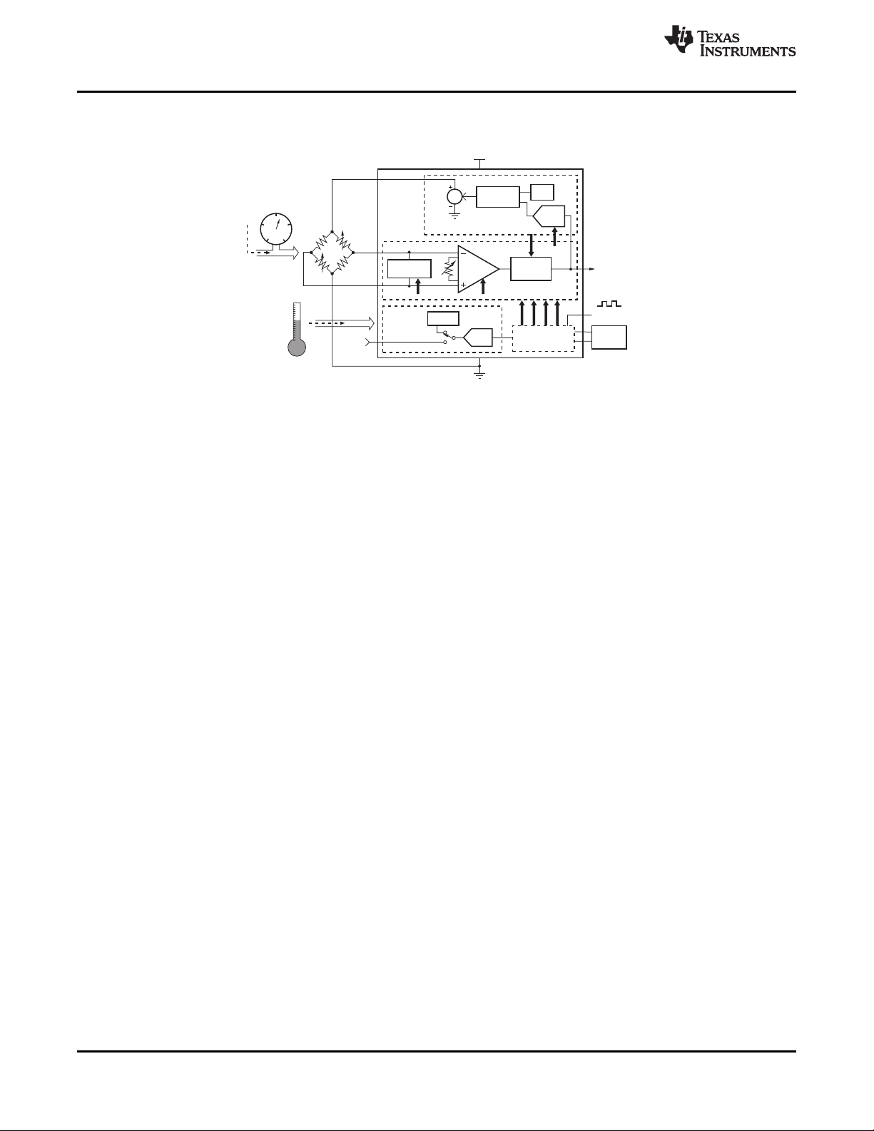
Analog Sensor Linearization
Digital
Temperature
Compensation
Analog Signal Conditioning
PGA309
Digital Cal
VEXC
0
50
psi
P
Ext Temp
Ext Temp
Nonlinear
Bridge
Transducer
Linearization
Circuit
Auto- Zero
PGA
Fault
Monitor
Int Temp
Control Register
Interface Circuitry
EEPROM
(SOT23-5)
Ref
T
+125 C°
- °40 C
Over/Under
Scale Limiter
Lin DAC
Temp
ADC
Linear
V
OUT
V
S
PGA309-HT
SBOS687A –OCTOBER 2013–REVISED DECEMBER 2013
www.ti.com
For reference application information, see the commercial device PGA309 User's Guide (SBOU024) available for
download at www.ti.com.
Product Folder Links: PGA309-HT
2 Submit Documentation Feedback Copyright © 2013, Texas Instruments Incorporated
PGA309-HT
www.ti.com
SBOS687A –OCTOBER 2013–REVISED DECEMBER 2013
This integrated circuit can be damaged by ESD. Texas Instruments recommends that all integrated circuits be handled with
appropriate precautions. Failure to observe proper handling and installation procedures can cause damage.
ESD damage can range from subtle performance degradation to complete device failure. Precision integrated circuits may be more
susceptible to damage because very small parametric changes could cause the device not to meet its published specifications.
ORDERING INFORMATION
T
J
PACKAGE ORDERABLE PART NUMBER TOP-SIDE MARKING
(1)
–55°C to 150°C TSSOP-16 (PW) PGA309ASPWT PGA309AS
(1) For the most current package and ordering information, see the Package Option Addendum at the end of this document, or see the TI
website at www.ti.com.
ABSOLUTE MAXIMUM RATINGS
(1)
Over operating free-air temperature range, unless otherwise noted.
PARAMETER PGA309 UNIT
Supply Voltage, VSD, V
Input Voltage, V
Input Current, VFB, V
IN1
, V
IN2
OUT
SD
(2)
Input Current ±10 mA
Output Current Limit 50 mA
Storage Temperature Range –60 to +150 °C
Operating Temperature Range –55 to +150 °C
Junction Temperature +170 °C
ESD Ratings Human Body Model (HBM) 4 kV
(1) Stresses above these ratings may cause permanent damage. Exposure to absolute maximum conditions for extended periods may
degrade device reliability. These are stress ratings only, and functional operation of the device at these or any other conditions beyond
those specified is not implied.
(2) Input terminals are diode-clamped to the power-supply rails. Input signals that can swing more than 0.5V beyond the supply rails should
be current limited to 10mA or less.
+7.0 V
–0.3 to VSA+0.3 V
±150 mA
THERMAL INFORMATION
PGA309-HT
THERMAL METRIC
θ
θ
θ
ψ
ψ
θ
JA
JCtop
JB
JT
JB
JCbot
Junction-to-ambient thermal resistance
Junction-to-case (top) thermal resistance
Junction-to-board thermal resistance
Junction-to-top characterization parameter
Junction-to-board characterization parameter
Junction-to-case (bottom) thermal resistance
(1) For more information about traditional and new thermal metrics, see the IC Package Thermal Metrics application report, SPRA953.
(2) The junction-to-ambient thermal resistance under natural convection is obtained in a simulation on a JEDEC-standard, high-K board, as
specified in JESD51-7, in an environment described in JESD51-2a.
(3) The junction-to-case (top) thermal resistance is obtained by simulating a cold plate test on the package top. No specific JEDEC-
standard test exists, but a close description can be found in the ANSI SEMI standard G30-88.
(4) The junction-to-board thermal resistance is obtained by simulating in an environment with a ring cold plate fixture to control the PCB
temperature, as described in JESD51-8.
(5) The junction-to-top characterization parameter, ψJT, estimates the junction temperature of a device in a real system and is extracted
from the simulation data for obtaining θJA, using a procedure described in JESD51-2a (sections 6 and 7).
(6) The junction-to-board characterization parameter, ψJB, estimates the junction temperature of a device in a real system and is extracted
from the simulation data for obtaining θJA, using a procedure described in JESD51-2a (sections 6 and 7).
(7) The junction-to-case (bottom) thermal resistance is obtained by simulating a cold plate test on the exposed (power) pad. No specific
JEDEC standard test exists, but a close description can be found in the ANSI SEMI standard G30-88.
Spacer
(1)
PW UNITS
16 PINS
(2)
(3)
(4)
(5)
(6)
(7)
95.3
28.1
41.4
1.4
40.6
N/A
°C/W
Copyright © 2013, Texas Instruments Incorporated Submit Documentation Feedback 3
Product Folder Links: PGA309-HT
PGA309-HT
SBOS687A –OCTOBER 2013–REVISED DECEMBER 2013
www.ti.com
ELECTRICAL CHARACTERISTICS
Boldface limits apply over the specified temperature range, TJ= –55°C to +150°C.
At TJ= +25°C, VSA= VSD= +5V (VSA= V
V
= REFIN/REF
REF
PARAMETER CONDITIONS MIN TYP MAX UNIT
Front-End PGA + Output Amplifier
V
Differential Signal Gain Range
OUT/VIN
Input Voltage Noise Density f = 1kHz 210 nV/√Hz
V
Slew Rate 0.5 V/μs
OUT
V
Settling Time (0.01%) V
OUT
V
Settling Time (0.01%) V
OUT
V
Nonlinearity 0.002 %FSR
OUT
External Sensor Output Sensitivity VSA= VSD= V
Front-End PGA
Auto-Zero Internal Frequency 7 kHz
Offset Voltage (RTI)
vs Supply Voltage, V
vs Common-Mode Voltage GF= Front-End PGA gain 1500/G
Linear Input Voltage Range
Input Bias Current 0.1 1.5 nA
Input Impedance: Differential 30 || 6 GΩ || pF
Input Impedance: Common-Mode 50 || 20 GΩ || pF
Input Voltage Noise 0.1Hz to 10Hz, GF= 128 4 μV
PGA Gain
Gain Range Steps 4, 8, 16, 23.27, 32, 42.67, 64, 128 4 to 128 V/V
Initial Gain Error GF= 4 to 42 0.2 ±1.3 %
vs Temperature 10 ppm/°C
Output Voltage Range 0.05 to VSA− 0.1 V
Bandwidth Gain = 4 400 kHz
Coarse Offset Adjust
(RTI of Front-End PGA)
Range ±(14)(V
vs Temperature 0.004 %/°C
Drift ±14 steps, 4-bit + sign 4 mV
Fine Offset Adjust (Zero DAC)
(RTO of the Front-End PGA)
Programming Range 0 V
Output Voltage Range 0.1 VSA– 0.1 V
Resolution 65,536 steps, 16-bit DAC 73 μV
Integral Nonlinearity 20 LSB
Differential Nonlinearity 0.5 LSB
Gain Error 0.1 %
Gain Error Drift 10 ppm/°C
Offset 5 mV
Offset Drift 10 μV/°C
(1) PGA309 total differential gain from input (V
gain) × (Gain DAC).
= +5V, unless otherwise noted.
OUT
(1)
(2)
SA
(3)
(2)
SUPPLY ANALOG
Front-End PGA Gains: 4, 8, 16, 23.27, 32, 42.67, 64, 128
Output Amplifier gains: 2, 2.4, 3, 3.6, 4.5, 6, 9
OUT/VIN
OUT/VIN
IN1
(2) RTI = Referred-to-input. RTO = referred to output.
(3) Linear input range is the allowed min/max voltage on the V
The allowed common-mode and differential voltage depends on gain and offset settings. Refer to the Gain Scaling section for more
information.
, VSD= V
Fine gain adjust = 1 8 to 1152 V/V
Differential gain = 8, RL= 5kΩ || 200pF 6 μs
Differential gain = 191, RL= 5kΩ || 200pF 4.1 μs
Coarse offset adjust disabled ±3 ±70 μV
– V
) to output (V
IN2
SUPPLY DIGITAL
= +5V 1 to 245 mV/V
EXC
GF= 64 0.25 ±1.3 %
GF= 128 0.3 ±1.6 %
Gain = 128 60 kHz
)(0.00085) ±55 ±59.5 ±65 mV
REF
). V
OUT
and V
IN1
IN2
; VSAmust equal VSD), GNDD= GNDA= 0, and
PGA309
±2 μV/V
F
0.2 VSA− 1.5 V
/ (V
– V
OUT
IN1
) = (Front-end PGA gain) × (Output Amplifier
IN2
pins for the input PGA to continue to operate in a linear region.
6500/G
REF
F
μV/V
PP
V
4 Submit Documentation Feedback Copyright © 2013, Texas Instruments Incorporated
Product Folder Links: PGA309-HT
PGA309-HT
www.ti.com
SBOS687A –OCTOBER 2013–REVISED DECEMBER 2013
ELECTRICAL CHARACTERISTICS (continued)
Boldface limits apply over the specified temperature range, TJ= –55°C to +150°C.
At TJ= +25°C, VSA= VSD= +5V (VSA= V
V
= REFIN/REF
REF
PARAMETER CONDITIONS MIN TYP MAX UNIT
Output Fine Gain Adjust (Gain DAC)
Range 0.33 to 1 V/V
Resolution 65,536 steps, 16-bit DAC 10 μV/V
Integral Nonlinearity 20 LSB
Differential Nonlinearity 0.5 LSB
Output Amplifier
Offset Voltage (RTI of Output Amplifier)
vs Temperature 5 μV/°C
vs Supply Voltage, V
Common-Mode Input Range 0 VS– 1.5 V
Input Bias Current 100 pA
Amplifier Internal Gain
Gain Range Steps 2, 2.4, 3, 3.6, 4.5, 6, 9 2to 9 V/V
Initial Gain Error 2, 2.4, 3.6 0.25 ±1.1 %
vs Temperature 2, 2.4, 3.6 5 ppm/°C
Output Voltage Range
Open-Loop Gain 115 dB
Gain-Bandwidth Product 2 MHz
Phase Margin Gain = 2, CL= 200pF 45 deg
Output Resistance AC Small-signal, open-loop, f = 1MHz, IO= 0 675 Ω
Over- and Under-Scale Limits V
Over-Scale Thresholds Ratio of V
Over-Scale Comparator Offset -22 +60 +114 mV
Over-Scale Comparator Offset Drift +0.37 mV/°C
Under-Scale Thresholds Ratio of V
Under-Scale Comparator Offset –93 −50 +7 mV
Under-Scale Comparator Offset Drift −0.15 mV/°C
= +5V, unless otherwise noted.
OUT
(4)
SA
(5)
SUPPLY ANALOG
Ratio of V
Ratio of V
Ratio of V
Ratio of V
Ratio of V
Ratio of V
Ratio of V
Ratio of V
Ratio of V
Ratio of V
Ratio of V
Ratio of V
Ratio of V
(4) RTI = Referred-to-input. RTO = referred to output.
(5) Unless limited by the over/under-scale setting.
, VSD= V
, Register 5—bits D5, D4, D3 = ‘000’ 0.9708
REF
, Register 5—bits D5, D4, D3 = ‘001’ 0.9610
REF
, Register 5—bits D5, D4, D3 = ‘010’ 0.9394
REF
, Register 5—bits D5, D4, D3 = ‘011’ 0.9160
REF
, Register 5—bits D5, D4, D3 = ‘100’ 0.9102
REF
, Register 5—bits D5, D4, D3 = ‘101’ 0.7324
REF
, Register 5—bits D5, D4, D3 = ‘110’ 0.5528
REF
, Register 5—bits D2, D1, D0 = ‘111’ 0.0605
REF
, Register 5—bits D2, D1, D0 = ‘110’ 0.0547
REF
, Register 5—bits D2, D1, D0 = ‘101’ 0.0507
REF
, Register 5—bits D2, D1, D0 = ‘100’ 0.0449
REF
, Register 5—bits D2, D1, D0 = ‘011’ 0.0391
REF
, Register 5—bits D2, D1, D0 = ‘010 0.0352
REF
, Register 5—bits D2, D1, D0 = ‘001’ 0.0293
REF
, Register 5—bits D2, D1, D0 = ‘000’ 0.0254
REF
SUPPLY DIGITAL
4.5 0.3 ±1.3 %
6 0.4 ±1.6 %
9 0.6 ±2.0 %
4.5 5 ppm/°C
6 15 ppm/°C
9 30 ppm/°C
RL= 10kΩ 0.1 4.9 V
= 4.096
REF
; VSAmust equal VSD), GNDD= GNDA= 0, and
PGA309
3 mV
30 μV/V
Copyright © 2013, Texas Instruments Incorporated Submit Documentation Feedback 5
Product Folder Links: PGA309-HT
PGA309-HT
SBOS687A –OCTOBER 2013–REVISED DECEMBER 2013
www.ti.com
ELECTRICAL CHARACTERISTICS (continued)
Boldface limits apply over the specified temperature range, TJ= –55°C to +150°C.
At TJ= +25°C, VSA= VSD= +5V (VSA= V
V
= REFIN/REF
REF
PARAMETER CONDITIONS MIN TYP MAX UNIT
Fault Monitor Circuit
INP_HI, INN_HI Comparator Threshold See
INP_LO, INN_LO Comparator Threshold 40 100 mV
A1SAT_HI, A2SAT_HI Comparator Threshold VSA− 0.12 V
A1SAT_LO, A2SAT_LO Comparator Threshold VSA− 0.12 V
A3_VCM Comparator Threshold VSA− 1.2 V
Comparator Hysteresis 20 mV
Internal Voltage Reference
V
REF1
V
Drift vs Temperature +10 ppm/°C
REF1
V
REF2
V
Drift vs Temperature +10 ppm/°C
REF2
Input Current REFIN/REF
Output Current REFIN/REF
Temperature Sense Circuitry (ADC)
Internal Temperature Measurement Register 6, bit D9 = 1
xx Accuracy ±2 °C
xx Resolution 12-Bit + sign, twos complement data format ±0.0625 °C
xx Temperature Measurement Range −55 +150 °C
xx Conversion Rate R1, R0= ‘11’, 12-bit + sign resolution 24 ms
Temperature ADC
External Temperature Mode Temp PGA + Temp ADC 1 to 8 V/V
xx Gain Range Steps G
xx Analog Input Voltage Range
Temperature ADC Internal REF (2.048V) Register 6, bit D8 = 1
xx Full-Scale Input Voltage (+Input) − (−Input) ±2.048/G
xx Differential Input Impedance 2.8/G
xx Common-Mode Input Impedance G
xx Resolution R1, R0 = ‘00’, ADC2X = ‘0’, conversion time = 8ms 11 Bits + Sign
xx Integral Nonlinearity 0.004 %
xx Offset Error G
xx Offset Drift G
(6) When V
EXC
reference selector circuit uses V
configuration ensures accurate fault monitoring in conditions where V
= +5V, unless otherwise noted.
OUT
OUT
OUT
is enabled, a minimum reference selector circuit becomes the reference for the comparator threshold. This minimum
SUPPLY ANALOG
I
PU
R1, R0 = ‘01’, ADC2X = ‘0’, conversion time = 32ms 13 Bits + Sign
R1, R0 = ‘10’, ADC2X = ‘0’, conversion time = 64ms 14 Bits + Sign
R1, R0 = ‘11’, ADC2X = ‘0’, conversion time = 128ms 15 Bits + Sign
− 100mV and VSA− 1.2V and compares the V
EXC
amplifier relative to VSA.
, VSD= V
Register 3, bit D9 = 1 2.43 2.5 2.53 V
Register 3, bit D9 = 0 4.0 4.096 4.14 V
Internal V
VSA> 2.7V for V
VSA> 4.3V for V
SUPPLY DIGITAL
(6)
disabled 100 μA
REF
= 2.5V 1 mA
REF
= 4.096V 1 mA
REF
= 1, 2, 4, 8 GND −0.2 VSA+0.2 V
PGA
= 1 3.5 MΩ
PGA
G
= 2 3.5 MΩ
PGA
G
= 4 1.8 MΩ
PGA
G
= 8 0.9 MΩ
PGA
= 1 1.2 mV
PGA
G
= 2 0.7 mV
PGA
G
= 4 0.5 mV
PGA
G
= 8 0.4 mV
PGA
= 1 1.2 μV/°C
PGA
G
= 2 0.6 μV/°C
PGA
G
= 4 0.3 μV/°C
PGA
G
= 8 0.3 μV/°C
PGA
EXC
; VSAmust equal VSD), GNDD= GNDA= 0, and
PGA309
VSA− 1.2 or V
2.18 2.7 V
3.85 4.22 V
pin to the lower of the two references. This
might be higher or lower than the input CMR of the PGA input
INX
− 0.1 V
EXC
PGA
PGA
V
MΩ
6 Submit Documentation Feedback Copyright © 2013, Texas Instruments Incorporated
Product Folder Links: PGA309-HT
PGA309-HT
www.ti.com
SBOS687A –OCTOBER 2013–REVISED DECEMBER 2013
ELECTRICAL CHARACTERISTICS (continued)
Boldface limits apply over the specified temperature range, TJ= –55°C to +150°C.
At TJ= +25°C, VSA= VSD= +5V (VSA= V
V
= REFIN/REF
REF
= +5V, unless otherwise noted.
OUT
SUPPLY ANALOG
PARAMETER CONDITIONS MIN TYP MAX UNIT
Temperature ADC. continued
xx Offset vs V
SA
xx Gain Error 0.05 0.6 %
xx Gain Error Drift 5 ppm/°C
xx Noise All gains < 1 LSB
xx Gain vs V
SA
xx Common-Mode Rejection At dc and G
Temp ADC Ext. REF (V
REFT
= V
, V
, or VSA) Register 6, bit D8 = 0
REF
EXC
xx Full-Scale Input Voltage (+Input) − (−Input) ±V
xx Differential Input Impedance 2.4/G
xx Common-Mode Input Impedance G
xx Resolution R1, R0 = ‘00’, ADC2X = ‘0’, conversion time = 6ms 11 Bits + Sign
R1, R0 = ‘01’, ADC2X = ‘0’, conversion time = 24ms 13 Bits + Sign
R1, R0 = ‘10’, ADC2X = ‘0’, conversion time = 50ms 14 Bits + Sign
R1, R0 = ‘11’, ADC2X = ‘0’, conversion time = 100ms 15 Bits + Sign
xx Integral Nonlinearity 0.01 %
xx Offset Error G
xx Offset Drift G
xx Gain Error −0.2 %
xx Gain Error Drift 2 ppm/°C
xx Gain vs V
SA
xx Common-Mode Rejection At dc and G
External Temperature Current Excitation I
TEMP
xx Current Excitation 5.8 7 8 μA
xx Temperature Drift 5 nA/°C
xx Voltage Compliance VSA−1.2 V
, VSD= V
At dc and G
At dc and G
SUPPLY DIGITAL
G
= 1 800 μV/V
PGA
G
= 2 400 μV/V
PGA
G
= 4 200 μV/V
PGA
G
= 8 150 μV/V
PGA
= 8 105 dB
PGA
= 1 100 dB
PGA
= 1 8 MΩ
PGA
G
= 2 8 MΩ
PGA
G
= 4 8 MΩ
PGA
G
= 8 8 MΩ
PGA
= 1 2.5 mV
PGA
G
= 2 1.25 mV
PGA
G
= 4 0.7 mV
PGA
G
= 8 0.3 mV
PGA
= 1 1.5 μV/°C
PGA
G
= 2 1.0 μV/°C
PGA
G
= 4 0.7 μV/°C
PGA
G
= 8 0.6 μV/°C
PGA
= 8 100 dB
PGA
= 1 85 dB
PGA
Register 6, bit D11 = 1
; VSAmust equal VSD), GNDD= GNDA= 0, and
PGA309
80 ppm/V
REFT/GPGA
PGA
80 ppm/V
5.2 8.3 µA
V
MΩ
Copyright © 2013, Texas Instruments Incorporated Submit Documentation Feedback 7
Product Folder Links: PGA309-HT
PGA309-HT
SBOS687A –OCTOBER 2013–REVISED DECEMBER 2013
www.ti.com
ELECTRICAL CHARACTERISTICS (continued)
Boldface limits apply over the specified temperature range, TJ= –55°C to +150°C.
At TJ= +25°C, VSA= VSD= +5V (VSA= V
V
= REFIN/REF
REF
PARAMETER CONDITIONS MIN TYP MAX UNIT
Linearization Adjust and Excitation Voltage (V
Range 0 Register 3, bit D11 = 0
xx Linearization DAC Range With respect to V
xx Linearization DAC Resolution ±127 steps, 7-bit + sign 1.307 mV/V
xx V
Gain With respect to V
EXC
xx Gain Error Drift 25 ppm/°C
Range 1 Register 3, bit D11 = 1
xx Linearization DAC Range With respect to V
xx Linearization DAC Resolution ±127 steps, 7-bit + sign 0.9764 mV/V
xx V
Gain With respect to V
EXC
xx Gain Error Drift 25 ppm/°C
V
Range Upper Limit I
EXC
I
EXC SHORT
Digital Interface
Two-Wire Compatible Bus speed 1 400 kHz
(7)
One-Wire
Maximum Lookup Table Size
Two-Wire Data Rate PGA309 to EEPROM (SCL frequency) 65 kHz
Logic Levels
Input Levels (SDA, SCL, PRG, TEST) Low 0.2 • V
Input Levels (SDA, SCL, PRG, TEST) High 0.7 • V
Input Levels (SDA, SCL) Hysteresis 0.1 • V
Pull-Up Current Source (SDA, SCL) 55 85 135 μA
Pull-Down Current Source (TEST) 10.5 25 50 μA
Output LOW Level (SDA, SCL, PRG) Open drain, I
Power Supply
V
SA,VSD
ISA+ ISD, Quiescent Current VSA= VSD= +5V, without bridge load 1.2 1.6 mA
Power-On Reset (POR)
Power-Up Threshold VSrising 2.2 2.8 V
Power-Down Threshold VSfalling 1.7 V
Temperature Range
Specified Performance Range –55 +150 °C
= +5V, unless otherwise noted.
OUT
(8)
EXC
)
SUPPLY ANALOG
, VSD= V
Short-circuit V
Serial speed baud rate 4.8K 38.4K Bits/s
SUPPLY DIGITAL
FB
REF
FB
REF
= 5mA VSA−0.5 V
EXC
output current 50 mA
EXC
= 5mA 0.4 V
SINK
; VSAmust equal VSD), GNDD= GNDA= 0, and
PGA309
−0.166 to +0.166 V/V
0.83 V/V
−0.124 to +0.124 V/V
0.52 V/V
17 x 3 x 16 Bits
SD
SD
SD
2.8 5.5 V
V
V
V
(7) Ensured by design, not production tested.
(8) Lookup table allows multislope compensation over temperature. Lookup table has access to 17 calibration points consisting of three
adjustment values (Tx, Temperature, ZMx, Zero DAC, GMx, Gain DAC) that are stored in 16-bit data format (17x3x16 = Lookup table
size).
8 Submit Documentation Feedback Copyright © 2013, Texas Instruments Incorporated
Product Folder Links: PGA309-HT
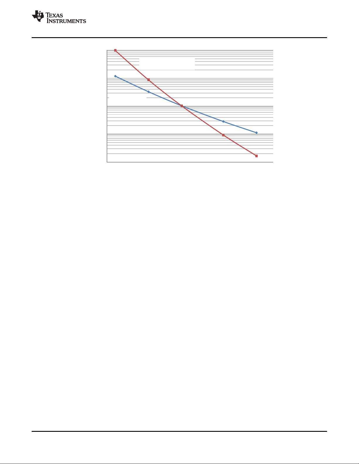
1000
10000
100000
1000000
10000000
80 90 100 110 120 130 140 150 160 170 180
Estimated Life (Hours)
Continuous T (°C)
J
EM Failure Mode
Wirebond Voiding Fail
Mode
PGA309-HT
www.ti.com
(1) See datasheet for absolute maximum and minimum recommended operating conditions.
(2) Silicon operating life design goal is 10 years at 105°C junction temperature (does not include package interconnect
life).
(3) The predicted operating lifetime vs. junction temperature is based on reliability modeling using electromigration as the
dominant failure mechanism affecting device wearout for the specific device process and design characteristics.
(4) This device is qualified for 1000 hours of continuous operation at maximum rated temperature.
SBOS687A –OCTOBER 2013–REVISED DECEMBER 2013
Figure 1. PGA309-HT Operating Life Derating Chart
Copyright © 2013, Texas Instruments Incorporated Submit Documentation Feedback 9
Product Folder Links: PGA309-HT

1
2
3
4
5
6
7
8
16
15
14
13
12
11
10
9
V
EXC
GND
A
V
SA
V
IN1
V
IN2
V
FB
V
OUT
V
SJ
TEST
V
SD
GND
D
PRG
SCL
SDA
TEMP
IN
REF /REF
IN OUT
PGA309-HT
SBOS687A –OCTOBER 2013–REVISED DECEMBER 2013
www.ti.com
PIN CONFIGURATION
PW PACKAGE
TSSOP-16
(TOP VIEW)
PIN DESCRIPTIONS
PIN NO. NAME DESCRIPTION
1 V
EXC
2 GND
3 V
4 V
5 V
6 V
7 V
8 V
SA
IN1
IN2
FB
OUT
SJ
9 TEST Test/External controller mode pin. Pull to GNDDin normal mode.
10 V
SD
11 GND
12 PRG single wire. Can be connected to V
13 SCL calibration and configuration from external EEPROM. Can also communicate directly to the registers in
14 SDA calibration and configuration from external EEPROM. Can also communicate directly to the registers in
15 TEMP
10 Submit Documentation Feedback Copyright © 2013, Texas Instruments Incorporated
16 REFIN/REF
Bridge sensor excitation. Connect to bridge if linearization and/or internal reference for bridge excitation
is to be used.
Analog ground. Connect to analog ground return path for VSA. Should be same as GNDD.
A
Analog voltage supply. Connect to analog voltage supply. To be within 200mV of VSD.
Signal input voltage 1. Connect to + or – output of sensor bridge. Internal multiplexer can change
connection internally to Front-End PGA.
Signal input voltage 2. Connect to + or – output of sensor bridge. Internal multiplexer can change
connection internally to Front-End PGA.
V
feedback pin. Voltage feedback sense point for over/under-scale limit circuitry. When internal gain
OUT
set resistors for the output amplifier are used, this is also the voltage feedback sense point for the
output amplifier. VFBin combination with VSJallows for ease of external filter and protection circuits
without degrading the PGA309 V
point of feedback for V
, if external protection is used.
OUT
accuracy. VFBmust always be connected to either V
OUT
Analog output voltage of conditioned sensor.
Output amplifier summing junction. Use for output amplifier compensation when driving large capacitive
loads (> 100pF) and/or for using external gain setting resistors for the output amplifier.
Digital voltage supply. Connect to digital voltage supply. To be within 200mV of VSA.
Digital ground. Connect to digital ground return path for VSD. Should be same as GNDA.
D
Single-wire interface program pin. UART-type interface for digital calibration of the PGA309 over a
assembly.
for a three-lead (VS, GND, V
OUT
) digitally-programmable sensor
OUT
Clock input/output for Two-Wire, industry-standard compatible interface for reading and writing digital
the PGA309 through the Two-Wire, industry-standard compatible interface.
Data input/output for Two-Wire, industry-standard compatible interface for reading and writing digital
the PGA309 through the Two-Wire, industry-standard compatible interface.
External temperature signal input. PGA309 can be configured to read a bridge current sense resistor
as an indicator of bridge temperature, or an external temperature sensing device such as diode
junction, RTD, or thermistor. This input can be internally gained by 1, 2, 4, or 8. In addition, this input
IN
can be read differentially with respect to V
internal, register-selectable, 7μA current source (I
thermistor, or diode excitation source.
GNDA
, V
, or the internal/external V
EXC
) that can be connected to TEMPINas an RTD,
TEMP
. There is also an
REF
Reference input/output pin. As an output, the internal reference (selectable as 2.5V or 4.096V) is
available for system use on this pin. As an input, the internal reference may be disabled and an
OUT
external reference can then be applied as the reference for the PGA309.
Product Folder Links: PGA309-HT
OUT
or the

90
80
70
60
50
40
30
20
10
0
-10
Frequency (Hz)
PSRR (dB)
10 100 1k 10k 100k 1M
Small-Signal
V and V Enabled
V = 2.5V
PSRR at V
REF EXT
REF
OUT
80
60
40
20
0
Frequency (Hz)
Gain (dB)
10 100 1k 10k 100k 1M
G = Output Amplifier Gain
OUTAMP
G = 9V/V
G = 128V/V
OUTAMP
FRONT
G = 9V/V
G = 32V/V
OUTAMP
FRONT
G = 2V/V
G = 32V/V
OUTAMP
FRONT
G = 2V/V
G = 8V/V
OUTAMP
FRONT
Temperature ( C)°
-55 -35 -15 5 25 45 65 85 105 125 145
9
8
7
6
5
4
3
2
1
0
Average
I ( A)m
TEMP
70
60
50
40
30
20
10
0
-10
-20
-30
Frequency (Hz)
CMRR (dB)
10 100 1k 10k 100k 1M
RTO of Front- End PGA
Average
4.090
4.085
4.080
4.075
4.070
4.065
4.060
Temperature ( C)°
-55 -35 -15 5 25 45 65 85 105 125 145
V
REF
(V)
Temperature ( C)°
-55 -35 -15 5 25 45 65 85 105 125 145
1.0
0.5
0
-0.5
-1.0
-1.5
-2.0
-2.5
-3.0
Average, nA
I (nA)
B
PGA309-HT
www.ti.com
At TA= +25°C, VSA= VSD= +5V (VSA= V
V
V
vs TEMPERATURE IBCURRENT vs TEMPERATURE
REF
Figure 2. Figure 3.
I
CURRENT vs TEMPERATURE COMMON-MODE REJECTION RATIO vs FREQUENCY
TEMP
TYPICAL CHARACTERISTICS
SUPPLY ANALOG
= REFIN/REF
REF
, VSD= V
OUT
SUPPLY DIGITAL
= +5V, unless otherwise noted.
SBOS687A –OCTOBER 2013–REVISED DECEMBER 2013
, VSAmust equal VSD), GNDD= GNDA= 0, and
Figure 4. Figure 5.
POWER-SUPPLY REJECTION RATIO vs FREQUENCY CLOSED−LOOP GAIN vs FREQUENCY
Copyright © 2013, Texas Instruments Incorporated Submit Documentation Feedback 11
Figure 6. Figure 7.
Product Folder Links: PGA309-HT

1s/div
50 V/divm
Measured After Bandpass Filter
0.1Hz Second-Order High-Pass
10Hz Fourth-Order Low-Pass
V = 4.096V
REF
1s/div
1mV/div
Measured After Bandpass Filter
0.1Hz Second-Order High-Pass
10Hz Fourth-Order Low-Pass
V = +61mV
CLK_CFG = 00 (default)
IN
G = 1152
Coarse Offset = 59mV-
Actual Die Temperature ( C)°
-55 -35 -15 5 25 45 65 85 105 125 145
0.4
0.2
0
-0.2
-0.4
-0.6
-0.8
-1.0
-1.2
Temp ADC Error ( C)°
-100 -80 -60 -40 -20 0 20 40 60 80 100
0.4
0.3
0.2
0.1
0
-0.1
-0.2
-0.3
-0.4
Total Error (% of FS)
Input Signal (% FS of V )
REF
Reg 6 = 0433h
V = 2.5V Internal
15-Bit + Sign
REF
Reg 6 = 0430h
V = 2.5V Internal
11-Bit + Sign
REF
Reg 6 = 0403h
V = 5V Internal
15-Bit + Sign
REF
Reg 6 = 0503h
V = 2.048V Internal
(Temp ADC Internal)
15-Bit + Sign
REF
Temperature ( C)°
-55 -35 -15 5 25 45 65 85 105 125 145
1.6
1.4
1.2
1.0
0.8
0.6
0.4
0.2
0
All Blocks Enabled
Ref, Exc, and ADC Disabled
I (mA)
Q
0 5 10 15 20 25
V
S
V 0.1
S
S
S
S
S
-
-
-
-
-
V 0.2
V 0.3
V 0.4
V 0.5
0.5
0.4
0.3
0.2
0.1
0
VS= 2.7V
V = 2.7V
S
V = 5V
S
V = 5V
S
I (mA)
LOAD
PGA309-HT
SBOS687A –OCTOBER 2013–REVISED DECEMBER 2013
TYPICAL CHARACTERISTICS (continued)
At TA= +25°C, VSA= VSD= +5V (VSA= V
V
= REFIN/REF
REF
TEMPERATURE ADC ERROR (INTERNAL MODE) TEMPERATURE ADC ERROR (EXTERNAL MODES)
= +5V, unless otherwise noted.
OUT
V
SWING TO RAIL vs I
OUT
Figure 8. Figure 9.
SUPPLY ANALOG
LOAD
, VSD= V
SUPPLY DIGITAL
www.ti.com
, VSAmust equal VSD), GNDD= GNDA= 0, and
IQvs TEMPERATURE
V
(0.1Hz TO 10Hz) (0.1Hz TO 10Hz PEAK-TO-PEAK NOISE)
12 Submit Documentation Feedback Copyright © 2013, Texas Instruments Incorporated
Figure 10. Figure 11.
NOISE V
REF
OUT
NOISE
Figure 12. Figure 13.
Product Folder Links: PGA309-HT

Gain = 256
Time (10 s/div)m
V (50mV/div)
OUT
Gain = 8
Time (10 s/div)m
V (50mV/div)
OUT
Gain = 1152
Time (10 s/div)m
V (500mV/div)
OUT
Time (10 s/div)m
Gain = 8
V (500mV/div)
OUT
10k 100k1k1
1
0.1
0.01
10 100
Frequency (Hz)
e ( V/ ), RTIm
ND
HzÖ
Coarse Offset Adjust = 0mV
CLK_CFG = 00 (default)
10k 50k1k1
10
1
0.1
0.01
10 100
Frequency (Hz)
e ( V/ ), RTIm
ND
HzÖ
Coarse Offset Adjust = 59mV
V = +61mV
CLK_CFG = 00 (default)
-
IN
PGA309-HT
www.ti.com
TYPICAL CHARACTERISTICS (continued)
At TA= +25°C, VSA= VSD= +5V (VSA= V
V
= REFIN/REF
REF
= +5V, unless otherwise noted.
OUT
INPUT VOLTAGE NOISE DENSITY INPUT VOLTAGE NOISE DENSITY
Figure 14. Figure 15.
LARGE-SIGNAL STEP RESPONSE LARGE-SIGNAL STEP RESPONSE
SUPPLY ANALOG
, VSD= V
SUPPLY DIGITAL
SBOS687A –OCTOBER 2013–REVISED DECEMBER 2013
, VSAmust equal VSD), GNDD= GNDA= 0, and
Copyright © 2013, Texas Instruments Incorporated Submit Documentation Feedback 13
Figure 16. Figure 17.
SMALL-SIGNAL STEP RESPONSE SMALL-SIGNAL STEP RESPONSE
Figure 18. Figure 19.
Product Folder Links: PGA309-HT

20
15
10
5
0
-5
-10
-15
-20
Error (LSB)
Code (LSB)
7000010000 20000 30000 40000 60000500000
1k
Frequency (Hz)
Phase ( )°
10k 100k 1M 10M0.1
120
100
80
60
40
20
0
45
0
-45
-90
-135
-180
-225
1 10 100
A (dB)
OL
C = 100pF
R = 4.7kW
L
L
20
15
10
5
0
-5
-10
-15
-20
Error (LSB)
Code (LSB)
7000010000 20000 30000 40000 60000500000
Unit 1
Unit 2
0 500 1000 1500 2000 2500
25
20
15
10
5
0
0.5% Settling Time ( s)m
C (pF)
LOAD
G = 9V/V
OUTAMP
G = 3.6V/V
OUTAMP
G = 2V/V
OUTAMP
Time (100 s/div)m
V (200mV/div), V (1V/div)
IN OUT
V
IN
V
OUT
PGA309-HT
SBOS687A –OCTOBER 2013–REVISED DECEMBER 2013
TYPICAL CHARACTERISTICS (continued)
At TA= +25°C, VSA= VSD= +5V (VSA= V
V
= REFIN/REF
REF
OPEN-LOOP GAIN/PHASE vs FREQUENCY ZERO DAC TYPICAL ERROR vs CODE
= +5V, unless otherwise noted.
OUT
CAPACITIVE LOAD DRIVE OVERVOLTAGE RECOVERY
Figure 20. Figure 21.
OUTPUT AMPLIFIER
SUPPLY ANALOG
, VSD= V
SUPPLY DIGITAL
www.ti.com
, VSAmust equal VSD), GNDD= GNDA= 0, and
Figure 22. Figure 23.
14 Submit Documentation Feedback Copyright © 2013, Texas Instruments Incorporated
GAIN DAC TYPICAL ERROR vs CODE
Product Folder Links: PGA309-HT
Figure 24.

PGA309-HT
www.ti.com
FUNCTIONAL DESCRIPTION
OVERVIEW
The PGA309 is a programmable analog signal
conditioner designed for resistive bridge sensor
applications. It is a complete signal conditioner with
bridge excitation, initial span and offset adjustment,
temperature adjustment of span and offset,
internal/external temperature measurement capability,
output over-scale and under-scale limiting, fault
detection, and digital calibration. The PGA309, in a
calibrated sensor module, can reduce errors to the
level approaching the bridge sensor repeatability. See
Figure 25 for a block diagram of the PGA309.
Following is a brief overview of each major function.
SENSOR ERROR ADJUSTMENT RANGE
The adjustment capability of the PGA309 is
summarized in Table 1.
Table 1. PGA309 Adjustment Capability
FSS (full-scale sensitivity) 1mV/V to 245mV/V
Span TC Over ±3300ppmFS/°C
Span TC nonlinearity ≥ 10%
Zero offset ±200%FS
Zero offset TC Over ±3000ppmFS/°C
Zero offset TC nonlinearity ≥ 10%
Sensor impedance Down to 200Ω
(2)
(1)
(2)
(3)
1. Depends on the temperature sensing scheme.
2. Combined coarse and fine offset adjust.
3. Lower impedance possible by using a dropping
resistor in series with the bridge.
GAIN SCALING
The core of the PGA309 is the precision low-drift and
no 1/f noise Front-End PGA. The overall gain of the
Front-End PGA + Output Amplifier can be adjusted
from 2.7V/V to 1152V/V. The polarity of the inputs
can be switched through the 2x2 input mux to
accommodate sensors with unknown polarity output.
The Front-End PGA provides initial coarse signal gain
using a no 1/f noise, auto-zero instrumentation
amplifier. The fine gain adjust is accomplished by the
16-bit attenuating Gain Digital-to-Analog Converter
(Gain DAC). This Gain DAC is controlled by the data
in the Temperature Compensation Lookup Table
driven by the Temperature Analog-to-Digital
SBOS687A –OCTOBER 2013–REVISED DECEMBER 2013
Converter (Temp ADC). In order to compensate for
second-order and higher drift nonlinearity, the span
drift can be fitted to piecewise linear curves during
calibration with the coefficients stored in an external
nonvolatile EEPROM lookup table.
Following the fine gain adjust stage is the Output
Amplifier that provides additional programmable gain.
Two key output amplifier connections, VFBand VSJ,
are brought out on the PGA309 for application
flexibility. These connections allow for an accurate
conditioned signal voltage while also providing a
means for PGA309 output overvoltage and large
capacitive loading for RFI/EMI filtering required in
many end applications.
OFFSET ADJUSTMENT
The sensor offset adjustment is performed in two
stages. The input-referred Coarse Offset Adjust DAC
has approximately a ±60mV offset adjustment range
for a selected V
of 5V. The fine offset and the
REF
offset drift are canceled by the 16-bit Zero DAC that
sums the signal with the output of the front-end
instrumentation amplifier. Similar to the Gain DAC,
the input digital values of the Zero DAC are controlled
by the data in the Temperature Compensation
Lookup Table, stored in external EEPROM, driven by
the Temp ADC. The programming range of the Zero
DAC is 0V to V
with an output range of 0.1V to
REF
VSA– 0.1V.
VOLTAGE REFERENCE
The PGA309 contains a precision low-drift voltage
reference (selectable for 2.5V or 4.096V) that can be
used for external circuitry through the REFIN/REF
OUT
pin. This same reference is used for the Coarse
Offset Adjust DAC, Zero DAC, Over/Under-Scale
Limits and sensor excitation/linearization through the
V
pin. When the internal reference is disabled, the
EXC
REFIN/REF
pin should be connected to an
OUT
external reference or to VSAfor ratiometric-scaled
systems.
SENSOR EXCITATION AND LINEARIZATION
A dedicated circuit with a 7-bit + sign DAC for sensor
voltage excitation and linearization is provided on the
PGA309. This block scales the reference voltage and
sums it with a portion of the PGA309 output to
compensate the positive or negative bow-shaped
nonlinearity exhibited by many sensors over their
applied pressure range. Sensors not requiring
linearization can be connected directly to the supply
(VSA) or to the V
(Lin DAC) set to zero.
pin with the Linearization DAC
EXC
Copyright © 2013, Texas Instruments Incorporated Submit Documentation Feedback 15
Product Folder Links: PGA309-HT

Interface and Control
Circuitry
PRG
SpanTC and OffsetTC Adjust Lookup
Table with interpolation
Output Coarse
Gain Adjust
(2 to 9)
2x2 Multiplexer
Int/Ext
Feedback
PGA309
+5V
Test Logic
Fault Conditions
Monitoring Circuit
Temp ADC
Signals Mux
Temperature
ADC
Linearization
DAC
Fault
Out
Fine Gain
Adjust
Fine Offset
Adjust
Front-End
PGA Out
TEST
Fault Out
SDA
SCL
Temperature ADC
Input Select
Internal
Temp Sense
Zero
DAC
Gain
DAC
Output
Amp
+5V
S
V
SD
V
REF
V
FB
V
FB
R
TEMP
GND
A
GND
D
V
FB
V
SJ
V
OUT
V
EXC
TEMP
IN
V
IN1
V
IN2
V
TEMP
V
OS
V
OUT
V
OUT
V
OUT FILT
K
LIN
K
REF
V
SA
REFIN/REF
OUT
R
ISO
100W
R
FB
100W
Power-On
Reset
Band-Gap
Voltage
Reference
Two-Wire
EEPROM
(SOT23-5)
Over-/Under-
Scale Limits
Front-End PGA
(Gain 4 to 128)
C
L
10nF
C
F
150pF
Bridge
Sensor
Coarse
Offset Adjust
PGA309-HT
SBOS687A –OCTOBER 2013–REVISED DECEMBER 2013
www.ti.com
Figure 25. Simplified Diagram of the PGA309 in a Typical Configuration
16 Submit Documentation Feedback Copyright © 2013, Texas Instruments Incorporated
Product Folder Links: PGA309-HT

PGA309-HT
www.ti.com
SBOS687A –OCTOBER 2013–REVISED DECEMBER 2013
ADC FOR TEMPERATURE SENSING algorithm for accurate DAC adjustments between
The temperature sense circuitry drives the
compensation for the sensor span and offset drift.
Either internal or external temperature sensing is
possible. The temperature can be sensed in one of
the following ways: If either Checksum1, Checksum2, or both are
• Bridge impedance change (excitation current
sense, in the positive or negative part of the
bridge), for sensors with large temperature
coefficient of resistance (TCR > 0.1%/°C).
• On-chip PGA309 temperature, when the chip is
located sufficiently close to the sensor.
• External diode, thermistor, or RTD placed on the
sensor membrane. An internal 7μA current source
may be enabled to excite these types of
temperature sensors.
The temperature signal is digitized by the onboard
Temp ADC. The output of the Temp ADC is used by
the control digital circuit to read the data from the
Lookup Table in an external EEPROM, and set the
output of the Gain DAC and the Zero DAC to the
calibrated values as temperature changes.
An additional function provided through the Temp
ADC is the ability to read the V
pin back through
OUT
the Temp ADC input mux. This provides flexibility for
a digital output through either One-Wire or Two-Wire
interface, as well as the possibility for an external
microcontroller to perform real-time custom
calibration of the PGA309.
EXTERNAL EEPROM AND TEMPERATURE COEFFICIENTS
The PGA309 uses an industry-standard Two-Wire
external EEPROM (typically, a SOT23-5 package). A
1k-bit (minimum) EEPROM is needed when using all
17 temperature coefficients. Larger EEPROMs may
be used to provide space for a serial number, lot
code, or other data.
The first part of the external EEPROM contains the
configuration data for the PGA309, with settings for:
• Register 3—Reference Control and Linearization
• Register 4—PGA Coarse Offset and Gain/Output
Amplifier Gain
• Register 5—PGA Configuration and Over/UnderScale Limit
• Register 6—Temp ADC Control
This section of the EEPROM contains its own
individual checksum (Checksum1).
The second part of the external EEPROM contains
up to 17 temperature index values and corresponding
temperature coefficients for the Zero DAC and Gain
DAC adjustments with measured temperature, and
also contains its own checksum (Checksum2). The
PGA309 lookup logic contains a linear interpolation
stored temperature indexes. This approach allows for
a piecewise linear temperature compensation of up to
17 temperature indexes and associated temperature
coefficients.
incorrect, the output of the PGA309 is set to highimpedance.
FAULT MONITOR
To detect sensor burnout or a short, a set of four
comparators are connected to the inputs of the FrontEnd PGA. If any of the inputs are taken to within
100mV of ground or V
, or violate the input CMR of
EXC
the Front-End PGA, then the corresponding
comparator sets a sensor fault flag that causes the
PGA309 V
to be driven within 100mV of either V
OUT
SA
or ground, depending upon the alarm configuration
setting (Register 5—PGA Configuration and
Over/Under-Scale Limit). This will be well above the
set Over-Scale Limit level or well below the set
Under-Scale Limit level. The state of the fault
condition can be read in digital form in Register
8—Alarm Status Register. If the Over/Under-Scale
Limit is disabled, the PGA309 output voltage will still
be driven within 100mV of either VSAor ground,
depending upon the alarm configuration setting.
There are five other fault detect comparators that
help detect subtle PGA309 front-end violations that
could otherwise result in linear voltages at V
OUT
that
would be interpreted as valid states. These are
especially useful during factory calibration and setup,
and are configured through Register 5—PGA
Configuration and Over/Under-Scale Limit. The
respective status of each can also be read back
through Register 8—Alarm Status Register.
OVER-SCALE AND UNDER-SCALE LIMITSE
The over-scale and under-scale limit circuitry
combined with the fault monitor circuitry provides a
means for system diagnostics. A typical sensorconditioned output may be scaled for 10% to 90% of
the system ADC range for the sensor normal
operating range. If the conditioned pressure sensor is
below 4%, it is considered under-pressure; if over
96%, it is considered over-pressure.
The PGA309 over/under-scale limit circuit can be
programmed individually for under-scale and overscale values that clip or limit the PGA309 output.
From a system diagnostic view, 10% to 90% of ADC
range is normal operation, less than 4% is underpressure, and greater than 96% is over-pressure. If
the fault detect circuitry is used, a detected fault will
cause the PGA309 output to be driven to positive or
negative saturation.
Copyright © 2013, Texas Instruments Incorporated Submit Documentation Feedback 17
Product Folder Links: PGA309-HT

V = mux_sign V + V GI + V GD GO
OUT IN Coarse_Offset Zero_DAC
[ ]? ? ? ?
(
(
PGA309-HT
SBOS687A –OCTOBER 2013–REVISED DECEMBER 2013
If this fault flag is programmed for high, then greater DIGITAL INTERFACE than 97% ADC range will be a fault; if programmed for low. then less than 3% ADC range will be a fault. In this configuration, the system software can be used to distinguish between over- or under-pressure condition, which indicates an out-of-control process, or a sensor fault.
POWER-UP AND NORMAL OPERATION
The PGA309 has circuitry to detect when the power
supply is applied to the PGA309, and reset the
internal registers and circuitry to an initial state. This
reset also occurs when the supply is detected to be
invalid, so that the PGA309 is in a known state when
the supply becomes valid again. The rising threshold
for this circuit is typically 2.2V and the falling
threshold is typically 1.7V. After the power supply
becomes valid, the PGA309 waits for approximately
25ms and then attempts to read the configuration
data from the external EEPROM device.
If the EEPROM has the proper flag set in address
locations 0 and 1, then the PGA309 continues
reading the first part of the EEPROM; otherwise, the
PGA309 waits for one second before trying again. If
the PGA309 detects no response from the EEPROM,
the PGA309 waits for one second and tries again;
otherwise, the PGA309 tries to free the bus and waits
for 25ms before trying to read the EEPROM again. If
a successful read of the first part of the EEPROM is
accomplished, (including valid Checksum1 data), the
PGA309 triggers the Temp ADC to measure
temperature. For 16-bit resolution results, the
converter takes approximately 125ms to complete a
conversion. Once the conversion is complete, the
PGA309 begins reading the Lookup Table information
from the EEPROM (second part) to calculate the
settings for the Gain DAC and Zero DAC.
The PGA309 reads the entire Lookup Table so that it
There are two digital interfaces on the PGA309. The
PRG pin uses a One-Wire, UART-compatible
interface with bit rates from 4.8Kbits/s to 38.4Kbits/s.
The SDA and SCL pins together form an industry
standard Two-Wire interface at clock rates from 1kHz
to 400kHz. The external EEPROM uses the Two-Wire
interface. Communication to the PGA309 internal
registers, as well as to the external EEPROM, for
programming and readback can be conducted
through either digital interface.
It is also possible to connect the One-Wire
communication pin, PRG, to the V
three-wire sensor modules and still allow for
programming. In this mode, the PGA309 output
amplifier may be enabled for a set time period and
then disabled again to allow sharing of the PRG pin
with the V
connection. This allows for both digital
OUT
calibration and analog readback during sensor
calibration in a three-wire sensor module.
The Two-Wire interface has timeout mechanisms to
prevent bus lockup from occurring. The Two-Wire
master controller in the PGA309 has a mode that
attempts to free up a stuck-at-zero SDA line by
issuing SCL pulses, even when the bus is not
indicated as idle after a timeout period has expired.
The timeout will only apply when the master portion
of the PGA309 is attempting to initiate a Two-Wire
communication.
PGA309 TRANSFER FUNCTION
Equation 1 shows the mathematical expression that is
used to compute the output voltage, V
equation can also be rearranged algebraically to
solve for different terms. For example, during
calibration, this equation is rearranged to solve for
VIN.
can determine if the checksum for the Lookup Table
(Checksum2) is correct. Each entry in the Lookup
Table requires approximately 500μs to read from the
EEPROM. Once the checksum is determined to be
valid, the calculated values for the Gain and Zero
DACs are updated into their respective registers, and
the output amplifier is enabled. The PGA309 then
begins looping through this entire procedure, starting
with reading the EEPROM configuration registers
from the first part of the EEPROM, then starting a
new conversion on the Temp ADC, which then
triggers reading the Lookup Table data from the
second part of the EEPROM. This loop continues
indefinitely.
Where:
mux_sign: This term changes the polarity of the
input signal; value is ±1.
VIN: The input signal for the PGA309; VIN1 = V
VIN2 = V
V
Coarse_Offset
.
INN
: The coarse offset DAC output
voltage.
GI: Input stage gain.
V
Zero_DAC
: Zero DAC output voltage.
GD: Gain DAC.
GO: Output stage gain.
pin in true
OUT
www.ti.com
. This
OUT
INP
(1)
,
18 Submit Documentation Feedback Copyright © 2013, Texas Instruments Incorporated
Product Folder Links: PGA309-HT

R
4R
R
Auto
Zero
Auto
Zero
R
Auto
Zero
PGA
Diff Amp
xG
Bandgap
Reference
POR
A2
A1
A3
PGA Gain Select (1 of 8)
Range of 4 to 128
(with PGA Diff Amp Gain = 4)
RGO
Output Gain Select (1 of 7)
Range of 2 to 9
Digital Controls
SCL
PRG
SDA
x0.52
x0.83
x0.124
x0.166
INT/EXT FB Select
Alarm Register Inputs
Temp ADC
Ref Mux
Temp ADC
Internal REF
Internal
Temp Sense
16 3 10
14
13
12
7
6
8
112
9
4
5
15
1
S
Fault Monitor
Circuit
Test Logic
Temp ADC
Input Mux
Temp ADC
REF Select
Temp Select
Source
Temp ADC, PGA
(x1, x2, x4, x8)
Temp ADC Input
Mux Select
Interface and
Control Circuitry
Control Registers
Alarm Register
Offset TC Adjust and Scan TC Adjust
Look-Up Logic with Interpolation Algorithm
Output
Amplifier
Input Mux
Input Mux
Control
Coarse
Offset Adjust
Fine
Offset Adjust
Fine Gain Adjust
(16-Bit)
TEST
RFO
PGA309
V
EXC
V
EXC
V
SA
V
FB
V
SA
V
SA
V
SD
V
SD
V
REFT
V
REF
R
F
R
F
R
G
V
REF
V
REF
V
REF
V
FB
V
FB
V
OUT
V
SJ
V
IN2
V
IN1
GNDAGND
D
V
OUT
V
INP
V
INN
V
REF
V
REF
V
EXC
V
EXC
V
OUT
V
SA
I
TEMP
7 Am
16-Bit
Zero
DAC
16-Bit
4-Bit +
Sign DAC
I Enable
TEMP
V Internal Set
(2.5V or 4.096V)
REF
V Internal Set
(2.5V or 4.096V)
REF
V Enable
EXC
REF /REF
IN OUT
TEMP
IN
TEMP
IN
7-Bit + Sign
Lin DAC
15-Bit + Sign
Temp ADC
Linearization and V
Gain Adjust
EXC
V
REF
R
SET
Gain
DAC
3-Bit
DAC
Scale
Limiter
3-Bit
DAC
Over-Scale
Limit
Under-Scale
Limit
Front-End
PGA Output
Front-End PGA
PGA309-HT
www.ti.com
SBOS687A –OCTOBER 2013–REVISED DECEMBER 2013
Copyright © 2013, Texas Instruments Incorporated Submit Documentation Feedback 19
Figure 26. Detailed Block Diagram
Product Folder Links: PGA309-HT

PGA309-HT
SBOS687A –OCTOBER 2013–REVISED DECEMBER 2013
www.ti.com
REVISION HISTORY
Changes from Original (October 2013) to Revision A Page
• Changed ELECTRICAL CHARACTERISTICS table ............................................................................................................ 4
20 Submit Documentation Feedback Copyright © 2013, Texas Instruments Incorporated
Product Folder Links: PGA309-HT

PACKAGE OPTION ADDENDUM
www.ti.com
10-Dec-2020
PACKAGING INFORMATION
Orderable Device Status
PGA309ASPWT ACTIVE TSSOP PW 16 250 RoHS & Green NIPDAU Level-2-260C-1 YEAR -55 to 150 PGA
(1)
The marketing status values are defined as follows:
ACTIVE: Product device recommended for new designs.
LIFEBUY: TI has announced that the device will be discontinued, and a lifetime-buy period is in effect.
NRND: Not recommended for new designs. Device is in production to support existing customers, but TI does not recommend using this part in a new design.
PREVIEW: Device has been announced but is not in production. Samples may or may not be available.
OBSOLETE: TI has discontinued the production of the device.
Package Type Package
(1)
Drawing
Pins Package
Qty
Eco Plan
(2)
Lead finish/
Ball material
(6)
MSL Peak Temp
(3)
Op Temp (°C) Device Marking
(4/5)
309AS
(2)
RoHS: TI defines "RoHS" to mean semiconductor products that are compliant with the current EU RoHS requirements for all 10 RoHS substances, including the requirement that RoHS substance
do not exceed 0.1% by weight in homogeneous materials. Where designed to be soldered at high temperatures, "RoHS" products are suitable for use in specified lead-free processes. TI may
reference these types of products as "Pb-Free".
RoHS Exempt: TI defines "RoHS Exempt" to mean products that contain lead but are compliant with EU RoHS pursuant to a specific EU RoHS exemption.
Green: TI defines "Green" to mean the content of Chlorine (Cl) and Bromine (Br) based flame retardants meet JS709B low halogen requirements of <=1000ppm threshold. Antimony trioxide based
flame retardants must also meet the <=1000ppm threshold requirement.
(3)
MSL, Peak Temp. - The Moisture Sensitivity Level rating according to the JEDEC industry standard classifications, and peak solder temperature.
(4)
There may be additional marking, which relates to the logo, the lot trace code information, or the environmental category on the device.
(5)
Multiple Device Markings will be inside parentheses. Only one Device Marking contained in parentheses and separated by a "~" will appear on a device. If a line is indented then it is a continuation
of the previous line and the two combined represent the entire Device Marking for that device.
(6)
Lead finish/Ball material - Orderable Devices may have multiple material finish options. Finish options are separated by a vertical ruled line. Lead finish/Ball material values may wrap to two
lines if the finish value exceeds the maximum column width.
Important Information and Disclaimer:The information provided on this page represents TI's knowledge and belief as of the date that it is provided. TI bases its knowledge and belief on information
provided by third parties, and makes no representation or warranty as to the accuracy of such information. Efforts are underway to better integrate information from third parties. TI has taken and
continues to take reasonable steps to provide representative and accurate information but may not have conducted destructive testing or chemical analysis on incoming materials and chemicals.
TI and TI suppliers consider certain information to be proprietary, and thus CAS numbers and other limited information may not be available for release.
In no event shall TI's liability arising out of such information exceed the total purchase price of the TI part(s) at issue in this document sold by TI to Customer on an annual basis.
Samples
Addendum-Page 1

PACKAGE OPTION ADDENDUM
www.ti.com
OTHER QUALIFIED VERSIONS OF PGA309-HT :
Catalog: PGA309
•
NOTE: Qualified Version Definitions:
Catalog - TI's standard catalog product
•
10-Dec-2020
Addendum-Page 2

PACKAGE MATERIALS INFORMATION
www.ti.com 9-Jan-2014
TAPE AND REEL INFORMATION
*All dimensions are nominal
Device Package
Type
PGA309ASPWT TSSOP PW 16 250 180.0 12.4 6.9 5.6 1.6 8.0 12.0 Q1
Package
Drawing
Pins SPQ Reel
Diameter
(mm)
Reel
Width
W1 (mm)
A0
(mm)B0(mm)K0(mm)P1(mm)W(mm)
Pin1
Quadrant
Pack Materials-Page 1

PACKAGE MATERIALS INFORMATION
www.ti.com 9-Jan-2014
*All dimensions are nominal
Device Package Type Package Drawing Pins SPQ Length (mm) Width (mm) Height (mm)
PGA309ASPWT TSSOP PW 16 250 210.0 185.0 35.0
Pack Materials-Page 2

PACKAGE OUTLINE
A
5.1
4.9
NOTE 3
SCALE 2.500
TSSOP - 1.2 mm max heightPW0016A
SMALL OUTLINE PACKAGE
SEATING
6.6
TYP
6.2
PIN 1 INDEX AREA
1
8
B
4.5
4.3
NOTE 4
16
9
14X 0.65
2X
4.55
0.30
16X
0.19
0.1 C A B
C
1.2 MAX
PLANE
0.1 C
(0.15) TYP
SEE DETAIL A
GAGE PLANE
0.25
0.75
-80
0.50
A 20
DETAIL A
TYPICAL
4220204/A 02/2017
NOTES:
1. All linear dimensions are in millimeters. Any dimensions in parenthesis are for reference only. Dimensioning and tolerancing
per ASME Y14.5M.
2. This drawing is subject to change without notice.
3. This dimension does not include mold flash, protrusions, or gate burrs. Mold flash, protrusions, or gate burrs shall not
exceed 0.15 mm per side.
4. This dimension does not include interlead flash. Interlead flash shall not exceed 0.25 mm per side.
5. Reference JEDEC registration MO-153.
0.15
0.05
www.ti.com

EXAMPLE BOARD LAYOUT
TSSOP - 1.2 mm max heightPW0016A
SMALL OUTLINE PACKAGE
16X (0.45)
14X (0.65)
1
8
16X (1.5)
SYMM
(R0.05) TYP
16
SYMM
9
(5.8)
LAND PATTERN EXAMPLE
EXPOSED METAL SHOWN
SCALE: 10X
SOLDER MASK
OPENING
EXPOSED METAL
0.05 MAX
ALL AROUND
NON-SOLDER MASK
DEFINED
(PREFERRED)
METAL
15.000
SOLDER MASK DETAILS
METAL UNDER
SOLDER MASK
0.05 MIN
ALL AROUND
SOLDER MASK
DEFINED
NOTES: (continued)
6. Publication IPC-7351 may have alternate designs.
7. Solder mask tolerances between and around signal pads can vary based on board fabrication site.
SOLDER MASK
OPENING
EXPOSED METAL
4220204/A 02/2017
www.ti.com

EXAMPLE STENCIL DESIGN
TSSOP - 1.2 mm max heightPW0016A
SMALL OUTLINE PACKAGE
16X (0.45)
14X (0.65)
1
8
16X (1.5)
SYMM
(5.8)
SOLDER PASTE EXAMPLE
BASED ON 0.125 mm THICK STENCIL
SCALE: 10X
(R0.05) TYP
16
SYMM
9
4220204/A 02/2017
NOTES: (continued)
8. Laser cutting apertures with trapezoidal walls and rounded corners may offer better paste release. IPC-7525 may have alternate
design recommendations.
9. Board assembly site may have different recommendations for stencil design.
www.ti.com

IMPORTANT NOTICE AND DISCLAIMER
TI PROVIDES TECHNICAL AND RELIABILITY DATA (INCLUDING DATASHEETS), DESIGN RESOURCES (INCLUDING REFERENCE
DESIGNS), APPLICATION OR OTHER DESIGN ADVICE, WEB TOOLS, SAFETY INFORMATION, AND OTHER RESOURCES “AS IS”
AND WITH ALL FAULTS, AND DISCLAIMS ALL WARRANTIES, EXPRESS AND IMPLIED, INCLUDING WITHOUT LIMITATION ANY
IMPLIED WARRANTIES OF MERCHANTABILITY, FITNESS FOR A PARTICULAR PURPOSE OR NON-INFRINGEMENT OF THIRD
PARTY INTELLECTUAL PROPERTY RIGHTS.
These resources are intended for skilled developers designing with TI products. You are solely responsible for (1) selecting the appropriate
TI products for your application, (2) designing, validating and testing your application, and (3) ensuring your application meets applicable
standards, and any other safety, security, or other requirements. These resources are subject to change without notice. TI grants you
permission to use these resources only for development of an application that uses the TI products described in the resource. Other
reproduction and display of these resources is prohibited. No license is granted to any other TI intellectual property right or to any third
party intellectual property right. TI disclaims responsibility for, and you will fully indemnify TI and its representatives against, any claims,
damages, costs, losses, and liabilities arising out of your use of these resources.
TI’s products are provided subject to TI’s Terms of Sale (www.ti.com/legal/termsofsale.html) or other applicable terms available either on
ti.com or provided in conjunction with such TI products. TI’s provision of these resources does not expand or otherwise alter TI’s applicable
warranties or warranty disclaimers for TI products.
Mailing Address: Texas Instruments, Post Office Box 655303, Dallas, Texas 75265
Copyright © 2020, Texas Instruments Incorporated
 Loading...