

Page 1
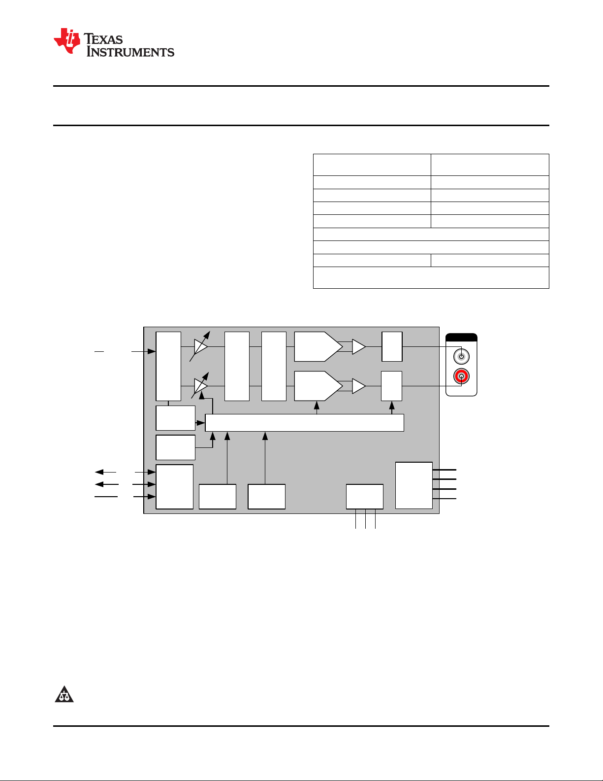
Audio Interface
8x Interpolation Filter
32bit ∆Σ Modulator
Current
Segment
DAC
Current
Segment
DAC
I/V I/V
Analog
Mute
Analog
Mute
Zero
Data
Detector
UVP/Reset
PLL Clock
Power
Supply
Ch. PumpPOR
Clock Halt
Detection
Advanced Mute Control
MCK
BCK
LRCK
CAPP
CAPM
VNEG
LINE OUT
DIN (i2s)
PCM510x
CPVDD (3.3V)
AVDD (3.3V)
DVDD (3.3V)
GND
Draft Only
PCM5100, PCM5101, PCM5102
www.ti.com
2V
1
FEATURES
23
• Market-Leading Low Out-of-Band Noise
DirectPath™, 112/106/100dB Audio Stereo DAC with 32-bit, 384kHz PCM Interface
RMS
Check for Samples: PCM5100, PCM5101, PCM5102
• Selectable Digital-Filter Latency &
Performance
• No DC Blocking Capacitors Required
• Integrated Negative Charge Pump
• Internal Pop-Free Control For Sample-Rate
Changes Or Clock Halts
• Intelligent Muting System; Soft Up/Down Ramp
& Analog Mute For 120dB Mute SNR With
Popless Operation.
• Integrated High-Performance Audio PLL With
BCK Reference To Generate SCK Internally
• Small 20-pin TSSOP Package
SLAS764A –MAY 2011–REVISED MARCH 2012
Typical Performance (3.3V Power Supply)
Parameter PCM5102 / PCM5101 /
SNR 112 / 106 / 100dB
Dynamic Range 112 / 106 / 100dB
THD+N @ - 1dBFS –93 / –92 / –90dB
Full Scale Output 2.1V
Normal 8× Oversampling Digital Filter Latency: 20/f
Low Latency 8× Oversampling Digital Filter Latency: 3.5/f
Sampling Frequency 8kHz to 384kHz
System Clock Multiples (f
768, 1024, 1152, 1536, 2048, 3072; up to 50 MHz
): 64, 128, 192, 256, 384, 512,
SCK
PCM5100
(GND center)
RMS
S
S
Figure 1. PCM510x Functional Block Diagram
OTHER KEY FEATURES
• Accepts 16-, 24-, And 32-Bit Audio Data
• PCM Data Formats: I2S, Left-Justified
• Automatic Power-Save Mode When LRCK And
BCK Are Deactivated.
• 3.3V Failsafe LVCMOS Digital Inputs
• Hardware Configuration
1
Please be aware that an important notice concerning availability, standard warranty, and use in critical applications of
Texas Instruments semiconductor products and disclaimers thereto appears at the end of this data sheet.
2System Two Cascade, Audio Precision are trademarks of Audio Precision.
3DirectPath is a trademark of Texas, Instruments, Inc..
PRODUCTION DATA information is current as of publication date.
Products conform to specifications per the terms of the Texas
Instruments standard warranty. Production processing does not
necessarily include testing of all parameters.
• Single Supply Operation:
– 3.3V Analog, 3.3V Digital
• Integrated Power-On Reset
Copyright © 2011–2012, Texas Instruments Incorporated
Page 2
PCM5100, PCM5101, PCM5102
Draft Only
SLAS764A –MAY 2011–REVISED MARCH 2012
APPLICATIONS
• A/V Receivers
• DVD, BD Players
• HDTV Receivers
• Applications Requiring 2V
Audio Output
RMS
DESCRIPTION
The PCM510x devices are a family of monolithic
CMOS integrated circuits that include a stereo digitalto-analog converter and additional support circuitry in
a small TSSOP package. The PCM510x uses the
latest generation of TI’s advanced segment-DAC
architecture to achieve excellent dynamic
performance and improved tolerance to clock jitter.
The PCM510x provides 2.1V
outputs, allowing designers to eliminate DC blocking
capacitors on the output, as well as external muting
circuits traditionally associated with single supply line
drivers.
ground centered
RMS
www.ti.com
The integrated line driver surpasses all other chargepump based line drivers by supporting loads down to
1kΩ. By supporting loads down to 1kΩ, the PCM510x
can essentially drive up to 10 products in parallel.
(LCD TV, DVDR, AV Receivers etc).
The integrated PLL on the device removes the
requirement for a system clock (commonly known as
master clock). This allows a 3-wire I2S connection,
along with reduced system EMI.
Intelligent clock error and PowerSense under voltage
protection utilizes a two level mute system for popfree performance. Upon clock error or system power
failure, the device digitally attenuates the data (or last
known good data), then mutes the analog circuit
Compared with existing DAC technology, the
PCM510x family offers up to 20dB lower out-of-band
noise, reducing EMI and aliasing in downstream
amplifiers/ADCs. (from traditional 100kHz OBN
measurements all the way to 3MHz)
The PCM510x accepts industry-standard audio data
formats with 16- to 32-bit data. Sample rates up to
384kHz are supported.
Table 1. Differences Between PCM510x Devices
Part Number Dynamic Range SNR THD
PCM5102 112dB 112dB –93dB
PCM5101 106dB 106dB –92dB
PCM5100 100dB 100dB –90dB
spacer
ABSOLUTE MAXIMUM RATINGS
over operating free-air temperature range (unless otherwise noted)
VALUE UNIT
Supply Voltage AVDD, CPVDD, DVDD –0.3 to 3.9
Digital Input Voltage –0.3 to 3.9 V
Analog Input Voltage –0.3 to 3.9
Operating Temperature Range –25 to 85
Storage Temperature Range –65 to 150
THERMAL CHARACTERISTICS
over operating free-air temperature range (unless otherwise noted)
PARAMETER TEST CONDITIONS MIN TYP MAX UNIT
θ
JA
ψ
JT
ψ
JB
θ
JC
θ
JB
Theta JA High K 91.2
Psi JT 1.0
Psi JB 41.5 ºC/W
Theta JC Top 25.3
Theta JB 42.0
°C
2 Submit Documentation Feedback Copyright © 2011–2012, Texas Instruments Incorporated
Product Folder Link(s): PCM5100 PCM5101 PCM5102
Page 3
Draft Only
PCM5100, PCM5101, PCM5102
www.ti.com
SLAS764A –MAY 2011–REVISED MARCH 2012
ELECTRICAL CHARACTERISTICS
All specifications at TA= 25°C, AVDD= CPVDD= DVDD= 3.3V, fS= 48kHz, system clock = 512 fSand 24-bit data unless
otherwise noted.
PARAMETER TEST CONDITIONS MIN TYP MAX UNIT
Resolution 16 24 32 Bits
Data Format (PCM Mode)
Audio data interface format I2S, left justified
Audio data bit length 16, 24, 32-bit acceptable
Audio data format MSB First, 2’s Complement
f
S
Digital Input/Output
V
IH
V
IL
I
IH
I
IL
V
OH
V
OL
Sampling frequency 8 384 kHz
System clock frequency 64, 128, 192, 256, 384, 512, 768, 1024, 1152, 1536, 2048, or
3072
f
, up to 50Mhz
SCK
Logic Family: 3.3V LVCMOS compatible
0.7×DV
Input logic level V
VIN= V
Input logic current µA
Output logic level V
DD
VIN= 0V –10
IOH= –4mA 0.8×DV
IOL= 4mA 0.22×DV
DD
DD
0.3×DV
DD
10
DD
Copyright © 2011–2012, Texas Instruments Incorporated Submit Documentation Feedback 3
Product Folder Link(s): PCM5100 PCM5101 PCM5102
Page 4
PCM5100, PCM5101, PCM5102
Draft Only
SLAS764A –MAY 2011–REVISED MARCH 2012
www.ti.com
ELECTRICAL CHARACTERISTICS (continued)
All specifications at TA= 25°C, AVDD= CPVDD= DVDD= 3.3V, fS= 48kHz, system clock = 512 fSand 24-bit data unless
otherwise noted.
PARAMETER TEST CONDITIONS MIN TYP MAX UNIT
Dynamic Performance (PCM Mode)
THD+N at –1 dBFS
Dynamic range
(2)
Signal-to-noise ratio
Signal to noise ratio with EIAJ, A-weighted, fS= 48kHz 113 123
analog mute
(2)(3)
Channel Separation fS= 48 kHz 100/ 95/ 90 109/103/97
Analog Output
Output voltage 2.1 V
Gain error –6 ±2.0 6 % of FSR
Gain mismatch, channel-to- –6 ±2.0 6
channel
Bipolar zero error At bipolar zero –5 ±1.0 5 mV
Load impedance 1 kΩ
Filter Characteristics–1: Normal
Pass band 0.45f
Stop band 0.55f
Stop band attenuation –60
Pass-band ripple ±0.02
Delay time 20/f
Filter Characteristics–2: Low Latency
Pass band 0.47f
Stop band 0.55f
Stop band attenuation –52
Pass-band ripple ±0.0001
Delay time 3.5/f
(1) Filter condition: THD+N: 20Hz HPF, 20kHz AES17 LPF Dynamic range: 20Hz HPF, 20kHz AES17 LPF, A-weighted Signal-to-noise
ratio: 20Hz HPF, 20kHz AES17 LPF, A-weighted Channel separation: 20Hz HPF, 20kHz AES17 LPF Analog performance specifications
are measured using the System Two Cascade™ audio measurement system by Audio Precision™ in the RMS mode.
(2) Output load is 10kΩ, with 470Ω output resistor and a 2.2nF shunt capacitor (see recommended output filter).
(3) Assert XSMT or both L-ch and R-ch PCM data are BPZ
(1)(2)
(Values shown for three devices PCM5102/PCM5101/PCM5100)
fS= 48kHz –93/–92/–90 -83/ -82/ -80
(2)
fS= 96kHz –93/–92/–90
fS= 192kHz –93/–92/–90
EIAJ, A-weighted, fS= 48kHz 106/ 100/ 95 112/106/100
EIAJ, A-weighted, fS= 96kHz 112/106/100
EIAJ, A-weighted, fS= 192kHz 112/106/100
(2)
EIAJ, A-weighted, fS= 48kHz 112/106/100 dB
EIAJ, A-weighted, fS= 96kHz 112/106/100
EIAJ, A-weighted, fS= 192kHz 112/106/100
EIAJ, A-weighted, fS= 96kHz 123
EIAJ, A-weighted, fS= 192kHz 123
fS= 96kHz 109/103/97
fS= 192kHz 109/103/97
% of FSR
S
S
dB
S
S
S
dB
S
RMS
s
s
4 Submit Documentation Feedback Copyright © 2011–2012, Texas Instruments Incorporated
Product Folder Link(s): PCM5100 PCM5101 PCM5102
Page 5
Draft Only
PCM5100, PCM5101, PCM5102
www.ti.com
SLAS764A –MAY 2011–REVISED MARCH 2012
ELECTRICAL CHARACTERISTICS (continued)
All specifications at TA= 25°C, AVDD= CPVDD= DVDD= 3.3V, fS= 48kHz, system clock = 512 fSand 24-bit data unless
otherwise noted.
PARAMETER TEST CONDITIONS MIN TYP MAX UNIT
Power Supply Requirements
DV
AV
CPV
I
DD
I
DD
I
DD
I
CC
I
CC
I
CC
DD
DD
Digital supply voltage Target DVDD= 3.3V 3.0 3.3 3.6
Analog supply voltage 3.0 3.3 3.6 VDC
Charge-pump suply voltage 3.0 3.3 3.6
DD
fS= 48kHz 7 12
DVDDsupply current at 3.3V
(4)
fS= 96kHz 8 mA
fS= 192kHz 9
fS= 48kHz 8 13
DVDDsupply current at 3.3V
(5)
fS= 96kHz 9 mA
fS= 192kHz 10
DVDDsupply current at 3.3V
(6)
0.5 0.8 mA
fS= 48kHz 11 16
AVDD/ CPVDDSupply
(4)
Current
fS= 96kHz 11 mA
fS= 192kHz 11
fS= 48kHz 22 32
AVDD/ CPVDDSupply
(5)
Current
fS= 96kHz 22 mA
fS= 192kHz 22
AVDD/ CPVDDSupply fS= n/a 0.2 0.4
(6)
Current
fS= 48kHz 59.4 92.4
Power Dissipation, DVDD=
(4)
3.3V
fS= 96kHz 62.7 mW
fS= 192kHz 66.0
fS= 48kHz 99.0 148.5
Power Dissipation, DVDD=
(5)
3.3V
fS= 96kHz 102.3 mW
fS= 192kHz 105.6
Power Dissipation, DVDD= fS= n/a (Power Down Mode) 2.3 4.0
(6)
3.3V
mA
mW
(4) Input is Bipolar Zero data.
(5) Input is 1kHz -1dBFS data
(6) Power Down Mode
Copyright © 2011–2012, Texas Instruments Incorporated Submit Documentation Feedback 5
Product Folder Link(s): PCM5100 PCM5101 PCM5102
Page 6
PCM5100, PCM5101, PCM5102
Draft Only
SLAS764A –MAY 2011–REVISED MARCH 2012
TERMINAL FUNCTIONS, PCM510x
Table 2. TERMINAL FUNCTIONS, PCM510x
TERMINAL
NAME NO.
CPVDD 1 — Charge pump power supply, 3.3V
CAPP 2 O Charge pump flying capacitor terminal for positive rail
CPGND 3 — Charge pump ground
CAPM 4 O Charge pump flying capacitor terminal for negative rail
VNEG 5 O Negative charge pump rail terminal for decoupling, -3.3V
OUTL 6 O Analog output from DAC left channel
OUTR 7 O Analog output from DAC right channel
AVDD 8 -— Analog power supply, 3.3V
AGND 9 — Analog ground
DEMP 10 I De-emphasis control for 44.1kHz sampling rate
FLT 11 I Filter select : Normal latency (Low) / Low latency (High)
SCK 12 I System clock input
BCK 13 I Audio data bit clock input
DIN 14 I Audio data input
LRCK 15 I Audio data word clock input
FMT 16 I Audio format selection : I2S (Low) / Left justified (High)
XSMT 17 I Soft mute control
LDOO 18 — Internal logic supply rail terminal for decoupling
DGND 19 — Digital ground
DVDD 20 — Digital power supply, 3.3V
(1) Failsafe LVCMOS Schmitt trigger input
I/O DESCRIPTION
DEVICE INFORMATION
PCM510X (top view)
(1)
(1)
(1)
(1)
(1)
: Soft mute (Low) / soft un-mute (High)
(1)
: Off (Low) / On (High)
www.ti.com
6 Submit Documentation Feedback Copyright © 2011–2012, Texas Instruments Incorporated
Product Folder Link(s): PCM5100 PCM5101 PCM5102
Page 7
-10
10
-110
-90
-70
-50
-30
-100 -80 -60 -40 -20 0
Input Level [dBFS]
THD+N [dB]
-110
-90
-70
-50
-30
-10
10
-100 -80 -60 -40 -20 0
Input Level [dBFS]
THD+N [dB]
-110
-90
-70
-50
-30
-10
10
-100 -80 -60 -40 -20 0
Input Level [dBFS]
THD+N [dB]
Draft Only
PCM5100, PCM5101, PCM5102
www.ti.com
SLAS764A –MAY 2011–REVISED MARCH 2012
TYPICAL CHARACTERISTICS
All specifications at TA= 25°C, AVDD= CPVDD= DVDD= 3.3V, fS= 48kHz, system clock = 512 fSand 24-bit data unless
otherwise noted.
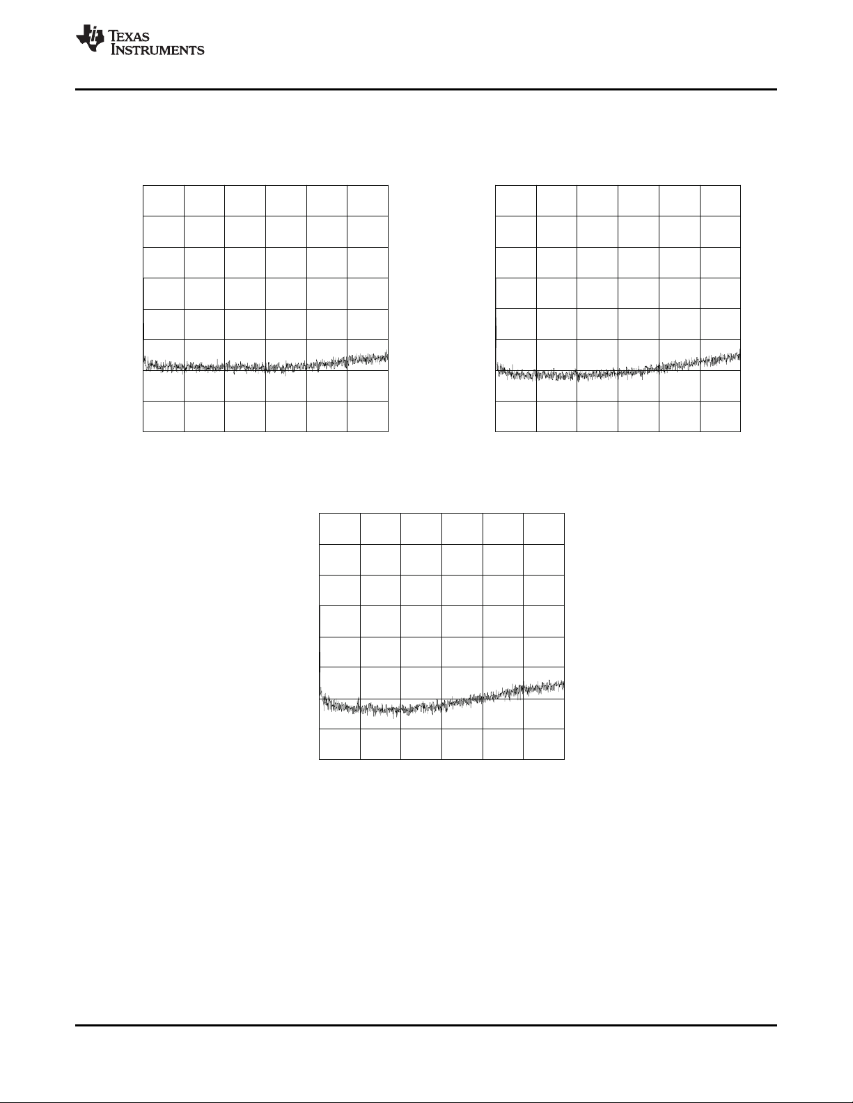
PCM5100 THD+N PCM5101 THD+N
vs vs
Input Level Input Level
Figure 2. Figure 3.
PCM5102 THD+N
vs
Input Level
Figure 4.
Copyright © 2011–2012, Texas Instruments Incorporated Submit Documentation Feedback 7
Product Folder Link(s): PCM5100 PCM5101 PCM5102
Page 8
-180
-160
-140
-120
-100
-80
-60
-40
-20
0 5 10 15 20
Frequency [kHz]
Amplitude [dB]
-180
-160
-140
-120
-100
-80
-60
-40
-20
0 5 10 15 20
Frequency [kHz]
Amplitude [dB]
-180
-160
-140
-120
-100
-80
-60
-40
-20
0 5 10 15 20
Frequency [kHz]
Amplitude [dB]
PCM5100, PCM5101, PCM5102
Draft Only
SLAS764A –MAY 2011–REVISED MARCH 2012
www.ti.com
TYPICAL CHARACTERISTICS (continued)
All specifications at TA= 25°C, AVDD= CPVDD= DVDD= 3.3V, fS= 48kHz, system clock = 512 fSand 24-bit data unless
otherwise noted.
PCM5100 FFT Plot at BPZ With AMUTE PCM5101 FFT Plot at BPZ With AMUTE
Figure 5. Figure 6.
PCM5102 FFT Plot at BPZ With AMUTE
Figure 7.
8 Submit Documentation Feedback Copyright © 2011–2012, Texas Instruments Incorporated
Product Folder Link(s): PCM5100 PCM5101 PCM5102
Page 9
-160
-140
-120
-100
-80
-60
-40
-20
0
0 50 100 150 200 250 300
Frequency [kHz]
Amplitude [dB]
-160
-140
-120
-100
-80
-60
-40
-20
0
0 50 100 150 200 250 300
Frequency [kHz]
Amplitude [dB]
-160
-140
-120
-100
-80
-60
-40
-20
0
0 50 100 150 200 250 300
Frequency [kHz]
Amplitude [dB]
Draft Only
PCM5100, PCM5101, PCM5102
www.ti.com
SLAS764A –MAY 2011–REVISED MARCH 2012
TYPICAL CHARACTERISTICS (continued)
All specifications at TA= 25°C, AVDD= CPVDD= DVDD= 3.3V, fS= 48kHz, system clock = 512 fSand 24-bit data unless
otherwise noted.
PCM5100 FFT Plot at –60dB To 300kHz PCM5101 FFT Plot at –60dB To 300kHz
Figure 8. Figure 9.
PCM5102 FFT Plot at –60dB To 300kHz
Figure 10.
Copyright © 2011–2012, Texas Instruments Incorporated Submit Documentation Feedback 9
Product Folder Link(s): PCM5100 PCM5101 PCM5102
Page 10
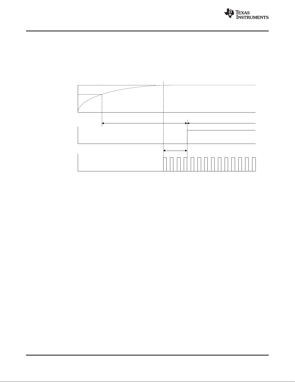
Internal Reset
I2S Clocks
SCK, BCK, LRCK
Internal Reset
4 ms
Reset Removal
2.8V
3.3V
AVDD, DVDD,
CPVDD
PCM5100, PCM5101, PCM5102
Draft Only
SLAS764A –MAY 2011–REVISED MARCH 2012
www.ti.com
APPLICATION INFORMATION
Reset and System Clock Functions
Power-On Reset Function
The PCM510x includes a power-on reset function shown in Figure 11. With VDD> 2.8V, the power-on reset
function is enabled. After the initialization period, the PCM510x is set to its default reset state.
Figure 11. Power-On Reset Timing, DVDD = 3.3V
10 Submit Documentation Feedback Copyright © 2011–2012, Texas Instruments Incorporated
Product Folder Link(s): PCM5100 PCM5101 PCM5102
Page 11
t
SCKH
System Clock
(SCK)
t
SCKL
"L"
"H"
0.3*DVDD
0.7*DVDD
t
SCY
Draft Only
PCM5100, PCM5101, PCM5102
www.ti.com
SLAS764A –MAY 2011–REVISED MARCH 2012
System Clock Input
The PCM510x requires a system clock for operating the digital interpolation filters and advanced segment DAC
modulators. The system clock is applied at the SCK input (pin 12) and supports up to 50MHz. The PCM510x has
a system-clock detection circuit that automatically senses the system-clock frequency. Common audio sampling
frequencies of 8kHz, 16kHz, 32kHz - 44.1kHz - 48kHz, 88.2kHz - 96kHz, 176.4kHz -192kHz, and 384kHz with
±4% tolerance are supported. The sampling frequency detector sets the clock for the digital filter, Delta Sigma
Modulator (DSM) and the Negative Charge pump (NCP) automatically. Table 3 shows examples of system clock
frequencies for common audio sampling rates.
SCK rates that are not common to standard audio clocks, between 1MHz and 50MHz, are only supported in
software mode, available only in the PCM512x and PCM514x devices, by configuring various PLL and clockdivider registers. This allows the device to become a clock master and drive the host serial port with LRCK and
BCK, from a non-audio related clock (e.g. using 12MHz to generate 44.1kHz (LRCK) and 2.8224MHz (BCK) ).
Figure 12 shows the timing requirements for the system clock input. For optimal performance, it is important to
use a clock source with low phase jitter and noise.
Table 3. System Master Clock Inputs for Audio Related Clocks
Sampling
Frequency
8 kHz –
16 kHz –
32 kHz –
44.1 kHz –
48 kHz –
88.2 kHz –
96 kHz –
176.4 kHz –
192 kHz –
64 f
128 f
S
(1)
(1)
(1)
(1)
(1)
(1)
(1)
(1)
(1)
S
(2)
1.0240
(2)
2.0480
(2)
4.0960
(2)
5.6488
(2)
6.1440
(2)
11.2896
(2)
12.2880
22.5792 33.8688 45.1584 –
24.5760 36.8640 49.1520 –
384 kHz 24.5760 49.1520 –
192 f
1.5360
3.0720
6.1440
8.4672
9.2160
256 f
S
(2)
2.0480 3.0720 4.0960 6.1440 8.1920 9.2160 12.2880 16.3840 24.5760
(2)
4.0960 6.1440 8.1920 12.2880 16.3840 18.4320 24.5760 36.8640 49.1520
(2)
8.1920 12.2880 16.3840 24.5760 32.7680 36.8640 49.1520 –
(2)
11.2896 16.9344 22.5792 33.8688 45.1584 –
(2)
12.2880 18.4320 24.5760 36.8640 49.1520 –
16.9344 22.5792 33.8688 45.1584 –
18.4320 24.5760 36.8640 49.1520 –
(1)
(1)
–
System Clock Frequency (f
384 f
S
S
(1)
(1)
(1)
–
512 f
–
–
–
S
(1)
(1)
(1)
(1) This system clock rate is not supported for the given sampling frequency.
(2) This system clock rate is supported by PLL mode.
768 f
–
–
–
) (MHz)
SCK
1024 fS1152 fS1536 fS2048 fS3072 f
S
(1)
(1)
(1)
(1)
(1)
(1)
(1)
(1)
–
(1)
–
(1)
–
(1)
–
(1)
–
(1)
–
(1)
–
(1)
–
(1)
–
(1)
–
(1)
–
(1)
–
(1)
–
(1)
–
(1)
–
(1)
–
(1)
–
S
(1)
(1)
–
(1)
–
(1)
–
(1)
–
(1)
–
(1)
–
(1)
–
(1)
–
(1)
–
(1)
–
(1)
–
(1)
–
(1)
–
(1)
–
(1)
–
Figure 12. Timing Requirements for SCK Input
Table 4. Timing Requirements for SCK Input
Parameters Min Max Unit
t
SCY
t
SCKH
t
SCKL
Copyright © 2011–2012, Texas Instruments Incorporated Submit Documentation Feedback 11
System clock pulse cycle time 20 1000 ns
System clock pulse width, High 9 ns
System clock pulse width, Low 9 ns
Product Folder Link(s): PCM5100 PCM5101 PCM5102
Page 12

PCM5100, PCM5101, PCM5102
Draft Only
SLAS764A –MAY 2011–REVISED MARCH 2012
www.ti.com
System Clock PLL Mode
The system clock PLL mode allows designers to use a simple 3-wire I2S audio source when driving the DAC.
This reduces the need for a high frequency SCK, making PCB layout easier, and reduces high frequency
electromagnetic interference.
The device starts up expecting an external SCK input, but if BCK and LRCK start correctly while SCK remains at
ground level for 16 successive LRCK periods, then the internal PLL will start, automatically generating an internal
SCK from the BCK reference. In the PCM510x, the internal PLL is disabled when an external SCK is supplied;
specific BCK rates are required to generate an appropriate master clock. describes the minimum and maximum
BCK per LRCK for the integrated PLL to automatically generate an internal SCK.
Table 5. BCK Rates (MHz) by LRCK Sample Rate for
PCM510x PLL Operation
BCK (fS)
Sample f (kHz) 32 64
8 - 16 - 1.024
32 1.024 2.048
44.1 1.4112 2.8224
48 1.536 3.072
96 3.072 6.144
192 6.144 12.288
384 12.288 24.576
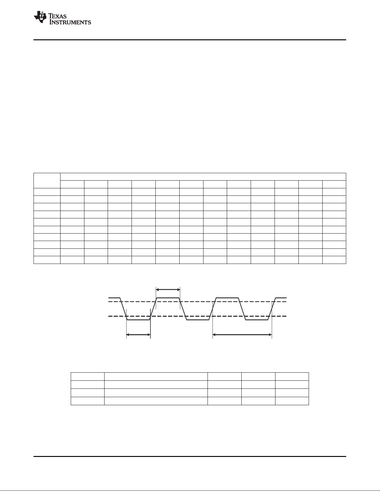
Audio Data Interface
Audio Serial Interface
The audio interface port is a 3-wire serial port. It includes LRCK (pin 15), BCK (pin 13), and DIN (pin 14). BCK is
the serial audio bit clock, and it is used to clock the serial data present on DIN into the serial shift register of the
audio interface. Serial data is clocked into the PCM510x on the rising edge of BCK. LRCK is the serial audio
left/right word clock.
Table 6. PCM510x Audio Data Formats, Bit Depths and Clock Rates
CONTROL MODE FORMAT DATA BITS SCK RATE [x fS] BCK RATE [x fS]
Hardware Control I2S/LJ 32, 24, 20, 16
The PCM510x requires the synchronization of LRCK and system clock, but does not need a specific phase
relation between LRCK and system clock.
If the relationship between LRCK and system clock changes more than ±5 SCK, internal operation is initialized
within one sample period and analog outputs are forced to the bipolar zero level until resynchronization between
LRCK and system clock is completed.
If the relationship between LRCK and BCK are invalid more than 4 LRCK periods, internal operation is initialized
within one sample period and analog outputs are forced to the bipolar zero level until resynchronization between
LRCK and BCK is completed.
MAX LRCK
FREQUENCY [fS]
Up to 192kHz 64, 48, 32
384kHz 64, 128 64, 48, 32
128 – 3072
(≤50MHz)
12 Submit Documentation Feedback Copyright © 2011–2012, Texas Instruments Incorporated
Product Folder Link(s): PCM5100 PCM5101 PCM5102
Page 13

BCK
t
BCH
t
BCL
t
BCY
t
DS
t
DH
t
BL
t
LB
DATA
LRCK
0.5 * DVDD
0.5 * DVDD
0.5 * DVDD
(Input)
(Input)
(Input)
Draft Only
PCM5100, PCM5101, PCM5102
www.ti.com
SLAS764A –MAY 2011–REVISED MARCH 2012
PCM Audio Data Formats and Timing
The PCM510x supports industry-standard audio data formats, including standard I2S and left-justified. Data
formats are selected using the FMT (pin 16), Low for I2S, and High for Left-justified.
All formats require binary 2s complement, MSB-first audio data. Figure 13 shows a detailed timing diagram for
the serial audio interface.
Figure 13. PCM510x Serial Audio Timing - Slave
Table 7. Audio Interface Slave Timing
Parameters Min Max Units
t
BCK Pulse Cycle Time 40 ns
BCY
t
BCK Pulse Width LOW 16 ns
BCL
t
BCK Pulse Width HIGH 16 ns
BCH
t
BCK Rising Edge to LRCK Edge 8 ns
BL
t
LRCK Edge to BCK Rising Edge 8 ns
LB
t
DATA Set Up Time 8 ns
DS
t
DATA Hold Time 8 ns
DH
f
BCK frequency @ DVDD=3.3V 24.576 MHz
BCK
Copyright © 2011–2012, Texas Instruments Incorporated Submit Documentation Feedback 13
Product Folder Link(s): PCM5100 PCM5101 PCM5102
Page 14

LRCK
LSB
L-channel
R-channel
BCK
DATA
MSB LSB
MSB LSB
161521 161521
- ,
DATA
MSB LSB MSB
21 24
2
21 2423
DATA
MSB LSB
MSB LSB
21 3231 21 3231
1/f
S
Audio data word = 16-bit, BCK = 32, 48, 64f
S
Audio data word = 24-bit, BCK = 48, 64f
S
Audio data word = 32-bit, BCK = 64f
S
DATA
LRCK
1/f
S
L- channel R- channel
MSB LSB MSB LSB
DATA
MSB LSB MSB LSB
Audio data word = 16-bit, BCK = 32, 48, 64f
S
DATA
MSB LSB MSB LSB
BCK
161521 161521
2423
2 242321
323121 323121
1
Audio data word = 24-bit, BCK = 48, 64f
S
Audio data word = 32-bit, BCK = 64f
S
PCM5100, PCM5101, PCM5102
Draft Only
SLAS764A –MAY 2011–REVISED MARCH 2012
www.ti.com
Left Justified Data Format; L-channel = HIGH, R-channel = LOW
Figure 14. Left Justified Audio Data Format
I2S Data Format; L-channel = LOW, R-channel = HIGH
14 Submit Documentation Feedback Copyright © 2011–2012, Texas Instruments Incorporated
Figure 15. I2S Audio Data Format
Product Folder Link(s): PCM5100 PCM5101 PCM5102
Page 15
−120
−100
−80
−60
−40
−20
0
0 1 2 3 4
Frequency (x fS)
Amplitude (dB)
G012
−0.4
−0.2
0.0
0.2
0.4
0.6
0.8
1.0
0 50 100 150 200 250 300 350 400
Samples
Amplitude (FFS)
G023
Draft Only
PCM5100, PCM5101, PCM5102
www.ti.com
SLAS764A –MAY 2011–REVISED MARCH 2012
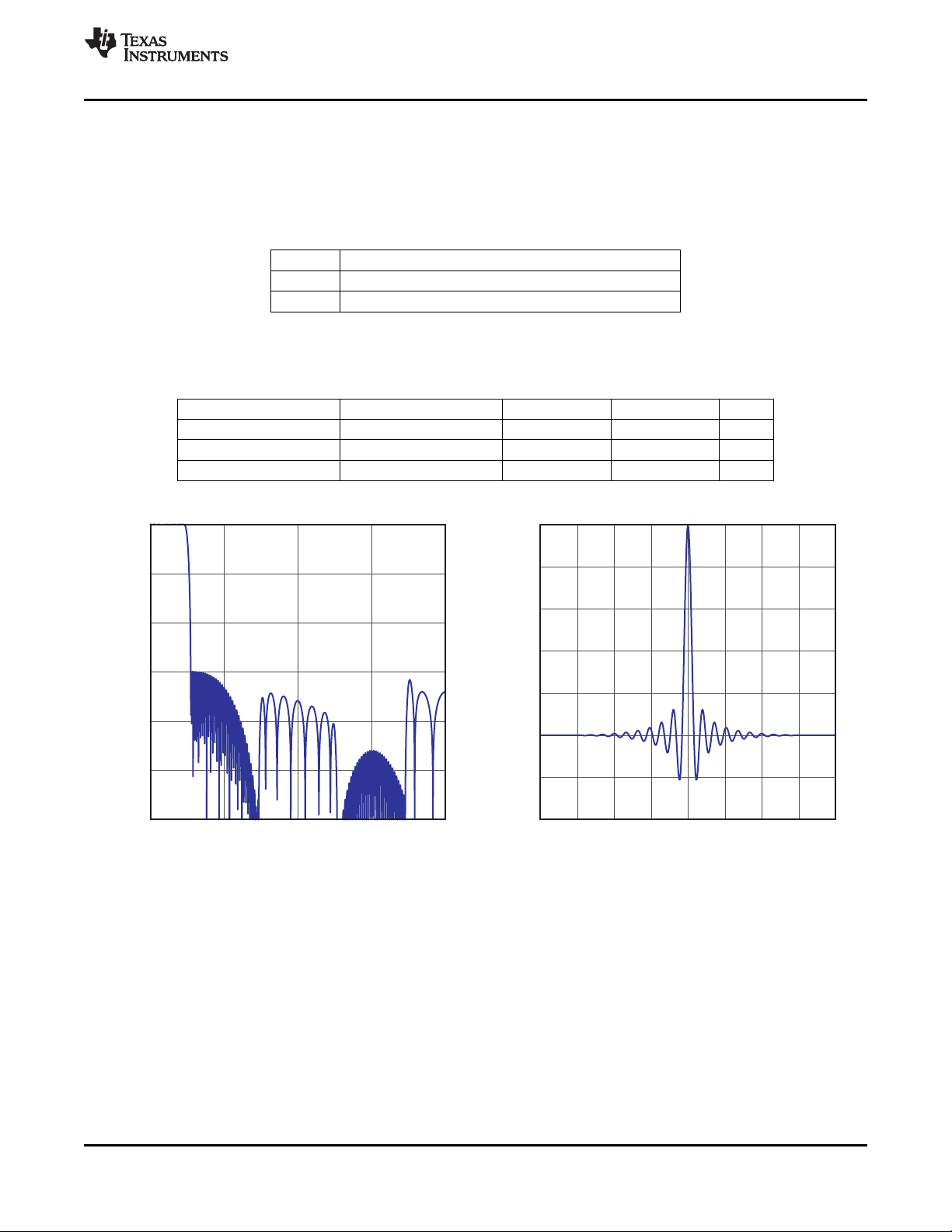
Function Descriptions
Interpolation Filter
The PCM510x provides 2 types of interpolation filter. Users can select which filter to use by using the FLT pin
(pin11)
Table 8. Digital Interpolation Filter Options
FLT Pin Description
0 FIR Normal x8/x4/x2/x1 Interpolation Filters
1 IIR Low Latency x8/x4/x2/x1 Interpolation Filters
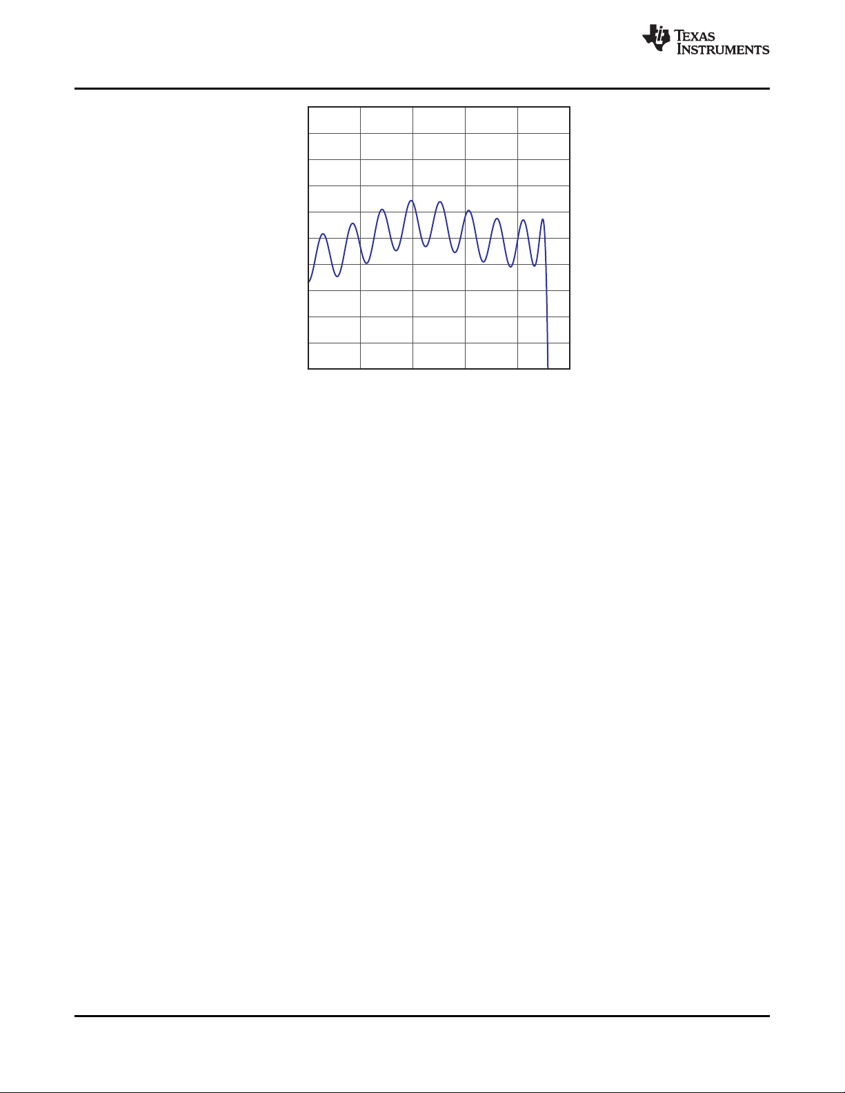
The Normal x8/x4/x2/x1(bypass) Interpolation filter is programmed in 256 cycles in 1 sampling frequency (fS) for
from 8kHz to 384kHz.
Table 9. Normal x8 Interpolation Filter
Parameter Condition Value (Typ) Value (Max) Units
space
Filter Gain Pass Band 0 ……. 0.45f
Filter Gain Stop Band 0.55fS….. 7.455f
S
S
–60 dB
Filter Group Delay 22/f
S
±0.02 dB
s
Figure 16. Normal x8 Interpolation Filter Frequency Figure 17. Normal x8 Interpolation Filter Impulse
Copyright © 2011–2012, Texas Instruments Incorporated Submit Documentation Feedback 15
Response Response
Product Folder Link(s): PCM5100 PCM5101 PCM5102
Page 16
−0.05
−0.04
−0.03
−0.02
−0.01
0.00
0.01
0.02
0.03
0.04
0.05
0.0 0.1 0.2 0.3 0.4 0.5
Frequency (x fS)
Amplitude (dB)
G034
PCM5100, PCM5101, PCM5102
Draft Only
SLAS764A –MAY 2011–REVISED MARCH 2012
Figure 18. Normal x8 Interpolation Filter Passband Ripple
www.ti.com
16 Submit Documentation Feedback Copyright © 2011–2012, Texas Instruments Incorporated
Product Folder Link(s): PCM5100 PCM5101 PCM5102
Page 17

−120
−100
−80
−60
−40
−20
0
0 1 2 3 4
Frequency (x fS)
Amplitude (dB)
G009
−0.4
−0.2
0.0
0.2
0.4
0.6
0.8
1.0
0 20 40 60 80 100 120 140 160
Samples
Amplitude (FFS)
G020
−0.05
−0.04
−0.03
−0.02
−0.01
0.00
0.01
0.02
0.03
0.04
0.05
0.0 0.5 1.0
Frequency (x fS)
Amplitude (dB)
G031
Draft Only
PCM5100, PCM5101, PCM5102
www.ti.com
SLAS764A –MAY 2011–REVISED MARCH 2012
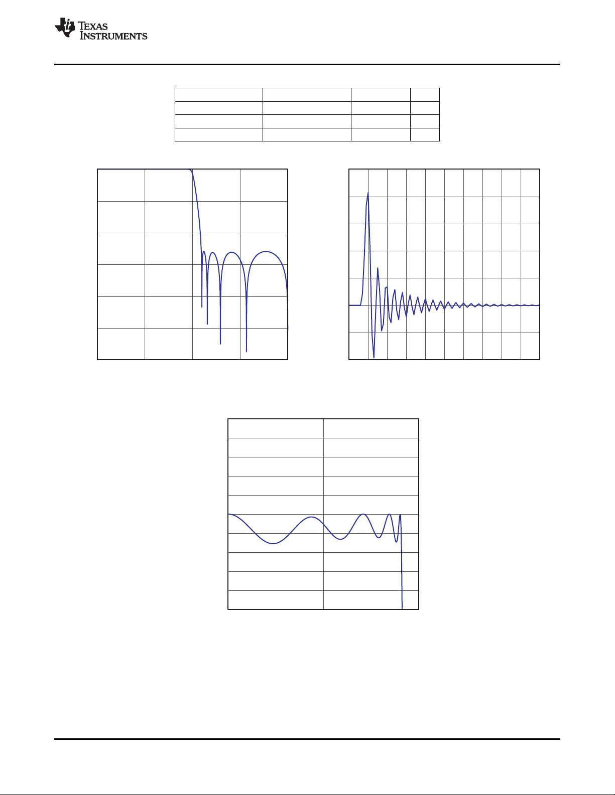
The Normal x4/x2/x1(bypass) Interpolation filter is programmed in 256 cycles in 1 sampling frequency (fS) for
from 8kHz to 384kHz.
Table 10. Normal x4 Interpolation Filter
Parameter Condition Value (Typ) Value (Max) Units
Filter Gain Pass Band 0 ……. 0.45f
Filter Gain Stop Band 0.55fS….. 7.455f
S
S
–60 dB
Filter Group Delay 22/f
S
±0.02 dB
s
space
Figure 19. Normal x4 Interpolation Filter Frequency Figure 20. Normal x4 Interpolation Filter Impulse
Response Response
Copyright © 2011–2012, Texas Instruments Incorporated Submit Documentation Feedback 17
Figure 21. Normal x4 Interpolation Filter Passband Ripple
Product Folder Link(s): PCM5100 PCM5101 PCM5102
Page 18
−120
−100
−80
−60
−40
−20
0
0 1 2 3 4
Frequency (x fS)
Amplitude (dB)
G006
−0.4
−0.2
0.0
0.2
0.4
0.6
0.8
1.0
0 10 20 30 40 50 60 70 80 90 100
Samples
Amplitude (FFS)
G017
−0.05
−0.04
−0.03
−0.02
−0.01
0.00
0.01
0.02
0.03
0.04
0.05
0.0 0.5 1.0 1.5 2.0
Frequency (x fS)
Amplitude (dB)
G028
PCM5100, PCM5101, PCM5102
Draft Only
SLAS764A –MAY 2011–REVISED MARCH 2012
www.ti.com
Normal x2 / x1(bypass) Interpolation filter is programmed in 256 cycles in 1 sampling frequency (fS) for from
8kHz to 384kHz.
Table 11. Normal x2 Interpolation Filter
Parameter Condition Value (Typ) Value (Max) Units
Filter Gain Pass Band 0 ……. 0.45f
Filter Gain Stop Band 0.55fS….. 7.455f
S
S
–60 dB
Filter Group Delay 22/f
S
±0.02 dB
s
space
Figure 22. Normal x2 Interpolation Filter Frequency Figure 23. Normal x2 Interpolation Filter Impulse
Response Response
18 Submit Documentation Feedback Copyright © 2011–2012, Texas Instruments Incorporated
Figure 24. Normal x2 Interpolation Filter Passband Ripple
Product Folder Link(s): PCM5100 PCM5101 PCM5102
Page 19

−120
−100
−80
−60
−40
−20
0
0 1 2 3 4
Frequency (x fS)
Amplitude (dB)
G011
−0.6
−0.4
−0.2
0.0
0.2
0.4
0.6
0.8
1.0
0 50 100 150 200 250 300 350 400
Samples
Amplitude (FFS)
G022
−0.00010
−0.00008
−0.00006
−0.00004
−0.00002
0.00000
0.00002
0.00004
0.00006
0.00008
0.00010
0.0 0.1 0.2 0.3 0.4 0.5
Frequency (x fS)
Amplitude (dB)
G033
Draft Only
PCM5100, PCM5101, PCM5102
www.ti.com
SLAS764A –MAY 2011–REVISED MARCH 2012
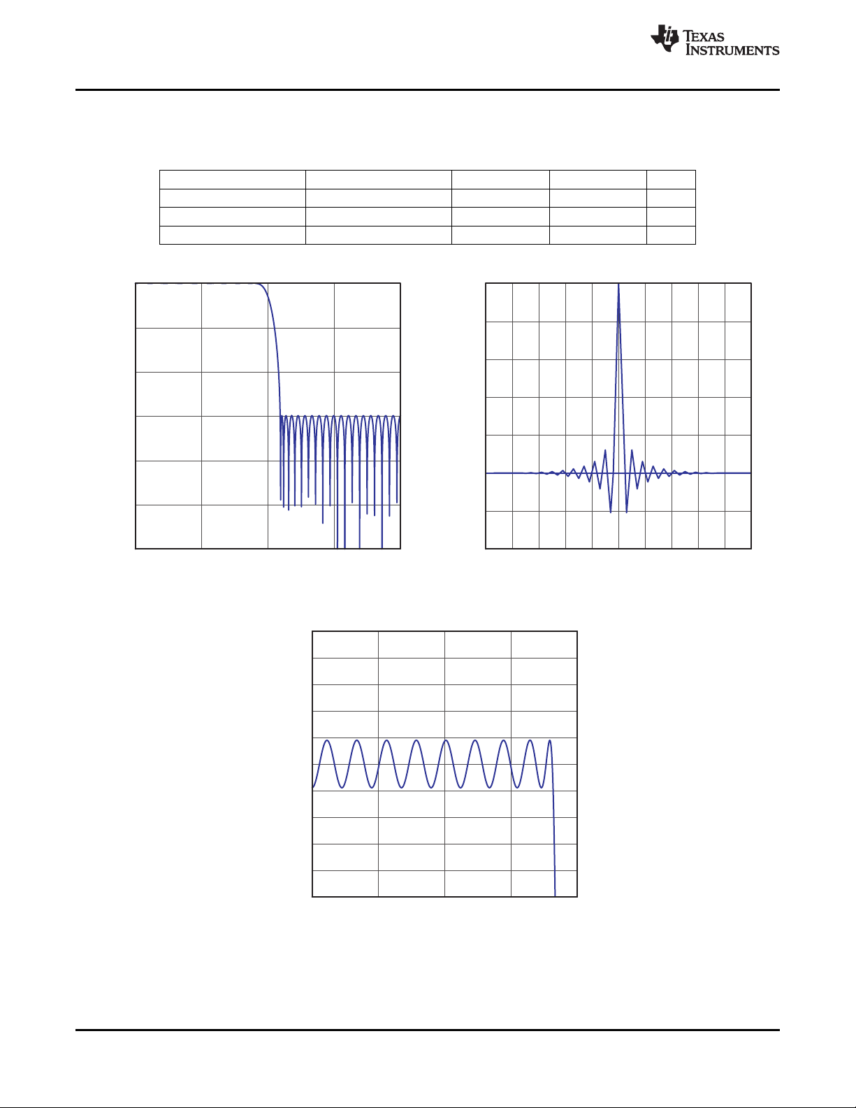
The low-latency x8 / x4 / x2 / x1(bypass) Interpolation filter is programmed in 256 cycles in 1fSfor from 8kHz to
384kHz.
Table 12. Low latency x8 Interpolation Filter
Parameter Condition Value (Typ) Units
Filter Gain Pass Band 0 ……. 0.45f
Filter Gain Stop Band 0.55fS….. 7.455f
S
S
Filter Group Delay 3.5/f
±0.0001 dB
–52 dB
S
s
space
Figure 25. Low latency x8 Interpolation Filter Figure 26. Low latency x8 Interpolation Filter
Frequency Response Impulse Response
Copyright © 2011–2012, Texas Instruments Incorporated Submit Documentation Feedback 19
Figure 27. Low latency x8 Interpolation Filter Passband Ripple
Product Folder Link(s): PCM5100 PCM5101 PCM5102
Page 20

−120
−100
−80
−60
−40
−20
0
0 1 2 3 4
Frequency (x fS)
Amplitude (dB)
G008
−0.6
−0.4
−0.2
0.0
0.2
0.4
0.6
0.8
1.0
0 20 40 60 80 100 120 140 160 180
Samples
Amplitude (FFS)
G019
−0.0001
−0.00008
−0.00006
−0.00004
−0.00002
0
0.00002
0.00004
0.00006
0.00008
0.0001
0.0 0.5 1.0
Frequency (x fS)
Amplitude (dB)
G030
PCM5100, PCM5101, PCM5102
Draft Only
SLAS764A –MAY 2011–REVISED MARCH 2012
Parameter Condition Value (Typ) Units
Filter Gain Pass Band 0 ……. 0.45f
Filter Gain Stop Band 0.55fS….. 3.455f
Filter Group Delay 3.5 s
space
Table 13. Low latency x4 Interpolation Filter
S
S
±0.0001 dB
www.ti.com
–52 dB
Figure 28. Low latency x4 Interpolation Filter Figure 29. Low latency x4 Interpolation Filter
Frequency Response Impulse Response
Figure 30. Low latency x4 Interpolation Filter Passband Ripple
20 Submit Documentation Feedback Copyright © 2011–2012, Texas Instruments Incorporated
Product Folder Link(s): PCM5100 PCM5101 PCM5102
Page 21
−120
−100
−80
−60
−40
−20
0
0 1 2 3 4
Frequency (x fS)
Amplitude (dB)
G005
−0.4
−0.2
0.0
0.2
0.4
0.6
0.8
1.0
0 10 20 30 40 50 60 70 80 90 100
Samples
Amplitude (FFS)
G016
−0.0001
−0.00008
−0.00006
−0.00004
−0.00002
0
0.00002
0.00004
0.00006
0.00008
0.0001
0.0 0.5 1.0
Frequency (x fS)
Amplitude (dB)
G030
Draft Only
PCM5100, PCM5101, PCM5102
www.ti.com
space
SLAS764A –MAY 2011–REVISED MARCH 2012
Table 14. Low latency x2 Interpolation Filter
Parameter Condition Value (Typ) Units
Filter Gain Pass Band 0 ……. 0.45f
Filter Gain Stop Band 0.55fS….. 1.455f
S
S
Filter Group Delay 3.5 s
±0.0001 dB
–52 dB
Figure 31. Low latency x2 Interpolation Filter Figure 32. Low latency x2 Interpolation Filter
Frequency Response Impulse Response
Copyright © 2011–2012, Texas Instruments Incorporated Submit Documentation Feedback 21
Figure 33. Low latency x2 Interpolation Filter Passband Ripple
Product Folder Link(s): PCM5100 PCM5101 PCM5102
Page 22

XSMT
0.9 * DV
DD
t
R
t
F
<20ns
<20ns
0.1 * DV
DD
PCM5100, PCM5101, PCM5102
Draft Only
SLAS764A –MAY 2011–REVISED MARCH 2012
www.ti.com
Zero Data Detect
The PCM510x has a zero-data detect function. When the device detects continuous zero data, it enters a full
analog mute condition.
The PCM510x counts zero data over 1024LRCKs (21ms @ 48kHz) before setting analog mute.
Power Save Mode
When any kind of clock error (SCK, BCK, and LRCK) or clock halt is detected, the PCM510x enters Stand-by
mode automatically. The current-segment DAC and Line driver are also powered down.
When BCK and LRCK halt to a low level for more than 1 second, the PCM510x enters Power down mode
automatically. Power-down mode includes the negative charge pump and Bias/Reference circuit power-down in
addition to stand-by.
Whenever expected Audio clocks (SCK, BCK, LRCK) are applied to the PCM510x, the device starts its powerup
sequence automatically.
XSMT Pin (Soft Mute / Soft Un-Mute)
For external digital control of the PCM510x, the XSMT pin must be driven by an external digital host with a
specific/minimum rise time (tr) and fall time (tf) for soft mute and soft un-mute. The PCM510x requires tr/tftimes
of less than 20ns. In the majority of applications, this shouldn’t be a problem, however, traces with high
capacitance may have issues.
When the XSMT pin is shifted from high to low (3.3V to 0V), a soft digital attenuation ramp is started. –1dB
attenuation will be applied every 1fSfrom 0dBFS to –∞. This takes 104 sample times.
When the XSMT pin is shifted from low to high (0V to 3.3V), a soft digital “un-mute” is started. 1dB gain steps are
applied every fSfrom –∞ to 0dBFS. This takes 104 sample times.
Figure 34. XSMT Timing for Soft Mute and Soft Un-Mute
Table 15. XSMT Timing Parameters
Parameters Min Max Unit
Rise time (tR) 20 ns
Fall time (tF) 20 ns
22 Submit Documentation Feedback Copyright © 2011–2012, Texas Instruments Incorporated
Product Folder Link(s): PCM5100 PCM5101 PCM5102
Page 23

System
VDD
XSMT
7.25kO
2.75kO
12V
supply
0.9 * DVDD
0.1 * DVDD
2.0 V
1.2 V
XSMT
t
f
Digital Attenuation Followed by Analog Mute
Analog Mute
Draft Only
PCM5100, PCM5101, PCM5102
www.ti.com
SLAS764A –MAY 2011–REVISED MARCH 2012
External Power Sense Undervoltage Protection mode
The XSMT pin can also be used to monitor a system voltage, such as the 24VDC LCD TV backlight, or 12VDC
system supply using a potential divider created with two resistors. (See Figure 35 )
• If the XSMT pin makes a transition from 1 to 0 over 6ms or more, the device will switch into external undervoltage protection mode. In this mode, two trigger levels are used.
• When XSMT pin level reaches 2V, soft mute process begins.
• When XSMT pin level reaches 1.2V, analog mute will engage, regardless of digital audio level, and analog
shut down will begin. (i.e. DAC circuitry will power down etc).
A timing diagram to show this is shown in Figure 36.
NOTE
The XSMT input pins voltage range is from –0.3V to DVDD + 0.3V.The ratio of external
resistors must be considered within this input range. Any increase in power supply (such
as power supply positive noise/ripple) can pull the XSMT pin higher than DVDD+0.3V.
For example, if the PCM510x is monitoring a 12V input, and dividing the voltage by 4, then the voltage at XSMT
during ideal power supply conditions will be 3V. If the voltage spikes any higher than 14.4V, then XSMT will see
a voltage in excess of 3.6V (DVDD+0.3), potentially damaging the device.
Providing the divider is set appropriately, any DC voltage can be monitored.
Figure 35. XSMT in External UVP Mode
Figure 36. XSMT Timing for Undervoltage Protection
Copyright © 2011–2012, Texas Instruments Incorporated Submit Documentation Feedback 23
Product Folder Link(s): PCM5100 PCM5101 PCM5102
Page 24

PCM Audio
Source
PCM5100, PCM5101, PCM5102
Draft Only
SLAS764A –MAY 2011–REVISED MARCH 2012
Typical Application Circuits
Figure 37. PCM510x Standard PCM Audio Operation, 3.3V
www.ti.com
Figure 38. PCM510x PLL Operation
24 Submit Documentation Feedback Copyright © 2011–2012, Texas Instruments Incorporated
Product Folder Link(s): PCM5100 PCM5101 PCM5102
Page 25

PCM510x
OUTL
OUTR
470Ω
2.2nF
LINE
OUT
470Ω
2.2nF
Output voltage is
2 VRMS
With a 10kΩ Load
Draft Only
PCM5100, PCM5101, PCM5102
www.ti.com
SLAS764A –MAY 2011–REVISED MARCH 2012
Recommended Output Filter for the PCM510x
The diagram in Figure 39 shows the recommended output filter for the PCM510x. The new PCM510x next
generation current segment architecture offers excellent out of band noise, making a traditional 20kHz low pass
filter a thing of the past.
The RC settings below offer a –3dB filter point at 153kHz (approx), giving the DAC the ability to reproduce
virtually all frequencies through to it’s maximum sampling rate of 384kHz.
Figure 39. Recommended Output Lowpass Filter for 10kΩ Operation
Copyright © 2011–2012, Texas Instruments Incorporated Submit Documentation Feedback 25
Product Folder Link(s): PCM5100 PCM5101 PCM5102
Page 26

PCM5100, PCM5101, PCM5102
Draft Only
SLAS764A –MAY 2011–REVISED MARCH 2012
www.ti.com
REVISION HISTORY
Changes from Revision Initial Release (May 2011) to Revision A Page
• Changed layout of first two pages ........................................................................................................................................ 1
• Deleted "Device Power Dissipation" row .............................................................................................................................. 2
• Changed "VOUT = -1 dB" to " -1 dBFS" in THD+N .............................................................................................................. 4
• Changed reference to correct footnote ................................................................................................................................. 5
• Changed Updated plot .......................................................................................................................................................... 7
• Changed t
• Removed 48kHz sample rate with PLL-generated clock .................................................................................................... 12
• Added BCK frequency max for convenience ...................................................................................................................... 13
• Added PCM510x application diagram, PLL Operation ....................................................................................................... 24
SCKH
and t
values to 9ns. .............................................................................................................................. 11
SCKL
26 Submit Documentation Feedback Copyright © 2011–2012, Texas Instruments Incorporated
Product Folder Link(s): PCM5100 PCM5101 PCM5102
Page 27

PACKAGE OPTION ADDENDUM
www.ti.com
2-Jan-2012
PACKAGING INFORMATION
Orderable Device
PCM5100PW ACTIVE TSSOP PW 20 70 Green (RoHS
PCM5100PWR ACTIVE TSSOP PW 20 2000 Green (RoHS
PCM5101PW ACTIVE TSSOP PW 20 70 Green (RoHS
PCM5101PWR ACTIVE TSSOP PW 20 2000 Green (RoHS
PCM5102PW ACTIVE TSSOP PW 20 70 Green (RoHS
PCM5102PWR ACTIVE TSSOP PW 20 2000 Green (RoHS
(1)
The marketing status values are defined as follows:
ACTIVE: Product device recommended for new designs.
LIFEBUY: TI has announced that the device will be discontinued, and a lifetime-buy period is in effect.
NRND: Not recommended for new designs. Device is in production to support existing customers, but TI does not recommend using this part in a new design.
PREVIEW: Device has been announced but is not in production. Samples may or may not be available.
OBSOLETE: TI has discontinued the production of the device.
Status
(1)
Package Type Package
Drawing
Pins Package Qty
Eco Plan
& no Sb/Br)
& no Sb/Br)
& no Sb/Br)
& no Sb/Br)
& no Sb/Br)
& no Sb/Br)
(2)
Lead/
Ball Finish
CU NIPDAU Level-1-260C-UNLIM
CU NIPDAU Level-1-260C-UNLIM
CU NIPDAU Level-1-260C-UNLIM
CU NIPDAU Level-1-260C-UNLIM
CU NIPDAU Level-1-260C-UNLIM
CU NIPDAU Level-1-260C-UNLIM
MSL Peak Temp
(3)
Samples
(Requires Login)
(2)
Eco Plan - The planned eco-friendly classification: Pb-Free (RoHS), Pb-Free (RoHS Exempt), or Green (RoHS & no Sb/Br) - please check http://www.ti.com/productcontent for the latest availability
information and additional product content details.
TBD: The Pb-Free/Green conversion plan has not been defined.
Pb-Free (RoHS): TI's terms "Lead-Free" or "Pb-Free" mean semiconductor products that are compatible with the current RoHS requirements for all 6 substances, including the requirement that
lead not exceed 0.1% by weight in homogeneous materials. Where designed to be soldered at high temperatures, TI Pb-Free products are suitable for use in specified lead-free processes.
Pb-Free (RoHS Exempt): This component has a RoHS exemption for either 1) lead-based flip-chip solder bumps used between the die and package, or 2) lead-based die adhesive used between
the die and leadframe. The component is otherwise considered Pb-Free (RoHS compatible) as defined above.
Green (RoHS & no Sb/Br): TI defines "Green" to mean Pb-Free (RoHS compatible), and free of Bromine (Br) and Antimony (Sb) based flame retardants (Br or Sb do not exceed 0.1% by weight
in homogeneous material)
(3)
MSL, Peak Temp. -- The Moisture Sensitivity Level rating according to the JEDEC industry standard classifications, and peak solder temperature.
Important Information and Disclaimer:The information provided on this page represents TI's knowledge and belief as of the date that it is provided. TI bases its knowledge and belief on information
provided by third parties, and makes no representation or warranty as to the accuracy of such information. Efforts are underway to better integrate information from third parties. TI has taken and
continues to take reasonable steps to provide representative and accurate information but may not have conducted destructive testing or chemical analysis on incoming materials and chemicals.
TI and TI suppliers consider certain information to be proprietary, and thus CAS numbers and other limited information may not be available for release.
Addendum-Page 1
Page 28

PACKAGE OPTION ADDENDUM
www.ti.com
In no event shall TI's liability arising out of such information exceed the total purchase price of the TI part(s) at issue in this document sold by TI to Customer on an annual basis.
2-Jan-2012
Addendum-Page 2
Page 29

PACKAGE MATERIALS INFORMATION
www.ti.com 14-Nov-2011
TAPE AND REEL INFORMATION
*All dimensions are nominal
Device Package
PCM5100PWR TSSOP PW 20 2000 330.0 16.4 6.95 7.1 1.6 8.0 16.0 Q1
PCM5101PWR TSSOP PW 20 2000 330.0 16.4 6.95 7.1 1.6 8.0 16.0 Q1
PCM5102PWR TSSOP PW 20 2000 330.0 16.4 6.95 7.1 1.6 8.0 16.0 Q1
Type
Package
Drawing
Pins SPQ Reel
Diameter
(mm)
Reel
Width
W1 (mm)
A0
(mm)B0(mm)K0(mm)P1(mm)W(mm)
Pin1
Quadrant
Pack Materials-Page 1
Page 30

PACKAGE MATERIALS INFORMATION
www.ti.com 14-Nov-2011
*All dimensions are nominal
Device Package Type Package Drawing Pins SPQ Length (mm) Width (mm) Height (mm)
PCM5100PWR TSSOP PW 20 2000 346.0 346.0 33.0
PCM5101PWR TSSOP PW 20 2000 346.0 346.0 33.0
PCM5102PWR TSSOP PW 20 2000 346.0 346.0 33.0
Pack Materials-Page 2
Page 31

Page 32

IMPORTANT NOTICE
Texas Instruments Incorporated and its subsidiaries (TI) reserve the right to make corrections, modifications, enhancements, improvements,
and other changes to its products and services at any time and to discontinue any product or service without notice. Customers should
obtain the latest relevant information before placing orders and should verify that such information is current and complete. All products are
sold subject to TI’s terms and conditions of sale supplied at the time of order acknowledgment.
TI warrants performance of its hardware products to the specifications applicable at the time of sale in accordance with TI’s standard
warranty. Testing and other quality control techniques are used to the extent TI deems necessary to support this warranty. Except where
mandated by government requirements, testing of all parameters of each product is not necessarily performed.
TI assumes no liability for applications assistance or customer product design. Customers are responsible for their products and
applications using TI components. To minimize the risks associated with customer products and applications, customers should provide
adequate design and operating safeguards.
TI does not warrant or represent that any license, either express or implied, is granted under any TI patent right, copyright, mask work right,
or other TI intellectual property right relating to any combination, machine, or process in which TI products or services are used. Information
published by TI regarding third-party products or services does not constitute a license from TI to use such products or services or a
warranty or endorsement thereof. Use of such information may require a license from a third party under the patents or other intellectual
property of the third party, or a license from TI under the patents or other intellectual property of TI.
Reproduction of TI information in TI data books or data sheets is permissible only if reproduction is without alteration and is accompanied
by all associated warranties, conditions, limitations, and notices. Reproduction of this information with alteration is an unfair and deceptive
business practice. TI is not responsible or liable for such altered documentation. Information of third parties may be subject to additional
restrictions.
Resale of TI products or services with statements different from or beyond the parameters stated by TI for that product or service voids all
express and any implied warranties for the associated TI product or service and is an unfair and deceptive business practice. TI is not
responsible or liable for any such statements.
TI products are not authorized for use in safety-critical applications (such as life support) where a failure of the TI product would reasonably
be expected to cause severe personal injury or death, unless officers of the parties have executed an agreement specifically governing
such use. Buyers represent that they have all necessary expertise in the safety and regulatory ramifications of their applications, and
acknowledge and agree that they are solely responsible for all legal, regulatory and safety-related requirements concerning their products
and any use of TI products in such safety-critical applications, notwithstanding any applications-related information or support that may be
provided by TI. Further, Buyers must fully indemnify TI and its representatives against any damages arising out of the use of TI products in
such safety-critical applications.
TI products are neither designed nor intended for use in military/aerospace applications or environments unless the TI products are
specifically designated by TI as military-grade or "enhanced plastic." Only products designated by TI as military-grade meet military
specifications. Buyers acknowledge and agree that any such use of TI products which TI has not designated as military-grade is solely at
the Buyer's risk, and that they are solely responsible for compliance with all legal and regulatory requirements in connection with such use.
TI products are neither designed nor intended for use in automotive applications or environments unless the specific TI products are
designated by TI as compliant with ISO/TS 16949 requirements. Buyers acknowledge and agree that, if they use any non-designated
products in automotive applications, TI will not be responsible for any failure to meet such requirements.
Following are URLs where you can obtain information on other Texas Instruments products and application solutions:
Products Applications
Audio www.ti.com/audio Automotive and Transportation www.ti.com/automotive
Amplifiers amplifier.ti.com Communications and Telecom www.ti.com/communications
Data Converters dataconverter.ti.com Computers and Peripherals www.ti.com/computers
DLP® Products www.dlp.com Consumer Electronics www.ti.com/consumer-apps
DSP dsp.ti.com Energy and Lighting www.ti.com/energy
Clocks and Timers www.ti.com/clocks Industrial www.ti.com/industrial
Interface interface.ti.com Medical www.ti.com/medical
Logic logic.ti.com Security www.ti.com/security
Power Mgmt power.ti.com Space, Avionics and Defense www.ti.com/space-avionics-defense
Microcontrollers microcontroller.ti.com Video and Imaging www.ti.com/video
RFID www.ti-rfid.com
OMAP Mobile Processors www.ti.com/omap
Wireless Connectivity www.ti.com/wirelessconnectivity
TI E2E Community Home Page e2e.ti.com
Mailing Address: Texas Instruments, Post Office Box 655303, Dallas, Texas 75265
Copyright © 2012, Texas Instruments Incorporated
 Loading...