

SBAS327A − JUNE 2004 − REVISED SEPTEMBER 2004
Please be aware that an important notice concerning availability, standard warranty, and use in critical applications of Texas Instruments
!"#
$%
FEATURES
D Four High-Performance Delta-Sigma
Analog-to-Digital Converters
− 24-Bit Linear PCM or 1-Bit Direct Stream
Digital (DSD) Output Data
− Supports PCM Output Sampling Rates up
to 216kHz
− Supports 64fS and 128fS DSD Output Data
Rates
D Dynamic Performance: PCM Output
− Dynamic Range: 118dB
− THD+N: −105dB
D Dynamic Performance: DSD Output
− Dynamic Range: 115dB
− THD+N: −103dB
D Audio Serial Port
− 24-Bit Linear PCM Output Data
− Master or Slave Mode Operation
− Supports Left-Justified, Right-Justified,
I2S, and TDM Data Formats
D DSD Data Port
− Supports DSD Output or Input for All Four
Channels Simultaneously
− Input Mode Provides 1-Bit DSD to 24-Bit
PCM Data Format Conversion
D Additional PCM Output Features
− Linear-Phase Digital Decimation Filter
− Digital High-Pass Filter for DC Removal
− Clipping Flag Output for Each Channel
D Power Supplies: +5V Analog and +3.3V Digital
D Power Dissipation:
− fS = 48kHz: 600mW typical
− fS = 96kHz: 640mW typical
− fS = 192kHz: 615mW typical
D Power-Down Mode
D Available in a Thermally-Enhanced HTQFP-64
Package
APPLICATIONS
D Digital Recorders and Mixing Desks
D Digital Audio Effects Processors
D Broadcast Studio Equipment
D Surround Sound Encoders
D High-End A/V Receivers
DESCRIPTION
The PCM4204 is a high-performance, four-channel
analog-to-digital (A/D) converter designed for professional
and broadcast audio applications. The PCM4204
architecture utilizes a 1-bit delta-sigma modulator per
channel incorporating a novel density modulated dither
scheme for improved dynamic performance.
The PCM4204 supports 24-bit linear PCM output data,
with sampling frequencies up to 216kHz. The PCM4204
can also be configured to output either 64x or 128x
oversampled, 1-bit direct stream digital (DSD) data for
each channel. In addition, the PCM4204 supports a DSD
input mode, allowing 1-bit DSD to 24-bit PCM data format
conversion utilizing the on-chip digital decimation filter.
These features make the PCM4204 suitable for a variety
of digital audio recording and processing applications.
The PCM4204 includes a flexible audio serial port interface, which supports standard PCM audio data formats, as
well as time division multiplexed (TDM) PCM data formats.
Multiple format support allows the system designer to
choose the interface format that best suits the end application. Audio data format selection, sampling mode configuration, and high-pass filter functions are all programmed
using dedicated control pins.
The PCM4204 operates from a +5V analog power
supply and a +3.3V digital power supply. The digital I/O
pins are compatible with +3.3V logic families. The
PCM4204 is available in a thermally-enhanced HTQFP-64
PowerPAD package.
semiconductor products and disclaimers thereto appears at the end of this data sheet.
PowerPAD is a registered trademark of Texas Instruments. All other trademarks are the property of their respective owners.
&'!()*'+ !) , , - . ,
,, , )/, *,, , 01.
,, , ,,1 , ,.
www.ti.com
Copyright 2004, Texas Instruments Incorporated
$%
Supply voltage
www.ti.com
SBAS327A − JUNE 2004 − REVISED SEPTEMBER 2004
This integrated circuit can be damaged by ESD. Texas Instruments recommends that all integrated circuits be handled with appropriate
precautions. Failure to observe proper handling and installation procedures can cause damage.
ESD damage can range from subtle performance degradation to complete device failure. Precision integrated circuits may be more susceptible to
damage because very small parametric changes could cause the device not to meet its published specifications.
ABSOLUTE MAXIMUM RATINGS
over operat i n g f ree-air temperature range unless otherwise noted
VCC1, VCC2 +6.0 V
VDD1, VDD2, VDD3 +3.6 V
Ground voltage differences (any AGND to DGND or BGND) ±0.1 V
FMT0, FMT1, FMT2, S/M, FS0, FS1, FS2,
Digital input voltage
Analog input voltage VIN1−4+, VIN1−4− −0.3 to (VCC + 0.3) V
Input current (any pin except supplies) ±10mA V
Operating temperature range −10 to +70 °C
Storage temperature range, T
(1)
Stresses above those listed under Absolute Maximum Ratings may cause permanent damage to the device. Exposure to absolute maximum
conditions for extended periods may degrade device reliability. These are stress ratings only, and functional operation of the device at these or
any other conditions beyond those specified is not implied.
STG
SCKI, RST, HPFD, SUB, BCK, LRCK,
DSDCLK, DSD1, DSD2, DSD3, DSD4, TEST
(1)
PCM4204 UNIT
−0.3 to (VDD + 0.3) V
−65 to +150 °C
PACKAGE/ORDERING INFORMATION
For the most current package and ordering information, see the Package Option Addendum located at the end of this
datasheet.
2
$%
V
V
www.ti.com
SBAS327A − JUNE 2004 − REVISED SEPTEMBER 2004
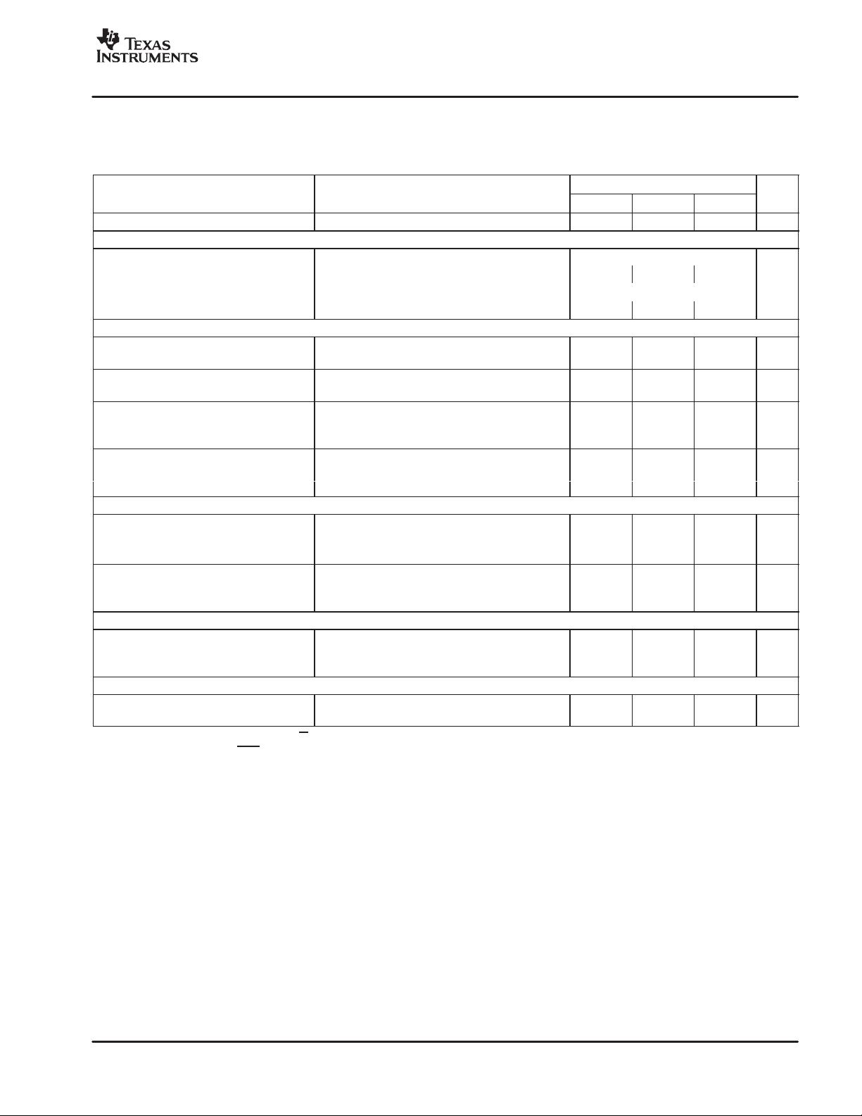
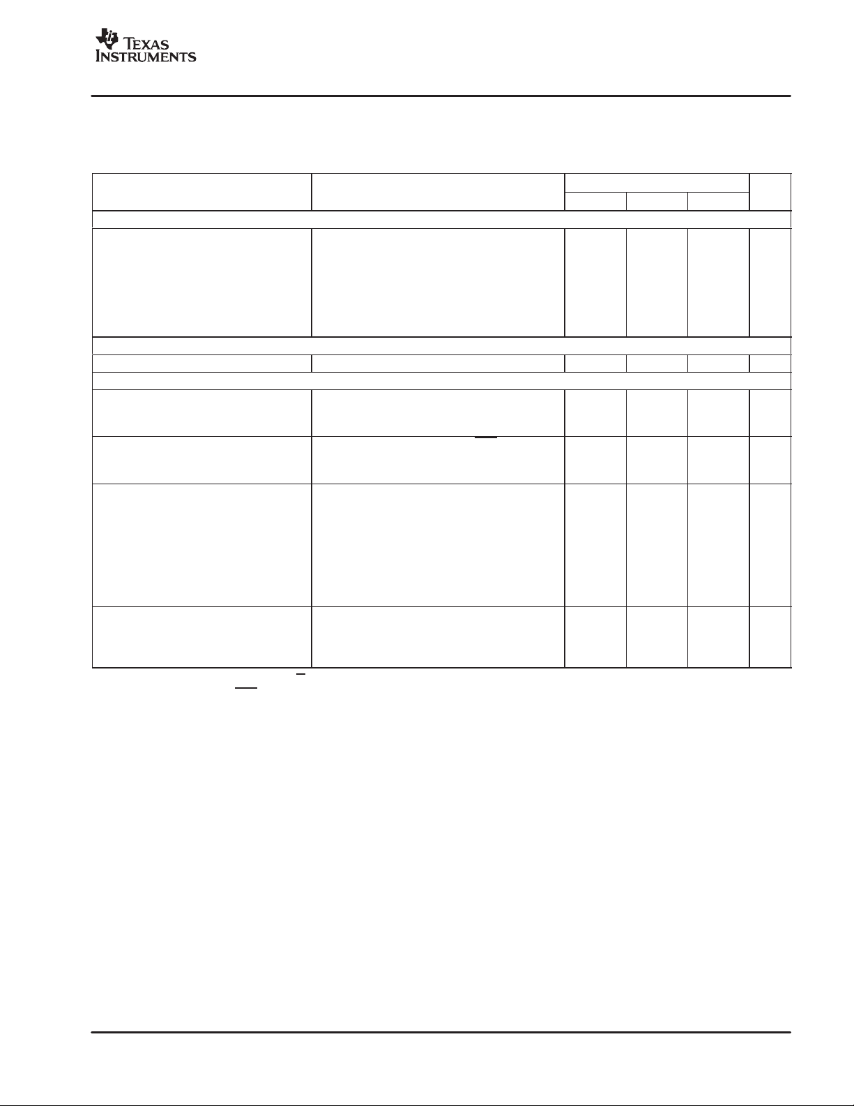
ELECTRICAL CHARACTERISTICS
Unless otherwise noted, all characteristics specified with TA = +25°C, VCC = +5V , VDD = +3.3V , system clock (SCKI) is 512fS for Single Rate
Sampling, 256fS for Dual Rate Sampling, or 128fS for Quad Rate Sampling. The device is operated in Master mode for all dynamic performance
measurements.
PCM4204
PARAMETER TEST CONDITIONS MIN TYP MAX UNIT
RESOLUTION 24 Bits
DATA FORMAT
Audio Data Formats (PCM) Left and Right Justified, I2S, TDM
Audio Data Word Length (PCM) 24 Bits
Binary Data Format (PCM) Two’s Complement Binary, MSB First
DSD Output Format and Word Length 1-Bit Data Bits
DIGIT AL INPUT/OUTPUT
Input Logic Level V
Output Logic Level V
Input Leakage
(1)
Current
Input Leakage
(2)
Current
CLOCK FREQUENCIES
System Clock Frequency, f
Sampling Frequency, f
ANALOG INPUTS
Full Scale Input Voltage Differential Input 6.0 V
Average Input Impedance 3 kΩ
Common-mode Rejection 85 dB
DC SPECIFICATIONS
V
12, V
COM
V
12, V
COM
(1)
Applies to the FMT0, FMT1, FMT2, S/M, FS0, FS1, FS2, HPFD, BCK, LRCK, SUB, DSDCLK, DSD1, DSD2, DSD3, DSD4, and SCKI pins.
(2)
Applies to the TEST and RST pins.
(3)
Typical performance is measured using an Audio Precision System Two Cascade or Cascade Plus test system. The measurement bandwidth
is limited using the Audio Precision 22Hz high-pass filter in combination with either a 20kHz low-pass filter for fS = 48kHz or a 40kHz low-pass
filter for fS = 96kHz and 192kHz. All A-weighted measurements are performed using the A-weighting filter in combination with the band limiting
filters already mentioned. The measurements are made with the RMS detector selected.
(4)
A 256fS system clock is used at final production test for fS = 48kHz measurements.
(5)
Typical DSD performance is measured using an Audio Precision System Two Cascade or Cascade Plus test system. The measurement
bandwidth is limited using the Audio Precision 22Hz high-pass filter in combination with a 20kHz low-pass filter . All A-weighted measurements
are performed using the A-weighting filter in combination with the band limiting filter already mentioned. The measurements are made with the
RMS detector selected. The 1-bit DSD data is converted to 24-bit linear PCM data for measurement using a PCM4204 configured for DSD input
mode.
34 Output Voltage +2.5 V
COM
34 Output Current 200 µA
COM
SCKI
S
IH
V
IL
OH
V
OL
I
IH
I
IL
I
IH
I
IL
IOH = −2mA 0.8 x V
IOH = +2mA 0 0.2 x V
VIN = V
DD
VIN = 0V −1 −10 µA
VIN = V
DD
VIN = 0V −35 −100 µA
Single Rate Sampling Mode 6.144 38.4 MHz
Dual Rate Sampling Mode 12.8 38.4 MHz
Quad Rate Sampling Mode 12.8 38.4 MHz
Single Rate Sampling Mode 24 54 kHz
Dual Rate Sampling Mode 54 108 kHz
Quad Rate Sampling Mode 108 216 kHz
0.7 x V
DD
0 0.3 x V
DD
+1 +10 µA
+35 +100 µA
V
DD
DD
V
DD
DD
PP
3
$%
www.ti.com
SBAS327A − JUNE 2004 − REVISED SEPTEMBER 2004
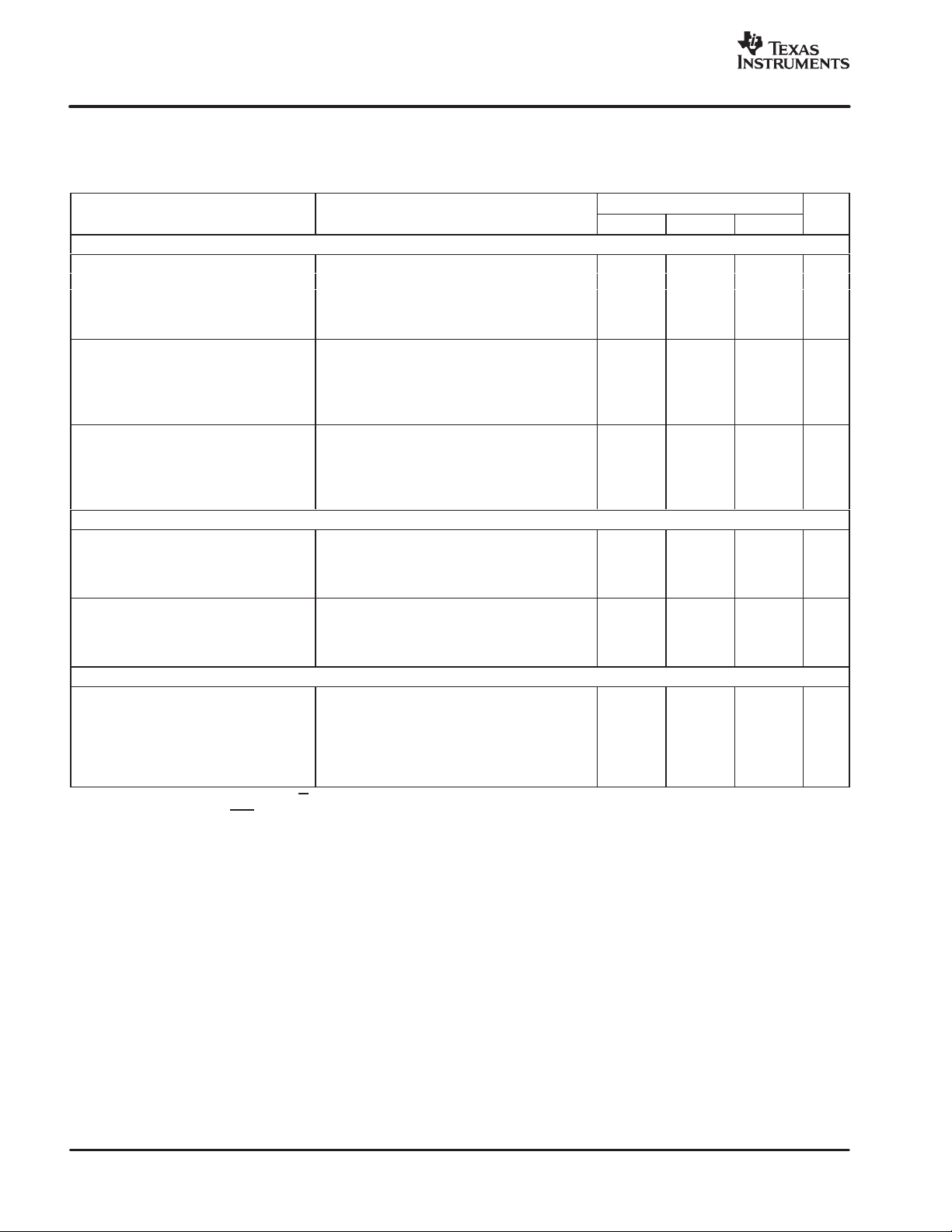
ELECTRICAL CHARACTERISTICS (continued)
Unless otherwise noted, all characteristics specified with TA = +25°C, VCC = +5V , VDD = +3.3V , system clock (SCKI) is 512fS for Single Rate
Sampling, 256fS for Dual Rate Sampling, or 128fS for Quad Rate Sampling. The device is operated in Master mode for all dynamic performance
measurements.
PCM4204
PARAMETER UNITMAXTYPMINTEST CONDITIONS
DYNAMIC PERFORMANCE (PCM Output)
fS = 48kHz
THD+N VIN = −0.5dBFS, fIN = 1kHz −105 −96 dB
Dynamic Range VIN = −60dBFS, fIN = 1kHz, A-weighted 112 118 dB
Channel Separation 105 120 dB
fS = 96kHz
THD+N VIN = −0.5dBFS, fIN = 1kHz, BW = 20Hz to 40kHz −103 dB
Dynamic Range VIN = −60dBFS, fIN = 1kHz, A-weighted 118 dB
Channel Separation 120 dB
fS = 192kHz
THD+N VIN = −0.5dBFS, fIN = 1kHz, BW = 20Hz to 40kHz −103 dB
Dynamic Range VIN = 0V , Unweighted, BW = 20Hz to 40kHz 108 dB
Channel Separation 120 dB
DYNAMIC PERFORMANCE (DSD Output)
64fS Output Rate DSDBCK = 2.8224MHz, BW = 20Hz to 20kHz
THD+N VIN = −0.5dBFS, fIN = 1kHz −103 dB
Dynamic Range VIN = −60dBFS, fIN = 1kHz, A-weighted 115 dB
128fS Output Rate DSDBCK = 5.6448MHz, BW = 20Hz to 20kHz
THD+N VIN = −0.5dBFS, fIN = 1kHz −105 dB
Dynamic Range VIN = −60dBFS, fIN = 1kHz, A-weighted 118 dB
DIGIT AL DECIMATION FIL TER
Single and Dual Rate Sampling Modes
Passband Edge −0.005dB 0.453f
Passband Ripple ±0.005 dB
Stop Band Edge 0.547f
Stop Band Attenuation −100 dB
Group Delay 37/f
(1)
(2)
(3)
(4)
(5)
(4)
Applies to the FMT0, FMT1, FMT2, S/M, FS0, FS1, FS2, HPFD, BCK, LRCK, SUB, DSDCLK, DSD1, DSD2, DSD3, DSD4, and SCKI pins.
Applies to the TEST and RST pins.
Typical performance is measured using an Audio Precision System Two Cascade or Cascade Plus test system. The measurement bandwidth
is limited using the Audio Precision 22Hz high-pass filter in combination with either a 20kHz low-pass filter for fS = 48kHz or a 40kHz low-pass
filter for fS = 96kHz and 192kHz. All A-weighted measurements are performed using the A-weighting filter in combination with the band limiting
filters already mentioned. The measurements are made with the RMS detector selected.
A 256fS system clock is used at final production test for fS = 48kHz measurements.
Typical DSD performance is measured using an Audio Precision System Two Cascade or Cascade Plus test system. The measurement
bandwidth is limited using the Audio Precision 22Hz high-pass filter in combination with a 20kHz low-pass filter . All A-weighted measurements
are performed using the A-weighting filter in combination with the band limiting filter already mentioned. The measurements are made with the
RMS detector selected. The 1-bit DSD data is converted to 24-bit linear PCM data for measurement using a PCM4204 configured for DSD input
mode.
(3)
VIN = −60dBFS, fIN = 1kHz −56 dB
VIN = −60dBFS, fIN = 1kHz, BW = 20Hz to 40kHz −52 dB
VIN = 0V , A-weighted 117 dB
(5)
VIN = −60dBFS, fIN = 1kHz −52 dB
VIN = −60dBFS, fIN = 1kHz −56 dB
S
S
S
Hz
Hz
sec
4
$%
www.ti.com
SBAS327A − JUNE 2004 − REVISED SEPTEMBER 2004
ELECTRICAL CHARACTERISTICS (continued)
Unless otherwise noted, all characteristics specified with TA = +25°C, VCC = +5V , VDD = +3.3V , system clock (SCKI) is 512fS for Single Rate
Sampling, 256fS for Dual Rate Sampling, or 128fS for Quad Rate Sampling. The device is operated in Master mode for all dynamic performance
measurements.
PCM4204
PARAMETER UNITMAXTYPMINTEST CONDITIONS
DIGIT AL DECIMATION FILTER (continued)
Quad Rate Sampling Mode
Passband Edge −0.005dB 0.375f
−3dB 0.490f
Passband Ripple ±0.005 dB
Stop Band Edge 0.770f
Stop Band Attenuation −135 dB
Group Delay 9.5/f
DIGIT AL HIGH PASS FILTER
Frequency Response (−3dB) fS/48000 Hz
POWER SUPPLY
Voltage Range
VCC1, VCC2 +4.75 +5.0 +5.25 VDC
VDD1, VDD2, VDD3 +3.0 +3.3 +3.6 VDC
Power Down Supply Current VCC = +5V , VDD = +3.3V , RST = Low
ICC1 + ICC2 10 mA
IDD1 + IDD2 + IDD3 2 mA
Quiescent Current ICC1 + ICC2 VCC = +5.0V
fS = 48kHz
fS = 96kHz 108 130 mA
fS = 192kHz 108 130 mA
IDD1 + IDD2 + IDD3 VDD = +3.3V
fS = 48kHz
fS = 96kHz 30 44 mA
fS = 192kHz 23 26 mA
Total Power Dissipation VCC = +5V , VDD = +3.3V
fS = 48kHz
fS = 96kHz 640 795 mW
fS = 192kHz 615 736 mW
(1)
Applies to the FMT0, FMT1, FMT2, S/M, FS0, FS1, FS2, HPFD, BCK, LRCK, SUB, DSDCLK, DSD1, DSD2, DSD3, DSD4, and SCKI pins.
(2)
Applies to the TEST and RST pins.
(3)
Typical performance is measured using an Audio Precision System Two Cascade or Cascade Plus test system. The measurement bandwidth
is limited using the Audio Precision 22Hz high-pass filter in combination with either a 20kHz low-pass filter for fS = 48kHz or a 40kHz low-pass
filter for fS = 96kHz and 192kHz. All A-weighted measurements are performed using the A-weighting filter in combination with the band limiting
filters already mentioned. The measurements are made with the RMS detector selected.
(4)
A 256fS system clock is used at final production test for fS = 48kHz measurements.
(5)
Typical DSD performance is measured using an Audio Precision System Two Cascade or Cascade Plus test system. The measurement
bandwidth is limited using the Audio Precision 22Hz high-pass filter in combination with a 20kHz low-pass filter . All A-weighted measurements
are performed using the A-weighting filter in combination with the band limiting filter already mentioned. The measurements are made with the
RMS detector selected. The 1-bit DSD data is converted to 24-bit linear PCM data for measurement using a PCM4204 configured for DSD input
mode.
(4)
(4)
(4)
S
S
108 130 mA
18 23 mA
600 726 mW
Hz
S
Hz
S
Hz
sec
5
$%
SBAS327A − JUNE 2004 − REVISED SEPTEMBER 2004
PIN ASSIGNMENT
www.ti.com
VIN1
V
IN
NC
NC
V
CC
AGND1
BGND1
DGND1
V
DD
RST
TEST
FS0
FS1
FS2
SCKI
BGND2
−
12+
12
REF
V
V
64 63 62 61 60 59 58 57 56 55 54
−
1
2
1+
12
REF
AGND4
COM
V
NC
−
2+
2
IN
IN
V
V
NC
NC
−
3+
3
IN
V
V
34
IN
NC
COM
V
53 52 51 50 49
3
4
5
1
6
7
8
9
1
PCM4204
10
11
12
13
14
15
16
AGND3
−
34
34+
REF
REF
V
V
48
VIN4+
47
−
V
4
IN
46
NC
45
NC
44
2
V
CC
43
AGND2
42
BGND4
41
DGND3
40
V
3
DD
39
SUB
38
HPFD
37
CLIP4
36
CLIP3
35
CLIP2
34
CLIP1
33
BGND3
17 18 19 20 21 22 23 24 25 26 27
DGND2
2
DD
V
DSD1
DSD2
DSDCLK
S/M
FMT0
FMT1
NC
FMT2
28 29 30 31 32
DSD4
BCK
LRCK
DSD3
SDOUT1
SDOUT2
6
www.ti.com
SBAS327A − JUNE 2004 − REVISED SEPTEMBER 2004
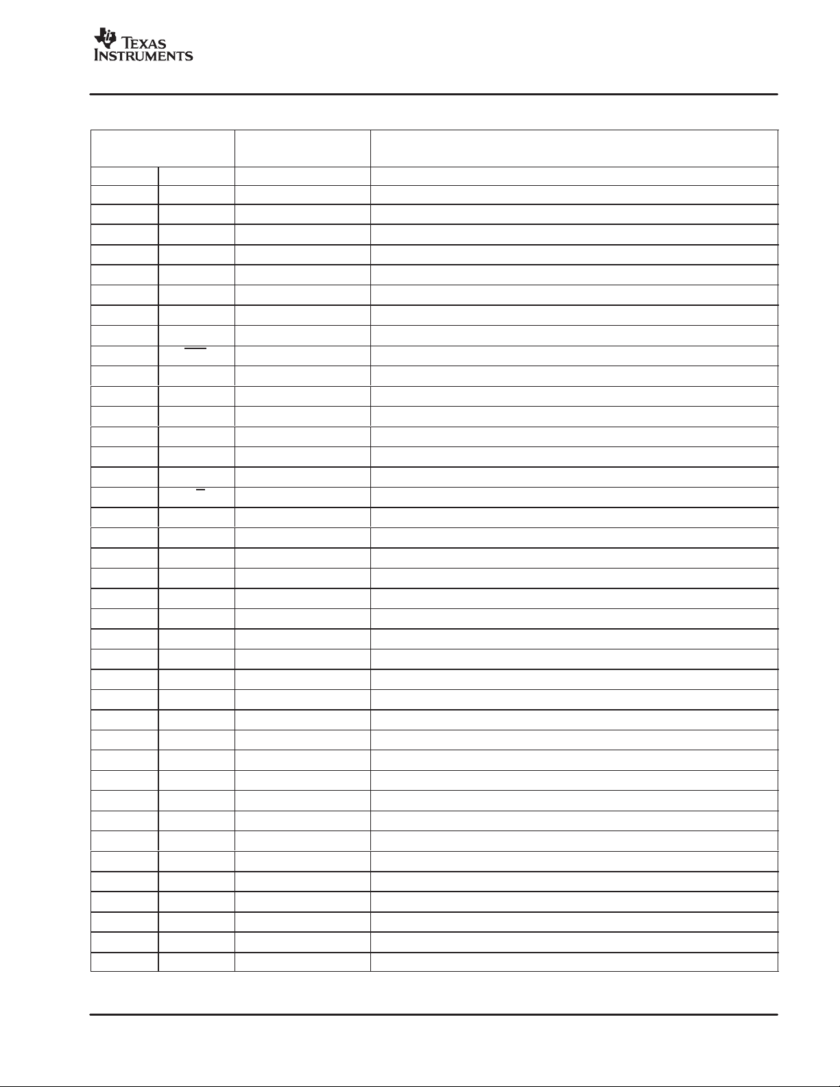
Terminal Functions
TERMINAL
PIN NO. NAME I/O DESCRIPTION
1 VIN1− Input Channel 1 Analog Input, Inverting
2 VIN1+ Input Channel 1 Analog Input, Non-inverting
3 NC — No Internal Connection
4 NC — No Internal Connection
5 VCC1 Power Analog Supply, +5V Nominal
6 AGND1 Ground Analog Ground
7 BGND1 Ground Substrate Ground
8 DGND1 Ground Digital Ground
9 VDD1 Power Digital Supply, +3.3V Nominal
10 RST Input Reset/Power Down (Active Low with internal pull-up to VDD1)
11 TEST Input Test Pin (Active High with internal pull-down to DGND)
12 FS0 Input Sampling Mode
13 FS1 Input Sampling Mode
14 FS2 Input Sampling Mode
15 SCKI Input System Clock
16 BGND2 Ground Substrate Ground
17 S/M Input Audio Serial Port Slave/Master Mode (0 = Master, 1 = Slave)
18 FMT0 Input Audio Data Format
19 FMT1 Input Audio Data Format
20 FMT2 Input Audio Data Format
21 NC — No Internal Connection
22 DGND2 Ground Digital Ground
23 VDD2 Power Digital Supply, +3.3V Nominal
24 DSDCLK I/O DSD Data Clock
25 DSD1 I/O Channel 1 DSD Data
26 DSD2 I/O Channel 2 DSD Data
27 DSD3 I/O Channel 3 DSD Data
28 DSD4 I/O Channel 4 DSD Data
29 BCK I/O Audio Serial Port Bit Clock
30 LRCK I/O Audio Serial Port Left/Right (or Word) Clock
31 SDOUT1 Output PCM Data for Channels 1 and 2
32 SDOUT2 Output PCM Data for Channels 3 and 4
33 BGND3 Ground Substrate Ground
34 CLIP1 Output Channel 1 Clipping Flag (Active High)
35 CLIP2 Output Channel 2 Clipping Flag (Active High)
36 CLIP3 Output Channel 3 Clipping Flag (Active High)
37 CLIP4 Output Channel 4 Clipping Flag (Active High)
38 HPFD Input High-Pass Filter Disable (Active High)
39 SUB Input TDM Sub-Frame Assignment (0 = SF 0, 1 = SF 1)
40 VDD3 Power Digital Supply, +3.3V Nominal
(1)
For TDM formats, SDOUT1 carries data for all four channels, while SDOUT2 is driven low.
(1)
(1)
$%
7
$%
SBAS327A − JUNE 2004 − REVISED SEPTEMBER 2004
Terminal Functions (continued)
TERMINAL
PIN NO. DESCRIPTIONI/ONAME
41 DGND3 Ground Digital Ground
42 BGND4 Ground Substrate Ground
43 AGND2 Ground Analog Ground
44 VCC2 Power Analog Supply, +5V Nominal
45 NC — No Internal Connection
46 NC — No Internal Connection
47 VIN4− Input Channel 4 Analog Input, Inverting
48 VIN4+ Input Channel 4 Analog Input, Non-inverting
49 V
50 V
51 AGND3 Output Analog Ground
52 V
53 NC — No Internal Connection
54 VIN3− Input Channel 3 Analog Input, Inverting
55 VIN3+ Input Channel 3 Analog Input, Non-inverting
56 NC — No Internal Connection
57 NC — No Internal Connection
58 VIN2− Input Channel 2 Analog Input, Inverting
59 VIN2+ Input Channel 2 analog Input, Non-inverting
60 NC — No Internal Connection
61 V
62 AGND4 Ground Analog Ground
63 V
64 V
(1)
For TDM formats, SDOUT1 carries data for all four channels, while SDOUT2 is driven low.
34+ Output Voltage Reference De-Coupling for Channels 3 and 4
REF
34− Output Reference Ground for Channels 3 and 4, connect to AGND
REF
34 Output Common-mode Voltage for Channels 3 and 4, +2.5V Nominal
COM
12 Output Common-mode Voltage for Channels 1 and 2, +2.5V Nominal
COM
12− Output Reference Ground for Channels 1 and 2, connect to AGND
REF
12+ Output Voltage Reference De-Coupling for Channels 1 and 2
REF
www.ti.com
8
www.ti.com
SBAS327A − JUNE 2004 − REVISED SEPTEMBER 2004
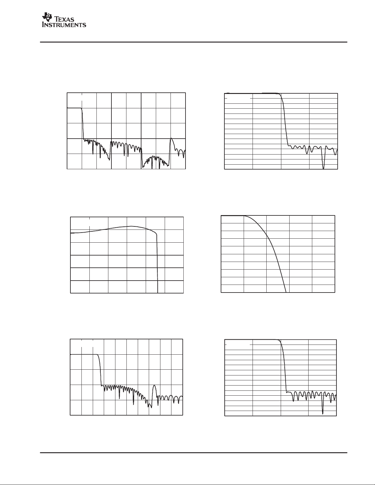
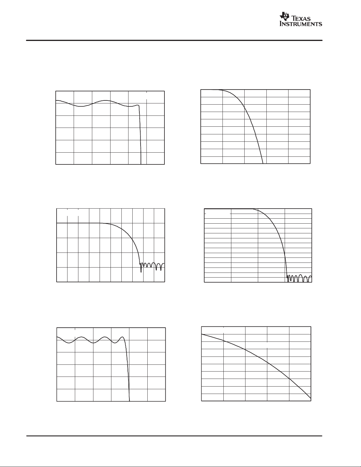
TYPICAL CHARACTERISTICS
At TA = +25°C with VCC = +5V , VDD = +3.3V, and a measurement bandwidth from 20Hz to 20kHz, unless otherwise noted.
$%
OVERALL CHARACTERISTICS
50
SINGLERATE FILTER
fS=48kHz
0
−
50
Amplitude (dB)
−
100
−
150
−
200
0 0.51.01.52.02.53.03.54.0
Normalized Frequency (f
)
S
PASSBAND RIPPLE CHARACTERISTICS
SINGLE RATEFILTER
0.02
fS=48kHz
0
−
0.02
−
0.04
Amplitude (dB)
−
0.06
−
0.08
−
0.1
0
0.1
0.2
0.3
0.4
Normalized Frequency (f
)
S
0.5
0.6
STOP BAND ATTENUATION CHARACTERISTICS
SINGLE RATEFILTER
0
−
10
fS=48kHz
−
20
)
−
30
S
−
40
−
50
−
60
−
70
−
80
−
90
−
100
−
110
−
120
Normalized Frequency (f
−
130
−
140
−
150
0
0.25
Normalized Frequency (f
0.5
S
0.75
)
1
TRANSIENT BAND CHARACTERISTICS
SINGLE RATE FILTER
0
−
1
−
2
−
3
−
4
−
5
−
6
Amplitude (dB)
−
7
−
8
−
9
−
10
=48kHz
f
S
0.510.490.470.45 0.53 0.55
Normalized Frequency (f
)
S
OVERALLCHARACTERISTICS
DUAL RATE FILTER
50
fS= 96kHz
0
−
50
−
100
Amplitude (dB)
−
150
−
Amplitude (dB)
−
−
−
−
−
200
0.2 0.4 0.6 0.8 1.0 1.2 1.4 1.6 1.8 2.00
Normalized Frequency (f
)
S
−
STOP BAND ATTENUATION CHARACTERISTICS
DUAL RATE FILTER
0
−
10
fS=96kHz
−
20
−
30
−
40
−
50
−
60
−
70
−
80
−
90
100
110
120
130
140
150
0
0.25
0.5
Normalized Frequency (f
S
0.75
)
1
9
$%
SBAS327A − JUNE 2004 − REVISED SEPTEMBER 2004
TYPICAL CHARACTERISTICS (continued)
At TA = +25°C with VCC = +5V , VDD = +3.3V, and a measurement bandwidth from 20Hz to 20kHz, unless otherwise noted.
www.ti.com
PASSBAND RIPPLE CHARACTERISTICS
0.02
DUAL RATE FILTER
fS=96kHz
0
−
0.02
−
0.04
Amplitude (dB)
−
0.06
−
0.08
−
0.1
0
0.1
0.2
0.3
0.4
Normalized Frequency(f
0.5
)
S
0.6
0
−
1
−
2
−
3
−
4
−
5
−
6
Amplitude (dB)
−
7
−
8
−
9
−
10
OVERALL CHARACTERISTICS
QUAD RATE FILTER
50
fS= 192kHz
0
−
50
−
100
Amplitude (dB)
−
150
−
200
0.1 0.2 0.3 0.4 0.5 0.6 0.7 0.8 0.9 10
Normalized Frequency (f
)
S
0
−
10
−
20
−
30
−
40
−
50
−
60
−
70
−
80
−
90
−
100
Amplitude (dB)
−
110
−
120
−
130
−
140
−
150
TRANSIENT BAND CHARACTERISTICS
DUAL RATE FILTER
0.510.490.470.45 0.53 0.55
Normalized Frequency (f
)
S
STOP BAND ATTENUATION CHARACTERISTICS
QUAD RATE FILTER
fS= 192kHz
0
0.25
Normalized Frequency (f
0.5
S
0.75
)
= 96kHz
f
S
1
10
PASSBAND RIPPLE CHARACTERISTICS
QUAD RATE FILTER
0.02
fS=192kHz
0
−
0.02
−
0.04
Amplitude (dB)
−
0.06
−
0.08
−
0.1
0
0.1
0.2
0.3
0.4
Normalized Frequency (f
0.5
)
S
0.6
0
−
1
−
2
−
3
−
4
−
5
−
6
Amplitude (dB)
−
7
−
8
−
9
−
10
TRANSIENT BAND CHARACTERISTICS
QUAD RATE FILTER
fS= 192kHz
−
3.90dB at 0.5f
0.510.490.470.45 0.53 0.55
Normalized Frequency (f
S
)
S
www.ti.com
SBAS327A − JUNE 2004 − REVISED SEPTEMBER 2004
TYPICAL CHARACTERISTICS (continued)
At TA = +25°C with VCC = +5V , VDD = +3.3V, and a measurement bandwidth from 20Hz to 20kHz, unless otherwise noted.
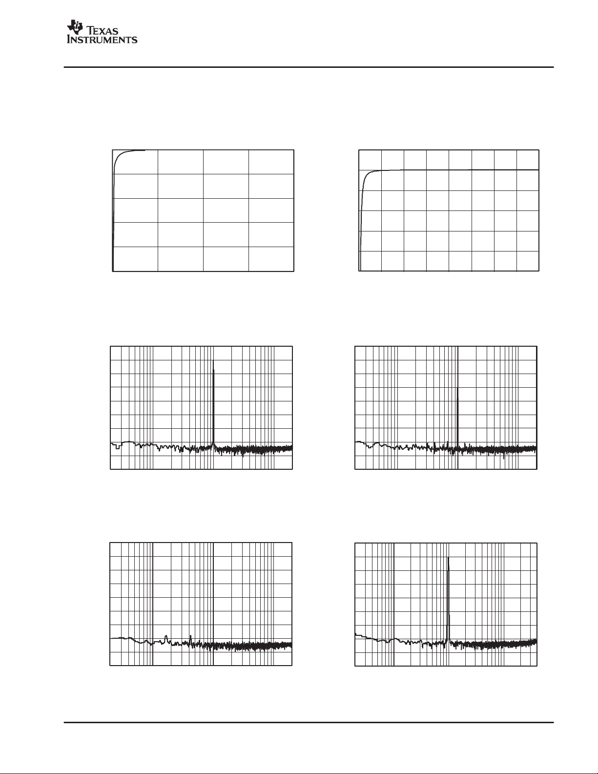
$%
HIGH PASS FILTER
5
−
20
−
40
−
60
Amplitude (dB)
−
80
−
100
0
−
20
−
40
−
60
−
80
−
100
−
120
Amplitude (dB)
−
140
−
160
−
180
STOP BAND CHARACTERISTICS
0.1 0.2 0.3 0.40
Normalized Frequency (f
FFT PLOT
=48kHz,fIN= 997Hz at−20dB)
(f
S
Frequency (Hz)
/1000)
S
1k10020 10k 20k
0.02
0
−
0.02
−
0.04
Amplitude (dB)
−
0.06
−
0.08
−
0.1
00.511.522.533.54
0
−
20
−
40
−
60
−
80
−
100
−
120
Amplitude (dB)
−
140
−
160
−
180
HIGH PASS FILTER
PASSBANDCHARACTERISTICS
Normalized Frequency(f
FFT PLOT
=48kHz,fIN= 997Hz at−60dB)
(f
S
Frequency (Hz)
/1000)
S
1k10020 10k 20k
FFT PLOT
= 48kHz, No Input [Idle])
(f
0
−
20
−
40
−
60
−
80
−
100
−
120
Amplitude (dB)
−
140
−
160
−
180
S
Frequency (Hz)
1k10020 10k 20k
0
−
20
−
40
−
60
−
80
−
100
−
120
Amplitu de (dB)
−
140
−
160
−
180
(f
S
FFT PLOT
=96kHz,fIN= 997Hz at−20dB)
1k10020 10k 40k
Frequency (Hz)
11

$%
SBAS327A − JUNE 2004 − REVISED SEPTEMBER 2004
TYPICAL CHARACTERISTICS (continued)
At TA = +25°C with VCC = +5V , VDD = +3.3V, and a measurement bandwidth from 20Hz to 20kHz, unless otherwise noted.
www.ti.com
FFT PLOT
=96kHz,fIN=997Hzat−60dB)
(f
0
−
20
−
40
−
60
−
80
−
100
−
120
Amplitu de (dB)
−
140
−
160
−
180
0
−
20
−
40
−
60
−
80
−
100
−
120
Amplitu de (dB)
−
140
−
160
−
180
S
1k10020 10k 40k
Frequency (Hz)
FFT PLOT
=192kHz,fIN= 997Hz at−20dB)
(f
S
1k10020 10k 100k
Frequency (Hz)
0
−
20
−
40
−
60
−
80
−
100
−
120
Amplitude (dB)
−
140
−
160
−
180
= 192kHz, fIN=997Hzat−60dB)
(f
0
−
20
−
40
−
60
−
80
−
100
−
120
Amplitude (dB)
−
140
−
160
−
180
S
FFT PLOT
= 96kHz, No Input [Idle])
(f
S
1k10020 10k 40k
Frequency (Hz)
FFT PLOT
1k10020 10k 100k
Frequency (Hz)
12
FFT PLOT
= 192kHz, No Input [Idle])
(f
0
−
20
−
40
−
60
−
80
−
100
−
120
Amplitude (dB)
−
140
−
160
−
180
S
1k10020 10k 100k
Frequency(Hz)
−
90
−
92
−
94
−
96
−
98
−
100
−
102
−
104
−
106
−
108
−
110
−
THD+N (dB)
112
−
114
−
116
−
118
−
120
(f
−
−
140
120−100
THD+N vs AMPLITUDE
=48kHz,fIN= 1kHz, BW = 20Hz to 20kHz)
S
−
80−60
Input Amplitude (dB)
−
40−20 0

www.ti.com
SBAS327A − JUNE 2004 − REVISED SEPTEMBER 2004
TYPICAL CHARACTERISTICS (continued)
At TA = +25°C with VCC = +5V , VDD = +3.3V, and a measurement bandwidth from 20Hz to 20kHz, unless otherwise noted.
THD+N vs FREQUENCY
= 48kHz, Input Amplitude =−1dB,
(f
S
−
90
−
92
−
94
−
96
−
98
−
100
−
102
−
104
−
106
−
108
−
110
THD+N (dB)
−
112
−
114
−
116
−
118
−
120
BW = 20Hz to 20kHz)
1k10020 10k 20k
Input Frequency(Hz)
−
90
−
92
−
94
−
96
−
98
−
100
−
102
−
104
−
106
−
108
−
110
−
THD+N (dB)
112
−
114
−
116
−
118
−
120
(f
−
−
140
120−100
THD+N vs AMPLITUDE
=96kHz,fIN= 1kHz, BW = 20Hz to 4 0kHz)
S
−
80−60
Input Amplitude (dB)
$%
−
40−20 0
THD+N vs FREQUENCY
= 96kHz, InputAmplitude =−1dB,
(f
S
−
70
−
75
−
80
−
85
−
90
−
95
−
100
−
105
THD+N (dB)
−
110
−
115
−
120
BW = 20Hz to 40kHz)
1k10020 10k 40k
Input Frequency (Hz)
−
70
−
75
−
80
−
85
−
90
−
95
−
100
−
105
THD+N (dB)
−
110
−
115
−
120
−
90
−
92
−
94
−
96
−
98
−
100
−
102
−
104
−
106
−
108
−
110
THD+N (dB)
−
112
−
114
−
116
−
118
−
120
THD+N vs FREQUENCY
= 192kHz, Input Amplitude =−1dB,
(f
S
BW = 20Hz to 40kHz)
1k10020 10k 80k
Input Frequency (Hz)
(f
S
−
−
140
120−100
THD+N vs AMPLITUDE
= 192kHz, fIN=1kHz,BW=20Hzto40kHz)
−
80−60
Input Amplitude (dB)
−
40−20 0
13

$%
SBAS327A − JUNE 2004 − REVISED SEPTEMBER 2004
www.ti.com
PRODUCT OVERVIEW
The PCM4204 is a high-performance, four-channel audio
analog-to-digital (A/D) converter designed for use in
professional and broadcast audio applications. The
PCM4204 features 24-bit linear PCM data outputs, as well
as 1-bit Direct Stream Digital (DSD) data output and input
capability for all four channels. Sampling rates up to
216kHz are supported for PCM output formats, while 64x
or 128x oversampled 1-bit data is supported for DSD
modes. Native support for both PCM and DSD data
formats makes the PCM4204 ideal for use in a wide variety
of audio recording and processing applications.
The PCM4204 features 1-bit delta sigma modulators
employing density modulated dither for improved dynamic
performance. Differential voltage inputs are utilized for the
modulators, providing excellent common-mode rejection.
1+
V
IN
VIN1
V
REF
V
REF
AGND4
V
COM
12+
12
12
−
−
Delta−Sigma
Modulator
Reference
DecimationandHighPass
On-chip voltage references are provided for the
modulators, in addition to generating DC common-mode
bias voltage outputs for use with external input circuitry.
Linear phase digital decimation filtering is provided for the
24-bit PCM output, with a minimum stop band attenuation
of −100dB for all sampling modes.
The PCM output mode features clipping flag outputs for
each of the four channels, as well as a digital high-pass
filter for DC removal. The PCM4204 may be configured
using dedicated input pins for sampling mode and audio
data format selection, high-pass filter enable/disable, and
reset/power-down operation.
A +5V power supply is required for the analog section of
the device, while a +3.3V power supply is required for the
digital circuitry. Figure 1 shows the functional block
diagram for the PCM4204.
Digital
Filters
Audio
Serial
Port
DSD
Data
Port
LRCK
BCK
SDOUT1
SDOUT2
DSD1
DSD2
DSD3
DSD4
DSDCLK
V
IN
VIN2
VIN3+
V
V
REF
V
REF
AGND3
V
COM
V
IN
V
IN
34+
34
IN
2+
3
34
4+
4
Delta−Sigma
−
−
−
−
Modulator
Delta−Sigma
Modulator
Reference
Delta−Sigma
Modulator
To/From
Other Blocks
To Other
Blocks
Power and Ground
1
2
CC
CC
V
V
AGND1
AGND2
BGND1
Control
and
Status
System Clock
and
Timing
1
V
BGND2
BGND3
BGND4
2
DGND1
3
DD
DD
V
V
DGND2
DGND3
DD
FS0
FS1
FS2
S/M
FMT0
FMT1
FMT2
HPFD
SUB
RST
CLIP1
CLIP2
CLIP3
CLIP4
SCKI
14
Figure 1. PCM4204 Functional Block Diagram

www.ti.com
SAMPLING FREQUENCY, f
SAMPLING FREQUENCY, f
S
$%
SBAS327A − JUNE 2004 − REVISED SEPTEMBER 2004
ANALOG INPUTS
The PCM4204 includes four channels of A/D conversion,
each with its own pair of dif ferential voltage input pins. The
V
1− (pin 1) and VIN1+ (pin 2) analog inputs correspond
IN
to Channel 1. The V
inputs correspond to Channel 2. The V
V
3+ (pin 55) analog inputs correspond to Channel 3. The
IN
V
4− (pin 47) and VIN4+ (pin 48) analog inputs
IN
2− (pin 58) and VIN2+ (pin 59) analog
IN
3− (pin 54) and
IN
correspond to Channel 4. The average input impedance of
each input pin is 3.0kΩ.
Each analog input pair accepts a full-scale input voltage of
approximately 6.0V
not swing below analog ground or above the V
2 (pin 44) power supplies by more than 300mV.
or V
CC
dif ferential. The analog input should
PP
1 (pin 5)
CC
Schottky diodes may be used to clamp these pins to a safe
input range, or the input buffer circuitry may be designed
in a manner to ensure that the input swing does not exceed
the absolute maximum ratings of the PCM4204.
Refer to
the Applications Information section of this datasheet for
an example input buffer circuit.
VOLTAGE REFERENCES AND COMMON MODE
BIAS VOLTAGE OUTPUTS
The PCM4204 includes two on-chip voltage references,
one for Channels 1 and 2 and another for Channels 3 and
4. The V
12− (pin 63) and V
REF
12+ (pin 64) outputs
REF
correspond to low and high reference outputs for Channels
1 and 2. The V
34− (pin 50) and V
REF
34+ (pin 49)
REF
outputs correspond to low and high reference outputs for
Channels 3 and 4. De-coupling capacitors are connected
between the high and low reference pins, and the low
reference pin is then connected to an analog ground. It is
recommended to have at least a 0.1µF X7R ceramic chip
capacitor connected in parallel with a 33µF low ESR
capacitor (tantalum, multilayer ceramic, or aluminum
electrolytic) for de-coupling purposes.
Refer to the Applications Information section of this
datasheet for the recommended voltage reference pin
connections.
The V
12+ and V
REF
34+ outputs should not be utilized
REF
to bias external circuitry, as they are not buffered. Use the
V
12 (pin 16) and V
COM
external circuitry . Although the V
34 (pin 52) outputs to bias
COM
COM
L and V
COM
R outputs
are internally buffered, the output current is limited to a few
hundred µA. It is recommended to connect these pins to
external nodes with greater than 1MΩ impedance, or to
buffer the outputs with a voltage follower circuit when
driving multiple external nodes.
Refer to the Applications Information section of this
datasheet for an example input buffer circuit that utilizes
the common-mode bias voltage outputs.
SYSTEM CLOCK INPUT
The PCM4204 requires a system clock, from which the
modulator oversampling and digital sub-system clocks ar e
derived. The system clock is applied at the SCKI input (pin
15). The frequency of the system clock is dependent upon
the desired PCM output sampling frequency or DSD data
rate, along with the sampling mode selection. Table 1
shows the corresponding system clock frequencies for
common output sampling and data rates, along with the
corresponding sampling modes. Timing requirements for
the system clock are shown in Figure 2.
SAMPLING MODE
Single Rate 32 n/a n/a 8.192 12.288 16.384 24.576
Single Rate 44.1 n/a n/a 11.2896 16.9344 22.5792 33.8688
Single Rate 48 n/a n/a 12.288 18.432 24.576 36.864
Dual Rate 88.2 n/a n/a 22.5792 33.8688 n/a n/a
Dual Rate 96 n/a n/a 24.576 36.864 n/a n/a
Quad Rate 176.4 22.5792 33.8688 n/a n/a n/a n/a
Quad Rate 192 24.576 36.864 n/a n/a n/a n/a
DSD Input/Output 128fS Data (Single Rate) n/a n/a 11.2896 16.9344 22.5792 33.8688
DSD Input/Output 64fS Data (Dual Rate) n/a n/a 11.2896 16.9344 n/a n/a
Table 1. System Clock Frequencies for Common Output Sampling and Data Rates
SYSTEM CLOCK FREQUENCY (MHz)
(kHz)
128f
S
192f
S
256f
S
384f
S
512f
S
768f
S
15

$%
SBAS327A − JUNE 2004 − REVISED SEPTEMBER 2004
t
SCKIH
SCKI
www.ti.com
t
SCKIL
PARAMETER
t
SCKI
t
SCKIH
t
SCKIL
DESCRIPTION
System Clock Period 26 ns
System ClockHighPulse Time 12 ns
System Clock Low Pulse Time 12 ns
Figure 2. System Clock Timing Requirements
SAMPLING MODES
The PCM4204 may be operated in one of three PCM
sampling modes, or at one of two DSD output data rates.
The PCM sampling modes are referred to as Single Rate,
Dual Rate, and Quad Rate.
Single Rate mode is utilized for sampling rates up to
54kHz. The delta-sigma modulator oversamples the
analog input signal by a rate equal to 128 times the desired
output sampling rate.
Dual Rate mode is utilized for sampling rates higher than
54kHz and up to 108kHz. The delta-sigma modulator
oversamples the analog input signal by a rate equal to 64
times the desired output sampling rate.
Quad Rate mode is utilized for sampling frequencies
higher than 108kHz and up to 216kHz. The delta-sigma
modulator oversamples the analog input signal by a rate
equal to 32 times the desired output sampling rate.
For DSD output data, the user may select either 64f
128f
oversampled data rates, where fS is the base
S
or
S
sampling rate, which is 44.1kHz for Super Audio CD
(SACD) applications. The 64fS data rate is analogous to
the Dual Rate PCM sampling mode, where the analog
input signal is oversampled by a rate equal to 64 times the
base sampling rate. The 128f
data rate corresponds to
S
the Single Rate PCM sampling mode, where the analog
input signal is oversampled by a rate equal to 128 times the
base sampling rate. For DSD input data, the rate of the
data must be known in order to configure the digital
decimation filter for either 1/64 or 1/128 operation.
Table 1 indicates the sampling mode utilized for common
system clock and sampling rate combinations. The FS0
(pin 12), FS1 (pin 13), and FS2 (pin 14) inputs are utilized
to select the sampling mode for the PCM4204. If the state
t
SCKI
MIN MAX UNITS
of the sampling mode pins is changed any time after
power-up reset initialization, the user should issue an
external forced reset to re-initialize the PCM4204. Table 2,
Table 3, Table 4, and Table 5 indicate the sampling mode
selections for PCM Master and Slave mode operation, as
well as the DSD Output and Input mode operation.
Table 2. Sampling Mode Selection for PCM
Master Mode Operation
SAMPLING MODE WITH
FS2 FS1 FS0
0 0 0 Single Rate with f
0 0 1 Single Rate with f
0 1 0 Single Rate with f
0 1 1 Single Rate with f
1 0 0 Dual Rate with f
1 0 1 Dual Rate with f
1 1 0 Quad Rate with f
1 1 1 Quad Rate with f
SYSTEM CLOCK RATE
= 768f
SCKI
= 512f
SCKI
= 384f
SCKI
= 256f
SCKI
= 384f
SCKI
= 256f
SCKI
= 192f
SCKI
= 128f
SCKI
S
S
S
S
S
S
S
S
Table 3. Sampling Mode Selection for PCM Slave
Mode Operation
FS2 FS1 FS0 SAMPLING MODE
0 0 0 Single Rate with Clock Auto-Detection
0 0 1 Dual Rate with Clock Auto-Detection
0 1 0 Quad Rate with Clock Auto-Detection
0 1 1 Reserved
1 0 0 Reserved
1 0 1 Reserved
1 1 0 Reserved
1 1 1 Reserved
16

www.ti.com
$%
SBAS327A − JUNE 2004 − REVISED SEPTEMBER 2004
Table 4. Sampling Mode Selection for DSD
Output Mode Operation
FS2 FS1 FS0 SAMPLING MODE
0 0 0 128fS DSD Output Rate with f
0 0 1 128fS DSD Output Rate with f
0 1 0 128fS DSD Output Rate with f
0 1 1 128fS DSD Output Rate with f
1 0 0 64fS DSD Output Rate with f
1 0 1 64fS DSD Output Rate with f
1 1 0 Reserved
1 1 1 Reserved
SCKI
SCKI
SCKI
SCKI
SCKI
SCKI
= 768f
= 512f
= 384f
= 256f
= 384f
= 256f
S
S
Table 5. Sampling Mode Selection for DSD Input
Mode Operation
FS2 FS1 FS0 SAMPLING MODE
0 0 0 Reserved
0 0 1 128fS DSD Output Rate with f
0 1 0 128fS DSD Output Rate with f
0 1 1 128fS DSD Output Rate with f
1 0 0 64fS DSD Output Rate with f
1 0 1 64fS DSD Output Rate with f
1 1 0 Reserved
1 1 1 Reserved
SCKI
SCKI
SCKI
SCKI
SCKI
= 512f
= 384f
= 256f
= 384f
= 256f
S
S
In Master mode, the PCM bit and left/right clocks (BCK and
LRCK respectively) are configured as output pins, and are
derived from the system clock input (SCKI). For the DSD
data and clock pins (DSD1, DSD2, DSD3, DSD4, and
S
S
S
S
DSDCLK), they may be configured as either inputs or
outputs, depending upon the DSD format selection. Table
7 summarizes the corresponding Master mode data format
selections.
Figure 3, Figure 4, and Figure 5 illustrate the PCM and
DSD data formats supported by the PCM4204.
Table 6. Slave Mode Audio Data Format Selection
S/M FMT2 FMT1 FMT0 AUDIO DATA FORMAT
1 0 0 0 24-bit Left-Justified
1 0 0 1 24-bit I2S
1 0 1 0 24-bit Right-Justified
1 0 1 1 TDM with No BCK Delay for
S
S
S
1 1 0 0 TDM with One BCK Delay for
1 1 0 1 Reserved
1 1 1 0 Reserved
1 1 1 1 Reserved
Start of Frame
Start of Frame
AUDIO DATA FORMATS
As mentioned previously, the PCM4204 supports 24-bit
linear PCM output data, as well as 1-bit DSD output data.
The available data formats are dependent upon whether
the PCM4204 is configured in Slave or Master mode. The
S/M
(pin 17), FMT0 (pin 18), FMT1 (pin 19), and FMT2 (pin
20) inputs are utilized to select either Slave or Master
mode and the corresponding audio data format.
In Slave mode, the PCM bit and left/right word clocks (BCK
and LRCK) are configured as input pins. DSD data formats
are not supported in Slave mode. Slave mode supports
commonly used PCM audio data formats, including LeftJustified, Right-Justified, and Philips I
2
S. Time division
multiplexed (TDM) data formats are also supported,
allowing up to two PCM4204 devices to be cascaded on
a single audio serial bus. Table 6 summarizes the
corresponding Slave mode data format selections.
Table 7. Master Mode Audio Data Format
Selection
S/M FMT2 FMT1 FMT0 AUDIO DATA FORMAT
0 0 0 0 24-bit Left-Justified
0 0 0 1 24-bit I2S
0 0 1 0 24-bit Right-Justified
0 0 1 1 DSD Output with PCM Output
Disabled
0 1 0 0 DSD Input with 24−Bit Right-
Justified PCM Output
0 1 0 1 Reserved
0 1 1 0 Reserved
0 1 1 1 Reserved
17

$%
SBAS327A − JUNE 2004 − REVISED SEPTEMBER 2004
www.ti.com
LRCKI
BCKI
SDOUT1
SDOUT2
LRCKI
BCKI
SDOUT1
SDOUT2
LRCKI
BCKI
SDOUT1
SDOUT2
Ch. 1 (SDOUT1) or Ch. 3 (SDOUT2)
MSB LSB LSBMSB
(a) Left−JustifiedData Format
MSB MSB LSBLSB
(b) Right−Justified Data Format
MSB LSB MSB LSB
(c) I2S Data Format
Ch. 2 (SDOUT1) or Ch. 4 (SDOUT2)
1/f
S
Figure 3. PCM Data Formats: Left-Justified, Right-Justified, and Philips I2S
18

www.ti.com
$%
SBAS327A − JUNE 2004 − REVISED SEPTEMBER 2004
TDM Data Format−Long Frame (Single and Dual Rate Sampling Modes)
LRCK
No BCK Delay
LRCK
One BCK Delay
SDOUT1
Supports 8 Channels, or
two PCM4204 devices.
LRCK
No BCK Delay
LRCK
One BCK Delay
SDOUT1
Supports 4 Channels, or
two PCM4204 devices.
InthecaseofBCK=256fS, each time slot is 32 bitslong and contains the 24−bitaudio data for the corresponding channel.
The audio data is left justified in thetime slot, with the the least significant 8 bits of each time slot being don’tcarebits.
Audio data is always presented in two’scomplement, MSB−first format.
Slot1 Slot2 Slot 3 Slot4 Slot5 Slot 6 Slot7 Slot 8
Ch.1 Ch.2 Ch.3 Ch.4 Ch.1 Ch.2 Ch.3 Ch.4
Sub−Frame 0
(SUB = 0)
One Frame
BCK = 256f
TDM Data Format−Short Frame (All Sampling Modes)
Slot1 Slot2 Slot 3 Slot4 Slot5 Slot 6 Slot7 Slot 8
Ch.1 Ch.2 Ch.3 Ch.4 Ch.1 Ch.2 Ch.3 Ch.4
One Frame
BCK = 128f
(the SUB pin is ignored when using a Short Frame)
−
Sub−Frame 1
(SUB = 1)
S
S
Figure 4. PCM Data Formats: Time Division Multiplexed (TDM)
DSDCLK
DSD1
DSD2
DSD3
DSD4
D
N−3DN−2DN−1DNDN+1DN+2DN+3DN+4
Figure 5. DSD Input and Output Data Format
AUDIO SERIAL PORT OPERATION
This section provides additional details regarding the
PCM4204 audio serial port, utilized for 24-bit linear PCM
output data. The serial port is comprised of four signals:
BCK (pin 29), LRCK (pin 30), SDOUT1 (pin 31), and
SDOUT2 (pin 32). The BCK signal functions as the data (or
bit) clock for the serial audio data. The LRCK is the
left/right word or TDM frame synchronization clock for the
audio serial port. The LRCK and BCK clocks must be
synchronous. The SDOUT1 and SDOUT2 signals are the
serial audio data outputs, with data being clocked out on
the falling edge of the BCK clock. SDOUT1 carries data for
Channels 1 and 2 when using Left-Justified, RightJustified, or I
2
S data formats. SDOUT1 carries data for all
four channels when using TDM data formats. SDOUT2
carries data for Channels 3 and 4 when using LeftJustified, Right-Justified, or I
2
S data formats. SDOUT2 is
forced low when using TDM data formats.
As mentioned in the Audio Data Format section of this
datasheet, the audio serial port can operate in Master or
Slave mode. In Master mode, the BCK and LRCK clock
signals are outputs, derived from the system clock input,
SCKI. The BCK clock is fixed at 128f
sampling mode, and at 64f
for Dual or Quad Rate
S
sampling modes. The LRCK clock operates at f
for Single Rate
S
, the
S
output sampling rate (that is, 48kHz, 96kHz, etc.).
19

$%
SBAS327A − JUNE 2004 − REVISED SEPTEMBER 2004
www.ti.com
In Slave mode, the BCK and LRCK signals are inputs, with
the clocks being generated by a master timing source,
such as a DSP serial port, PLL clock synthesizer, or a
crystal oscillator/divider circuit. For Left Justified, Right
Justified, and I
in Single Rate sampling mode, and 64fS in Dual or
128f
S
2
S data formats, the BCK rate is typically
Quad Rate sampling modes. Although other BCK clock
rates are possible, they are not recommended due to the
potential for clock phase sensitivity issues, which may
degrade the dynamic performance of the PCM4204. The
LRCK clock operates at f
, the output sampling rate.
S
Figure 6 illustrates the typical audio serial port
connections between a PCM4204 and an audio signal
processor when using Left-Justified, Right-Justified, and
2
I
S data formats in either Slave or Master modes.
DSP
FSR
CLKR
DR0
DR1
PCM4204
LRCK
BCK
SDOUT1
SDOUT2
SCKI
System Clock
Figure 6. Typical Audio Serial Port Connections
for Left-Justified, Right-Justified, and Philips I2S
Data Formats
In Slave mode, the TDM data formats support a BCK clock
rate of 256f
for Long Frame operation, and 128fS for Short
S
Frame operation. The length and rate of the TDM frame is
auto−detected by the audio serial port. Long Frame
operation is supported for Single and Dual rate sampling
modes only. Short Frame operation is supported for all
sampling modes.
For the TDM data formats, the maximum BCK rate is
27.648MHz for either Long or Short Frame operation. The
LRCK clock operates at f
, the output sampling rate. The
S
minimum clock high time for the LRCK clock is one BCK
clock period. The start of frame is referenced to the rising
edge of the LRCK signal.
Sub-frame selection for Long Frame TDM operation is
accomplished by using the SUB input (pin 39). When SUB
= 0, the PCM4204 is assigned to sub-frame 0. The
SDOUT1 pin will be driven during sub-frame 0 and
tri-stated during sub-frame 1. When SUB = 1, the
PCM4204 is assigned to sub-frame 1. The SDOUT1 pin
will be driven during sub-frame 1 and tri-stated during
sub-frame 0. For Short Frame TDM operation, the SUB pi n
is ignored, although driving or hardwiring the SUB pin low
is an acceptable practice. Figure 7 shows two PCM4204
devices and an audio DSP in a typical TDM format
application.
Figure 8 and Figure 9 illustrate the PCM4204 audio serial
port timing for both Master and Slave mode operation.
20
Device #1
(Sub−Frame 0)
CC
PCM 4204
LRCK
BCK
SDOUT 1
SUB
Device #2
(Sub−Frame 1)
PCM4204
LRCK
BCK
SDOUT 1
SUB
System Clock
SCKI
DSP
FSR
CLKR
DR
V
Figure 7. TDM Connections for Two PCM4204 Devices and an Audio DSP

www.ti.com
LRCK
BCK
SDOUT1
SDOUT2
SBAS327A − JUNE 2004 − REVISED SEPTEMBER 2004
t
LRCKP
t
LRCKHL
t
t
BCKDO
BCKDO
BCKP
LRCK Period
LRCK High/Low Time
BCK Period
BCK High/Low Time
SDOUT Data OutputDelay from BCK Falling Edge
t
BCKHL
PARAMETER DESCRIPTION MIN MAX UNITS
t
LRCKP
t
LRCKHL
t
BCKP
t
BCKHL
t
t
LRCKHL
5
2.25
78 ns
35 ns
$%
µ
s
µ
s
ns10
Figure 8. Master and Slave Mode Audio Serial Port Timing: Left-Justified, Right-Justified, and Philips I2S
LRCK
BCK
SDOUT1
One Frame 1/f
t
LRCKPW
t
BCKP
PARAMETER DESCRIPTION MIN MAX UNITS
t
LRCKPW
t
BCKP
t
BCKHL
t
BCKDO
t
BCKHL
t
BCKDO
LRCK Period Width 1/f
BCK Period
BCKHigh/Low Time
SDOUT DataOutput Delay from BCK FallingEdge
S
t
BCKP
S−tBCKP
µ
s
39 ns
17.5 ns
ns10
Figure 9. Slave Mode Audio Serial Port Timing: Time Division Multiplexed (TDM) Formats
21

$%
SBAS327A − JUNE 2004 − REVISED SEPTEMBER 2004
www.ti.com
DSD DATA PORT OPERATION
The DSD data port consists of a single DSD data clock
signal, DSDCLK (pin 24), along with four synchronous
DSD data lines, DSD1 (pin 25), DSD2 (pin 26), DSD3 (pin
27), and DSD4 (pin 28). The data lines correspond to
Channels 1 through 4, respectively. The DSD output or
input data rate is determined by the sampling mode
settings for the d e vice, discussed in the Sampling Modes
section of this datasheet.
For DSD output data, the serial port is configured in Master
mode, with the DSDCLK derived from the system clock
input, SCKI. The DSDCLK is equivalent to the
oversampling clock supplied to the delta-sigma
modulators. The DSD data outputs, DSD1 through DSD4,
are synchronous to the DSDCLK. The clock and data lines
are then connected to a data capture device for storage
and processing.
The DSD input mode, the data port is configured as an
input port, with DSD clock and data lines driven from an
external data source. The Audio Serial Port is configured
in Master mode, with the LRCK and BCK clocks derived
from the system clock input, SCKI. The PCM data format
is set to 24-bit Right-Justified. The input data is processed
by the digital decimation filter and output as PCM data at
the audio serial port.
Figure 10 illustrates the DSD port timing for both the DSD
output and input modes.
HIGH-PASS FILTER
A digital high-pass filter is available for removing the DC
component of the digitized input signal. The filter is located
at the output of the digital decimation filter, and is available
only when using PCM output data formats. The high-pass
filter can be enabled or disabled for all four channels using
the HPFD input (pin 38). Driving the HPFD input low
enables the high-pass filter. Driving the HPFD input high
disables the high-pass filter.
The −3dB corner frequency for the high-pass filter scales
with the output sampling rate, where f
where f
is the output sampling rate.
S
= fS/48000,
−3dB
CLIPPING FLAGS
The PCM4204 includes a clipping flag output for each
channel. The outputs are designated CLIP1 (pin 34),
CLIP2 (pin 35), CLIP3 (pin 36), and CLIP4 (pin 37),
corresponding to Channels 1 through 4, respectively.
A clipping flag is forced high as soon as the digital output
of the decimation filter exceeds the full-scale range for the
corresponding channel. The clipping flag output is held
high for a maximum of (256 x N) / f
seconds, where N =
S
128 for Single Rate sampling mode, 256 for Dual Rate
sampling mode, and 512 for Quad Rate sampling mode.
If the decimation filter output does not exceed the full-scale
range during the initial hold period, the output returns to a
low state upon termination of the hold period.
22
DSDCLK
DSD1
DSD2
DSD3
DSD4
DSD1
DSD2
DSD3
DSD4
t
DCKHL
Input
t
Output
PARAMETER
t
DCKP
DS
t
DCKP
t
DCKHL
t
DS
t
DH
t
DCKDO
t
DH
t
DCKDO
DESCRIPTION MIN MAX UNITS
DSDCLK Cycle Time
DSDCLK High/Low Time
Data Setup Time
Data Hold Time
DSD Data Output Delay from DSDCLK Falling
156
70
ns
ns
1010
1010
10
ns
ns
ns
Figure 10. DSD Data Port Timing

www.ti.com
$%
SBAS327A − JUNE 2004 − REVISED SEPTEMBER 2004
RESET OPERATION
The PCM4204 includes two reset functions: power-on and
externally controlled. This section describes the operation
of each of these functions.
On power-up, the internal reset signal is forced low, forcing
the PCM4204 into a reset state. The power-on reset circuit
monitors the V
supply. When the V
and V
1 and VDD2 supply exceeds +4.0V (±400mV), the
DD
1, VDD2, VDD3, VCC1, and VCC2 power
DD
supply exceeds +2.0V (±400mV)
DD
internal reset signal is forced high. The PCM4204 then
waits for the system clock input (SCKI) to become active.
Once the system clock has been detected, the initialization
sequence begins. The initialization sequence requires
1024 system clock periods for completion. During the
initialization sequence, the ADC output data pins are
~4.0V
forced low. Once the initialization sequence is completed,
the PCM4204 output is enabled. Figure 11 shows the
power-on reset sequence timing.
The user may force a reset initialization sequence at any
time while the system clock input is active by utilizing the
RST
input (pin 10). The RST input is active low, and
requires a minimum low pulse width of 40ns. The
low-to-high transition of the applied reset signal forces an
initialization sequence to begin. As in the case of the
power-on reset, the initialization sequence requires 1024
system clock periods for completion. Figure 12 illustrates
the reset sequence initiated when using the RST
input.
Figure 13 shows the state of the audio data outputs for the
PCM4204 before, during and after the reset operations.
V
CC
V
CC
V
DD
VDD2
VDD3
Internal
Reset
SCKI
1
2
1
0V
~2.0V
0V
0V
0V
1024 System Clock Periods
Required for Initialization
System Clock
Indeterminate
or Inactive
Figure 11. Power-On Reset Sequence
23

$%
SBAS327A − JUNE 2004 − REVISED SEPTEMBER 2004
RST
0V
t
RSTL
www.ti.com
> 40ns
Internal
Reset
SCKI
Internal
Reset
Output
Data Pins
HI
LO
0V
0V
ValidOutput Data
1024 System Clock Periods
RequiredforInitialization
Figure 12. External Reset Sequence
Outputs are Force d Low
for1024SCKIPeriods
Valid Output DataOutputsare Forced Low
24
Initialization
Period
Figure 13. ADC Digital Output State for Reset Operations

www.ti.com
$%
SBAS327A − JUNE 2004 − REVISED SEPTEMBER 2004
POWER-DOWN OPERATION
The PCM4204 can be forced to a power-down state by
applying a low level to the RST
input (pin 10) for a minimum
of 65,536 system clock cycles. In power-down mode, all
internal clocks are stopped, and output data pins are
forced low. The system clock may then be removed to
conserve additional power. Before exiting power-down
mode, the system and audio clocks should be restarted.
Once the clocks are active, the RST
input may be driven
high, which initiates a reset initialization sequence.
Figure 14 illustrates the state of the output data pins
before, during, and upon exiting the power-down state.
APPLICATIONS INFORMATION
A typical connection diagram for the PCM4204 is shown
in Figure 15. Capacitors for power supply and reference
bypassing are shown with recommended values. Bypass
capacitors should be located as close as possible to the
power supply and reference pins of the PCM4204. Due to
its small size, the 0.1µF capacitor can be located on the
component (top) side of the board, while the larger 33µF
capacitor can be located on the solder (bottom) side of the
board.
A single ground plane is utilized for the analog and digital
ground connections. This approach ensures a low
impedance connection between the analog, digital, and
substrate ground pins. The +5V analog and +3.3V digital
power connections are provided from separate supplies.
Figure 16 illustrates an example input buffer circuit,
designed for b a l a n c e d d i fferential input signals. This circuit
is utilized on the PCM4204EVM evaluation board. The
2.7nF and 100pF capacitors shown at the output of the
buffer should be located as close as possible to the analog
input pins of the PCM4204. The buffer shown in Figure 16
can be easily made to function as a single ended to
differential converter by simply grounding the (−) input
terminal of the buffer circuit.
The input impedance for the V
is relatively low and will load down the V
IN pin of the OPA1632
COM
COM
12 or V
COM
34
outputs from the PCM4204. A voltage follower circuit is
required to buffer these outputs, with a typical circuit
configuration shown in Figure 17. An OPA227 is utilized as
the buffer for the PCM4204EVM evaluation board.
However, alternative op amps with comparable
performance may be substituted.
RST
Output
Data Pins
HI
LO
Valid Output Data
Outputsare
Forced Low
65,536
SCKI Periods
Outputsare
Forced Low
Enter
PowerDown
State
Outputs are
Forced Low
1024
SCKI Periods
Requiredfor
Initialization
Figure 14. ADC Digital Output State for Power-Down Operations
Valid Output Data
25

$%
SBAS327A − JUNE 2004 − REVISED SEPTEMBER 2004
www.ti.com
Master
Clock
DSD Data
Storage or
Process i ng
PCM Audio
to
DSP, DIT, etc.
CONTROL
via
Logic, µP, etc.
33µF
+
0.1µF
100Ω
100Ω
+3.3VD
24
25
26
27
28
15
29
30
31
32
10
11
12
13
14
17
18
19
20
34
35
36
37
38
39
9
8
DSDCLK
DSD1
DSD2
DSD3
DSD4
SCKI
BCK
LRCK
SDOUT1
SDOUT2
RST
TEST
FS0
FS1
FS2
S/M
FMT0
FMT1
FMT2
CLIP1
CLIP2
CLIP3
CLIP4
HPFD
SUB
VDD1
DGND1
PCM4 204
V
IN
V
IN
V
12+
REF
V
REF
AGND4
V
COM
V
IN
V
IN
V
IN
V
IN
V
COM
AGND3
V
REF
V
34+
REF
V
IN
V
IN
VCC1
AGND1
VCC2
AGND2
12−
2+
3+
34−
4+
1
1−
2
1+
0.1µF
33µF
+
0.1µF
64
63
62
61
12
A1
59
58
2−
A2
Analog
Inputs
55
54
3−
52
34
51
50
49
33µF
+
0.1µF
A3
0.1µF
48
47
4−
5
6
44
43
0.1µF
0.1µF
33µF
+
33µF
+
A4
26
33µF
33µF
+
0.1µF
+
0.1µF
23
VDD2
22
DGND2
NC
NC
40
VDD3
41
DGND3
7
BGND1
16
BGND2
33
BGND3
42
BGND4
NC
NC
NC
NC
NC
NC
NC
+5VA
3
4
21
45
46
53
56
57
60
Figure 15. Typical Connection Diagram
A1 through A4 are analog input buffers.
Referto Figure16 for anexample circuit.
All capacitor values are in microfarads (µF).
The 0.1µF caps areX7R ceramic chip type.
The 33µF caps are Low ESRtantalumor
X7Rmulti−layer ceramicchip type.

www.ti.com
Differential
Analog Input
(+)
(−)
$%
SBAS327A − JUNE 2004 − REVISED SEPTEMBER 2004
Ω
270
1nF
−
15V
10µF
+
0.1µF
6
Ω
1k
Ω
1k
0.01µF
10µF
8
OPA1632
1
3
+
7
5
EN
V
OCM
4
2
0.1µF
40.2
40.2
1k
Ω
Ω
Ω
2.7nF
100pF
100pF
−
To V
IN
+
To V
IN
From
Buffered V
in Figure 17.
COM
+15V
1nF
Ω
270
Figure 16. Example Input Buffer Circuit
PCM4204
V
COM
V
COM
12
or
34
0.1µF
OPA227
or equivalent
To
Buffered V
in Figure 16.
COM
Figure 17. Example Buffer Circuit for V
COM
12 and V
COM
34
27

$%
SBAS327A − JUNE 2004 − REVISED SEPTEMBER 2004
www.ti.com
PowerPAD THERMALLY ENHANCED PACKAGING
The PowerPAD concept is implemented in standard epoxy
resin package material. The integrated circuit is attached
to the leadframe die pad using thermally conductive epoxy.
The package is molded so that the leadframe die pad is
exposed at a surface of the package. This provides an
extremely low thermal resistance to the path between the
IC junction and the exterior case. The external surface of
the leadframe die pad is located on the PCB side of the
package, allowing the die pad to be attached to the PCB
IC Die
WireBond Wire Bond
using standard flow soldering techniques. This allows
efficient attachment to the PCB and permits the board
structure to be utilized as a heat sink for the package.
Using a thermal pad identical in size to the die pad and vias
connected to the PCB ground plane, the board designer
can now implement power packaging without additional
thermal hardware (for example, external heat sinks) or the
need for specialized assembly instructions.
Figure 18 illustrates a cross-section view of a PowerPAD
package.
Mold Compount
(Epoxy)
Leadframe Die Pad
Exposed at Base of Package
Die Attach Epoxy
(thermally conductive)
Leadframe
Figure 18. Cross-Section View of a PowerPAD Thermally-Enhanced Package
28

www.ti.com
$%
SBAS327A − JUNE 2004 − REVISED SEPTEMBER 2004
PowerPAD PCB LAYOUT CONSIDERATIONS FOR
THE PCM4204
Figure 19 shows the recommended layer structure for
thermal management when using a PowerPad package
on a 4-layer printed circuit board design. Note that the
thermal pad is placed on both the top and bottom sides of
the board. The ground plane is utilized as the heat sink,
while the power plane is thermally isolated from the
thermal vias.
Figure 20 shows the required thermal pad etch pattern for
the 64-lead HTQFP package used for the PCM4204. Nine
13 mil (0.33 mm) thermal vias plated with 1 oz. copper are
placed within the thermal pad area for the purpose of
connecting the pad to the ground plane layer. The ground
plane is utilized as a heatsink in this application. It is very
important that the thermal via diameter be no larger than
13mils in order to avoid solder wicking during the reflow
process. Solder wicking results in thermal voids that
reduce heat dissipation efficiency and hampers heat flow
away from the IC die.
The via connections to the thermal pad and internal ground
plane should be plated completely around the hole, as
opposed to the typical web or spoke thermal relief
connection. Plating entirely around the thermal via
provides the most efficient thermal connection to the
ground plane.
ADDITIONAL PowerPAD PACKAGE
INFORMATION
Texas Instruments publishes the PowerPAD Thermally
Enhanced Package Application Report (TI literature
number SLMA002), available for download at www.ti.com,
which provides a more detailed discussion of PowerPAD
design and layout considerations. Before attempting a
board layout with the PCM4204, it is recommended that
the hardware engineer and/or layout designer be familiar
with the information contained in this document.
9/20/2004
13mils (0.33mm)
Package
Thermal Pad
Thermal Via
Thermal Isolation
(power planeonly)
Package
Thermal Pad
(bottom trace)
Component
Traces
Component (top) Side
Ground Plane
PowerPlane
Solder (bottom) Side
Figure 19. Recommended PCB Structure for a 4−Layer Board
29

$%
SBAS327A − JUNE 2004 − REVISED SEPTEMBER 2004
40mils (1mm)
40mils (1mm)
118mils (3mm)
www.ti.com
Package Outline
40mils (1mm)
40mils (1mm)
118mils (3mm)
ThermalPad
316mils (8mm)
Thermal Via
13mils (0.33mm)
316mils (8mm)
Figure 20. Thermal Pad Etch and Via Pattern for the 64-Lead HTQFP Package
30

)2&$3 ! $2+*3 !)
www.ti.com
PAP (S−PQFP−G64)
THERMAL INFORMATION
This PowerPADt package incorporates an exposed thermal pad that is designed to be attached directly to an
external heatsink. When the thermal pad is soldered directly to the printed circuit board (PCB), the PCB can be
used as a heatsink. In addition, through the use of thermal vias, the thermal pad can be attached directly to a
ground plane or special heatsink structure designed into the PCB. This design optimizes the heat transfer from
the integrated circuit (IC).
For additional information on the PowerPAD package and how to take advantage of its heat dissipating abilities,
refer to Technical Brief, PowerPAD Thermally Enhanced Package, Texas Instruments Literature No. SLMA002
and Application Brief, PowerPAD Made Easy, Texas Instruments Literature No. SLMA004. Both documents are
available at www.ti.com.
The exposed thermal pad dimensions for this package are shown in the following illustration.
48 33
49
32
Exposed Thermal Pad
6,50
5,29
64
116
NOTE: All linear dimensions are in millimeters
Exposed Thermal Pad Dimensions
17
6,50
5,29
Top View
PPTD012
PowerPAD is a trademark of Texas Instruments

PACKAGE OPTION ADDENDUM
www.ti.com
16-May-2005
PACKAGING INFORMATION
Orderable Device Status
(1)
Package
Type
Package
Drawing
Pins Package
Qty
Eco Plan
PCM4204PAPR ACTIVE HTQFP PAP 64 1500 Green (RoHS &
no Sb/Br)
PCM4204PAPRG4 ACTIVE HTQFP PAP 64 1500 Green (RoHS &
no Sb/Br)
PCM4204PAPT ACTIVE HTQFP PAP 64 250 Green (RoHS &
no Sb/Br)
PCM4204PAPTG4 ACTIVE HTQFP PAP 64 250 Green (RoHS &
no Sb/Br)
(1)
The marketing status values are defined as follows:
ACTIVE: Product device recommended for new designs.
LIFEBUY: TI has announced that the device will be discontinued, and a lifetime-buy period is in effect.
NRND: Not recommended for new designs. Device is in production to support existing customers, but TI does not recommend using this part in
a new design.
PREVIEW: Device has been announced but is not in production. Samples may or may not be available.
OBSOLETE: TI has discontinued the production of the device.
(2)
Eco Plan - The planned eco-friendly classification: Pb-Free (RoHS) or Green (RoHS & no Sb/Br) - please check
http://www.ti.com/productcontent for the latest availability information and additional product content details.
TBD: The Pb-Free/Green conversion plan has not been defined.
Pb-Free (RoHS): TI's terms "Lead-Free" or "Pb-Free" mean semiconductor products that are compatible with the current RoHS requirements
for all 6 substances, including the requirement that lead not exceed 0.1% by weight in homogeneous materials. Where designed to be soldered
at high temperatures, TI Pb-Free products are suitable for use in specified lead-free processes.
Green (RoHS & no Sb/Br): TI defines "Green" to mean Pb-Free (RoHS compatible), and free of Bromine (Br) and Antimony (Sb) based flame
retardants (Br or Sb do not exceed 0.1% by weight in homogeneous material)
(2)
Lead/Ball Finish MSL Peak Temp
CU NIPDAU Level-3-260C-168 HR
CU NIPDAU Level-3-260C-168 HR
CU NIPDAU Level-3-260C-168 HR
CU NIPDAU Level-3-260C-168 HR
(3)
(3)
MSL, Peak Temp. -- The Moisture Sensitivity Level rating according to the JEDEC industry standard classifications, and peak solder
temperature.
Important Information and Disclaimer:The information provided on this page represents TI's knowledge and belief as of the date that it is
provided. TI bases its knowledge and belief on information provided by third parties, and makes no representation or warranty as to the
accuracy of such information. Efforts are underway to better integrate information from third parties. TI has taken and continues to take
reasonable steps to provide representative and accurate information but may not have conducted destructive testing or chemical analysis on
incoming materials and chemicals. TI and TI suppliers consider certain information to be proprietary, and thus CAS numbers and other limited
information may not be available for release.
In no event shall TI's liability arising out of such information exceed the total purchase price of the TI part(s) at issue in this document sold by TI
to Customer on an annual basis.
Addendum-Page 1


IMPORTANT NOTICE
Texas Instruments Incorporated and its subsidiaries (TI) reserve the right to make corrections, modifications,
enhancements, improvements, and other changes to its products and services at any time and to discontinue
any product or service without notice. Customers should obtain the latest relevant information before placing
orders and should verify that such information is current and complete. All products are sold subject to TI’s terms
and conditions of sale supplied at the time of order acknowledgment.
TI warrants performance of its hardware products to the specifications applicable at the time of sale in
accordance with TI’s standard warranty. Testing and other quality control techniques are used to the extent TI
deems necessary to support this warranty . Except where mandated by government requirements, testing of all
parameters of each product is not necessarily performed.
TI assumes no liability for applications assistance or customer product design. Customers are responsible for
their products and applications using TI components. To minimize the risks associated with customer products
and applications, customers should provide adequate design and operating safeguards.
TI does not warrant or represent that any license, either express or implied, is granted under any TI patent right,
copyright, mask work right, or other TI intellectual property right relating to any combination, machine, or process
in which TI products or services are used. Information published by TI regarding third-party products or services
does not constitute a license from TI to use such products or services or a warranty or endorsement thereof.
Use of such information may require a license from a third party under the patents or other intellectual property
of the third party, or a license from TI under the patents or other intellectual property of TI.
Reproduction of information in TI data books or data sheets is permissible only if reproduction is without
alteration and is accompanied by all associated warranties, conditions, limitations, and notices. Reproduction
of this information with alteration is an unfair and deceptive business practice. TI is not responsible or liable for
such altered documentation.
Resale of TI products or services with statements different from or beyond the parameters stated by TI for that
product or service voids all express and any implied warranties for the associated TI product or service and
is an unfair and deceptive business practice. TI is not responsible or liable for any such statements.
Following are URLs where you can obtain information on other Texas Instruments products and application
solutions:
Products Applications
Amplifiers amplifier.ti.com Audio www.ti.com/audio
Data Converters dataconverter.ti.com Automotive www.ti.com/automotive
DSP dsp.ti.com Broadband www.ti.com/broadband
Interface interface.ti.com Digital Control www.ti.com/digitalcontrol
Logic logic.ti.com Military www.ti.com/military
Power Mgmt power.ti.com Optical Networking www.ti.com/opticalnetwork
Microcontrollers microcontroller.ti.com Security www.ti.com/security
Telephony www.ti.com/telephony
Video & Imaging www.ti.com/video
Wireless www.ti.com/wireless
Mailing Address: Texas Instruments
Post Office Box 655303 Dallas, Texas 75265
Copyright 2005, Texas Instruments Incorporated
 Loading...