

Page 1
Burr-Brown Products
from Texas Instruments
SLES092A – OCTOBER 2003 – REVISED AUGUST 2004
PCM1753
PCM1754
PCM1755
24-BIT, 192 kHz SAMPLING ENHANCED MULTI-LEVEL, DELTA-SIGMA,
AUDIO DIGITAL-TO-ANALOG CONVERTER
FEATURES
D 24-Bit Resolution
D Analog Performance (V
− Dynamic Range: 106 dB
− SNR: 106 dB, Typical
− THD+N: 0.002%, Typical
− Full-Scale Output: 4 V p-p, Typical
= 5 V):
CC
D 4×/8× Oversampling Digital Filter:
− Stop-Band Attenuation: –50 dB
− Pass-Band Ripple: ±0.04 dB
D Sampling Frequency: 5 kHz to 200 kHz
D System Clock: 128 f
512 fS, 768 fS, 1152 fS With Auto Detect
, 192 fS, 256 fS, 384 fS,
S
D Software Control (PCM1753, PCM1755):
− Accepts 16-, 18-, 20-, and 24-Bit Audio
Formats: Standard, I2S, and Left-Justified
− Digital Attenuation: 0 dB to –63 dB,
0.5 dB/Step
− Digital De-Emphasis
− Digital Filter Rolloff: Sharp or Slow
− Soft Mute
− Zero Flags for Each Output
− Open-Drain Output Zero Flag (PCM1755)
D Hardware Control (PCM1754):
− I2S and 16-Bit Word, Right-Justified
− 44.1 kHz Digital De-Emphasis
− Soft Mute
− Zero Flag for L-, R-Channel Common
Output
D Power Supply: 5-V Single Supply
D Small 16-Lead SSOP Package, Lead-Free
APPLICATIONS
D A/V Receivers
D DVD Movie Players
D DVD Add-On Cards For High-End PCs
D DVD Audio Players
D HDTV Receivers
D Car Audio Systems
D Other Applications Requiring 24-Bit Audio
DESCRIPTION
The PCM1753/54/55 is a CMOS, monolithic, integrated
circuit, which includes stereo digital-to-analog converters
and support circuitry in a small 16-lead SSOP package.
The data converters use TI’s enhanced multilevel
delta-sigma architecture, which employs 4th-order noise
shaping and 8-level amplitude quantization to achieve
excellent dynamic performance and improved tolerance to
clock jitter. The PCM1753/54/55 accepts industrystandard audio data formats with 16- to 24-bit data,
providing easy interfacing to audio DSP and decoder
chips. Sampling rates up to 200 kHz are supported. A full
set of user-programmable functions is accessible through
a three-wire serial control port, which supports register
write functions.
The PCM1753/55 is pin compatible with the PCM1748,
PCM1742, and PCM1741, except for pin 5.
These devices have limited built-in ESD protection. The leads should be shorted together or the device placed in conductive foam during
storage or handling to prevent electrostatic damage to the MOS gates.
Please be aware that an important notice concerning availability, standard warranty, and use in critical applications of TexasInstruments
semiconductor products and disclaimers thereto appears at the end of this data sheet.
Audio Precision and System Two are trademarks of Audio Precision, Inc.
Other trademarks are the property of their respective owners.
PRODUCTION DATA information is current as of publication date. Products
conform to specifications per the terms of Texas Instruments standard warranty.
Production processing does not necessarily include testing of all parameters.
Copyright 2004, Texas Instruments Incorporated
Page 2
PCM1753
PARAMETER
TEST CONDITIONS
UNIT
Audio data interface format
Audio data bit length
PCM1754
PCM1755
SLES092A – OCTOBER 2003 – REVISED AUGUST 2004
PACKAGE/ORDERING INFORMATION
PRODUCT PACKAGE
PCM1753DBQ 16-pin SSOP 16DBQ –25°C to 85°C PCM1753
PCM1754DBQ 16-pin SSOP 16DBQ –40°C to 85°C PCM1754
PCM1755DBQ 16-pin SSOP 16DBQ –25°C to 85°C PCM1755
(1)
For the most current specification and package information, see the TI Web site at www.ti.com.
PACKAGE
CODE
OPERATION
TEMPERATURE
RANGE
PACKAGE
MARKING
www.ti.com
ORDERING
NUMBER
PCM1753DBQ Tube
PCM1753DBQR Tape and reel
PCM1754DBQ Tube
PCM1754DBQR Tape and reel
PCM1755DBQ Tube
PCM1755DBQR Tape and reel
TRANSPORT MEDIA
(1)
ABSOLUTE MAXIMUM RATINGS
over operating free-air temperature range unless otherwise noted
Supply voltage: V
Ground voltage differences: AGND, DGND ±0.1 V
Input voltage –0.3 V to 6.5 V
Input current (any pins except supplies) ±10 mA
Ambient temperature under bias –40°C to 125°C
Storage temperature –55°C to 150°C
Junction temperature 150°C
Lead temperature (soldering) 260°C, 5 s
Package temperature (IR reflow, peak) 260°C
(1)
Stresses beyond those listed under “absolute maximum ratings” may cause permanent damage to the device. These are stress ratings only , a nd
functional operation of the device at these or any other conditions beyond those indicated under “recommended operating conditions” is not
implied. Exposure to absolute-maximum-rated conditions for extended periods may affect device reliability .
CC
(1)
UNIT
–0.3 V to 6.5 V
ELECTRICAL CHARACTERISTICS
All specifications at TA = 25°C, VCC = 5 V , fS = 44.1 kHz, system clock = 384 fS and 24-bit data, unless otherwise noted
PCM1753DBQ, PCM1754DBQ,
PCM1755DBQ
MIN TYP MAX
Standard, I2S, left-justified
16-, 18-, 20-, 24-bit, selectable
128 fS, 192 fS, 256 fS, 384 fS,
512 fS, 768 fS, 1152 f
S
Resolution 24 Bits
DATA FORMAT
Audio-data interface format
Audio-data bit length
Audio data format MSB first, 2s complement
f
S
Sampling frequency 5 200 kHz
System clock frequency
PARAMETER TEST CONDITIONS
PCM1753
PCM1755
PCM1754 I2S, standard
PCM1753
PCM1755
PCM1754 16–24-bit (I2S), 16-bit (standard)
UNIT
2
Page 3

www.ti.com
PARAMETER
TEST CONDITIONS
UNIT
THD+N at V
OUT
0 dB
THD+N at V
OUT
60 dB
Dynamic range
dB
Signal to noise ratio
dB
Channel separation
dB
SLES092A – OCTOBER 2003 – REVISED AUGUST 2004
ELECTRICAL CHARACTERISTICS (CONTINUED)
All specifications at TA = 25°C, VCC = 5 V , fS = 44.1 kHz, system clock = 384 fS and 24-bit data, unless otherwise noted
PCM1753DBQ, PCM1754DBQ,
PARAMETER TEST CONDITIONS
DIGITAL INPUT/OUTPUT
Logic family TTL compatible
V
IH
V
IL
I
IH
I
IL
I
IH
I
IL
V
OH
V
OL
DYNAMIC PERFORMANCE
(1)
(1)
(2)
(2)
(3)
(4)
Input logic level
Input logic current
Output logic level
THD+N at V
THD+N at V
OUT
OUT
(5) (6)
= 0 dB
= –60 dB
Dynamic range
Signal-to-noise ratio
Channel separation
Level linearity error V
DC ACCURACY
Gain error ±1 ±6 % of FSR
Gain mismatch, channel-to-channel ±1 ±3 % of FSR
Bipolar zero error V
ANALOG OUTPUT
Output voltage Full scale (0 dB) 80% of V
Center voltage 50% of V
Load impedance AC-coupled load 5 kΩ
DIGITAL FILTER PERFORMANCE
FILTER CHARACTERISTICS (SHARP ROLLOFF)
Pass band ±0.04 dB 0.454 f
Stop band 0.546 f
Pass-band ripple ±0.04 dB
Stop-band attenuation Stop band = 0.546 f
VIN = V
CC
VIN = 0 V –10
VIN = V
CC
VIN = 0 V –10
IOH = –1 mA 2.4
IOL = 1 mA 0.4
fS = 44.1 kHz 0.002% 0.006%
fS = 96 kHz 0.003%
f
= 192 kHz 0.004%
S
fS = 44.1 kHz 0.65%
fS = 96 kHz 0.8%
fS=192 kHz 0.95%
EIAJ, A-weighted, fS = 44.1 kHz 100 106
A-weighted, fS = 96 kHz 104
A-weighted, f
= 192 kHz 102
S
EIAJ, A-weighted, fS = 44.1 kHz 100 106
A-weighted, fS = 96 kHz 104
A-weighted, f
= 192 kHz 102
S
fS = 44.1 kHz 97 103
fS = 96 kHz 101
fS =192 kHz 100
= –90 dB ±0.5 dB
OUT
= 0.5 VCC at BPZ ±30 ±60 mV
OUT
S
PCM1755DBQ
MIN TYP MAX
2.0
65 100
CC
CC
s
–50 dB
PCM1753
PCM1754
PCM1755
0.8
10
s
UNIT
VDC
µA
VDC
dB
dB
dB
Vp-p
VDC
3
Page 4
PCM1753
PARAMETER
TEST CONDITIONS
UNIT
ICCSupply current
mA
Power dissipation
mW
Operation temperature
PCM1754
PCM1755
SLES092A – OCTOBER 2003 – REVISED AUGUST 2004
ELECTRICAL CHARACTERISTICS (CONTINUED)
All specifications at TA = 25°C, VCC = 5 V , fS = 44.1 kHz, system clock = 384 fS and 24-bit data, unless otherwise noted
PCM1753DBQ, PCM1754DBQ,
PARAMETER TEST CONDITIONS
FILTER CHARACTERISTICS (SLOW ROLLOFF, PCM1753/PCM1755)
Pass band ±0.5 dB 0.198 f
Stop band 0.884 f
Pass-band ripple ±0.5 dB
Stop-band attenuation Stop band = 0.884 f
S
Delay time 18/f
De-emphasis error ±0.1 dB
ANALOG FILTER PERFORMANCE
Frequency response
POWER SUPPLY REQUIREMENTS
V
CC
Voltage range 4.5 5 5.5 VDC
(6)
At 20 kHz –0.03 dB
At 44 kHz –0.20 dB
fS = 44.1 kHz 16 21
I
CC
Supply current
fS = 96 kHz 25
f
= 192 kHz 30
S
fS = 44.1 kHz 80 105
Power dissipation
fS = 96 kHz 125
f
= 192 kHz 150
S
TEMPERATURE RANGE
PCM1753
Operation temperature
PCM1755
PCM1754 –40 85 °C
θ
JA
(1)
(2)
(3)
(4)
(5)
(6)
Thermal resistance 16-pin SSOP 115 °C/W
Pins 16, 1, 2, 3: SCK, BCK, DATA, LRCK.
Pins 13–15: MD, MC, ML (PCM1753/PCM1755). Pins 12–15: TEST, DEMP, MUTE, FMT (PCM1754).
Pins 11, 12: ZEROR, ZEROL (PCM1753). Pin 11: ZEROA (PCM1754).
Pins 11, 12: ZEROR, ZEROL (PCM1753/PCM1755). Pin 11: ZEROA (PCM1754).
Analog performance specifications are measured using the System Twot Cascade audio measurement system by Audio Precisiont in the
averaging mode.
Conditions in 192-kHz operation are system clock = 128 fS and oversampling rate = 64 fS of register 18.
PCM1755DBQ
MIN TYP MAX
s
–35 dB
s
–25 85 °C
www.ti.com
s
UNIT
s
mA
mW
4
Page 5
www.ti.com
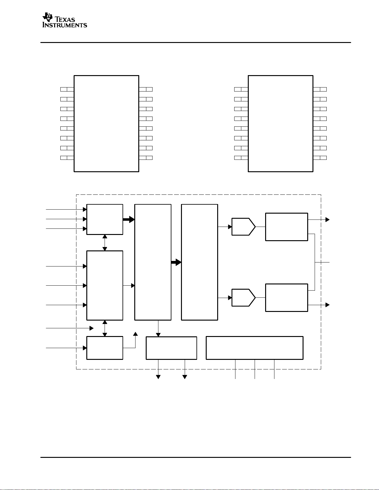
PIN ASSIGNMENTS
PCM1753
PCM1754
PCM1755
SLES092A – OCTOBER 2003 – REVISED AUGUST 2004
PCM1753/PCM1755
(TOP VIEW)
BCK
DATA
LRCK
DGND
NC
V
CC
V
OUT
V
OUT
1
2
3
4
5
6
L
R
7
8
16
15
14
13
12
11
10
9
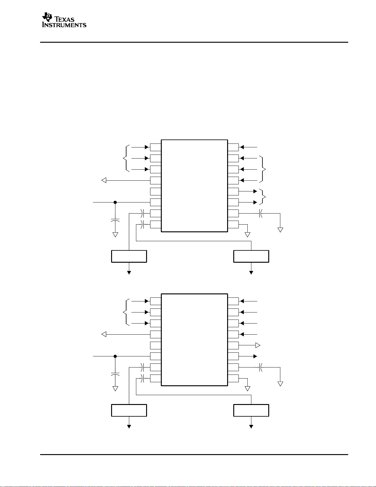
FUNCTIONAL BLOCK DIAGRAM
BCK
LRCK
DATA
Audio
Serial
Port
SCK
ML
MC
MD
ZEROL/NA
ZEROR/ZEROA
V
COM
AGND
BCK
DATA
LRCK
DGND
NC
V
CC
V
OUT
V
OUT
PCM1754
(TOP VIEW)
1
2
3
4
5
6
L
R
DAC
7
8
Output Amp
and
Low-Pass Filter
16
15
14
13
12
11
10
SCK
FMT
MUTE
DEMP
TEST
ZEROA
V
COM
9
AGND
V
OUT
L
(FMT) ML
(MUTE) MC
(DEMP) MD
(TEST)
SCK
†
Open-Drain Output for the PCM1755
( ): PCM1754
Serial
Control
Port
System
Clock
Manager
Oversampling
Digital
Function
Control
System Clock
4y/8y
Filter
and
Zero Detect
†
ZEROL/NA
Enhanced
Multilevel
Delta-Sigma
Modulator
†
(ZEROA)
ZEROR/ZEROA
DAC
Power Supply
CC
DGND
V
Output Amp
and
Low-Pass Filter
AGND
V
V
COM
OUT
R
5
Page 6
PCM1753
PCM1754
PCM1755
SLES092A – OCTOBER 2003 – REVISED AUGUST 2004
www.ti.com
Terminal Functions
TERMINAL
NAME NO.
I/O DESCRIPTION
PCM1753/PCM1755
AGND 9 – Analog ground
BCK 1 I Audio data bit clock input
DATA 2 I Audio data digital input
DGND 4 – Digital ground
LRCK 3 I L-channel and R-channel audio data latch enable input
MC 14 I Mode control clock input
MD 13 I Mode control data input
ML 15 I Mode control latch input
(1)
(1)
(1)
NC 5 –
SCK 16 I System clock input
V
CC
V
COM
V
L 7 O Analog output for L-channel
OUT
V
R 8 O Analog output for R-channel
OUT
6 – Analog power supply, 5 V
10 – Common voltage decoupling
ZEROR/ZEROA 11 O Zero flag output for R-channel/Zero flag output for L-/R-channels
ZEROL/NA 12 O Zero flag output for L-channel/Not assigned
(2)
PCM1754
AGND 9 – Analog ground
BCK 1 I Audio-data bit-clock input
DATA 2 I Audio-data digital input
DEMP 13 I De-emphasis control
(1)
DGND 4 – Digital ground
FMT 15 I Data format select
(1)
LRCK 3 I L-channel and R-channel audio data latch enable input
MUTE 14 I Analog mixing control
(1)
NC 5 –
SCK 16 I System clock input
TEST 12 I Test pin. Ground or open
V
CC
V
COM
V
L 7 O Analog output for L-channel
OUT
V
R 8 O Analog output for R-channel
OUT
6 – Analog power supply, 5 V
10 – Common voltage decoupling
(1)
ZEROA 11 O Zero flag output for L/R channels
(1)
Schmitt-trigger input with internal pulldown.
(2)
Open-drain output (PCM1755).
(2)
6
Page 7

www.ti.com
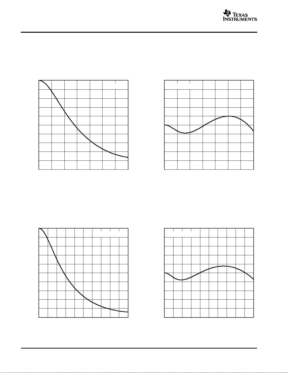
TYPICAL PERFORMANCE CURVES
DIGITAL FILTER (DE-EMPHASIS OFF)
PCM1753
PCM1754
PCM1755
SLES092A – OCTOBER 2003 – REVISED AUGUST 2004
AMPLITUDE
vs
FREQUENCY
0
−20
−40
−60
−80
Amplitude – dB
−100
−120
−140
01234
Frequency [× fS]
Figure 1. Frequency Response, Sharp Rolloff
AMPLITUDE
vs
FREQUENCY
0.05
0.04
0.03
0.02
0.01
0.00
−0.01
Amplitude – dB
−0.02
−0.03
−0.04
−0.05
0.0 0.1 0.2 0.3 0.4 0.5
Frequency [× fS]
Figure 2. Pass-Band Ripple, Sharp Rolloff
AMPLITUDE
vs
FREQUENCY
0
−20
−40
−60
−80
Amplitude – dB
−100
−120
−140
01234
Frequency [× fS]
Figure 3. Frequency Response, Slow Rolloff
AMPLITUDE
vs
FREQUENCY
5
4
3
2
1
0
−1
Amplitude – dB
−2
−3
−4
−5
0.0 0.1 0.2 0.3 0.4 0.5
Frequency [× fS]
Figure 4. Transition Characteristics,
Slow Rolloff
All specifications at TA = 25_C, VCC = 5 V , fS = 44.1 kHz, system clock = 384 fS, and 24-bit data, unless otherwise noted
7
Page 8
PCM1753
PCM1754
PCM1755
SLES092A – OCTOBER 2003 – REVISED AUGUST 2004
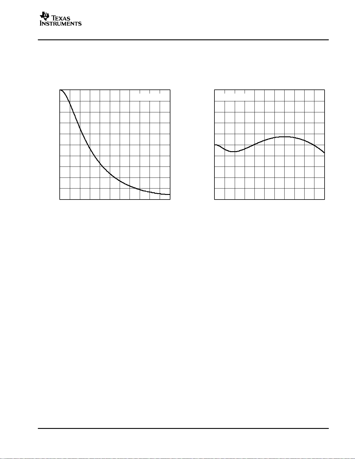
DE-EMPHASIS CURVES
www.ti.com
DE-EMPHASIS LEVEL
vs
FREQUENCY
0
−1
−2
−3
−4
−5
−6
−7
De-emphasis Level – dB
−8
−9
−10
02468101214
f – Frequency – kHz
fS = 32 kHz
Figure 5
DE-EMPHASIS ERROR
vs
FREQUENCY
0.5
fS = 32 kHz
0.4
0.3
0.2
0.1
0.0
−0.1
−0.2
De-emphasis Error – dB
−0.3
−0.4
−0.5
0 2 4 6 8 10 12 14
f – Frequency – kHz
Figure 6
DE-EMPHASIS LEVEL
vs
FREQUENCY
0
−1
−2
−3
−4
−5
−6
−7
De-emphasis Level – dB
−8
−9
−10
02468101214161820
f – Frequency – kHz
fS = 44.1 kHz
0.5
fS = 44.1 kHz
0.4
0.3
0.2
0.1
0.0
−0.1
−0.2
De-emphasis Error – dB
−0.3
−0.4
−0.5
0 2 4 6 8 101214161820
Figure 7
All specifications at TA = 25_C, VCC = 5 V , fS = 44.1 kHz, system clock = 384 fS, and 24-bit data, unless otherwise noted
DE-EMPHASIS ERROR
vs
FREQUENCY
f – Frequency – kHz
Figure 8
8
Page 9
www.ti.com
DE-EMPHASIS CURVES (CONTINUED)
PCM1753
PCM1754
PCM1755
SLES092A – OCTOBER 2003 – REVISED AUGUST 2004
DE-EMPHASIS LEVEL
vs
FREQUENCY
0
−1
−2
−3
−4
−5
−6
−7
De-emphasis Level – dB
−8
−9
−10
0 2 4 6 8 10121416182022
f – Frequency – kHz
fS = 48 kHz
0.5
fS = 48 kHz
0.4
0.3
0.2
0.1
0.0
−0.1
−0.2
De-emphasis Error – dB
−0.3
−0.4
−0.5
0 2 4 6 8 10121416182022
Figure 9
All specifications at TA = 25_C, VCC = 5 V , fS = 44.1 kHz, system clock = 384 fS, and 24-bit data, unless otherwise noted
DE-EMPHASIS ERROR
vs
FREQUENCY
f – Frequency – kHz
Figure 10
9
Page 10
PCM1753
PCM1754
PCM1755
SLES092A – OCTOBER 2003 – REVISED AUGUST 2004
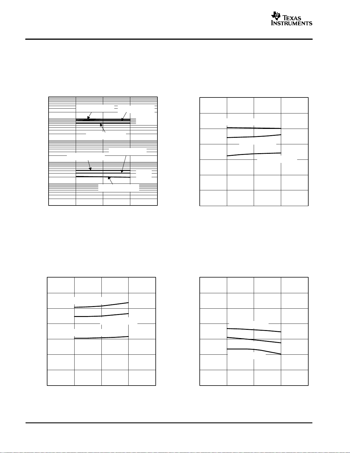
ANALOG DYNAMIC PERFORMANCE (SUPPLY VOLTAGE CHARACTERISTICS)
www.ti.com
TOTAL HARMONIC DISTORTION + NOISE
vs
SUPPLY VOLTAGE
10
192 kHz, 128 f
1
44.1 kHz, 384 f
0.1
192 kHz, 128 f
0.01
0.001
THD+N – Total Harmonic Distortion + Noise – %
0.0001
4.0 4.5 5.0 5.5 6.0
VCC – Supply Voltage – V
S
96 kHz, 384 f
S
96 kHz, 384 f
S
44.1 kHz, 384 f
Figure 11
S
S
–60 dB
S
0 dB
DYNAMIC RANGE
vs
SUPPLY VOLTAGE
110
108
44.1 kHz, 384 f
106
104
102
Dynamic Range – dB
100
98
96
4.0 4.5 5.0 5.5 6.0
VCC – Supply Voltage – V
S
96 kHz, 384 f
192 kHz, 128 f
S
Figure 12
S
SIGNAL-to-NOISE RATIO
vs
SUPPLY VOLTAGE
110
108
44.1 kHz, 384 f
106
104
192 kHz, 128 f
102
100
SNR – Signal-to-Noise Ratio – dB
98
96
4.0 4.5 5.0 5.5 6.0
VCC – Supply Voltage – V
S
96 kHz, 384 f
S
S
110
108
106
104
102
100
Channel Separation – dB
98
96
4.0 4.5 5.0 5.5 6.0
Figure 13
All specifications at TA = 25_C, VCC = 5 V , fS = 44.1 kHz, system clock = 384 fS, and 24-bit data, unless otherwise noted
CHANNEL SEPARATION
vs
SUPPLY VOLTAGE
44.1 kHz, 384 f
96 kHz, 384 f
192 kHz, 128 f
VCC – Supply Voltage – V
Figure 14
S
S
S
10
Page 11

www.ti.com
SLES092A – OCTOBER 2003 – REVISED AUGUST 2004
ANALOG DYNAMIC PERFORMANCE (TEMPERATURE CHARACTERISTICS)
PCM1753
PCM1754
PCM1755
TOTAL HARMONIC DISTORTION + NOISE
vs
FREE-AIR TEMPERATURE
10
192 kHz, 128 f
1
0.1
192 kHz, 128 f
0.01
0.001
THD+N – Total Harmonic Distortion + Noise – %
0.0001
−50 −25 0 25 50 75 100
S
96 kHz, 384 f
44.1 kHz, 384 f
S
96 kHz, 384 f
44.1 kHz, 384 f
TA – Free-Air Temperature – °C
S
S
Figure 15
DYNAMIC RANGE
vs
FREE-AIR TEMPERATURE
110
S
–60 dB
S
0 dB
108
44.1 kHz, 384 f
106
104
102
Dynamic Range – dB
100
98
96
−50 −25 0 25 50 75 100
96 kHz, 384 f
TA – Free-Air Temperature – °C
S
S
192 kHz, 128 f
S
Figure 16
SIGNAL-to-NOISE RATIO
vs
FREE-AIR TEMPERATURE
110
108
44.1 kHz, 384 f
106
104
102
100
SNR – Signal-to-Noise Ratio – dB
98
96
−50 −25 0 25 50 75 100
TA – Free-Air Temperature – °C
S
96 kHz, 384 f
192 kHz, 128 f
S
S
110
108
106
104
102
100
Channel Separation – dB
98
96
−50 −25 0 25 50 75 100
Figure 17
All specifications at TA = 25_C, VCC = 5 V , fS = 44.1 kHz, system clock = 384 fS, and 24-bit data, unless otherwise noted
–25°C to 85°C for the PCM1753/55, –40°C to 85°C for the PCM1754
.
CHANNEL SEPARATION
vs
FREE-AIR TEMPERATURE
96 kHz, 384 f
S
TA – Free-Air Temperature – °C
44.1 kHz, 384 f
Figure 18
192 kHz, 128 f
S
S
11
Page 12

PCM1753
PCM1754
PCM1755
SLES092A – OCTOBER 2003 – REVISED AUGUST 2004
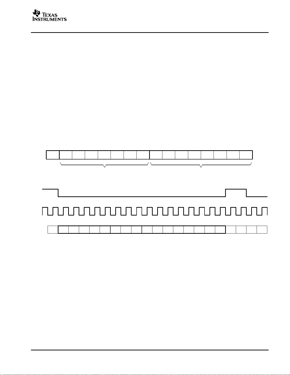
SYSTEM CLOCK AND RESET FUNCTIONS
System Clock Input
The PCM1753/54/55 requires a system clock for operating the digital interpolation filters and multilevel
delta-sigma modulators. The system clock is applied at the SCK input (pin 16). Table 1 shows examples of
system clock frequencies for common audio sampling rates.
Figure 19 shows the timing requirements for the system clock input. For optimal performance, it is important
to use a clock source with low phase-jitter and noise. TI’s PLL170x family of multiclock generators is an excellent
choice for providing the PCM1753/54/55 system clock.
Table 1. System Clock Rates for Common Audio Sampling Frequencies
www.ti.com
SAMPLING FREQUENCY SYSTEM CLOCK FREQUENCY (f
128 f
S
8 kHz 1.0240 1.5360 2.0480 3.0720 4.0960 6.1440 9.2160
16 kHz 2.0480 3.0720 4.0960 6.1440 8.1920 12.2880 18.4320
32 kHz 4.0960 6.1440 8.1920 12.2880 16.3840 24.5760 36.8640
44.1 kHz 5.6448 8.4672 11.2896 16.9344 22.5792 33.8688 (1)
48 kHz 6.1440 9.2160 12.2880 18.4320 24.5760 36.8640 (1)
88.2 kHz 11.2896 16.9344 22.5792 33.8688 45.1584 (1) (1)
96 kHz 12.2880 18.4320 24.5760 36.8640 49.1520 (1) (1)
192 kHz 24.5760 36.8640 49.1520 (1) (1) (1) (1)
(1)
This system clock rate is not supported for the given sampling frequency.
H
System Clock (SCK)
L
PARAMETERS SYMBOL MIN TYP MAX UNITS
System clock pulse duration, high t
System clock pulse duration, low t
System clock pulse cycle time t
(1)
1/128 fS, 1/256 fS, 1/384 fS, 1/512 fS, 1/768 fS, or 1/1152 f
192 f
t
(SCKL)
256 f
S
t
S
S
(SCKH)
384 f
S
Figure 19. System Clock Input Timing
SCLK
512 f
t
(SCY)
(SCKH)
(SCKL)
(SCY)
) (MHz)
S
768 f
S
2.0 V
0.8 V
7 ns
7 ns
(1)
1152 f
S
ns
12
Page 13

www.ti.com
SLES092A – OCTOBER 2003 – REVISED AUGUST 2004
Power-On Reset Functions
The PCM1753/54/55 includes a power-on reset function. Figure 20 shows the operation of this function. With
the system clock active and V
> 3 V (typical, 2.2 V to 3.7 V), the power-on reset function is enabled. The
CC
initialization sequence requires 1024 system clocks from the time VCC > 3 V (typical, 2.2 V to 3.7 V). After the
initialization period, the PCM1753/55 is set to its reset default state, as described in the Mode Control Registers
section of this data sheet.
During the reset period (1024 system clocks), the analog output is forced to the bipolar zero level, or VCC/2.
After the reset period, an internal register is initialized in the next 1/fS period and if SCK, BCK, and LRCK are
provided continuously, the PCM1753/54/55 provides proper analog output with unit group delay against the
input data.
V
CC
3.7 V (Max)
3.0 V (Typ)
2.2 V (Min)
Reset Reset Removal
Internal Reset
PCM1753
PCM1754
PCM1755
System Clock
Don’t Care
1024 System Clocks
Figure 20. Power-On Reset Timing
13
Page 14

PCM1753
PCM1754
PCM1755
SLES092A – OCTOBER 2003 – REVISED AUGUST 2004
AUDIO SERIAL INTERFACE
The audio serial interface for the PCM1753/54/55 consists of a 3-wire synchronous serial port. It includes LRCK
(pin 3), BCK (pin 1), and DATA (pin 2). BCK is the serial audio bit clock, and it is used to clock the serial data
present on DATA into the serial shift register of the audio interface. Serial data is clocked into the
PCM1753/54/55 on the rising edge of BCK. LRCK is the serial audio left/right word clock. It is used to latch serial
data into the internal registers of the serial audio interface.
Both LRCK and BCK should be synchronous to the system clock. Ideally, it is recommended that LRCK and
BCK be derived from the system clock input, SCK. LRCK is operated at the sampling frequency, fS. BCK can
be operated at 32, 48, or 64 times the sampling frequency for standard and left-justified formats. BCK can be
operated at 48 or 64 times the sampling frequency for the I2S format.
Internal operation of the PCM1753/54/55 is synchronized with LRCK. Accordingly, internal operation is held
when the sampling rate clock of LRCK is changed or when SCK and/or BCK is interrupted for a 3-bit clock cycle
or longer. If SCK, BCK, and LRCK are provided continuously after this held condition, the internal operation is
re-synchronized automatically in a period of less than 3/fS. External resetting is not required.
Audio Data Formats and Timing
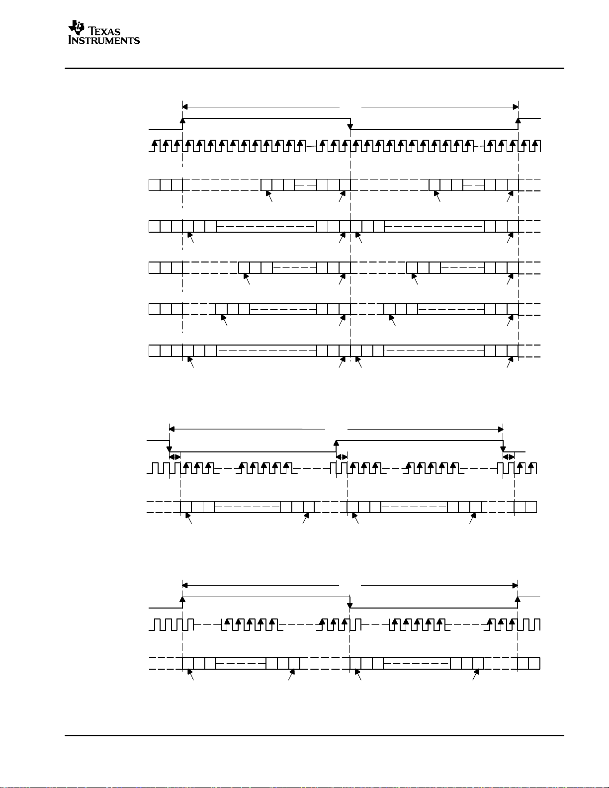
The PCM1753/55 supports industry-standard audio data formats, including standard, I2S, and left-justified. The
PCM1754 supports I2S and 16-bit-word right-justified. The data formats are shown in Figure 22. Data formats
are selected using the format bits, FMT[2:0], located in control register 20 of the PCM1753/55, and are selected
using the FMT pin on the PCM1754. The default data format is 24-bit left-justified. All formats require binary
2s-complement, MSB-first audio data. Figure 21 shows a detailed timing diagram for the serial audio interface.
www.ti.com
LRCK
t
(BCH)
BCK
t
DATA
t
(DS)
PARAMETERS SYMBOL MIN MAX UNITS
BCK pulse cycle time t
BCK high-level time t
BCK low-level time t
BCK rising edge to LRCK edge t
LRCK falling edge to BCK rising edge t
DATA setup time t
DATA hold time t
(1)
fS is the sampling frequency (e.g., 44.1 kHZ, 48 kHz, 96 kHz, etc.).
(BCY)
t
(BCL)
t
(BL)
t
(DH)
Figure 21. Audio Interface Timing
(BCY)
(BCH)
(BCL)
(BL)
(LB)
(DS)
(DH)
t
(LB)
1/(32 fS), 1/(48 fS),
1/(64 fS)
1.4 V
1.4 V
1.4 V
(1)
35 ns
35 ns
10 ns
10 ns
10 ns
10 ns
14
Page 15
www.ti.com
(1) Standard Data Format; L-Channel = HIGH, R-Channel = LOW
LRCK
BCK
(= 32 fS, 48 fS, or 64 fS)
16-Bit Right-Justified, BCK = 48 fS or 64 f
DATA 14 15 16 123 14 15 16
S
L-Channel R-Channel
PCM1753
PCM1754
PCM1755
SLES092A – OCTOBER 2003 – REVISED AUGUST 2004
1/f
S
123 14 15 16
MSB LSB
16-Bit Right-Justified, BCK = 32 f
14 15 16 123 14 15 16
DATA
18-Bit Right-Justified, BCK = 48 fS or 64 f
16 17 18
DATA
20-Bit Right-Justified, BCK = 48 fS or 64 f
18 19 20 123 18 19 20
DATA
24-Bit Right-Justified, BCK = 48 fS or 64 f
DATA
22 23 24 123
S
MSB LSB
S
123 16 17 18
MSB LSB
S
MSB LSB
S
MSB LSB
(2) I2S Data Format; L-Channel = LOW, R-Channel = HIGH
L-Channel R-ChannelLRCK
BCK
(= 48 fS or 64 fS)
22 23 24
1/f
S
MSB LSB
123 14 15 16
MSB LSB
123 16 17 18
MSB LSB
123 18 19 20
MSB LSB
123 22 23 24
MSB LSB
DATA
123 12
MSB
N–2NN–1
LSB
(3) Left-Justified Data Format; L-Channel = HIGH, R-Channel = LOW
LRCK
BCK
(= 32 fS, 48 fS, or 64 fS)
DATA 123
MSB LSB LSBMSB
L-Channel R-Channel
N–2NN–1
Figure 22. Audio Data Input Formats
123
MSB
1/f
S
123
N–2NN–1
LSB
N–2NN–1
12
15
Page 16
PCM1753
PCM1754
PCM1755
SLES092A – OCTOBER 2003 – REVISED AUGUST 2004
ZERO FLAGS (PCM1753/55)
Zero-Detect Condition
Zero detection for either output channel is independent from the other channel. If the data for a given channel
remains at a 0 level for 1024 sample periods (or LRCK clock periods), a zero-detect condition exists for that
channel.
Zero Flag Outputs
If a zero-detect condition exists for one or more channels, the zero flag pins for those channels are set to a logic
1 state. There are zero flag pins for each channel, ZEROL (pin 12) and ZEROR (pin 11). These pins can be
used to operate external mute circuits, or used as status indicators for a microcontroller, audio signal processor,
or other digitally controlled function.
The active polarity of zero flag outputs can be inverted by setting the ZREV bit of control register 22 to 1. The
reset default is active-high output, or ZREV = 0.
The L-channel and R-channel common zero flag can be selected by setting the AZRO bit of control register
22 to 1. The reset default is independent zero flags for L-channel and R-channel, or AZRO = 0.
In the case of the PCM1755, ZEROL and ZEROR are open-drain outputs.
www.ti.com
ZERO FLAG (PCM1754)
The PCM1754 has a ZERO flag pin, ZEROA (pin 1 1). ZEROA is the L-channel and R-channel common zero
flag pin. If the data for L-channel and R-channel remains at a 0 level for 1024 sampling periods (or LRCK clock
periods), ZEROA is set to a logic 1 state.
HARDWARE CONTROL (PCM1754)
The digital functions of the PCM1754 are capable of hardware control. Table 2 shows selectable formats,
Table 3 shows de-emphasis control, and Table 4 shows mute control.
Table 2. Data Format Select
FMT (PIN 15) DATA FORMAT
LOW 16- to 24-bit, I2S format
HIGH 16-bit right-justified
Table 3. De-Emphasis Control
DEMP (PIN 13) DE-EMPHASIS FUNCTION
LOW 44.1 kHz de-emphasis OFF
HIGH 44.1 kHz de-emphasis ON
Table 4. Mute Control
MUTE (PIN 14) MUTE
LOW Mute OFF
HIGH Mute ON
OVERSAMPLING RATE CONTROL (PCM1754)
The PCM1754 automatically controls the oversampling rate of the delta-sigma D/A converters with the system
clock rate. The oversampling rate is set to 64× oversampling with every system clock and sampling frequency .
16
Page 17
www.ti.com
SLES092A – OCTOBER 2003 – REVISED AUGUST 2004
SOFTWARE CONTROL (PCM1753/55)
The PCM1753/55 has many programmable functions which can be controlled in the software control mode. The
functions are controlled by programming the internal registers using ML, MC, and MD.
The serial control interface is a 3-wire serial port, which operates asynchronously to the audio serial interface.
The serial control interface is used to program the on-chip mode registers. The control interface includes MD
(pin 13), MC (pin 14), and ML (pin 15). MD is the serial data input, used to program the mode registers. MC
is the serial bit clock, used to shift data into the control port. ML is the control port latch clock.
Register Write Operation
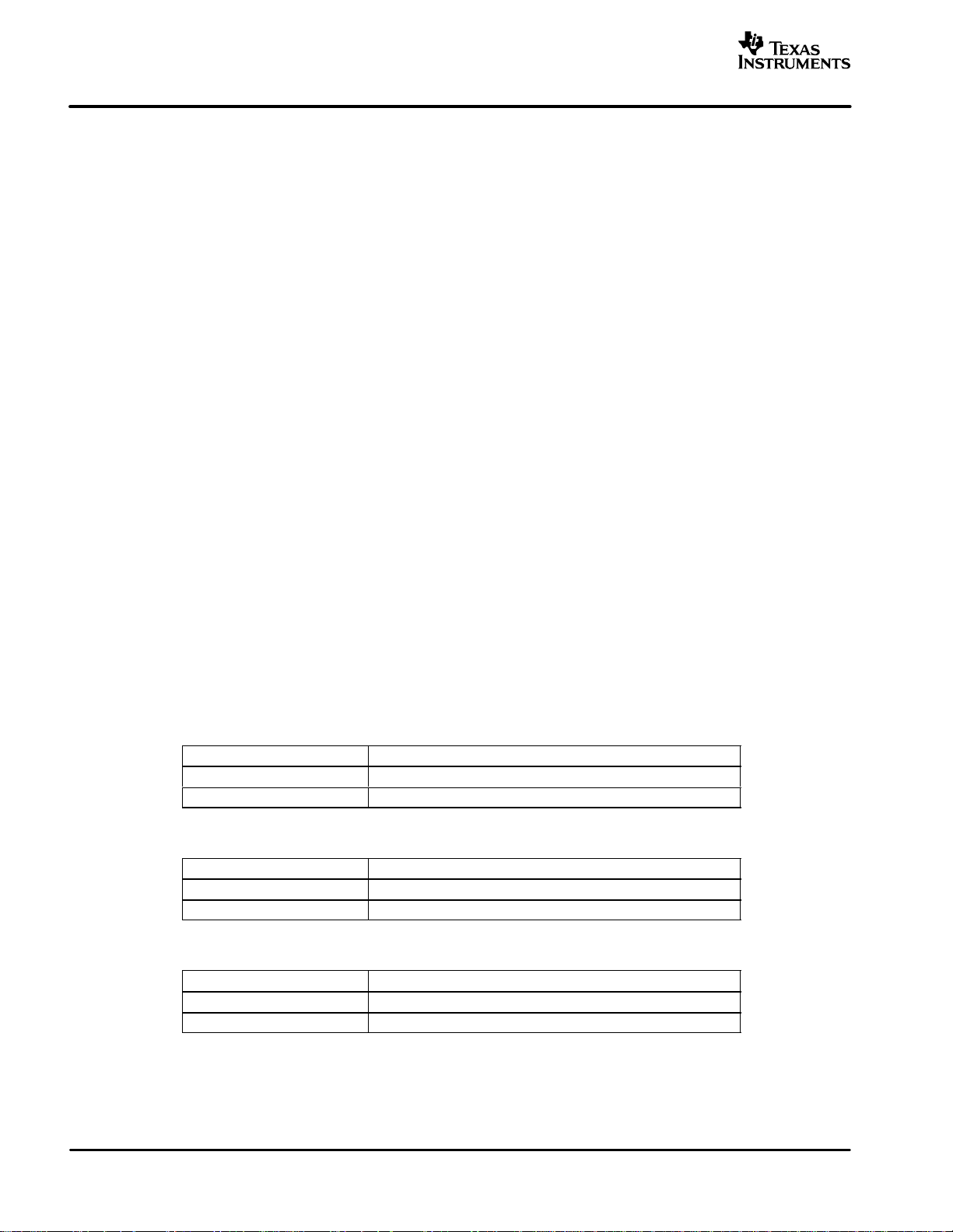
All write operations for the serial control port use 16-bit data words. Figure 23 shows the control data word
format. The most significant bit must be a 0. There are seven bits, labeled IDX[6:0], that set the register index
(or address) for the write operation. The least significant eight bits, D[7:0], contain the data to be written to the
register specified by IDX[6:0].
Figure 24 shows the functional timing diagram for writing to the serial control port. ML is held at a logic 1 state
until a register needs to be written. To start the register write cycle, ML is set to logic 0. Sixteen clocks are then
provided on MC, corresponding to the 16 bits of the control data word on MD. After the sixteenth clock cycle
has completed, ML is set to logic 1 to latch the data into the indexed mode control register.
MSB
0 IDX6 IDX5 IDX4 IDX3 IDX2 IDX1 IDX0 D7 D6 D4D5 D3 D2 D1 D0
PCM1753
PCM1754
PCM1755
LSB
Register Index (or Address) Register Data
Figure 23. Control Data Word Format for MD
ML
MC
IDX0
MD X 0
X
IDX1IDX2IDX3IDX4IDX5IDX6
D7 D6 D4D5 D3 D2 D1 D00
X
Figure 24. Register Write Operation
IDX6
17
Page 18
PCM1753
PCM1754
PCM1755
SLES092A – OCTOBER 2003 – REVISED AUGUST 2004
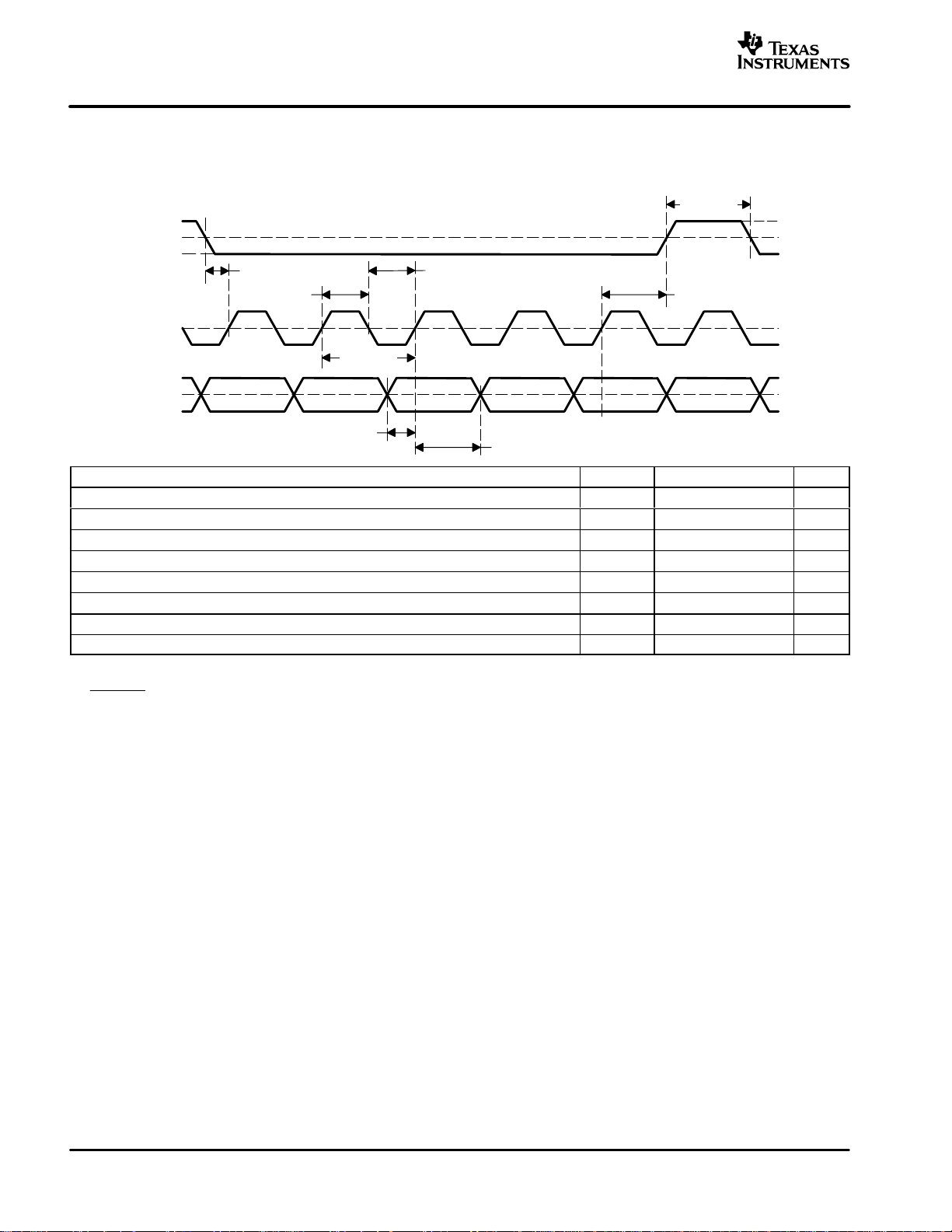
Control Interface Timing Requirements
Figure 25 shows a detailed timing diagram for the serial control interface. These timing parameters are critical
for proper control port operation.
t
(MHH)
ML
www.ti.com
t
(MLS)
t
(MCH)
t
(MCL)
MC
t
(MCY)
MD
t
(MDS)
t
(MDH)
PARAMETERS SYMBOL MIN TYP MAX UNITS
MC pulse cycle time t
MC low-level time t
MC high-level time t
ML high-level time t
ML falling edge to MC rising edge t
ML hold time
(1)
MD hold time t
MD setup time t
(1)
MC rising edge for LSB to ML rising edge.
3
(2)
256 f
sec (min); fS: sampling rate
S
LSB
(MCY)
(MCL)
(MCH)
(MHH)
(MLS)
t
(MLH)
(MDH)
(MDS)
t
(MLH)
100 ns
50 ns
50 ns
(2)
ns
20 ns
20 ns
15 ns
20 ns
18
Figure 25. Control Interface Timing
Page 19

PCM1753
PCM1754
www.ti.com
SLES092A – OCTOBER 2003 – REVISED AUGUST 2004
MODE CONTROL REGISTERS (PCM1753/55)
User-Programmable Mode Controls
The PCM1753/55 includes a number of user programmable functions, which are accessed via control registers.
The registers are programmed using the serial control interface, which was previously discussed in this data
sheet. T able 5 lists the available mode control functions, along with their reset default conditions and associated
register index.
Register Map
The mode control register map is shown in Table 6. Each register includes an index (or address) indicated by
the IDX[6:0] bits.
Table 5. User-Programmable Mode Controls
FUNCTION RESET DEFAULT REGISTER BIT(s)
Digital attenuation control, 0 dB to –63 dB in 0.5-dB steps 0 dB, no attenuation 16 and 17 AT1[7:0], AT2[7:0]
Soft mute control Mute disabled 18 MUT[2:0]
Oversampling rate control (64 fS or 128 fS) 64 fS oversampling 18 OVER
Soft reset control Reset disabled 18 SRST
DAC operation control DAC1 and DAC2 enabled 19 DAC[2:1]
De-emphasis function control De-emphasis disabled 19 DM12
De-emphasis sample rate selection 44.1 kHz 19 DMF[1:0]
Audio data format control 24-bit left-justified 20 FMT[2:0]
Digital filter rolloff control Sharp rolloff 20 FLT
Zero flag function select L-, R-channel independent 22 AZRO
Output phase select Normal phase 22 DREV
Zero flag polarity select High 22 ZREV
PCM1755
Table 6. Mode Control Register Map
IDX
(B8–B14)
10h Register 16 0 IDX6 IDX5 IDX4 IDX3 IDX2 IDX1 IDX0 AT17 AT16 AT15 AT14 AT13 AT12 AT11 AT10
12h Register 18 0 IDX6 IDX5 IDX4 IDX3 IDX2 IDX1 IDX0 SRST OVER RSV RSV RSV RSV MUT2 MUT1
13h Register 19 0 IDX6 IDX5 IDX4 IDX3 IDX2 IDX1 IDX0 RSV DMF1 DMF0 DM12 RSV RSV DAC2 DAC1
14h Register 20 0 IDX6 IDX5 IDX4 IDX3 IDX2 IDX1 IDX0 RSV RSV FLT RSV RSV FMT2 FMT1 FMT0
16h Register 22 0 IDX6 IDX5 IDX4 IDX3 IDX2 IDX1 IDX0 RSV RSV RSV RSV RSV AZRO ZREV DREV
NOTE:RSV: Reserved for test operation. It should be set to 0 for regular operation.
REGISTER B15 B14 B13 B12 B11 B10 B9 B8 B7 B6 B5 B4 B3 B2 B1 B0
11h Register 17 0 IDX6 IDX5 IDX4 IDX3 IDX2 IDX1 IDX0 AT27 AT26 AT25 AT24 AT23 AT22 AT21 AT20
19
Page 20
PCM1753
PCM1754
PCM1755
SLES092A – OCTOBER 2003 – REVISED AUGUST 2004
Register Definitions
B15 B14 B13 B12 B11 B10 B9 B8 B7 B6 B5 B4 B3 B2 B1 B0
Register 16 0 IDX6 IDX5 IDX4 IDX3 IDX2 IDX1 IDX0 AT17 AT16 AT15 AT14 AT13 AT12 AT11 AT10
B15 B14 B13 B12 B11 B10 B9 B8 B7 B6 B5 B4 B3 B2 B1 B0
Register 17
ATx[7:0]: Digital Attenuation Level Setting
0 IDX6 IDX5 IDX4 IDX3 IDX2 IDX1 IDX0 AT27 AT26 AT25 AT24 AT23 AT22 AT21 AT20
www.ti.com
Where x = 1 or 2, corresponding to the DAC output V
L (x = 1) and V
OUT
R (x = 2).
OUT
Default value: 1111 1111b
Each DAC channel (V
OUT
L and V
R) includes a digital attenuation function. The attenuation level can be
OUT
set from 0 dB to –63 dB in 0.5-dB steps. Changes in attenuator levels are made by incrementing or
decrementing one step (0.5 dB) for every 8/fS time internal until the programmed attenuator setting is reached.
Alternatively, the attenuation level can be set to infinite attenuation (or mute).
The attenuation data for each channel can be set individually. The attenuation level is set using the following
formula:
Attenuation level (dB) = 0.5 × (ATx[7:0]
where ATx[7:0]
For ATx[7:0]
= 0 through 255.
DEC
= 0 through 128, attenuation is set to infinite attenuation.
DEC
DEC
– 255)
The following table shows the attenuation levels for various settings:
ATx[7:0] DECIMAL VALUE ATTENUATION LEVEL SETTING
1111 1111b 255 0 dB, No Attenuation. (default)
1111 1110b 254 –0.5 dB
1111 1101b 253 –1.0 dB
L LL
1000 0011b 131 –62.0 dB
1000 0010b 130 –62.5 dB
1000 0001b 129 –63.0 dB
1000 0000b 128 Mute
L LL
0000 0000
B
0 Mute
B15 B14 B13 B12 B11 B10 B9 B8 B7 B6 B5 B4 B3 B2 B1 B0
Register 18
0 IDX6 IDX5 IDX4 IDX3 IDX2 IDX1 IDX0 SRST OVER RSV RSV RSV RSV MUT2 MUT1
MUTx: Soft Mute Control
where x = 1 or 2, corresponding to the DAC outputs V
L (x = 1) and V
OUT
R (x = 2).
OUT
Default value: 0
MUTx = 0
Mute disabled (default)
MUTx = 1 Mute enabled
The mute bits, MUT1 and MUT2, are used to enable or disable the soft mute function for the corresponding
DAC outputs, V
OUT
L and V
R. The soft mute function is incorporated into the digital attenuators. When mute
OUT
is disabled (MUTx = 0), the attenuator and DAC operate normally. When mute is enabled by setting MUTx = 1,
the digital attenuator for the corresponding output is decreased from the current setting to infinite attenuation,
one attenuator step (0.5 dB) for every 8/fS seconds. This provides pop-free muting of the DAC output.
20
Page 21
PCM1753
PCM1754
www.ti.com
SLES092A – OCTOBER 2003 – REVISED AUGUST 2004
By setting MUTx = 0, the attenuator is increased one step for every 8/fS seconds to the previously programmed
attenuation level.
OVER: Oversampling Rate Control
Default value: 0
PCM1755
System clock rate = 256 f
OVER = 0
64× oversampling (default)
, 384 fS, 512 fS, 768 fS, or 1152 fS:
S
OVER = 1 128× oversampling
System clock rate = 128 fS or 192 fS:
OVER = 0
32× oversampling (default)
OVER = 1 64× oversampling
The OVER bit is used to control the oversampling rate of the delta-sigma D/A converters. The OVER = 1 setting
is recommended when the sampling rate is 192 kHz (system clock rate is 128 fS or 192 fS).
SRST: Reset
Default value: 0
SRST = 0
Reset disabled (default)
SRST = 1 Reset enabled
The SRST bit is used to enable or disable the soft reset function. The operation is the same as power-on reset.
All registers are initialized.
B15 B14 B13 B12 B11 B10 B9 B8 B7 B6 B5 B4 B3 B2 B1 B0
Register 19
0 IDX6 IDX5 IDX4 IDX3 IDX2 IDX1 IDX0 RSV DMF1 DMF0 DM12 RSV RSV DAC2 DAC1
DACx: DAC Operation Control
Where x = 1 or 2, corresponding to the DAC output V
L (x = 1) or V
OUT
R (x = 2).
OUT
Default value: 0
DACx = 0
DAC operation enabled (default)
DACx = 1 DAC operation disabled
The DAC operation controls are used to enable and disable the DAC outputs, V
OUT
L and V
OUT
R. When
DACx = 0, the corresponding output generates the audio waveform dictated by the data present on the DATA
pin. When DACx = 1, the corresponding output is set to the bipolar zero level, or 0.5 VCC.
DM12: Digital De-Emphasis Function Control
Default value: 0
DM12 = 0
De-emphasis disabled (default)
DM12 = 1 De-emphasis enabled
The DM12 bit is used to enable or disable the digital de-emphasis function. See the plots shown in the Typical
Performance Curves section of this data sheet.
21
Page 22
PCM1753
PCM1754
PCM1755
SLES092A – OCTOBER 2003 – REVISED AUGUST 2004
DMF[1:0]: Sampling Frequency Selection for the De-Emphasis Function
Default value: 00
The DMF[1:0] bits are used to select the sampling frequency used for the digital de-emphasis function when
it is enabled.
www.ti.com
DMF[1:0]
De-Emphasis Sample Rate Selection
00 44.1 kHz (default)
01 48 kHz
10 32 kHz
11 Reserved
B15 B14 B13 B12 B11 B10 B9 B8 B7 B6 B5 B4 B3 B2 B1 B0
Register 20
0 IDX6 IDX5 IDX4 IDX3 IDX2 IDX1 IDX0 RSV RSV FLT RSV RSV FMT2 FMT1 FMT0
FMT[2:0]: Audio Interface Data Format
Default value: 101
The FMT[2:0] bits are used to select the data format for the serial audio interface. The following table shows
the available format options.
FMT[2:0]
Audio Data Format Selection
000 24-bit standard format, right-justified data
001 20-bit standard format, right-justified data
010 18-bit standard format, right-justified data
011 16-bit standard format, right-justified data
100 16- to 24-bit I2S format
101 16- to 24-bit left-justified format (default)
110 Reserved
111 Reserved
FLT: Digital Filter Rolloff Control
Default value: 0
FLT = 0
Sharp rolloff (default)
FLT = 1 Slow rolloff
The FLT bit allows the user to select the digital filter rollof f that is best suited to the application. Two filter rolloff
selections are available, sharp and slow. The filter responses for these selections are shown in the Typical
Performance Curves section of this data sheet.
B15 B14 B13 B12 B11 B10 B9 B8 B7 B6 B5 B4 B3 B2 B1 B0
Register 22
0 IDX6 IDX5 IDX4 IDX3 IDX2 IDX1 IDX0 RSV RSV RSV RSV RSV AZRO ZREV DREV
DREV: Output Phase Select
Default value: 0
DREV = 0
Normal output (default)
DREV = 1 Inverted output
The DREV bit is the output analog signal phase control.
22
Page 23

www.ti.com
ZREV: Zero Flag Polarity Select
Default value: 01h
PCM1753
PCM1754
PCM1755
SLES092A – OCTOBER 2003 – REVISED AUGUST 2004
ZREV = 0
High on zero flag pins indicates a zero detect (default)
ZREV = 1 Low on zero flag pins indicates a zero detect
The ZREV bit allows the user to select the polarity of zero flag pins.
AZRO: Zero Flag Function Select
Default value: 0
AZRO = 0
L-/R-channel independent zero flags (default)
AZRO = 1 L-/R-channel common zero flag
The AZRO bit allows the user to select the function of zero flag pins.
AZRO = 0:
Pin 11: ZEROR, zero flag output for R-channel
Pin 12: ZEROL, zero flag output for L-channel
AZRO = 1: Pin 11: ZEROA, zero flag output for L-/R-channels
Pin 12: NA, not assigned
ANALOG OUTPUTS
The PCM1753/54/55 includes two independent output channels, V
outputs, each capable of driving 4 V p-p typical into a 5-kΩ ac-coupled load. The internal output amplifiers for
V
OUT
L and V
R are biased to the dc common-mode (or bipolar zero) voltage, equal to 0.5 VCC.
OUT
The output amplifiers include an RC continuous-time filter, which helps to reduce the out-of-band noise energy
present at the DAC outputs due to the noise shaping characteristics of the PCM1753/54/55 delta-sigma D/A
converters. The frequency response of this filter is shown in Figure 26. By itself, this filter is not enough to
attenuate the out-of-band noise to an acceptable level for many applications. An external low-pass filter is
required to provide sufficient out-of-band noise rejection. Further discussion of DAC post-filter circuits is
provided in the Applications Information section of this data sheet.
OUT
L and V
R. These are unbalanced
OUT
LEVEL
vs
FREQUENCY
10
0
−10
−20
−30
Level – dB
−40
−50
−60
0.1 100 1k 10k1 10
f – Frequency – kHz
Figure 26. Output Filter Frequency Response
23
Page 24
PCM1753
PCM1754
PCM1755
SLES092A – OCTOBER 2003 – REVISED AUGUST 2004
V
Output
COM
One unbuffered common-mode voltage output pin, V
pin is nominally biased to a dc voltage level equal to 0.5 VCC. This pin can be used to bias external circuits.
Figure 27 shows an example of using the V
PCM1753/54/55
R
1
C
+
10 µF
V
OUT
V
COM
†
X
pin for external biasing applications.
COM
R
2
R
2
(pin 10) is brought out for decoupling purposes. This
COM
R
10 µF
+
R
2
1
Filtered
Output
AV+*1, where AV+*
V
2
3
–
1/2
OPA2353
+
CC
1
C
1
3
www.ti.com
†
X = L or R
(a) Using V
PCM1753/54/55
V
COM
(b) Using a Voltage Follower to Buffer V
to Bias a Single-Supply Filter Stage
COM
V
CC
–
OPA337
+
+
10 µF
When Biasing Multiple Nodes
COM
Figure 27. Biasing External Circuits Using the V
Buffered V
Pin
COM
COM
24
Page 25
www.ti.com
SLES092A – OCTOBER 2003 – REVISED AUGUST 2004
APPLICATION INFORMATION
CONNECTION DIAGRAMS
A basic connection diagram is shown in Figure 28, with the necessary power supply bypassing and decoupling
components. TI recommends using the component values shown in Figure 28 for all designs.
The use of series resistors (22 Ω to 100 Ω) is recommended for the SCK, LRCK, BCK, and DA TA inputs. The
series resistor combines with the stray PCB and device input capacitance to form a low-pass filter, which
reduces high-frequency noise emissions and helps to dampen glitches and ringing present on clock and data
lines.
PCM1753
PCM1754
PCM1755
PCM Audio Data
+5 V
+
10 µF
PCM Audio Data
10 mF
Post LPF
L-Ch Out
+ +
10 mF
1
2
3
4
5
6
7
8
1
2
3
4
BCK
DATA
LRCK
DGND
NC
V
CC
V
OUT
V
OUT
BCK
DATA
LRCK
DGND
PCM1753
PCM1755
L
R
PCM1754
SCK
ML
MC
MD
ZEROL/NA
ZEROR/ZEROA
V
COM
AGND
SCK
FMT
MUTE
DEMP
16
15
14
13
12
11
10
9
16
15
14
13
System Clock
Register Control
Zero Mute Control
+
10 µF
Post LPF
R-Ch Out
System Clock
Format
MUTE On/Off
DEMP On/Off
+5 V
10 µF
+
10 mF
Post LPF
L-Ch Out
+ +
10 mF
NC
5
V
6
CC
V
V
OUT
OUT
L
R
7
8
TEST
ZEROA
V
COM
AGND
12
11
10
9
Post LPF
R-Ch Out
Figure 28. Basic Connection Diagram
Zero Mute Control
+
10 µF
25
Page 26

PCM1753
PCM1754
PCM1755
SLES092A – OCTOBER 2003 – REVISED AUGUST 2004
POWER SUPPLIES AND GROUNDING
The PCM1753/54/55 requires 5 V for VCC.
Proper power supply bypassing is shown in Figure 28. The 10-µF capacitors should be tantalum or aluminum
electrolytic.
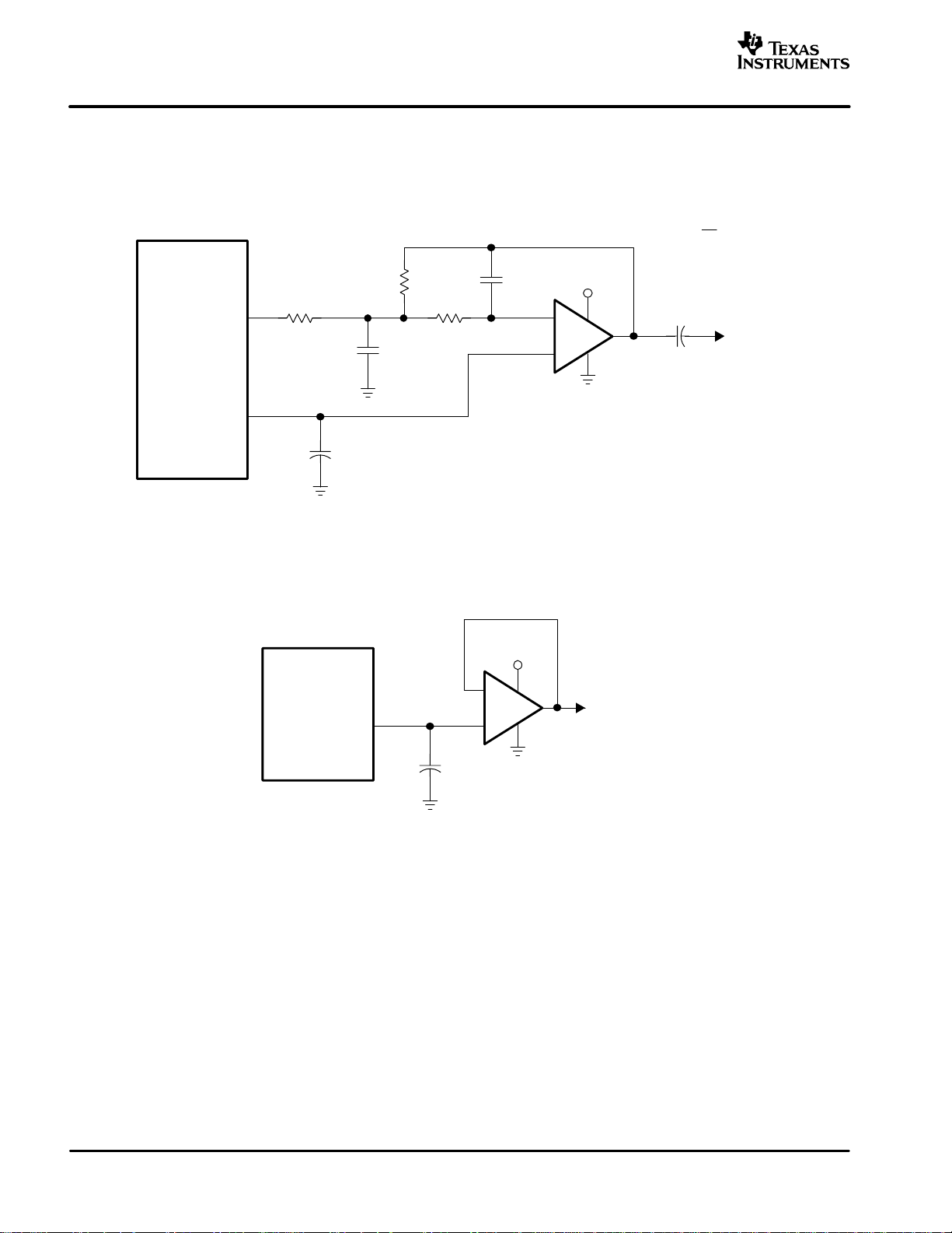
D/A OUTPUT FILTER CIRCUITS
Delta-sigma D/A converters use noise-shaping techniques to improve in-band signal-to-noise ratio (SNR)
performance at the expense of generating increased out-of-band noise above the Nyquist frequency, or fS/2.
The out-of-band noise must be low-pass filtered in order to provide the optimal converter performance. This
is accomplished by a combination of on-chip and external low-pass filtering.
Figure 27(a) and Figure 29 show the recommended external low-pass active filter circuits for single- and
dual-supply applications. These circuits are 2nd-order Butterworth filters using the multiple feedback (MFB)
circuit arrangement, which reduces sensitivity to passive component variations over frequency and
temperature. For more information regarding MFB active filter design, see Burr-Brown applications bulletin
(SBAA055), available from the TI Web site at http://www.ti.com.
Because the overall system performance is defined by the quality of the D/A converters and their associated
analog output circuitry, high-quality audio operational amplifiers are recommended for the active filters. TI’s
OPA2353 and OPA2134 dual operational amplifiers are shown in Figure 27(a) and Figure 29, and are
recommended for use with the PCM1753/54/55.
www.ti.com
V
IN
AV[*
R
2
R
1
R
2
R
1
R
3
C
2
C
1
2
3
–
OPA2134
+
R
1
4
V
OUT
Figure 29. Dual-Supply Filter Circuit
PCB LAYOUT GUIDELINES
A typical PCB floor plan for the PCM1753/54/55 is shown in Figure 30. A ground plane is recommended, with
the analog and digital sections being isolated from one another using a split or cut in the circuit board. The
PCM1753/54/55 should be oriented with the digital I/O pins facing the ground plane split/cut to allow for short,
direct connections to the digital audio interface and control signals originating from the digital section of the
board.
26
Page 27

www.ti.com
PCM1753
PCM1754
PCM1755
SLES092A – OCTOBER 2003 – REVISED AUGUST 2004
Digital Power
+V
Digital Logic
DGND
D
and
Audio
Processor
Digital Section Analog Section
Return Path for Digital Signals
Analog Power
AGND –V
+5VA
V
DGND
PCM1753/54/55
Figure 30. Recommended PCB Layout
CC
AGND
+V
S
S
Output
Circuits
Digital
Ground
Analog
Ground
Separate power supplies are recommended for the digital and analog sections of the board. This prevents the
switching noise present on the digital supply from contaminating the analog power supply and degrading the
dynamic performance of the PCM1753/54/55. In cases where a common 5-V supply must be used for the
analog and digital sections, an inductance (RF choke, ferrite bead) should be placed between the analog and
digital 5-V supply connections to avoid coupling of the digital switching noise into the analog circuitry. Figure 31
shows the recommended approach for single-supply applications.
RF Choke or Ferrite Bead
V
DD
Power Supplies
V
CC
AGND
+V
S
+5V –V
AGND
DGND
PCM1753/54/55
S
Output
Circuits
Digital Section Analog Section
Figure 31. Single-Supply PCB Layout
Common
Ground
27
Page 28

PCM1753
PCM1754
PCM1755
SLES092A – OCTOBER 2003 – REVISED AUGUST 2004
THEORY OF OPERATION
The delta-sigma section of the PCM1753/54/55 is based on an 8-level amplitude quantizer and a 4th-order
noise shaper . This section converts the oversampled input data to 8-level delta-sigma format. A block diagram
of the 8-level delta-sigma modulator is shown in Figure 32. This 8-level delta-sigma modulator has the
advantage of stability and clock jitter sensitivity over the typical one-bit (2-level) delta-sigma modulator.
The combined oversampling rate of the delta-sigma modulator and the interpolation filter is 64 fS.
The theoretical quantization noise performance of the 8-level delta-sigma modulator is shown in Figure 33 and
Figure 34. The enhanced multilevel delta-sigma architecture also has advantages for input clock jitter sensitivity
due to the multilevel quantizer, with the simulated jitter sensitivity shown in Figure 35.
KEY PERFORMANCE PARAMETERS AND MEASUREMENT
This section provides information on how to measure key dynamic performance parameters for the
PCM1753/54/55. In all cases, an Audio Precision System Two Cascade audio measurement system or
equivalent is used to perform the testing.
Total Harmonic Distortion + Noise
Total harmonic distortion + noise (THD+N) is a significant figure of merit for audio D/A converters because it
takes into account both harmonic distortion and all noise sources within a specified measurement bandwidth.
The average value of the distortion and noise is referred to as THD+N.
For the PCM1753/54/55, THD+N is measured with a full-scale, 1-kHz digital sine wave as the test stimulus at
the input of the DAC. The digital generator is set to 24-bit audio word length and a sampling frequency of
44.1 kHz or 96 kHz. The digital generator output is taken from the unbalanced S/PDIF connector of the
measurement system. The S/PDIF data is transmitted via a coaxial cable to the digital audio receiver on the
DEM-DAI1753 demonstration board. The receiver is then configured to output 24-bit data in either I2S or
left-justified data format. The DAC audio interface format is programmed to match the receiver output format.
The analog output is then taken from the DAC post filter and connected to the analog analyzer input of the
measurement system. The analog input is band limited using filters resident in the analyzer. The resulting
THD+N is measured by the analyzer and displayed by the measurement system.
www.ti.com
8 f
OUT
64 f
28
−
+
IN
S
S
+
+
–1
Z
−
+
+
8-Level Quantizer
–1
Z
+
+
+
++
–1
Z
+
+
+
–1
Z
Figure 32. Eight-Level Delta-Sigma Modulator
Page 29

www.ti.com
PCM1753
PCM1754
PCM1755
SLES092A – OCTOBER 2003 – REVISED AUGUST 2004
AMPLITUDE
vs
FREQUENCY
0
−20
−40
−60
−80
−100
Amplitude – dB
−120
−140
−160
−180
012345678
Frequency [ fS]
Figure 33. Quantization Noise Spectrum
( 64 Oversampling)
AMPLITUDE
vs
FREQUENCY
0
−20
−40
−60
−80
−100
Amplitude – dB
−120
−140
−160
−180
012345678
Frequency [ fS]
Figure 34. Quantization Noise Spectrum
( 128 Oversampling)
DYNAMIC RANGE
vs
JITTER
125
120
115
110
105
Dynamic Range – dB
100
95
90
0 100 200 300 400 500 600
Jitter - ps p-p
Figure 35. Jitter Dependence
( 64 Oversampling)
29
Page 30

PCM1753
PCM1754
PCM1755
SLES092A – OCTOBER 2003 – REVISED AUGUST 2004
Dynamic Range
Dynamic range is specified as A-weighted THD+N measured with a –60-dB full-scale, 1-kHz digital sine wave
stimulus at the input of the D/A converter. This measurement is designed to give a good indicator of how the
DAC performs given a low-level input signal.
The measurement setup for the dynamic range measurement is shown in Figure 37, and is similar to the
THD+N test setup discussed previously. The differences include the band limit filter selection, the additional
A-weighting filter, and the –60-dB full-scale input level.
Evaluation Board
DEM-DAI1753
www.ti.com
2nd-Order
Low-Pass
Filter
= 54 kHz or 108 kHz
AES17 Filter
f
= 20.9 kHz
–3 dB
S/PDIF
Output
Audio Precision System Two
Digital
Generator
0 dB FS
(100% Full-Scale),
24-Bit,
1-kHz Sine Wave
S/PDIF
Receiver
Analyzer
and
Display
Averaging
Mode
PCM1753/54/55
Band Limit
HPF = 400 Hz
LPF = 30 kHz
f
–3 dB
Figure 36. Test Setup for THD+N Measurement
Idle Channel Signal-to-Noise Ratio
The SNR test provides a measure of the noise floor of the D/A converter. The input to the D/A is all-0s data,
and the dither function of the digital generator must be disabled to ensure an all-0s data stream at the input of
the D/A converter.
The measurement setup for SNR is identical to that used for dynamic range, with the exception of the input
signal level.
(See the note provided in Figure 37).
30
Page 31

www.ti.com
PCM1753
PCM1754
PCM1755
SLES092A – OCTOBER 2003 – REVISED AUGUST 2004
Evaluation Board
DEM-DAI1753
Audio Precision System Two
Digital
S/PDIF
Output
†
Results without A-Weighting are approximately 3 dB worse.
Generator
0% Full-Scale,
Dither Off (SNR)
or –60 dB FS,
1 kHz Sine Wave
(Dynamic Range)
Analyzer
and
Display
Averaging
Mode
Figure 37. Test Setup for Dynamic Range and SNR Measurement
S/PDIF
Receiver
A-Weighting
Filter
†
PCM1753/54/55
Band Limit
HPF = 400 Hz
LPF = 30 kHz
2nd-Order
Low-Pass
Filter
f
= 54 kHz or 108 kHz
–3 dB
AES17 Filter
f
= 20.9 kHz
–3 dB
31
Page 32
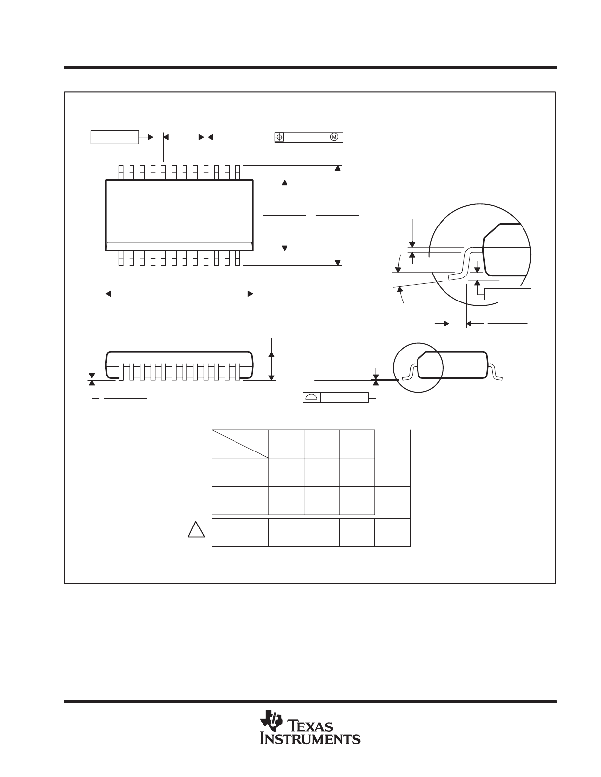
MSOI004E JANUARY 1995 − REVISED MAY 2002
DBQ (R−PDSO−G**) PLASTIC SMALL−OUTLINE PACKAGE
0.025 (0,64)
24
112
A
0.010 (0,25)
0.004 (0,10)
0.012 (0,30)
0.008 (0,20)
13
0.157 (3,99)
0.150 (3,81)
0.069 (1,75) MAX
0.005 (0,13)
0.244 (6,20)
0.228 (5,80)
Seating Plane
0.004 (0,10)
0.008 (0,20) NOM
Gauge Plane
0.010 (0,25)
0°−8°
0.035 (0,89)
0.016 (0,40)
PINS **
DIM
A MAX
A MIN
D
NOTES: A. All linear dimensions are in inches (millimeters).
B. This drawing is subject to change without notice.
C. Body dimensions do not include mold flash or protrusion not to exceed 0.006 (0,15).
D. Falls within JEDEC MO−137.
M0−137
VARIATION
16
0.197
(5,00)
0.189
(4,80)
AB AD AE AF
20 24
0.344
(8,74)
0.337
(8,56)
0.344
(8,74)
0.337
(8,56)
28
0.394
(10,01)
0.386
(9,80)
4073301/F 02/2002
POST OFFICE BOX 655303 • DALLAS, TEXAS 75265
1
Page 33

IMPORTANT NOTICE
Texas Instruments Incorporated and its subsidiaries (TI) reserve the right to make corrections, modifications,
enhancements, improvements, and other changes to its products and services at any time and to discontinue
any product or service without notice. Customers should obtain the latest relevant information before placing
orders and should verify that such information is current and complete. All products are sold subject to TI’s terms
and conditions of sale supplied at the time of order acknowledgment.
TI warrants performance of its hardware products to the specifications applicable at the time of sale in
accordance with TI’s standard warranty. Testing and other quality control techniques are used to the extent TI
deems necessary to support this warranty . Except where mandated by government requirements, testing of all
parameters of each product is not necessarily performed.
TI assumes no liability for applications assistance or customer product design. Customers are responsible for
their products and applications using TI components. To minimize the risks associated with customer products
and applications, customers should provide adequate design and operating safeguards.
TI does not warrant or represent that any license, either express or implied, is granted under any TI patent right,
copyright, mask work right, or other TI intellectual property right relating to any combination, machine, or process
in which TI products or services are used. Information published by TI regarding third-party products or services
does not constitute a license from TI to use such products or services or a warranty or endorsement thereof.
Use of such information may require a license from a third party under the patents or other intellectual property
of the third party, or a license from TI under the patents or other intellectual property of TI.
Reproduction of information in TI data books or data sheets is permissible only if reproduction is without
alteration and is accompanied by all associated warranties, conditions, limitations, and notices. Reproduction
of this information with alteration is an unfair and deceptive business practice. TI is not responsible or liable for
such altered documentation.
Resale of TI products or services with statements different from or beyond the parameters stated by TI for that
product or service voids all express and any implied warranties for the associated TI product or service and
is an unfair and deceptive business practice. TI is not responsible or liable for any such statements.
Following are URLs where you can obtain information on other Texas Instruments products and application
solutions:
Products Applications
Amplifiers amplifier.ti.com Audio www.ti.com/audio
Data Converters dataconverter.ti.com Automotive www.ti.com/automotive
DSP dsp.ti.com Broadband www.ti.com/broadband
Interface interface.ti.com Digital Control www.ti.com/digitalcontrol
Logic logic.ti.com Military www.ti.com/military
Power Mgmt power.ti.com Optical Networking www.ti.com/opticalnetwork
Microcontrollers microcontroller.ti.com Security www.ti.com/security
Telephony www.ti.com/telephony
Video & Imaging www.ti.com/video
Wireless www.ti.com/wireless
Mailing Address: Texas Instruments
Post Office Box 655303 Dallas, Texas 75265
Copyright 2004, Texas Instruments Incorporated
 Loading...