

Page 1
查询PCM1748供应商
Enhanced Multilevel, Delta-Sigma, Audio
PCM1748
PCM1748
SBAS165A – MAY 2001
24-Bit, 96kHz Sampling
DIGITAL-TO-ANALOG CONVERTER
FEATURES
●
24-BIT RESOLUTION
●
ANALOG PERFORMANCE (VCC = +5V):
Dynamic Range: 106dB typ (PCM1748KE)
100dB typ (PCM1748E)
SNR: 106dB typ (PCM1748KE)
100dB typ (PCM1748E)
THD+N: 0.002% typ (PCM1748KE)
0.003% typ (PCM1748E)
Full-Scale Output: 3.1Vp-p typ
●
8x OVERSAMPLING DIGITAL FILTER:
Stopband Attenuation: –55dB
Passband Ripple: ±0.03dB
●
SAMPLING FREQUENCY: 5kHz to 100kHz
●
SYSTEM CLOCK: 256, 384, 512, 768fS with
Auto Detect
●
ACCEPTS 16-, 18-, 20-, AND 24-BIT AUDIO
DATAzx
●
DATA FORMATS: Standard, I2S, and
Left-Justified
● USER-PROGRAMMABLE MODE CONTROLS:
Digital Attenuation: 0dB to –63dB, 0.5dB/Step
Digital De-Emphasis
Digital Filter Roll-Off: Sharp or Slow
Soft Mute
Zero Flags for Each Output
●
DUAL-SUPPLY OPERATION:
+5V Analog, +3.3V Digital
●
5V TOLERANT DIGITAL INPUTS
●
SMALL SSOP-16 PACKAGE
●
SAME PACKAGE SIZE AS SOP-8
APPLICATIONS
● A/V RECEIVERS
● DVD MOVIE PLAYERS
● DVD ADD-ON CARDS FOR HIGH-END PCs
● HDTV RECEIVERS
● CAR AUDIO SYSTEMS
● OTHER MULTICHANNEL AUDIO SYSTEMS
DESCRIPTION
The PCM1748 is a CMOS, monolithic, integrated circuit which
includes stereo Digital-to-Analog Converters (DACs) and support
circuitry in a small SSOP-16 package. The data converters utilize
Texas Instrument’s enhanced multilevel delta-sigma architecture
that employs fourth-order noise shaping and 8-level amplitude
quantization to achieve excellent dynamic performance and improved tolerance to clock jitter. The PCM1748 accepts industry
standard audio data formats with 16- to 24-bit data, providing easy
interfacing to audio DSP and decoder chips. Sampling rates up to
100kHz are supported. A full set of user-programmable functions
are accessible through a 3-wire serial control port that supports
register write functions.
Please be aware that an important notice concerning availability, standard warranty, and use in critical applications of
Texas Instruments semiconductor products and disclaimers thereto appears at the end of this data sheet.
PRODUCTION DATA information is current as of publication date.
Products conform to specifications per the terms of Texas Instruments
standard warranty. Production processing does not necessarily include
testing of all parameters.
Copyright © 2000, Texas Instruments Incorporated
www.ti.com
Page 2
ABSOLUTE MAXIMUM RATINGS
Power Supply Voltage, VDD.............................................................. +4.0V
Ground Voltage Differences..............................................................±0.1V
Digital Input Voltage................................................–0.3V to (6.5V + 0.3V)
Input Current (except power supply)............................................... ±10mA
Ambient Temperature Under Bias .................................. –40°C to +125°C
Storage Temperature...................................................... –55°C to +150°C
Junction Temperature .................................................................... +150°C
Lead Temperature (soldering, 5s)................................................. +260°C
Package Temperature (IR reflow, 10s) .......................................... +235°C
.............................................................. +6.5V
V
CC
This integrated circuit can be damaged by ESD. Texas Instruments recommends that all integrated circuits be handled with
appropriate precautions. Failure to observe proper handling
and installation procedures can cause damage.
ESD damage can range from subtle performance degradation
to complete device failure. Precision integrated circuits may
ELECTROSTATIC
DISCHARGE SENSITIVITY
be more susceptible to damage because very small parametric
changes could cause the device not to meet its published
specifications.
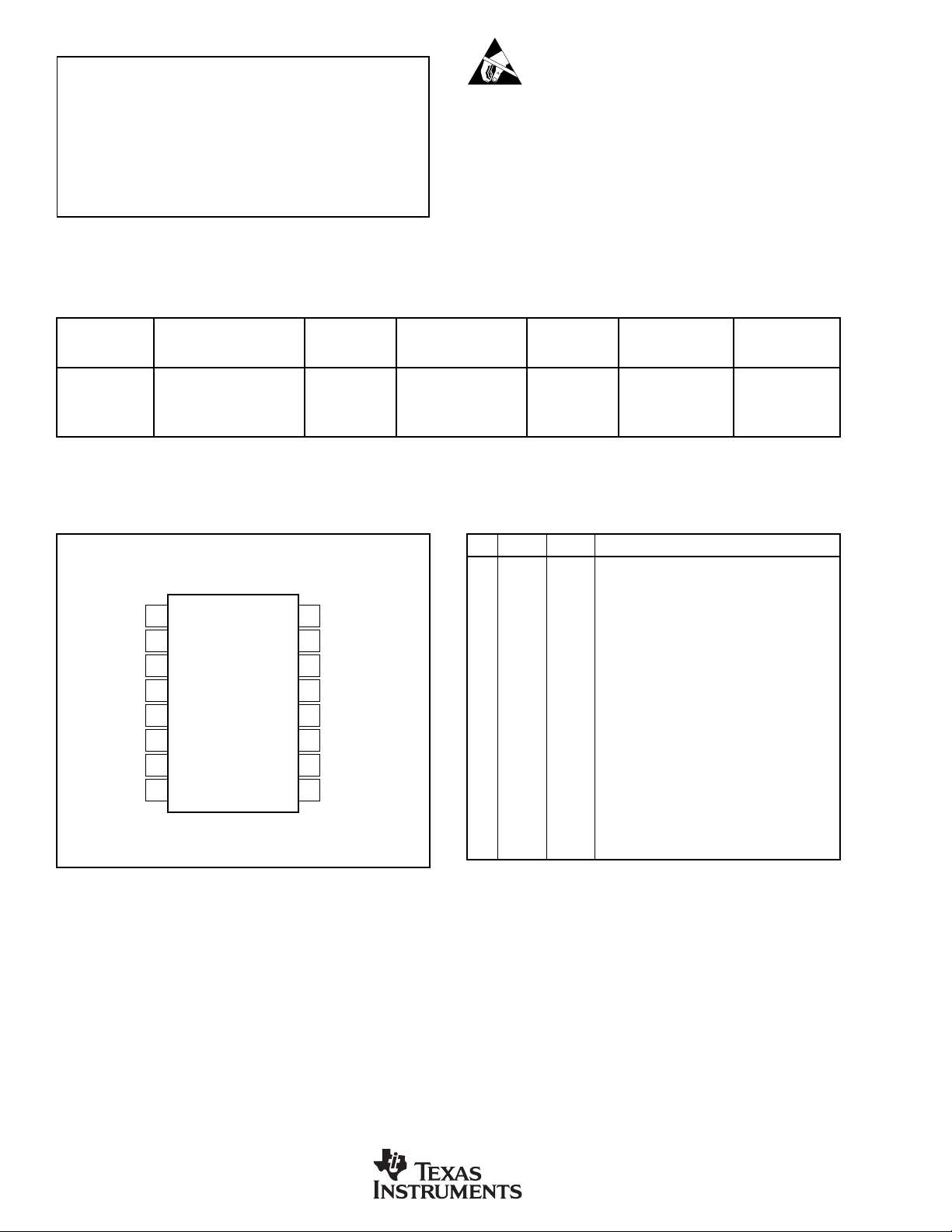
PACKAGE/ORDERING INFORMATION
PACKAGE SPECIFIED
PRODUCT PACKAGE NUMBER RANGE MARKING NUMBER
DRAWING TEMPERATURE PACKAGE ORDERING TRANSPORT
PCM1748E SSOP-16 322 –25°C to +85°C PCM1748E PCM1748E Rails
"""""PCM1748E/2K Tape and Reel
PCM1748KE SSOP-16 322 –25°C to +85°C PCM1748KE PCM1748KE Rails
"""""PCM1748KE/2K Tape and Reel
NOTE: (1) Models with a slash (/) are available only in Tape and Reel in the quantities indicated (e.g., /2K indicates 2000 devices per reel). Ordering 2000 pieces
of “PCM1748E/2K” will yield a single 2000-piece Tape and Reel.
(1)
MEDIA
PIN CONFIGURATION
TOP VIEW SSOP
BCK
DATA
LRCK
DGND
V
V
V
OUT
V
OUT
1
2
3
4
5
DD
6
CC
7
L
8
R
PCM1748
16
SCK
15
ML
14
MC
13
MD
12
ZEROL/NA
11
ZEROR/ZEROA
10
V
COM
9
AGND
PIN ASSIGNMENTS
PIN NAME TYPE FUNCTION
1 BCK IN Audio Data Bit Clock Input.
2 DATA IN Audio Data Digital Input.
3 LRCK IN L-Channel and R-Channel Audio Data Latch En-
4 DGND – Digital Ground
5VDD– Digital Power Supply, +3.3V
6V
CC
7V
8V
9 AGND – Analog Ground
10 V
11 ZEROR/ OUT Zero Flag Output for R-Channel/Zero Flag Output
12
13 MD IN Mode Control Data Input.
14 MC IN Mode Control Clock Input.
15 ML IN Mode Control Latch Input.
16 SCK IN System Clock Input.
NOTES: (1) Schmitt-trigger input, 5V tolerant. (2) Schmitt-trigger with internal
pull-down, 5V tolerant.
L OUT Analog Output for L-Channel.
OUT
R OUT Analog Output for R-Channel.
OUT
COM
ZEROA for L/R-Channel.
ZEROL/NA
able Input.
– Analog Power Supply, +5V
– Common Voltage Decoupling.
OUT Zero Flag Output for L-Channel/No Assign.
(1)
(1)
(1)
(2)
(2)
(2)
2
PCM1748
SBAS165
Page 3
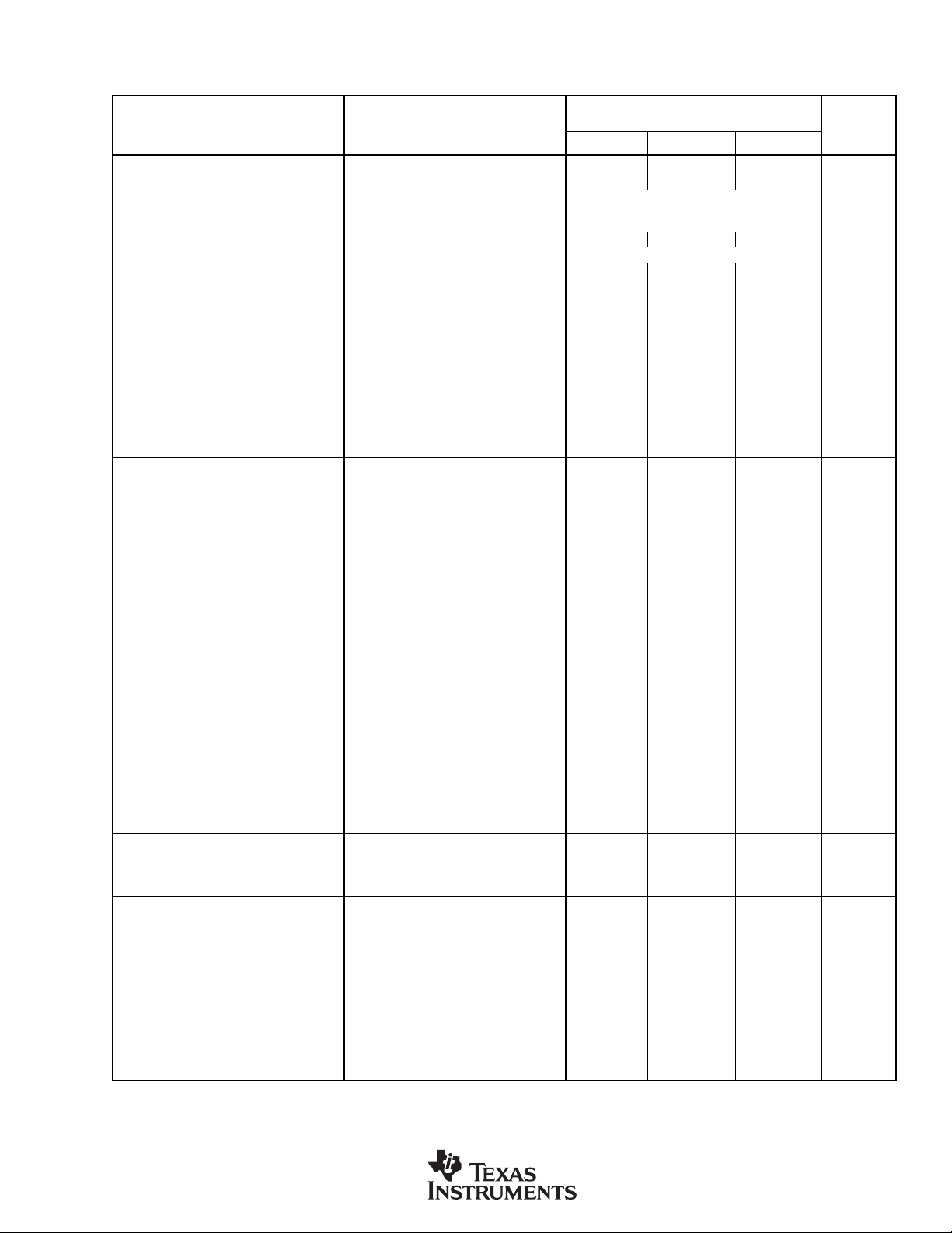
ELECTRICAL CHARACTERISTICS
All specifications at TA = +25°C, VCC = 5.0V, V
PARAMETER CONDITIONS MIN TYP MAX UNITS
RESOLUTION 24 Bits
DATA FORMAT
Audio Data Interface Formats Standard, IIS, Left-Justified
Audio Data Bit Length 16-, 18-, 20-, 24-Bits Selectable
Audio Data Format MSB-First, Binary Two’s Complement
Sampling Frequency (f
System Clock Frequency 256, 384, 512, 768f
) 5 100 kHz
S
DIGITAL INPUT/OUTPUT
Logic Family TTL-Compatible
Input Logic Level
V
IH
V
IL
Input Logic Current
(1)
I
IH
(1)
I
IL
(2)
I
IH
(2)
I
IL
Output Logic Level
(3)
V
OH
(3)
V
OL
DYNAMIC PERFORMANCE
(4)
PCM1748E
THD+N at V
THD+N at V
= 0dB fS = 44.1kHz 0.003 0.008 %
OUT
= –60dB fS = 44.1kHz 1.2 %
OUT
Dynamic Range EIAJ, A-Weighted, f
Signal-to-Noise Ratio EIAJ, A-Weighted, f
Channel Separation f
Level Linearity Error V
PCM1748KE
THD+N at V
THD+N at V
= 0dB fS = 44.1kHz 0.002 0.006 %
OUT
= –60dB fS = 44.1kHz 0.65 %
OUT
Dynamic Range EIAJ, A-Weighted, f
Signal-to-Noise Ratio EIAJ, A-Weighted, f
Channel Separation f
Level Linearity Error V
DC ACCURACY
Gain Error ±1.0 ±6 % of FSR
Gain Mismatch, Channel-to-Channel ±1.0 ±3 % of FSR
Bipolar Zero Error V
ANALOG OUTPUT
Output Voltage Full Scale (0dB) 62% of V
Center Voltage 50% V
Load Impedance AC Load 5 kΩ
DIGITAL FILTER PERFORMANCE
Filter Characteristics 1, Sharp Roll-Off
Passband ±0.03dB 0.454f
Passband –3dB 0.487f
Stopband 0.546f
Passband Ripple ±0.03 dB
Stopband Attenuation Stopband = 0.546f
Stopband Attenuation Stopband = 0.567f
= 3.3V, fS = 44.1kHz, system clock = 384fS, and 24-bit data, unless otherwise noted.
DD
PCM1748E
PCM1748KE
2.0 VDC
VIN = V
DD
VIN = 0V –10 µA
VIN = V
DD
VIN = 0V –10 µA
I
= –2mA 2.4 VDC
OH
I
= +2mA 1.0 VDC
OL
= 96kHz 0.004 %
f
S
= 96kHz 1.6 %
f
S
A-Weighted, f
A-Weighted, f
= 44.1kHz 91 98 dB
S
f
S
OUT
f
S
f
S
A-Weighted, f
A-Weighted, f
= 44.1kHz 97 103 dB
S
f
S
OUT
= 0.5 VCC at Bipolar Zero ±30 ±60 mV
OUT
= 44.1kHz 94 100 dB
S
= 96kHz 98 dB
S
= 44.1kHz 94 100 dB
S
= 96kHz 98 dB
S
= 96kHz 96 dB
= –90dB ±0.5 dB
= 96kHz 0.003 %
= 96kHz 0.8 %
= 44.1kHz 100 106 dB
S
= 96kHz 104 dB
S
= 44.1kHz 100 106 dB
S
= 96kHz 104 dB
S
= 96kHz 101 dB
= –90dB ±0.5 dB
S
S
S
–50 dB
–55
65 100 µA
CC
CC
S
0.8 VDC
10 µA
Vp-p
VDC
S
S
dB
PCM1748
SBAS165
3
Page 4
ELECTRICAL CHARACTERISTICS (Cont.)
All specifications at TA = +25°C, VCC = 5.0V, V
PARAMETER CONDITIONS MIN TYP MAX UNITS
DIGITAL FILTER PERFORMANCE (Cont.)
Filter Characteristics 2, Slow Roll-Off
Passband ±0.5dB 0.198f
Passband –3dB 0.390f
Stopband 0.884f
Passband Ripple ±0.5 d B
Stopband Attenuation Stopband = 0.884f
Delay Time 20/f
De-Emphasis Error ±0.1 dB
ANALOG FILTER PERFORMANCE
Frequency Response f = 20kHz –0.03 dB
POWER SUPPLY REQUIREMENTS
Voltage Range, V
Supply Current, I
DD
V
CC
(6)
DD
I
CC
(4)
Power Dissipation f
TEMPERATURE RANGE
Operation Temperature –25 +85 °C
Storage Temperature –55 +125 °C
Thermal Resistance
NOTES: (1) Pins 16, 1, 2, 3 (SCK, BCK, LRCK, DATA). (2) Pins 13-15 (MD, MC, ML). (3) Pins 11, 12 (ZEROR, ZEROL). (4) Analog performance specifications
are tested with a Shibasoku #725 THD Meter with 400Hz HPF on, 30kHz LPF on, and an average mode with 20kHz bandwidth limiting. The load connected
to the analog output is 5kΩ or larger, via capacitive coupling.
= 3.3V, system clock = 384fS (fS = 44.1kHz), and 24-bit data, unless otherwise noted.
DD
PCM1748E
PCM1748KE
S
S
–40 dB
f = 44kHz –0.20 dB
+3.0 +3.3 +3.6 VDC
+4.5 +5.0 +5.5 VDC
fS = 44.1kHz 6.0 10 mA
= 96kHz 13 mA
f
S
fS = 44.1kHz 8.5 13 mA
f
= 96kHz 9.0 mA
S
= 44.1kHz 62 98 mW
S
= 96kHz 88 mW
f
S
θ
JA
SSOP-16 115 °C/W
S
S
S
sec
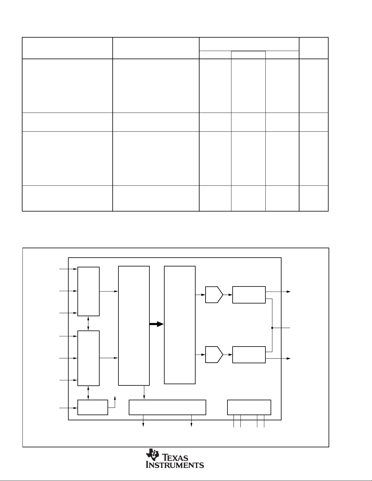
BLOCK DIAGRAM
BCK
LRCK
DATA
ML
MC
MD
SCK
Serial
Input
I/F
Function
Control
I/F
System Clock
Manager
Oversampling
Digital Filter
System Clock
8x
with
Function
Controller
Enhanced
Multi-Level
Delta-Sigma
Modulator
Zero Detect
DAC
DAC
Output Amp and
Low-Pass Filter
Output Amp and
Low-Pass Filter
Power Supply
V
L
OUT
V
COM
V
R
OUT
DD
V
ZEROL
ZEROR
4
DGND
V
CC
AGND
PCM1748
SBAS165
Page 5
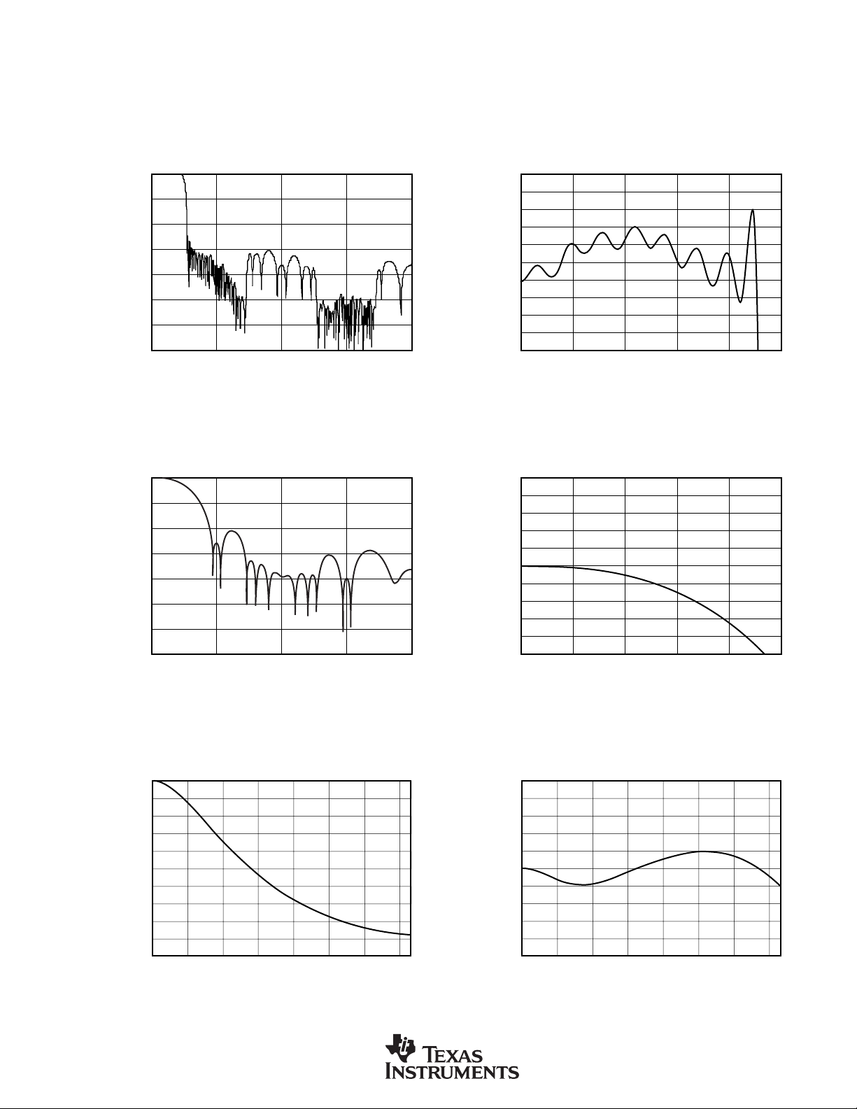
TYPICAL CHARACTERISTICS
5
4
3
2
1
0
–1
–2
–3
–4
–5
TRANSITION CHARACTERISTICS (Slow Roll-Off)
0 0.1 0.2 0.3 0.4 0.5
Frequency (x f
S
)
Amplitude (dB)
0.05
0.04
0.03
0.02
0.01
0
–0.01
–0.02
–0.03
–0.04
–0.05
FREQUENCY RESPONSE PASSBAND
(Sharp Roll-Off)
0 0.1 0.2 0.3 0.4 0.5
Frequency (x f
S
)
Amplitude (dB)
0.5
0.4
0.3
0.2
0.1
0.0
–0.1
–0.2
–0.3
–0.4
–0.5
DE-EMPHASIS ERROR (f
S
= 32kHz)
02468101214
Frequency (kHz)
Error (dB)
All specifications at TA = +25°C, VCC = 5.0V, VDD = 3.3V, system clock = 384fS (fS = 44.1kHz), and 24-bit input data, unless otherwise noted.
DIGITAL FILTER
Digital Filter (De-Emphasis Off, fS = 44.1kHz)
0
–20
–40
–60
–80
Amplitude (dB)
–100
–120
–140
0
–20
–40
–60
FREQUENCY RESPONSE (Sharp Roll-Off)
01234
Frequency (x f
FREQUENCY RESPONSE (Slow Roll-Off)
)
S
–80
Amplitude (dB)
–100
–120
–140
01234
De-Emphasis and De-Emphasis Error
0.0
–1.0
–2.0
–3.0
–4.0
–5.0
PCM1748
–6.0
Level (dB)
–7.0
–8.0
–9.0
–10.0
02468101214
SBAS165
DE-EMPHASIS (f
Frequency (x f
= 32kHz)
S
Frequency (kHz)
)
S
5
Page 6
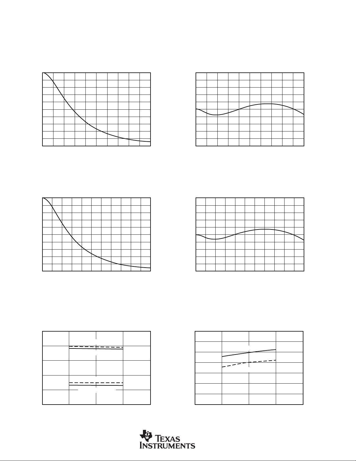
TYPICAL CHARACTERISTICS (Cont.)
All specifications at TA = +25°C, VCC = 5.0V, VDD = 3.3V, system clock = 384fS (fS = 44.1kHz), and 24-bit input data, unless otherwise noted.
De-Emphasis and De-Emphasis Error (Cont.)
0.0
–1.0
–2.0
–3.0
–4.0
–5.0
–6.0
Level (dB)
–7.0
–8.0
–9.0
–10.0
02468101214161820
0.0
–1.0
–2.0
–3.0
–4.0
–5.0
–6.0
Level (dB)
–7.0
–8.0
–9.0
–10.0
02468101214
DE-EMPHASIS (f
Frequency (kHz)
DE-EMPHASIS (f
Frequency (kHz)
= 44.1kHz)
S
= 48kHz)
S
0.5
0.4
0.3
0.2
0.1
0.0
–0.1
Error (dB)
–0.2
–0.3
–0.4
–0.5
02468101214161820
0.5
0.4
0.3
0.2
0.1
0.0
–0.1
Error (dB)
–0.2
–0.3
–0.4
–0.5
18
16
2220
02468101214
DE-EMPHASIS ERROR (f
Frequency (kHz)
DE-EMPHASIS ERROR (f
Frequency (kHz)
= 44.1kHz)
S
= 48kHz)
S
16
18
2220
ANALOG DYNAMIC PERFORMANCE
All specifications at TA = +25°C, VCC = 5.0V, VDD = 3.3V, and 24-bit input data, unless otherwise noted.
Supply-Voltage Characteristics
(VDD = 3.3V)
CC
0dB/96kHz, 384f
0dB/44.1kHz, 384f
(V)
V
CC
110
S
S
108
106
104
102
S
S
SNR (dB)
100
98
96
4 4.5 5 5.5 6
0.1
0.01
THD+N (%)
0.001
0.0001
6
10
1
THD+N vs V
–60dB/96kHz, 384f
–60dB/44.1kHz, 384f
4 4.5 5 5.5 6
DYNAMIC RANGE vs V
44.1kHz, 384f
96kHz, 384f
S
(V)
V
CC
(VDD = 3.3V)
CC
S
PCM1748
SBAS165
Page 7
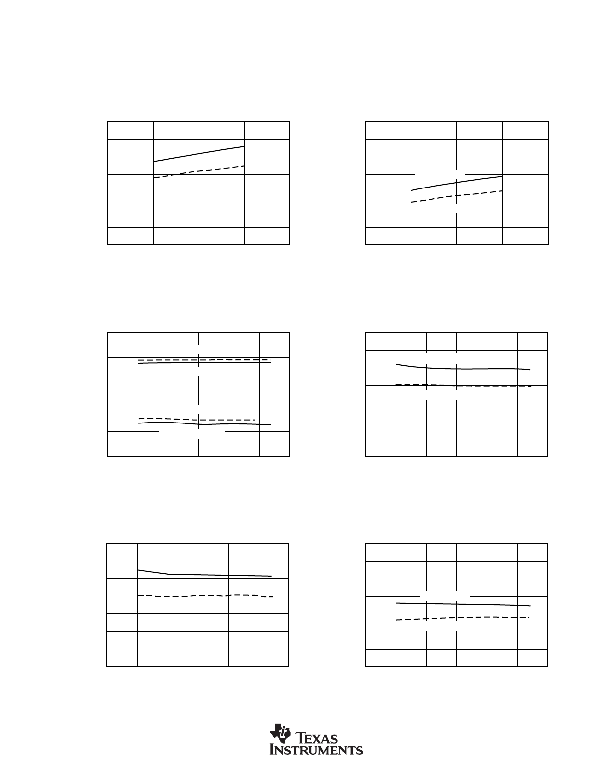
TYPICAL CHARACTERISTICS (Cont.)
110
108
106
104
102
100
98
96
CHANNEL SEPARATION vs V
CC
(VDD = 3.3V)
4 4.5 5 5.5 6
V
CC
(V)
Channel Separation (dB)
44.1kHz, 384f
S
96kHz, 384f
S
110
108
106
104
102
100
98
96
DYNAMIC RANGE vs T
A
–50 –25 0 25 50 75 100
Temperature (°C)
Dynamic Range (dB)
44.1kHz, 384f
S
96kHz, 384f
S
All specifications at TA = +25°C, VCC = 5.0V, VDD = 3.3V, and 24-bit input data, unless otherwise noted.
Supply-Voltage Characteristics (Cont.)
110
SNR vs V
(VDD = 3.3V)
CC
108
106
104
96kHz, 384f
102
SNR (dB)
100
98
96
4 4.5 5 5.5 6
V
CC
Temperature Characteristics
10
1
0.1
THD+N vs T
–60dB/96kHz, 384f
–60dB/44.1kHz, 384f
S
(V)
A
S
S
0.01
THD+N (%)
0.001
0dB/96kHz, 384f
0dB/44.1kHz, 384f
0.0001
–50 –25 0 25 50 75 100
110
108
106
104
102
SNR (dB)
100
98
96
–50 –25 0 25 50 75 100
PCM1748
SBAS165
S
Temperature (°C)
SNR vs T
A
44.1kHz, 384f
96kHz, 384f
S
Temperature (°C)
S
110
CHANNEL SEPARATION vs T
A
108
S
106
104
44.1kHz, 384f
S
102
100
Channel Separation (dB)
98
96kHz, 384f
S
96
–50 –25 0 25 50 75 100
Temperature (°C)
7
Page 8

SYSTEM CLOCK AND RESET
FUNCTIONS
SYSTEM CLOCK INPUT
The PCM1748 requires a system clock for operating the
digital interpolation filters and multilevel delta-sigma modulators. The system clock is applied at the SCK input (pin 16).
Table I shows examples of system clock frequencies for
common audio sampling rates.
Figure 1 shows the timing requirements for the system clock
input. For optimal performance, it is important to use a clock
source with low phase jitter and noise. The PLL1700 multiclock generator from Texas Instruments is an excellent choice
for providing the PCM1748 system clock.
POWER-ON RESET FUNCTIONS
The PCM1748 includes a power-on reset function, as shown in
Figure 2. With the system clock active, and VDD > 2.0V (typical
1.6V to 2.4V), the power-on reset function will be enabled.
After the initialization period, the PCM1748 will be set to its
reset default state, as described in the Mode Control Register
section of this data sheet.
During the reset period, the analog outputs are forced to the
bipolar zero level, or VCC/2. After the reset period, the
internal register is initialized in the next 1/fS period and, if
SCK, BCK, and LRCK are provided continuously, the
PCM1748 provides proper analog output with unit group
delay against the input data.
SAMPLING
FREQUENCY 256f
8kHz 2.0480 3.0720 4.0960 6.1440
16kHz 4.0960 6.1440 8.1920 12.2880
32kHz 8.1920 12.2880 16.3840 24.5760
44.1kHz 11.2896 16.9344 22.5792 33.8688
48kHz 12.2880 18.4320 24.5760 36.8640
88.2kHz 22.5792 33.8688 45.1584 See Note (1)
96kHz 24.5760 36.8640 49.1520 See Note (1)
NOTE: (1) The 768fS system clock rate is not supported for fS > 64kHz.
S
SYSTEM CLOCK FREQUENCY (f
384f
S
TABLE I. System Clock Rates for Common Audio Sampling Frequencies.
t
SCKH
“H”
System Clock
“L”
t
SCKL
System Clock Pulse Width HIGH t
System Clock Pulse Width LOW t
NOTE: (1) 1/256fS, 1/384fS, 1/512fS, or 1/768fS.
System clock pulse
cycle time
SCKH
SCKL
(1)
: 7ns (min)
: 7ns (min)
SCLK
512f
) (MHz)
S
2.0V
0.8V
768f
S
FIGURE 1. System Clock Input Timing.
V
Internal Reset
System Clock
2.4V
2.0V
DD
1.6V
0V
Don't Care
FIGURE 2. Power-On Reset Timing.
8
Reset Reset Removal
1024 System Clocks
PCM1748
SBAS165
Page 9

AUDIO SERIAL INTERFACE
The audio serial interface for the PCM1748 is comprised of
a 3-wire synchronous serial port. It includes LRCK (pin 3),
BCK (pin 1), and DATA (pin 2). BCK is the serial audio bit
clock, and is used to clock the serial data present on DATA
into the audio interface’s serial shift register. Serial data is
clocked into the PCM1748 on the rising edge of BCK.
LRCK is the serial audio left/right word clock used to latch
serial data into the serial audio interface’s internal registers.
Both LRCK and BCK should be synchronous to the
system clock. Ideally, it is recommended that LRCK and
BCK be derived from the system clock input, SCK. LRCK
is operated at the sampling frequency, fS. BCK may be
operated at 32, 48, or 64 times the sampling frequency.
Internal operation of the PCM1748 is synchronized with
LRCK. Accordingly, it is held when the sampling rate
clock of LRCK is changed or SCK and/or BCK is broken at
least for one clock cycle. If SCK, BCK, and LRCK are
provided continuously after this hold condition, the internal
operation will be resynchronized automatically, less than 3/f
period. In this resynchronize period, and following 3/fS,
analog output is forced to the bipolar zero level, or
VCC/2.
External resetting is not required.
AUDIO DATA FORMATS AND TIMING
The PCM1748 supports industry-standard audio data formats,
including Standard, I
2
S, and Left-Justified, as shown in
Figure 3. Data formats are selected using the format bits,
FMT[2:0], in Control Register 20. The default data format is
24-bit left justified. All formats require Binary Two’s Complement, MSB-first audio data. See Figure 4 for a detailed timing
diagram of the serial audio interface.
S
(1) Standard Data Format: L-Channel = HIGH, R-Channel = LOW
LRCK
BCK
or 64fS)
(= 32, 48
16-Bit Right-Justified, BCK = 48fS or 64f
16-Bit Right-Justified, BCK = 32f
18-Bit Right-Justified
20-Bit Right-Justified
24-Bit Right-Justified
DATA
14 15 16
DATA
14 15 16 14 15 16123
DATA
16 17 18
18 19 20
DATA
DATA
22 23 24 22 23 24123
S
S
L-Channel
123
14 15 16
16 17 181 23
18 19 201 23
(2) I2S Data Format: L-Channel = LOW, R-Channel = HIGH
LRCK
BCK
(= 48 or 64f
DATA
)
S
1 2 3
L-Channel
N-2 N-1 N
1/f
S
LSBMSB
LSBMSB LSBMSB
LSBMSB
LSBMSB
LSBMSB
1/f
S
1 2 1 23
R-Channel
14 15 16123
LSBMSB
14 15 16123
17 181 2
LSBMSB
18 19 201 23
LSBMSB
22 23 24123
LSBMSB
R-Channel
N-2 N-1 N
(3) Left-Justified Data Format: L-Channel = HIGH, R-Channel = LOW
LRCK
BCK
(= 32, 48 or 64f
S
DATA
)
1 2 3
FIGURE 3. Audio Data Input Formats.
PCM1748
SBAS165
L-Channel
N-2 N-1 N
LSBMSB LSBMSB
1/f
S
1 2 3
R-Channel
N-2 N-1 N
LSBMSBLSBMSB
21
9
Page 10

LRCK
BCK
t
BCH
t
BCY
50% of V
DD
t
BCL
t
BL
t
LB
50% of V
DD
DATA
t
DS
SYMBOL PARAMETER MIN MAX UNITS
t
BCY
t
BCH
t
BCL
t
BL
t
LB
t
DS
t
DH
NOTE: (1) f
is the sampling frequency (e.g., 44.1kHz, 48kHz, 96kHz, etc.)
S
BCK Pulse Cycle Time
BCK High Level Time 35 ns
BCK Low Level Time 35 ns
BCK Rising Edge to LRCK Edge 10 ns
LRCK Falling Edge to BCK Rising Edge 10 ns
DATA Set Up Time 10 ns
DATA Hold Time 10 ns
t
DH
FIGURE 4. Audio Interface Timing.
SERIAL CONTROL INTERFACE
The serial control interface is a 3-wire serial port that
operates asynchronously to the serial audio interface. The
serial control interface is utilized to program the on-chip
mode registers. The control interface includes MD (pin 13),
MC (pin 14), and ML (pin 15). MD is the serial data input,
used to program the mode registers; MC is the serial bit
clock, used to shift data into the control port; and ML is the
control port latch clock.
REGISTER WRITE OPERATION
All Write operations for the serial control port use 16-bit
data words. Figure 5 shows the control data word format.
The most significant bit must be a “0”. There are seven bits,
labeled IDX[6:0], that set the register index (or address) for
50% of V
DD
32, 48, or 64f
(1)
S
the Write operation. The least significant eight bits, D[7:0],
contain the data to be written to the register specified by
IDX[6:0].
Figure 6 shows the functional timing diagram for writing the
serial control port. ML is held at a logic “1 ” state until a
register needs to be written. To start the register write cycle,
ML is set to logic “0”. Sixteen clocks are then provided on
MC, corresponding to the 16 bits of the control data word on
MD. After the sixteenth clock cycle has completed, ML is
set to logic “1” to latch the data into the indexed mode
control register.
CONTROL INTERFACE TIMING REQUIREMENTS
Figure 7 shows a detailed timing diagram for the serial
control interface. These timing parameters are critical for
proper control port operation.
MSB
IDX5IDX60 IDX4 IDX2IDX3 IDX1 IDX0 D7 D6 D5 D4 D3 D2 D1 D0
Register Index (or Address) Register Data
FIGURE 5. Control Data Word Format for MDI.
ML
MC
0D7D6D5D4D3D20
MDI
IDX6 IDX5 IDX4 IDX3 IDX2 IDX1 IDX0
FIGURE 6. Register Write Operation.
10
LSB
D1 D0X XX
IDX6
PCM1748
SBAS165
Page 11

MODE CONTROL REGISTERS
User-Programmable Mode Controls
The PCM1748 includes a number of user-programmable
functions that are accessed via control registers. The registers are programmed using the Serial Control Interface that
was previously discussed in this data sheet. Table II lists the
ML
t
MLS
t
MCH
t
MCL
available mode control functions, along with their reset
default conditions and associated register index.
Register Map
The mode control register map is shown in Table III. Each
register includes an index (or address) indicated by the
IDX[6:0] bits.
t
MHH
50% of V
DD
t
MLH
MC
MD
t
MCY
t
MDS
SYMBOL PARAMETER MIN TYP MAX UNITS
t
MCY
t
MCL
t
MCH
t
MHH
t
MLS
t
MLH
t
MDH
t
MDS
NOTES: (1) MC rising edge for LSB to ML rising edge. (2)
MC Pulse Cycle Time 100 ns
MC High Level Time 50 ns
ML High Level Time Note (2) ns
ML Falling Edge to MC Rising Edge 20 ns
t
MCH
MC Low Level Time 50 ns
ML Hold Time
MD Hold Time 15 ns
MD Set Up Time 20 ns
(1)
3
256 • F
LSB
20 ns
sec (min), FS = Sampling Rate.
S
50% of V
50% of V
FIGURE 7. Control Interface Timing.
FUNCTION RESET DEFAULT CONTROL REGISTER INDEX, IDX[6:0]
Digital Attenuation Control, 0dB to –63dB in 0.5dB Steps 0dB, No Attenuation 16 and 17 AT1[7:0], AT2[7:0]
Soft Mute Control Mute Disabled 18 MUT[2:0]
Oversampling Rate Control (64 or 128fS) 64fS Oversampling 18 OVER
DAC Operation Control DAC1 and DAC2 Enabled 19 DAC[2:1]
De-Emphasis Function Control De-Emphasis Disabled 19 DM12
De-Emphasis Sample Rate Selection 44.1kHz 19 DMF[1:0]
Audio Data Format Control 24-Bit Left Justified 20 FMT[2:0]
Digital Filter Roll-Off Control Sharp Roll-Off 20 FLT
Zero Flag Function Select L-/R-Channel Independent 22 AZRO
Output Phase Select Normal Phase 22 DREV
Zero Flag Polarity Select High 22 ZREV
DD
DD
TABLE II. User-Programmable Mode Controls.
IDX
(B8-B14) REGISTER B15 B14 B13 B12 B11 B10 B9 B8 B7 B6 B5 B4 B3 B2 B1 B0
10
H
11
H
12
H
13
H
14
H
15
H
16
H
16 0 IDX6 IDX5 IDX4 IDX3 IDX2 IDX1 IDX0 AT17 AT16 AT15 AT14 AT13 AT12 AT11 AT10
17 0 IDX6 IDX5 IDX4 IDX3 IDX2 IDX1 IDX0 AT27 AT26 AT25 AT24 AT23 AT22 AT21 AT20
18 0 IDX6 IDX5 IDX4 IDX3 IDX2 IDX1 IDX0 RSV OVER RSV RSV RSV RSV MUT2 MUT1
19 0 IDX6 IDX5 IDX4 IDX3 IDX2 IDX1 IDX0 RSV DMF1 DMF0 DM12 RSV RSV DAC2 DAC1
20 0 IDX6 IDX5 IDX4 IDX3 IDX2 IDX1 IDX0 RSV RSV FLT RSV RSV FMT2 FMT1 FMT0
21 0 IDX6 IDX5 IDX4 IDX3 IDX2 IDX1 IDX0 RSV RSV RSV RSV RSV RSV RSV RSV
22 0 IDX6 IDX5 IDX4 IDX3 IDX2 IDX1 IDX0 RSV RSV RSV RSV RSV AZRO ZREV DREV
TABLE III. Mode Control Register Map.
PCM1748
SBAS165
11
Page 12

REGISTER DEFINITIONS
B15 B14 B13 B12 B11 B10 B9 B8 B7 B6 B5 B4 B3 B2 B1 B0
Register 16 0 IDX6 IDX5 IDX4 IDX3 IDX2 IDX1 IDX0 AT17 AT16 AT15 AT14 AT13 AT12 AT11 AT10
Register 17 0 IDX6 IDX5 IDX4 IDX3 IDX2 IDX1 IDX0 AT27 AT26 AT25 AT24 AT23 AT22 AT21 AT20
ATx[7:0] Digital Attenuation Level Setting
where x = 1 or 2, corresponding to the DAC output V
Default Value: 1111 1111
Each DAC channel (V
OUT
B
L and V
R) includes a digital attenuator function. The attenuation level may be
OUT
L (x = 1) and V
OUT
R (x = 2).
OUT
set from 0dB to –63dB, in 0.5dB steps. The attenuation data for each channel can be set individually.
The attenuation level may be set using the formula below.
Attenuation Level (dB) = 0.5 (ATx[7:0]
where: ATx[7:0]
for: ATx[7:0]
= 0 through 255
DEC
= 0 through 128, the attenuator is set to infinite attenuation.
DEC
DEC
– 255)
The following table shows attenuator levels for various settings.
ATx[7:0] Decimal Value Attenuator Level Setting
1111 1111
1111 1110
1111 1101
1000 0011
1000 0010
1000 0001
1000 0000
B
B
B
B
B
B
B
255 0dB, No Attenuation (default)
254 –0.5dB
253 –1.0dB
131 –62.0dB
130 –62.5dB
129 –63.0dB
128 Mute
•••
•••
•••
0000 0000
Register 18 0 IDX6 IDX5 IDX4 IDX3 IDX2 IDX1 IDX0 RSV OVER RSV RSV RSV RSV MUT2 MUT1
B
B15 B14 B13 B12 B11 B10 B9 B8 B7 B6 B5 B4 B3 B2 B1 B0
0 Mute
MUTx Soft Mute Control
Where x = 1 or 2, corresponding to the DAC output V
L (x = 1) and V
OUT
R (x = 2).
OUT
Default Value: 0
MUTx = 0 Mute Disabled (default)
MUTx = 1 Mute Enabled
The mute bits, MUT1 and MUT2, are used to enable or disable the Soft Mute function for the corresponding
DAC outputs, V
OUT
L and V
R. The Soft Mute function is incorporated into the digital attenuators. When
OUT
Mute is disabled (MUTx = 0), the attenuator and DAC operate normally. When Mute is enabled by setting
MUTx = 1, the digital attenuator for the corresponding output will be decreased from the current setting
to the infinite attenuation setting one attenuator step (0.5dB) at a time. This provides a quiet, “pop”-free
muting of the DAC output.
OVER Oversampling Rate Control
Default Value: 0
OVER = 0 64x Oversampling (default)
OVER = 1 128x Oversampling
The OVER bit is used to control the oversampling rate of the delta-sigma DACs.
12
PCM1748
SBAS165
Page 13

B15 B14 B13 B12 B11 B10 B9 B8 B7 B6 B5 B4 B3 B2 B1 B0
REGISTER 19 0 IDX6 IDX5 IDX4 IDX3 IDX2 IDX1 IDX0 RSV DMF1 DMF0 DM12 RSV RSV DAC2 DAC1
DACx DAC Operation Control
where x = 1 or 2, corresponding to the DAC output V
L (x = 1) or V
OUT
R (x = 2).
OUT
Default Value: 0
DACx = 0 DAC Operation Enabled (default)
DACx = 1 DAC Operation Disabled
The DAC operation controls are used to enable and disable the DAC outputs, V
DACx = 0, the corresponding output will generate the audio waveform dictated by the data present on the
DATA pin. When DACx = 1, the corresponding output will be set to the bipolar zero level, or
DM12 Digital De-Emphasis Function Control
Default Value: 0
DM12 = 0 De-Emphasis Disabled (default)
DM12 = 1 De-Emphasis Enabled
The DM12 bit is used to enable or disable the Digital De-Emphasis function. Refer to the Typical Performance
Curves of this data sheet for more information.
DMF[1:0] Sampling Frequency Selection for the De-Emphasis Function
Default Value: 00
B
DMF[1:0] De-Emphasis Same Rate Selection
00 44.1kHz (default)
01 48kHz
10 32kHz
11 Reserved
The DMF[1:0] bits are used to select the sampling frequency used for the Digital De-Emphasis function when
it is enabled.
OUT
L and V
R. When
OUT
VCC/2.
B15 B14 B13 B12 B11 B10 B9 B8 B7 B6 B5 B4 B3 B2 B1 B0
REGISTER 20 0 IDX6 IDX5 IDX4 IDX3 IDX2 IDX1 IDX0 RSV RSV FLT RSV RSV FMT2 FMT1 FMT0
FMT[2:0] Audio Interface Data Format
Default Value: 000
B
The FMT[2:0] bits are used to select the data format for the serial audio interface. The following table shows
the available format options.
FMT[2:0] Audio Data Format Selection
000 24-Bit Standard Format, Right-Justified Data (default)
001 20-Bit Standard Format, Right-Justified Data
010 18-Bit Standard Format, Right-Justified Data
011 16-Bit Standard Format, Right-Justified Data
100 I2S Format, 16- to 24-bits
101 Left-Justified Format, 16- to 24-Bits
110 Reserved
111 Reserved
PCM1748
SBAS165
13
Page 14

Register 20 (Cont.)
FLT Digital Filter Roll-Off Control
Default Value: 0
FLT = 0 Sharp Roll-Off (default)
FLT = 1 Slow Roll-Off
The FLT bit allows the user to select the digital filter roll-off that is best suited to their application. Two
filter roll-off sections are available: Sharp or Slow. The filter responses for these selections are shown in
the Typical Performance Curves section of this data sheet.
B15 B14 B13 B12 B11 B10 B9 B8 B7 B6 B5 B4 B3 B2 B1 B0
REGISTER 22 0 IDX6 IDX5 IDX4 IDX3 IDX2 IDX1 IDX0 RSV RSV RSV RSV RSV AZRO ZREV DREV
DREV Output Phase Select
Default Value: 0
DREV = 0 Normal Output (default)
DREV = 1 Inverted Output
The DREV bit is used to set the output phase of V
ZREV Zero Flag Polarity Select
Default Value: 0
ZREV = 0 Zero Flag Pins HIGH at a Zero Detect (default)
ZREV = 1 Zero Flag Pins LOW at a Zero Detect
The ZREV bit allows the user to select the active polarity of Zero Flag pins.
AZRO Zero Flag Function Select
Default Value: 0
AZRO = 0 L-/R-Channel Independent Zero Flag (default)
AZRO = 1 L-/R-Channel Common Zero Flag
The AZRO bit allows the user to select the function of Zero Flag pins.
AZRO = 0:
Pin11: ZEROR; Zero Flag Output for R-Channel
Pin12: ZEROL; Zero Flag Output for L-Channel
AZRO = 1:
OUT
L and V
OUT
R.
14
Pin11: ZEROA; Zero Flag Output for L-/R-Channel
Pin12: NA; No Assign
PCM1748
SBAS165
Page 15

ANALOG OUTPUTS
The PCM1748 includes two independent output channels:
V
L and V
OUT
capable of driving 3.1Vp-p typical into a 5kΩ AC-coupled
load. The internal output amplifiers for V
are biased to the DC common-mode (or bipolar zero) voltage, equal to VCC/2.
The output amplifiers include an RC continuous-time filter
that helps to reduce the out-of-band noise energy present at
the DAC outputs, due to the noise shaping characteristics of
the PCM1748’s delta-sigma DACs. The frequency response
of this filter is shown in Figure 8. By itself, this filter is not
–10
–20
–30
Response (dB)
–40
–50
–60
FIGURE 8. Output Filter Frequency Response.
R. These are unbalanced outputs, each
OUT
L and V
OUT
ANALOG FILTER PERFORMANCE
(100Hz-10MHz)
0
0.1 1 10 100 1K 10K
Frequency (kHz)
OUT
enough to attenuate the out-of-band noise to an acceptable
level for many applications, therefore, an external low-pass
filter is required to provide sufficient out-of-band noise
rejection. Further discussion of DAC post-filter circuits is
provided in the Applications Information section of this data
R
sheet.
V
OUTPUT
COM
One unbuffered common-mode voltage output pin, V
COM
(pin 10), is brought out for decoupling purposes. This pin is
nominally biased to a DC voltage level equal to
VCC/2.
This
pin may be used to bias external circuits. An example of
using the V
pin for external biasing applications is
COM
shown in Figure 9.
ZERO FLAGS
Zero Detect Condition
Zero Detection for each output channel is independent from
the other. If the data for a given channel remains at a “0”
level for 1024 sample periods (or LRCK clock periods), a
Zero Detect condition exists for that channel.
Zero Output Flags
Given that a Zero Detect condition exists for one or more
channels, the Zero Flag pins for those channels will be set to
a logic “1” state. There are Zero Flag pins for each channel,
ZEROL (pin 12) and ZEROR (pin 11). These pins can be used
PCM1748
V
x
OUT
V
COM
x = L or R
(a) Using V
(b) Using a Voltage Follower to Buffer V
(c) Using an INA134 for DC-Coupled Output
to Bias a Single-Supply Filter Stage
COM
PCM1748
V
COM
PCM1748
V
x
OUT
V
COM
x = L or R
V
+
10µF
+
CC
+
+
49.9kΩ
1%
10µF
R
10µF
10µF
–IN
+IN
R
2
25kΩ
25kΩ
C
2
V
OPA337
R
3
CC
1
when Biasing Multiple Nodes
COM
V+
INA134
V–
25kΩ
25kΩ
C
1
2
OPA2353
3
Buffered
V
COM
SENSE
OUT
REF
R
V
CC
1/2
AV = –1, where AV = –
1
To Low-Pass
Filter Stage
Filtered
Output
2
R
1
FIGURE 9. Biasing External Circuits Using the V
PCM1748
SBAS165
COM
Pin.
15
Page 16

to operate external mute circuits, or used as status indicators
for a microcontroller, audio signal processor, or other digitally
controlled functions.
The active polarity of Zero Flag output can be inverted by
setting the ZREV bit of Control Register 22 to “1”. The reset
default is active high output, or ZREV = 0.
APPLICATIONS INFORMATION
Connection Diagrams
A basic connection diagram is shown in Figure 11, with the
necessary power-supply bypassing and decoupling components. Texas Instruments recommends using the component
values shown in Figure 11 for all designs.
R
2
AV ≈ –
R
R
2
R
V
1
IN
R
C
2
C
1
3
2
OPA2134
3
R
1
4
FIGURE 10. Dual-Supply Filter Circuit.
The use of series resistors (22Ω to 100Ω) are recommended
for the SCK, LRCK, BCK, and DATA inputs. The series
resistor combines with stray PCB and device input capacitance to form a low-pass filter that reduces high-frequency
noise emissions and helps to dampen glitches and ringing
present on clock and data lines.
1
V
OUT
Power Supplies and Grounding
The PCM1748 requires a +5V analog supply and a +3.3V
digital supply. The +5V supply is used to power the DAC
analog and output filter circuitry, while the +3.3V supply is
used to power the digital filter and serial interface circuitry.
For best performance, the +3.3V supply should be derived
from the +5V supply using a linear regulator, as shown in
Figure 11. The REG1117-3.3 from Texas Instruments is an
ideal choice for this application.
Proper power-supply bypassing is shown in Figure 11. The
10µF capacitors should be tantalum or aluminum electrolytic.
DAC Output Filter Circuits
Delta-sigma DACs utilize noise-shaping techniques to improve in-band Signal-to-Noise Ratio (SNR) performance at
the expense of generating increased out-of-band noise above
the Nyquist Frequency, or f
/2. The out-of-band noise must
S
be low-pass filtered in order to provide the optimal converter
performance. This is accomplished by a combination of
on-chip and external low-pass filtering.
Figures 9(a) and 10 show the recommended external lowpass active filter circuits for single- and dual-supply applications. These circuits are second-order Butterworth filters
using the Multiple FeedBack (MFB) circuit arrangement
that reduces sensitivity to passive component variations over
frequency and temperature. For more information regarding
MFB active filter design, please refer to Burr-Brown Applications Bulletin #34 (AB-034), available from our web site
at http://www.ti.com.
Since the overall system performance is defined by the
quality of the DACs and their associated analog output
circuitry, high-quality audio op amps are recommended for
the active filters. The OPA2353 and OPA2134 dual op amps
from Texas Instruments are recommended for use with the
PCM1748, see Figures 9(a) and 10.
PCM
Audio Data
Input
+3.3V
Regulator
+5V V
CC
FIGURE 11. Basic Connection Diagram.
16
+
10µF
+
10µF
Post LPF
L-Chan OUT
Post LPF
System Clock
Mode
Control
Zero Mute
Control
+
10µF
1
BCK
DATA
2
LRCK
3
DGND
4
V
5
DD
6
V
CC
7
V
L
OUT
8
V
R
OUT
ZEROR/ZEROA
SCK
ML
MC
MDI
ZEROL/NA
V
COM
AGND
16
15
14
13
12
11
10
9
R-Chan OUT
PCM1748
SBAS165
Page 17

PCB LAYOUT GUIDELINES
A typical PCB floor plan for the PCM1748 is shown in
Figure 12. A ground plane is recommended, with the analog
and digital sections being isolated from one another using a
split or cut in the circuit board. The PCM1748 should be
oriented with the digital I/O pins facing the ground plane
split/cut to allow for short, direct connections to the digital
audio interface and control signals originating from the
digital section of the board.
Separate power supplies are recommended for the digital and
analog sections of the board. This prevents the switching noise
present on the digital supply from contaminating the analog
power supply and degrading the dynamic performance of the
PCM1748. In cases where a common +5V supply must be
used for the analog and digital sections, an inductance (RF
choke, ferrite bead) should be placed between the analog and
digital +5V supply connections to avoid coupling of the digital
switching noise into the analog circuitry. Figure 13 shows the
recommended approach for single-supply applications.
Digital Power
+V
DGND
D
Digital Logic
and
Audio
Processor
DIGITAL SECTION ANALOG SECTION
FIGURE 12. Recommended PCB Layout.
Analog Power
+5VA +V
AGND
REG
V
DD
DGND
Return Path for Digital Signals
V
PCM1748
AGND
–V
S
S
CC
Output
Circuits
Digital
Ground
Analog
Ground
RF Choke or Ferrite Bead
V
DD
DIGITAL SECTION ANALOG SECTION
FIGURE 13. Single-Supply PCB Layout.
PCM1748
SBAS165
Power Supplies
+5V +V
AGND
REG
V
CC
V
DD
DGND
PCM1748
AGND
–V
S
S
Output
Circuits
Common
Ground
17
Page 18

THEORY OF OPERATION
The delta-sigma section of the PCM1748 is based on an
8-level amplitude quantizer and a fourth-order noise shaper. This
section converts the oversampled input data to 8-level delta-sigma
format. A block diagram of the 8-level delta-sigma modulator is
shown in Figure 14. This 8-level delta-sigma modulator has the
advantage of stability and clock jitter sensitivity over the typical
one-bit (2-level) delta-sigma modulator. The combined
oversampling rate of the delta-sigma modulator and the interpolation filter is 64f
.
S
The theoretical quantization noise performance of the
8-level delta-sigma modulator is shown in Figure 15. The enhanced multilevel delta-sigma architecture also has advantages
for input clock jitter sensitivity due to the multilevel quantizer,
with the simulated jitter sensitivity, as shown in Figure 16.
–
+
8f
S
–1
+
Z
+
FIGURE 14. Eight-Level Delta-Sigma Modulator.
QUANTIZATION NOISE SPECTRUM
0
–20
–40
–60
–80
–100
Amplitude (dB)
–120
–140
–160
–180
012345678
(64x Oversampling)
Frequency (fS)
–1
Z
+
+
8-Level Quantizer
–20
–40
–60
–80
–100
Amplitude (dB)
–120
–140
–160
–180
–1
Z
64f
S
QUANTIZATION NOISE SPECTRUM
0
012345678
(128x Oversampling)
Frequency (fS)
–1
+
Z
FIGURE 15. Quantization Noise Spectrum.
18
PCM1748
SBAS165
Page 19
125
120
115
110
105
100
Dynamic Range (dB)
95
90
JITTER DEPENDENCE (64x Oversampling)
0 100 200 300 400 500 600
Jitter (ps)
FIGURE 16. Jitter Sensitivity.
KEY PERFORMANCE PARAMETERS
AND MEASUREMENT
This section provides information on how to measure key
dynamic performance parameters for the PCM1748. In all
cases, an Audio Precision System Two Cascade or equivalent
audio measurement system is utilized to perform the testing.
Total Harmonic Distortion + Noise
Total Harmonic Distortion + Noise (THD+N) is a significant
figure of merit for audio DACs, since it takes into account
both harmonic distortion and all noise sources within a
specified measurement bandwidth. The true rms value of the
distortion and noise is referred to as THD+N. Figure 17
shows the test setup for THD+N measurements.
For the PCM1748, THD+N is measured with a full-scale,
1kHz digital sine wave as the test stimulus at the input of the
DAC. The digital generator is set to a 24-bit audio word
length and a sampling frequency of 44.1kHz or 96kHz. The
digital generator output is taken from the unbalanced
S/PDIF connector of the measurement system. The S/PDIF
data is transmitted via a coaxial cable to the digital audio
receiver on the DEM-DAI1748 demo board. The receiver is
then configured to output 24-bit data in either I2S or leftjustified data format. The DAC audio interface format is
programmed to match the receiver output format. The analog output is then taken from the DAC post filter and
connected to the analog analyzer input of the measurement
system. The analog input is band limited using filters resident in the analyzer. The resulting THD+N is measured by
the analyzer and displayed by the measurement system.
Analyzer
Display
S/PDIF
Output
Digital
Generator
1kHz Sine Wave
FIGURE 17. Test Setup for THD+N Measurements.
and
Evaluation Board
DEM-DAI1748
S/PDIF
Receiver
20kHz
Apogee
Filter
PCM1748
HPF = 22Hz
LPF = 30kHz
2nd-Order
Low-Pass
Filter
= 54kHz or 108kHz
f
–3dB
Notch FilterBand Limit
f
= 1kHzrms Mode0dBFS,
C
PCM1748
SBAS165
19
Page 20

Dynamic Range
Dynamic range is specified as A-Weighted, THD+N measured with a –60dBFS, 1kHz digital sine wave stimulus at
the input of the DAC. This measurement is designed to give
a good indicator of how the DAC will perform given a lowlevel input signal.
The measurement setup for the dynamic range measurement
is shown in Figure 18, and is similar to the THD+N test
setup discussed previously. The differences include the band
limit filter selection, the additional A-Weighting filter, and
the –60dBFS input level.
Idle Channel Signal-to-Noise Ratio
The SNR test provides a measure of the noise floor of the
DAC. The input to the DAC is all “0”s data, and the DAC’s
Infinite Zero Detect Mute function must be disabled (default
condition at power up for the PCM1748). This ensures that
the delta-sigma modulator output is connected to the output
amplifier circuit so that idle tones (if present) can be observed and effect the SNR measurement. The dither function
of the digital generator must also be disabled to ensure an all
“0”s data stream at the input of the DAC. The measurement
setup for SNR is identical to that used for dynamic range,
with the exception of the input signal level (see the notes
provided in Figure 18).
Evaluation Board
DEM-DAI1748
Analyzer
and
Display
rms Mode
S/PDIF
Output
NOTES: (1) Infinite Zero Detect Mute disabled.
(2) Results without A-Weighting will be approximately 3dB worse.
Digital
Generator
0% Full-Scale,
Dither Off (SNR)
–60dBFS,
1kHz Sine Wave
(Dynamic Range)
FIGURE 18. Test Setup for Dynamic Range and SNR Meeasurements.
S/PDIF
Receiver
A-Weight
Filter
(1)
PCM1748
(1)
HPF = 22Hz
LPF = 22kHz
Option = A-Weighting
2nd-Order
f
–3dB
Notch FilterBand Limit
(2)
Low-Pass
Filter
= 54kHz
= 1kHz
f
C
20
PCM1748
SBAS165
Page 21

PACKAGE OPTION ADDENDUM
www.ti.com
21-Dec-2004
PACKAGING INFORMATION
Orderable Device Status
PCM1748E ACTIVE SSOP/
(1)
Package
Type
Package
Drawing
Pins Package
Qty
Eco Plan
DBQ 16 98 None CU SNPB Level-1-235C-UNLIM
QSOP
PCM1748E/2K ACTIVE SSOP/
DBQ 16 2000 None CU SNPB Level-1-235C-UNLIM
QSOP
PCM1748EG/2K ACTIVE SOIC D 16 Pb-Free
PCM1748KE ACTIVE SSOP/
DBQ 16 98 None CU SNPB Level-1-235C-UNLIM
QSOP
PCM1748KE/2K ACTIVE SSOP/
DBQ 16 2000 None CU SNPB Level-1-235C-UNLIM
QSOP
(1)
The marketing status values are defined as follows:
ACTIVE: Product device recommended for new designs.
LIFEBUY: TI has announced that the device will be discontinued, and a lifetime-buy period is in effect.
NRND: Not recommended for new designs. Device is in production to support existing customers, but TI does not recommend using this part in
a new design.
PREVIEW: Device has been announced but is not in production. Samples may or may not be available.
OBSOLETE: TI has discontinued the production of the device.
(2)
Eco Plan - May not be currently available - please check http://www.ti.com/productcontent for the latest availability information and additional
product content details.
None: Not yet available Lead (Pb-Free).
Pb-Free (RoHS): TI's terms "Lead-Free" or "Pb-Free" mean semiconductor products that are compatible with the current RoHS requirements
for all 6 substances, including the requirement that lead not exceed 0.1% by weight in homogeneous materials. Where designed to be soldered
at high temperatures, TI Pb-Free products are suitable for use in specified lead-free processes.
Green (RoHS & no Sb/Br): TI defines "Green" to mean "Pb-Free" and in addition, uses package materials that do not contain halogens,
including bromine (Br) or antimony (Sb) above 0.1% of total product weight.
(RoHS)
(2)
Lead/Ball Finish MSL Peak Temp
CU SNBI Level-1-260C-UNLIM
(3)
(3)
MSL, Peak Temp. -- The Moisture Sensitivity Level rating according to the JEDECindustry standard classifications, and peak solder
temperature.
Important Information and Disclaimer:The information provided on this page represents TI's knowledge and belief as of the date that it is
provided. TI bases its knowledge and belief on information provided by third parties, and makes no representation or warranty as to the
accuracy of such information. Efforts are underway to better integrate information from third parties. TI has taken and continues to take
reasonable steps to provide representative and accurate information but may not have conducted destructive testing or chemical analysis on
incoming materials and chemicals. TI and TI suppliers consider certain information to be proprietary, and thus CAS numbers and other limited
information may not be available for release.
In no event shall TI's liability arising out of such information exceed the total purchase price of the TI part(s) at issue in this document sold by TI
to Customer on an annual basis.
Addendum-Page 1
Page 22

IMPORTANT NOTICE
Texas Instruments Incorporated and its subsidiaries (TI) reserve the right to make corrections, modifications,
enhancements, improvements, and other changes to its products and services at any time and to discontinue
any product or service without notice. Customers should obtain the latest relevant information before placing
orders and should verify that such information is current and complete. All products are sold subject to TI’s terms
and conditions of sale supplied at the time of order acknowledgment.
TI warrants performance of its hardware products to the specifications applicable at the time of sale in
accordance with TI’s standard warranty. Testing and other quality control techniques are used to the extent TI
deems necessary to support this warranty . Except where mandated by government requirements, testing of all
parameters of each product is not necessarily performed.
TI assumes no liability for applications assistance or customer product design. Customers are responsible for
their products and applications using TI components. To minimize the risks associated with customer products
and applications, customers should provide adequate design and operating safeguards.
TI does not warrant or represent that any license, either express or implied, is granted under any TI patent right,
copyright, mask work right, or other TI intellectual property right relating to any combination, machine, or process
in which TI products or services are used. Information published by TI regarding third-party products or services
does not constitute a license from TI to use such products or services or a warranty or endorsement thereof.
Use of such information may require a license from a third party under the patents or other intellectual property
of the third party, or a license from TI under the patents or other intellectual property of TI.
Reproduction of information in TI data books or data sheets is permissible only if reproduction is without
alteration and is accompanied by all associated warranties, conditions, limitations, and notices. Reproduction
of this information with alteration is an unfair and deceptive business practice. TI is not responsible or liable for
such altered documentation.
Resale of TI products or services with statements different from or beyond the parameters stated by TI for that
product or service voids all express and any implied warranties for the associated TI product or service and
is an unfair and deceptive business practice. TI is not responsible or liable for any such statements.
Following are URLs where you can obtain information on other Texas Instruments products and application
solutions:
Products Applications
Amplifiers amplifier.ti.com Audio www.ti.com/audio
Data Converters dataconverter.ti.com Automotive www.ti.com/automotive
DSP dsp.ti.com Broadband www.ti.com/broadband
Interface interface.ti.com Digital Control www.ti.com/digitalcontrol
Logic logic.ti.com Military www.ti.com/military
Power Mgmt power.ti.com Optical Networking www.ti.com/opticalnetwork
Microcontrollers microcontroller.ti.com Security www.ti.com/security
Telephony www.ti.com/telephony
Video & Imaging www.ti.com/video
Wireless www.ti.com/wireless
Mailing Address: Texas Instruments
Post Office Box 655303 Dallas, Texas 75265
Copyright 2004, Texas Instruments Incorporated
 Loading...