


PCI4450 GFN/GJG
PC Card and OHCI Controller
SCPS046 – JANUAR Y 1999
D 1997 PC Standard Compliant
D PCI Bus Power Management Interface
Specification 1.1 Compliant
D ACPI 1.0 Compliant
D PCI Local Bus Specification Revision
2.1/2.2 Compliant
D PC 98/99 Compliant
D Compliant with the PCI Bus Interface
Specification for PCI-to-CardBus Bridges
D Fully Compliant with the PCI Bus Power
Management Specification for PCI to
CardBus Bridges Specification
D Ultra Zoomed Video
D Zoomed Video Auto-Detect
D Advanced filtering on Card Detect Lines
Provide 90 Microseconds of Noise
Immunity.
D Programmable D3 Status Pin
D Internal Ring Oscillator
D 3.3-V Core Logic with Universal PCI
Interfaces Compatible with 3.3-V and 5-V
PCI Signaling Environments
D Mix-and-Match 5-V/3.3-V PC Card16 Cards
and 3.3-V CardBus Cards
D Supports Two PC Card or CardBus Slots
With Hot Insertion and Removal
D Uses Serial Interface to TI TPS2206 Dual
Power Switch
D Supports 132 Mbyte/sec. Burst Transfers
to Maximize Data Throughput on Both the
PCI Bus and the CardBus Bus
D Supports Serialized IRQ with PCI
Interrupts
D 8 Programmable Multifunction Pins
D Interrupt Modes Supported: Serial
ISA/Serial PCI, Serial ISA/Parallel PCI,
Parallel PCI Only.
D Serial EEPROM Interface for Loading
Subsystem ID and Subsystem Vendor ID
D Supports Zoomed Video with Internal
Buffering
D Dedicated Pin for PCI CLKRUN
D Four General-Purpose Event Registers
D Multifunction PCI Device with Separate
Configuration Space for each Socket
D Five PCI Memory Windows and Two I/O
Windows Available to each PC Card16
Socket
D Two I/O Windows and Two Memory
Windows Available to each CardBus
Socket
D ExCA-Compatible Registers are Mapped
in Memory or I/O Space
D Supports Distributed DMA and PC/PCI
DMA
D Intel 82365SL-DF Register Compatible
D Supports 16-bit DMA on Both PC Card
Sockets
D Supports Ring Indicate, SUSPEND, and
PCI CLKRUN
D Advanced Submicron, Low-Power CMOS
Technology
D Provides VGA / Palette Memory and I/O,
and Subtractive Decoding Options
D LED Activity Pins
D Supports PCI Bus Lock (LOCK)
D Packaged in a 256-pin BGA or 257-pin
Micro-Star BGA
D OHCI Link Function Designed to IEEE 1394
Open Host Controller Interface (OHCI)
Specification
D Implements PCI Burst Transfers and Deep
FIFOs to Tolerate Large Host Latency
D Supports Physical Write Posting of up to 3
Outstanding Transactions
D OHCI Link Function is IEEE 1394-1995
Compliant and Compatible with
Proposal 1394a
D Supports Serial Bus Data Rates of 100,
200, and 400 Mbits/second
D Provides Bus-Hold Buffers on the
PHY-Link I/F for Low-cost Single Capacitor
Isolation
Please be aware that an important notic e concerning availability, standard warranty, and use in critical applications of
T exasInstruments semiconductor products and disclaimers thereto appears at the end of this data sheet.
Intel is a trademark of Intel Corporation.
PC Card is a trademark of Personal Computer Memory Card International Association (PCMCIA).
TI is a trademark of T exas Instruments Incorporated.
PRODUCTION DATA information is current as of publication date.
Products conform to specifications per the terms of Texas Instruments
standard warranty. Production processing does not necessarily include
testing of all parameters.
POST OFFICE BOX 655303 • DALLAS, TEXAS 75265
Copyright 1999, Texas Instruments Incorporated
1

PCI4450 GFN/GJG
PC Card and OHCI Controller
SCPS046 – JANUAR Y 1999
Description 3. . . . . . . . . . . . . . . . . . . . . . . . . . . . . . . . . . . . . . . . . . . .
T erminal Assignments 4. . . . . . . . . . . . . . . . . . . . . . . . . . . . . . . . . . .
Signal Names and T erminal Assignments 5. . . . . . . . . . . . . . . . . . .
PCI4450 System Block Diagram 9. . . . . . . . . . . . . . . . . . . . . . . . . . .
T erminal Functions 10. . . . . . . . . . . . . . . . . . . . . . . . . . . . . . . . . . . .
I/O Characteristics 23. . . . . . . . . . . . . . . . . . . . . . . . . . . . . . . . . . . .
Clamping Voltages 23. . . . . . . . . . . . . . . . . . . . . . . . . . . . . . . . . . . .
PCI Interface 24. . . . . . . . . . . . . . . . . . . . . . . . . . . . . . . . . . . . . . . . .
PC Card Applications Overview 28. . . . . . . . . . . . . . . . . . . . . . . . .
Programmable Interrupt Subsystem 35. . . . . . . . . . . . . . . . . . . . . .
Power Management Overview 38. . . . . . . . . . . . . . . . . . . . . . . . . .
PC Card Controller Programming Model 43. . . . . . . . . . . . . . . . . .
PCI Configuration Registers (Functions 0 and 1) 44. . . . . . . . . . .
ExCA Compatibility Registers (Functions 0 and 1) 82. . . . . . . . . .
CardBus Socket Registers (Functions 0 and 1) 106. . . . . . . . . . .
Distributed DMA (DDMA) Registers 114. . . . . . . . . . . . . . . . . . . . . .
Table of Contents
GPIO Interface 182. . . . . . . . . . . . . . . . . . . . . . . . . . . . . . . . . . . . . . . . .
Serial EEPROM 183. . . . . . . . . . . . . . . . . . . . . . . . . . . . . . . . . . . . . . . .
Absolute Maximum Ratings 185. . . . . . . . . . . . . . . . . . . . . . . . . . . . . . .
Recommended Operating Conditions 186. . . . . . . . . . . . . . . . . . . . . . .
Electrical Characteristics 187. . . . . . . . . . . . . . . . . . . . . . . . . . . . . . . . .
PCI Clock/Reset Timing Requirements 188. . . . . . . . . . . . . . . . . . . . .
PCI Timing Requirements 188. . . . . . . . . . . . . . . . . . . . . . . . . . . . . . . .
Switrching Characteristics for PHY -Link Interface 188. . . . . . . . . . . . .
Parameter Measurement Information 189. . . . . . . . . . . . . . . . . . . . . . .
PCI Bus Parameter Measurement Information 190. . . . . . . . . . . . . . .
PC Card Cycle Timing 191. . . . . . . . . . . . . . . . . . . . . . . . . . . . . . . . . . .
Timing Requirements, (Memory Cycles) 192. . . . . . . . . . . . . . . . . . . .
Timing Requirements, (I/O Cycles) 197. . . . . . . . . . . . . . . . . . . . . . . . .
Switching Characteristics (Miscellaneous) 193. . . . . . . . . . . . . . . . . .
PC Card Parameter Mesasurement Information 193. . . . . . . . . . . . . .
Mechanical Data 195. . . . . . . . . . . . . . . . . . . . . . . . . . . . . . . . . . . . . . . .
2
POST OFFICE BOX 655303 • DALLAS, TEXAS 75265

PCI4450 GFN/GJG
PC Card and OHCI Controller
SCPS046 – JANUAR Y 1999
description
The T exas Instruments PCI4450 is an integrated dual-socket PC Card controller and IEEE 1394 Open HCI host
controller. This high-performance integrated solution provides the latest in both PC Card and IEEE 1394
technology.
The PCI4450 is a three-function PCI device compliant with
1 provide the independent PC Card socket controllers compliant with the 1997 PC Card Standard. The PCI4450
provides features that make it the best choice for bridging between the PCI bus and PC Cards, and supports
any combination of 16-bit and CardBus PC Cards in the two sockets, powered at 5 V or 3.3 V, as required.
All card signals are internally buffered to allow hot insertion and removal without external buffering. The
PCI4450 is register compatible with the Intel 82365SL–DF ExCA controller. The PCI4450 internal data path
logic allows the host to access 8-, 16-, and 32-bit cards using full 32-bit PCI cycles for maximum performance.
Independent buffering and a pipeline architecture provide an unsurpassed performance level with sustained
bursting. The PCI4450 can be programmed to accept posted writes to improve bus utilization.
Function 2 of the PCI4450 is compatible with IEEE1394A and the latest 1394 open host controller interface
(OHCI) specifications. The chip provides the IEEE1394 link function and is compatible with data rates of 100,
200, and 400 Mbits per second. Deep FIFOs are provided to buffer 1394 data and accommodate large host
bus latencies. The PCI4450 provides physical write posting and a highly tuned physical data path for SBP-2
performance. Multiple cache line burst transfers, advanced internal arbitration, and bus holding buffers on the
PHY/Link interface are other features that make the PCI4450 the best-in-class 1394 Open HCI solution.
The PCI4450 provides an internally buffered zoomed video (ZV) path. This reduces the design effort of PC
board manufacturers to add a ZV-compatible solution and guarantees compliance with the CardBus loading
specifications.
V arious implementation specific functions and general-purpose inputs and outputs are provided through eight
multifunction terminals. These terminals present a system with options in PC/PCI DMA, PCI LOCK and parallel
interrupts, PC Card activity indicator LEDs, and other platform specific signals. ACPI-complaint
general-purpose events may be programmed and controlled through the multifunction terminals, and an
ACPI-compliant programming interface is included for the general-purpose inputs and outputs.
PCI Local Bus Specification 2.2
. Functions 0 and
The PCI4450 is compliant with the latest
low-power modes which enable the host power system to further reduce power consumption. The
(CardBus) Controller
OnNowt Power Management are supported. Furthermore, an advanced complementary metal-oxide
semiconductor (CMOS) process achieves low system power consumption.
Unused PCI4450 inputs must be pulled to a valid logic level using a 43 kΩ resistor.
use of symbols in this document
Throughout this data sheet the overbar symbol denotes an active-low signal. For example: FRAME denotes
that this is an active-low signal.
and
IEEE 1394 Host Controller Device Class Specifications
PCI Bus Power Management Specification
, and provides several
required for Microsoft
PC Card
POST OFFICE BOX 655303 • DALLAS, TEXAS 75265
3
PCI4450 GFN/GJG
PC Card and OHCI Controller
SCPS046 – JANUAR Y 1999
terminal assignments
2019181716151413121110987654321
B B B B B B B B B B B A A A A A A A
B
B B B B B B B B B B B A A A A A A A A
B
B B B B B B B B B B B A A A A A A A A
B
A
B
C
B B
B
B B B A A A
B
B B A A A
B
B B B A A
B
B B
B
B B B A A A
B
P P P A A A
P
P P A A A A
P
P P P A A A
P
P P
P
P P P Z Z A
P
P P Z Z A
P
P P P Z Z Z Z
P
P P
P
P P P P P P P T S S S S Z Z Z Z
P
P P P P P P T S S S S S Z Z Z Z
P
P P P P P P S S S S Z Z Z
P
B B
P P
B B B
Bottom View
T S
A A
S
A
A
Z
A A A
A A A
A A A
Z Z Z
D
A
A
A
A
E
F
G
H
J
K
L
M
N
P
R
T
U
V
W
Y
P
A
B
Z
S 1394 PHY/Link
PCI Interface
PC Card A
PC Card B
Zoom Video
VCC 3.3 Volt
Ground (GND)
T
TPS Power Switch
Miscellaneous
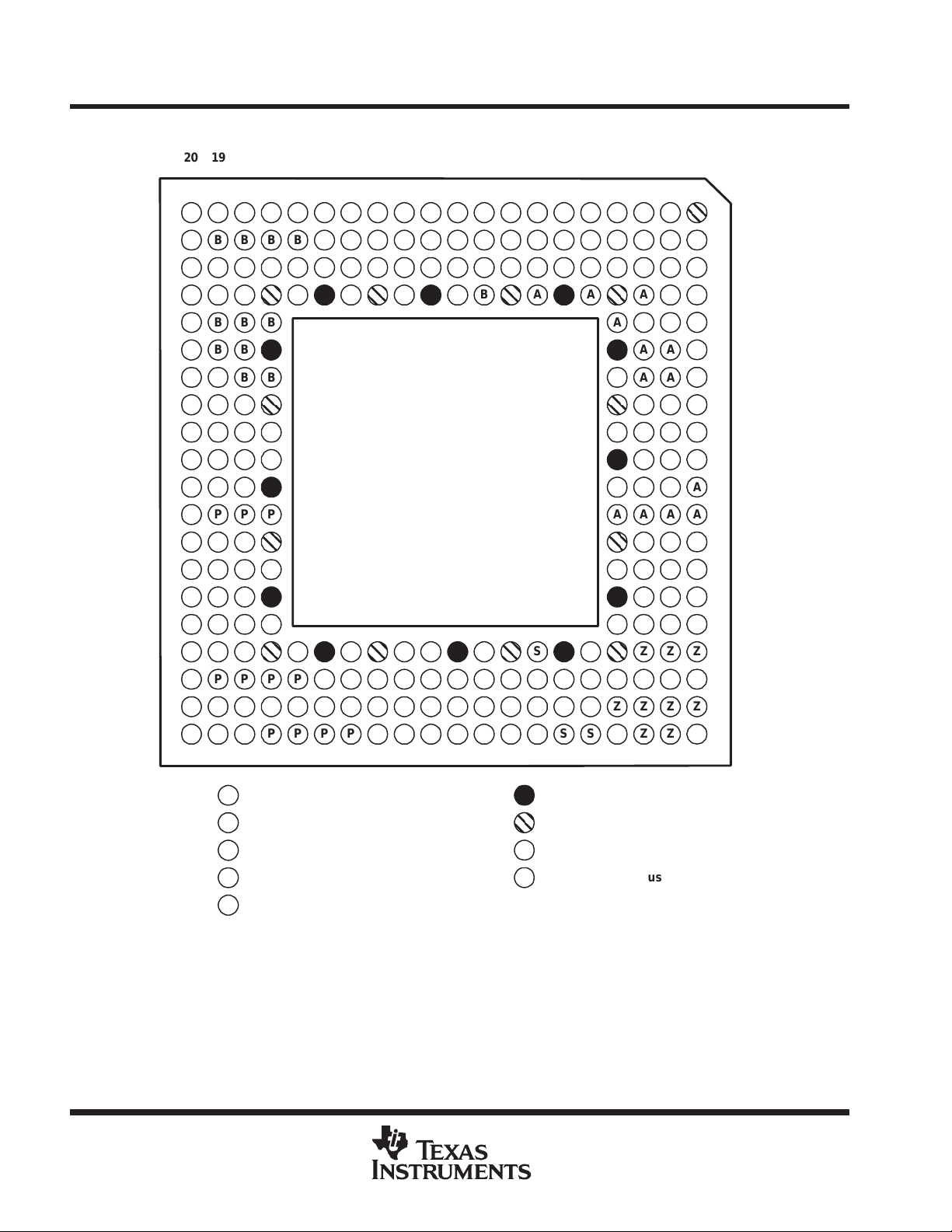
Figure 1. PCI4450 Pin Diagram
4
POST OFFICE BOX 655303 • DALLAS, TEXAS 75265
PCI4450 GFN/GJG
PC Card and OHCI Controller
SCPS046 – JANUAR Y 1999
signal names and terminal assignments
Signal names and their terminal assignments are shown in Tables 1 and 2 and are sorted alphanumerically by
the assigned terminal.
Table 1. GFN Terminals Sorted Alphanumerically for CardBus // 16-bit Signals and OHCI
GFN SIGNAL NAME GFN SIGNAL NAME GFN SIGNAL NAME
A1
A2
A3
A4
A5
A6
A7
A8
A9
A10
A11
A12
A13
A14
A15
A16
A17
A18
A19
A20
B1
B2
B3
B4
B5
B6
B7
B8
B9
B10
B11
B12
B13
B14
B15
B16
B17
B18
B19
B20
C1
C2
C3
C4
C5
C6
C7
C8
GND
A_CAD16//A_A17
A_CAD1 1//A_OE
A_CC/BE0//A_CE1
A_RSVD//A_D14
A_CAD3//A_D5
A_CAD1//A_D4
A_CCD1//A_CD1
B_CAD29//B_D1
B_CCLKRUN//B_WP(IOIS16)
B_CSTSCHG//B_BVD1(STSCHG/RI)
B_CINT//B_READY(IREQ)
B_CAD24//B_A2
B_CAD23//B_A3
B_CAD21//B_A5
B_CAD19//B_A25
B_CC/BE2//B_A12
B_CFRAME//B_A23
B_CGNT//B_WE
B_CSTOP//B_A20
A_RSVD//A_A18
A_CAD14//A_A9
A_CAD15//A_IOWR
A_CAD10//A_CE2
V
CCA
A_CAD5//A_D6
A_CAD4//A_D12
A_CAD0//A_D3
B_CAD30//B_D9
B_CCD2//B_CD2
B_CSERR//B_WAIT
B_CVS1//B_VS1
V
CCB
B_CREQ//B_INPACK
B_CRST//B_RESET
B_CAD18//B_A7
B_CCLK//B_A16
B_CDEVSEL//B_A21
B_CPERR//B_A14
B_CPAR//B_A13
A_CGNT//A_WE
A_CPAR//A_A13
A_CC/BE1//A_A8
A_CAD12//A_A11
A_CAD9//A_A10
A_CAD8//A_D15
A_CAD6//A_D13
A_CAD2//A_D11
C9
C10
C11
C12
C13
C14
C15
C16
C17
C18
C19
C20
D1
D2
D3
D4
D5
D6
D7
D8
D9
D10
D11
D12
D13
D14
D15
D16
D17
D18
D19
D20
E1
E2
E3
E4
E17
E18
E19
E20
F1
F2
F3
F4
F17
F18
F19
F20
B_RSVD//B_D2
B_CAD27//B_D0
B_CAUDIO//B_BVD2(SPKR)
B_CAD26//B_A0
B_CC/BE3//B_REG
B_CAD22//B_A4
B_CVS2//B_VS2
B_CAD17//B_A24
B_CTRDY//B_A22
B_CBLOCK//B_A19
B_RSVD//B_A18
B_CAD14//B_A9
A_CDEVSEL//A_A21
A_CBLOCK//A_A19
A_CPERR//A_A14
GND
A_CAD13//A_IORD
V
CC
A_CAD7//A_D7
GND
B_CAD31//B_D10
B_CAD28//B_D8
V
CC
B_CAD25//B_A1
GND
B_CAD20//B_A6
V
CC
B_CIRDY//B_A15
GND
B_CC/BE1//B_A8
B_CAD15//B_IOWR
B_CAD13//B_IORD
A_CIRDY//A_A15
A_CTRDY//A_A22
A_CCLK//A_A16
A_CSTOP//A_A20
B_CAD16//B_A17
B_CAD12//B_A11
V
CCB
B_CAD9//B_A10
A_CAD17//A_A24
A_CC/BE2//A_A12
V
CCA
V
CC
V
CC
B_CAD11//B_OE
B_CC/BE0//B_CE1
B_CAD7//B_D7
G1
A_CVS2//A_VS2
G2
A_CAD19//A_A25
G3
A_CAD18//A_A7
G4
A_CFRAME//A_A23
G17
B_CAD10//B_CE2
G18
B_CAD8//B_D15
G19
B_RSVD//B_D14
G20
B_CAD5//B_D6
H1
A_CAD21//A_A5
H2
A_CRST//A_RESET
H3
A_CAD20//A_A6
H4
GND
H17
GND
H18
B_CAD6//B_D13
H19
B_CAD3//B_D5
H20
B_CAD4//B_D12
J1
A_CC/BE3//A_REG
J2
A_CAD23//A_A3
J3
A_CREQ//A_INPACK
J4
A_CAD22//A_A4
J17
B_CAD1//B_D4
J18
B_CAD2//B_D11
J19
B_CAD0//B_D3
J20
B_CCD1//B_CD1
K1
A_CAD26//A_A0
K2
A_CAD24//A_A2
K3
A_CAD25//A_A1
K4
V
K17
K18
K19
K20
L1
L2
L3
L4
L17
L18
L19
L20
M1
M2
M3
M4
M17
M18
M19
M20
CC
PCLK
CLKRUN
PRST
GNT
A_CVS1//A_VS1
A_CINT//A_READY(IREQ)
A_CSERR//A_WAIT
V
CCA
V
CC
AD31
AD30
REQ
A_CAUDIO//A_BVD2(SPKR)
A_CSTSCHG//A_BVD1(STSCHG/RI)
A_CCLKRUN//A_WP(IOIS16)
A_CCD2//A_CD2
AD26
AD27
AD28
AD29
POST OFFICE BOX 655303 • DALLAS, TEXAS 75265
5
PCI4450 GFN/GJG
PC Card and OHCI Controller
SCPS046 – JANUAR Y 1999
signal names and terminal assignments (continued)
Table 1. GFN Terminals Sorted Alphanumerically for CardBus // 16-bit Signals and OHCI (Continued)
GFN SIGNAL NAME GFN SIGNAL NAME GFN SIGNAL NAME
N1
N2
N3
N4
N17
N18
N19
N20
P1
P2
P3
P4
P17
P18
P19
P20
R1
R2
R3
R4
R17
R18
R19
R20
T1
T2
T3
T4
T17
T18
T19
T20
U1
U2
U3
U4
U5
U6
A_CAD27//A_D0
A_CAD28//A_D8
A_CAD29//A_D1
GND
GND
C/BE3
AD24
AD25
A_CAD30//A_D9
A_RSVD//A_D2
ZV_HREF
ZV_Y1
AD20
AD23
V
CCP
IDSEL/MFUNC7
A_CAD31//A_D10
ZV_VSYNC
ZV_Y2
V
CC
V
CC
AD19
AD21
AD22
ZV_Y0
ZV_Y3
ZV_Y5
ZV_UV0
IRDY
AD16
AD17
AD18
ZV_Y4
ZV_Y6
ZV_UV2
GND
ZV_SDATA
V
CC
U7
U8
U9
U10
U11
U12
U13
U14
U15
U16
U17
U18
U19
U20
V1
V2
V3
V4
V5
V6
V7
V8
V9
V10
V11
V12
V13
V14
V15
V16
V17
V18
V19
V20
W1
W2
W3
PHY_CTL0
GND
PHY_DATA6
V
CC
SUSPEND
CLOCK
GND
AD6
V
CC
AD12
GND
TRDY
DEVSEL
C/BE2
ZV_Y7
ZV_UV1
ZV_UV3
ZV_LRCLK
MFUNC5
PHY_CLK
PHY_DATA0
PHY_DATA3
PHY_DATA7
MFUNC3
SPKROUT
DATA
AD0
V
CCP
AD7
AD9
AD13
C/BE1
STOP
FRAME
ZV_UV4
ZV_UV6
ZV_SCLK
W4
W5
W6
W7
W8
W9
W10
W11
W12
W13
W14
W15
W16
W17
W18
W19
W20
Y1
Y2
Y3
Y4
Y5
Y6
Y7
Y8
Y9
Y10
Y11
Y12
Y13
Y14
Y15
Y16
Y17
Y18
Y19
Y20
ZV_MCLK
LPS
PHY_CTL1
PHY_DATA1
PHY_DATA4
MFUNC4
SCL
MFUNC0
LATCH
IRQSER
AD2
AD4
C/BE0
AD10
AD14
PAR
PERR
ZV_UV5
ZV_UV7
ZV_PCLK
MFUNC6
PHY_LREQ
LINKON
PHY_DATA2
PHY_DATA5
SDA
MFUNC2
MFUNC1
G_RST
RI_OUT
AD1
AD3
AD5
AD8
AD11
AD15
SERR
6
POST OFFICE BOX 655303 • DALLAS, TEXAS 75265
PCI4450 GFN/GJG
PC Card and OHCI Controller
SCPS046 – JANUAR Y 1999
signal names and terminal assignments (continued)
Table 2. GJG Terminals Sorted Alphanumerically for CardBus // 16-bit Signals and OHCI
NO. SIGNAL NAME NO. SIGNAL NAME NO. SIGNAL NAME
A2
A3
A4
A5
A6
A7
A8
A9
A10
A11
A12
A13
A14
A15
A16
A17
A18
B1
B2
B3
B4
B5
B6
B7
B8
B9
B10
B11
B12
B13
B14
B15
B16
B17
B18
B19
C1
C2
C18
C19
D1
D2
D4
D5
D6
D7
D8
D9
D10
D11
A_CC/BE1//A_A8
GND
A_CAD12//A_A11
A_CAD10//A_CE2
A_CAD8//A_D15
A_CAD3//A_D5
A_CAD0//A_D3
B_CAD29//B_D1
B_CSTSCHG//B_BVD1(STSCHG /RI )
V
CC
B_CC/BE3//B_REG
B_CREQ//B_INPACK
B_CVS2//B_VS2
B_CAD17//B_A24
GND
B_CCLK//B_A16
B_CDEVSEL//B_A21
A_CPAR//A_A13
A_RSVD//A_A18
A_CAD16//A_A17
A_CAD15//A_IOWR
A_CAD11//A_OE
V
CCA
A_CAD6//A_D13
A_CAD2//A_D11
B_CAD30//B_D9
B_CCLKRUN//B_WP(IOIS16)
B_CVS1//B_VS1
V
CCB
B_CAD22//B_A4
B_CAD20//B_A6
B_CAD18//B_A7
B_CIRDY//B_A15
B_CTRDY//B_A22
B_CGNT//B_WE
B_CSTOP//B_A20
GND
A_CBLOCK//A_A19
B_CPERR//B_A14
B_CPAR//B_A13
A_CPERR//A_A14
A_CSTOP//A_A20
A_CAD14//A_A9
A_CAD13//A_IORD
A_CC/BE0//A_CE1
A_CAD5//A_D6
GND
B_RSVD//B_D2
B_CCD2//B_CD2
B_CAD26//B_A0
D12
D13
D14
D15
D16
D18
D19
E1
E2
E4
E5
E6
E7
E8
E9
E10
E11
E12
E13
E14
E15
E16
E18
E19
F1
F2
F4
F5
F6
F7
F8
F9
F10
F11
F12
F13
F14
F15
F16
F18
F19
G1
G2
G4
G5
G6
G7
G13
G14
G15
B_CAD24//B_A2
B_CAD23//B_A3
V
CC
B_CFRAME//B_A23
B_CBLOCK//B_A19
B_RSVD//B_A18
B_CC/BE1//B_A8
V
CC
A_CCLK//A_A16
A_CGNT//A_WE
A_CDEVSEL//A_A21
V
CC
A_RSVD//A_D14
A_CAD1//A_D4
B_CAD31//B_D10
B_CAD27//B_D0
B_CINT//B_READY(IREQ)
B_CAD25//B_A1
B_CAD21//B_A5
B_CAD19//B_A25
B_CC/BE2//B_A12
B_CAD16//B_A17
B_CAD14//B_A9
V
CC
V
CCA
A_CFRAME//A_A23
A_CIRDY//A_A15
A_CTRDY//A_A22
A_CAD9//A_A10
A_CAD7//A_D7
A_CCD1//A_CD1
B_CAD28//B_D8
B_CAUDIO//B_BVD2(SPKR)
B_CSERR//B_WAIT
GND
B_CRST//B_RESET
B_CAD15//B_IOWR
B_CAD12//B_A11
B_CAD13//B_IORD
V
CCB
B_CAD11//B_OE
GND
A_CAD18//A_A7
A_CAD19//A_A25
A_CAD17//A_A24
A_CC/BE2//A_A12
A_CAD4//A_D12
B_CAD7//B_D7
B_CAD10//B_CE2
B_CAD9//B_A10
G16
B_CC/BE0//B_CE1
G18
B_CAD8//B_D15
G19
GND
H1
A_CAD20//A_A6
H2
A_CRST//A_RESET
H4
A_CAD21//A_A5
H5
A_CAD22//A_A4
H6
A_CVS2//A_VS2
H14
B_CAD4//B_D12
H15
B_RSVD//B_D14
H16
B_CAD5//B_D6
H18
B_CAD6//B_D13
H19
B_CAD3//B_D5
J1
A_CAD23//A_A3
J2
A_CC/BE3//A_REG
J4
A_CREQ//A_INPACK
J5
A_CAD24//A_A2
J6
A_CAD25//A_A1
J14
V
J15
J16
J18
J19
K1
K2
K4
K5
K6
K14
K15
K18
K19
L1
L2
L4
L5
L6
L14
L15
L16
L18
L19
M1
M2
M4
M5
M6
M14
M15
M16
CC
B_CAD1//B_D4
B_CAD2//B_D11
B_CAD0//B_D3
B_CCD1//B_CD1
A_CVS1//A_VS1
A_CINT//A_READY(IREQ)
A_CSERR//A_WAIT
V
CCA
A_CAD26//A_A0
GNT
PCLK
CLKRUN
PRST
A_CSTSCHG//A_BVD1(STSCHG/RI)
A_CCLKRUN//A_WP(IOIS16)
A_CCD2//A_CD2
A_CAD27//A_D0
A_CAUDIO//A_BVD2(SPKR)
REQ
AD31
AD28
AD30
AD29
A_CAD29//A_D1
GND
A_CAD30//A_D9
A_RSVD//A_D2
A_CAD28//A_D8
C/BE3
AD27
AD26
POST OFFICE BOX 655303 • DALLAS, TEXAS 75265
7
PCI4450 GFN/GJG
PC Card and OHCI Controller
SCPS046 – JANUAR Y 1999
signal names and terminal assignments (continued)
Table 2. GJG Terminals Sorted Alphanumerically for CardBus // 16-bit Signals and OHCI (Continued)
NO. SIGNAL NAME NO. SIGNAL NAME NO. SIGNAL NAME
M18
M19
N1
N2
N4
N5
N6
N7
N13
N14
N15
N16
N18
N19
P1
P2
P4
P5
P6
P7
P8
P9
P10
P11
P12
P13
P14
P15
P16
P18
P19
R1
R2
R4
R5
AD25
AD24
ZV_HREF
ZV_VSYNC
ZV_Y0
ZV_Y1
ZV_Y2
A_CAD31//A_D10
AD3
AD22
AD23
GND
V
CCP
IDSEL/MFUNC7
V
CC
ZV_Y3
ZV_Y4
ZV_Y5
ZV_Y6
LINKON
PHY_DATA3
MFUNC2
MFUNC1
G_RST
IRQSER
AD6
AD9
V
CC
AD19
AD21
AD20
ZV_Y7
ZV_UV0
ZV_UV2
MFUNC6
R6
R7
R8
R9
R10
R11
R12
R13
R14
R15
R16
R18
R19
T1
T2
T4
T5
T6
T7
T8
T9
T10
T11
T12
T13
T14
T15
T16
T18
T19
U1
U2
U18
U19
V1
PHY_LREQ
PHY_DATA0
PHY_DATA7
MFUNC3
SUSPEND
RI_OUT
AD2
AD5
AD8
AD16
C/BE2
AD18
AD17
ZV_UV1
ZV_UV4
GND
V
CC
PHY_CLK
GND
PHY_DATA6
MFUNC4
SPKROUT
CLOCK
AD1
AD4
C/BE0
AD12
C/BE1
FRAME
IRDY
ZV_UV3
ZV_UV6
TRDY
DEVSEL
ZV_UV5
V2
V3
V4
V5
V6
V7
V8
V9
V10
V11
V12
V13
V14
V15
V16
V17
V18
V19
W2
W3
W4
W5
W6
W7
W8
W9
W10
W11
W12
W13
W14
W15
W16
W17
W18
ZV_SCLK
ZV_LRCLK
ZV_PCLK
LPS
PHY_CTL1
PHY_DATA1
PHY_DATA5
SCL
V
CC
DATA
AD0
V
CC
GND
AD11
AD14
PAR
PERR
STOP
ZV_UV7
ZV_MCLK
ZV_SDATA
MFUNC5
PHY_CTL0
PHY_DATA2
PHY_DATA4
SDA
MFUNC0
LATCH
GND
V
CCP
AD7
AD10
AD13
AD15
SERR
8
POST OFFICE BOX 655303 • DALLAS, TEXAS 75265
PCI4450 GFN/GJG
PC Card and OHCI Controller
SCPS046 – JANUAR Y 1999
PCI4450 System Block Diagram
Figure 2 shows a simplified system implementation example using the PCI4450. The PCI interface includes
all address/data and control signals for PCI protocol. Highlighted in this diagram is the functionality supported
by the PCI4450. The PCI4450 supports PC/PCI DMA, PCI Way DMA (distributed DMA), PME wake-up from
D3
through D0, 4 interrupt modes, an integrated zoomed video port, and 12 multifunction pins (8 MFUNC,
cold
and 4 GPIO pins) that can be programmed for a wide variety of functions.
PCI Bus
Activity LED’ s
Real Time
Clock
CLKRUN
South Bridge
14
OHCI-PHY
Interface
IRQSER
DMA
PME
Zoomed Video
19 Video
4 Audio
Interrupt Routing Options:
Embedded
Controller
VGA
Controller
Audio
Codec
1) Serial ISA/Serial PCI
2) Serial ISA/Parallel PCI
TPS2206
Power
Switch
44
PC Card
Socket A
PC Card
Socket B
†
The PC Card interface is 68 pins for CardBus and 16-bit PC Cards. In zoomed-video mode 23 pins are used for routing the zoomed video signals
to the VGA controller .
Clock
2
68
23 for ZV†
68
23 for ZV
PCI4450
ZV
Enable
23
PHY
1394 Ports
Figure 2. PCI4450 System Block Diagram
POST OFFICE BOX 655303 • DALLAS, TEXAS 75265
9

PCI4450 GFN/GJG
I/O
PC Card and OHCI Controller
SCPS046 – JANUAR Y 1999
terminal functions
This section describes the PCI4450 terminal functions. The terminals are grouped in tables by functionality such
as PCI system function, power supply function, etc., for quick reference. The terminal numbers are also listed
for convenient reference.
Table 3. Power Supply
TERMINAL
NAME GFN NO. GJG NO.
GND
V
V
CCA
V
CCB
V
CCP
A1, D4, D8, D13, D17, H4, H17,
N4, N17, U4, U8, U13, U17
D6, D11, D15, F4, F17, K4, L17,
CC
R4, R17, U6, U10, U15
B5, F3, L4 B6, F1, K5
B13, E19 B12, F18
P19, V14 N18, W13 Clamp voltage for PCI signaling (3.3 Vdc or 5 Vdc)
A3, A16, C1, D8, F12, G1, G19,
M2, N16, T4, T7, V14, W12
A11, D14, E1, E6, E19, J14, P1,
P15, T5, V10, V13
Table 4. PC Card Power Switch
TERMINAL
NAME GFN NO. GJG NO.
CLOCK U12 T11 I/O
DAT A V12 V1 1 O
LATCH W12 W1 1 O
I/O
TYPE
3-line power switch clock. Information on the DA T A line is sampled at the rising edge of
CLOCK. This terminal defaults as an input which means an external clock source must
be used. If the internal ring oscillator is used, then an external CLOCK source is not
required. The internal oscillator may be enabled by setting bit 27 of the system control
register (PCI offset 80h) to a 1b.
A 43 kW pulldown resistor should be tied to this terminal.
3-line power switch data. DAT A is used to serially communicate socket power-control
information to the power switch.
3-line power switch latch. LA TCH is asserted by the PCI4450 to indicate to the PC Card
power switch that the data on the DA TA line is valid.
FUNCTION
Device ground terminals
Power supply terminal for core logic (3.3 Vdc)
Clamp voltage for PC Card A interface. Indicates Card A
signaling environment.
Clamp voltage for PC Card B interface. Indicates Card B
signaling environment.
FUNCTION
10
POST OFFICE BOX 655303 • DALLAS, TEXAS 75265
terminal functions (continued)
I/O
PCI4450 GFN/GJG
PC Card and OHCI Controller
SCPS046 – JANUAR Y 1999
Table 5. PCI System
TERMINAL
NAME GFN NO. GJG NO.
CLKRUN
PCLK K17 K15 I
PRST K19 K19 I
G_RST Y12 P11 I
K18 K18 I/O
I/O
TYPE
FUNCTION
PCI clock run. CLKRUN is used by the central resource to request permission to stop the
PCI clock or to slow it down, and the PCI4450 responds accordingly. If CLKRUN is not
implemented, then this pin should be tied low. CLKRUN is enabled by default by bit 1
(KEEPCLK) in the system control register .
PCI bus clock. PCLK provides timing for all transactions on the PCI bus. All PCI signals are
sampled at the rising edge of PCLK.
PCI reset. When the PCI bus reset is asserted, PRST causes the PCI4450 to place all output
buffers in a high-impedance state and reset all internal registers. When PRST is asserted,
the device is completely nonfunctional. After PRST is deasserted, the PCI4450 is in its
default state. When the SUSPEND mode is enabled, the device is protected from the PRST
and the internal registers are preserved. All outputs are placed in a high-impedance state,
but the contents of the registers are preserved.
Global reset. When the global reset is asserted, the G_RST signal causes the PCI4450 to
place all output buffers in a high-impedance state and reset all internal registers. When
G_RST is asserted, the device is completely in its default state. For systems that require
wake-up from D3, G_RST will normally be asserted only during initial boot. PRST should be
asserted following initial boot so that PME context is retained when transitioning from D3 to
D0. For systems that do not require wake-up from D3, G_RST should be tied to PRST.
POST OFFICE BOX 655303 • DALLAS, TEXAS 75265
11
PCI4450 GFN/GJG
I/O
PC Card and OHCI Controller
SCPS046 – JANUAR Y 1999
terminal functions (continued)
Table 6. PCI Address and Data
TERMINAL
NAME GFN NO. GJG NO.
AD31
AD30
AD29
AD28
AD27
AD26
AD25
AD24
AD23
AD22
AD21
AD20
AD19
AD18
AD17
AD16
AD15
AD14
AD13
AD12
AD1 1
AD10
AD9
AD8
AD7
AD6
AD5
AD4
AD3
AD2
AD1
AD0
C/BE3
C/BE2
C/BE1
C/BE0
PAR W19 V17 I/O
L18
L19
M20
M19
M18
M17
N20
N19
P18
R20
R19
P17
R18
T20
T19
T18
Y19
W18
V17
U16
Y18
W17
V16
Y17
V15
U14
Y16
W15
Y15
W14
Y14
V13
N18
U20
V18
W16
L15
L18
L19
L16
M15
M16
M18
M19
N15
N14
P18
P19
P16
R18
R19
R15
W17
V16
W16
T15
V15
W15
P14
R14
W14
P13
R13
T13
N13
R12
T12
V12
M14
R16
T16
T14
TYPE
I/O
PCI address/data bus. These signals make up the multiplexed PCI address and data bus on the
I/O
primary interface. During the address phase of a primary bus PCI cycle, AD31–AD0 contain a 32-bit
address or other destination information. During the data phase, AD31–AD0 contain data.
PCI bus commands and byte enables. These signals are multiplexed on the same PCI terminals.
During the address phase of a primary bus PCI cycle, C/BE3–C/BE0 define the bus command.
During the data phase, this 4-bit bus is used as byte enables. The byte enables determine which
I/O
byte paths of the full 32-bit data bus carry meaningful data. C/BE0 applies to byte 0 (AD7–AD0),
C/BE1 applies to byte 1 (AD15–AD8), C/BE2 applies to byte 2 (AD23–AD16), and C/BE3 applies to
byte 3 (AD31–AD24).
PCI bus parity. In all PCI bus read and write cycles, the PCI4450 calculates even parity across the
AD31–AD0 and C/BE3–C/BE0 buses. As an initiator during PCI cycles, the PCI4450 outputs this
parity indicator with a one-PCLK delay. As a target during PCI cycles, the calculated parity is
compared to the initiator’s parity indicator . A compare error results in the assertion of a parity error
(PERR).
FUNCTION
12
POST OFFICE BOX 655303 • DALLAS, TEXAS 75265
terminal functions (continued)
I/O
PCI4450 GFN/GJG
PC Card and OHCI Controller
SCPS046 – JANUAR Y 1999
Table 7. PCI Interface Control
TERMINAL
NAME GFN NO. GJG NO.
DEVSEL U19 U19 I/O
FRAME V20 T18 I/O
GNT K20 K14 I
LOCK
(MFUNC7)
IDSEL/MFUNC7 P20 N19 I
IRDY T17 T19 I/O
PERR
REQ L20 L14 O
SERR Y20 W18 O
STOP V19 V19 I/O
TRDY U18 U18 I/O
P20 N19 I/O
W20 V18 I/O
TYPE
I/O
PCI device select. The PCI4450 asserts DEVSEL to claim a PCI cycle as the target device.
As a PCI initiator on the bus, the PCI4450 monitors DEVSEL until a target responds. If no
target responds before timeout occurs, then the PCI4450 terminates the cycle with an
initiator abort.
PCI cycle frame. FRAME is driven by the initiator of a bus cycle. FRAME is asserted to
indicate that a bus transaction is beginning, and data transfers continue while this signal
is asserted. When FRAME is deasserted, the PCI bus transaction is in the final data phase.
PCI bus grant. GNT is driven by the PCI bus arbiter to grant the PCI4450 access to the PCI
bus after the current data transaction has completed. GNT may or may not follow a PCI
bus request, depending on the PCI bus parking algorithm.
PCI bus lock. MFUNC7/LOCK can be configured as PCI LOCK and used to gain exclusive
access downstream. Since this functionality is not typically used, other functions may be
accessed through this terminal. MFUNC7/LOCK defaults to and can be configured
through the multifunction routing status register.
Initialization device select. IDSEL selects the PCI4450 during configuration space
accesses. IDSEL can be connected to one of the upper 24 PCI address lines on the PCI
bus. If the LATCH terminal (W12/W11) has an external pulldown resistor, then this
terminal is configurable as MFUNC7 and IDSEL defaults to the AD23 terminal.
PCI initiator ready. IRDY indicates the PCI bus initiator’s ability to complete the current data
phase of the transaction. A data phase is completed on a rising edge of PCLK where both
IRDY and TRDY are asserted. Until IRDY and TRDY are both sampled asserted, wait
states are inserted.
PCI parity error indicator. PERR is driven by a PCI device to indicate that calculated parity
does not match P AR when PERR is enabled through bit 6 of the command register .
PCI bus request. REQ is asserted by the PCI4450 to request access to the PCI bus as an
initiator .
PCI system error. SERR is an output that is pulsed from the PCI4450 when enabled through
the command register , indicating a system error has occurred. The PCI4450 need not be
the target of the PCI cycle to assert this signal. When SERR is enabled in the bridge control
register, this signal also pulses, indicating that an address parity error has occurred on a
CardBus interface.
PCI cycle stop signal. STOP is driven by a PCI target to request the initiator to stop the
current PCI bus transaction. STOP is used for target disconnects and is commonly
asserted by target devices that do not support burst data transfers.
PCI target ready. TRDY indicates the primary bus target’s ability to complete the current
data phase of the transaction. A data phase is completed on a rising edge of PCLK when
both IRDY and TRDY are asserted. Until both IRDY and TRDY are asserted, wait states
are inserted.
FUNCTION
POST OFFICE BOX 655303 • DALLAS, TEXAS 75265
13
PCI4450 GFN/GJG
I/O
I/O
PC Card and OHCI Controller
SCPS046 – JANUAR Y 1999
terminal functions (continued)
Table 8. System Interrupt
TERMINAL
NAME GFN NO. GJG NO.
INTA
(MFUNC0)
INTB
(MFUNC1)
INTC
(MFUNC2)
IRQSER W13 P12 I/O
MFUNC6
MFUNC5
MFUNC4
MFUNC3
MFUNC2
MFUNC1
MFUNC0
RI_OUT/PME Y13 R11 O
W1 1 W10 I/O
Y11 P10 I/O
Y10 P9 I/O
Y4
V5
W9
V10
Y10
Y11
W1 1
R5
W5
T9
R9
P9
P10
W10
I/O
TYPE
FUNCTION
Parallel PCI interrupt. INTA can be mapped to MFUNC0 when parallel PCI interrupts are
used.
See
programmable interrupt subsystem
defaults to a general-purpose input.
Parallel PCI interrupt. INTB can be mapped to MFUNC1 when parallel PCI interrupts are
used.
See
programmable interrupt subsystem
defaults to a general-purpose input.
Parallel PCI interrupt. INTC can be mapped to MFUNC2 when parallel PCI interrupts are
used.
See
programmable interrupt subsystem
defaults to a general-purpose input.
Serial interrupt signal. IRQSER provides the IRQSER-style serial interrupting scheme.
Serialized PCI interrupts can also be sent in the IRQSER stream. See
interrupt subsystem
Interrupt request/secondary functions multiplexed. The primary function of these terminals
is to provide programmable options supported by the PCI4450. These interrupt multiplexer
outputs can be mapped to various functions. See
options.
All of these terminals have secondary functions, such as PCI interrupts, PC/PCI DMA, OHCI
O
LEDs, GPE request/grant, ring indicate output, and zoomed video status, that can be
selected with the appropriate programming of this register . When the secondary functions
are enabled, the respective terminals are not available for multifunction routing.
See the
multifunction routing status register
Ring indicate out and power management event output. T erminal provides an output to the
system for ring-indicate or PME signals. Alternately, RI_OUT can be routed on MFUNC7.
for details on interrupt signaling.
for details on interrupt signaling. MFUNC0/INTA
for details on interrupt signaling. MFUNC1/INTB
for details on interrupt signaling. MFUNC2/INTC
multifunction routing status register
for programming options.
programmable
for
TERMINAL
NAME GFN NO. GJG NO.
PCGNT
(MFUNC2)
PCGNT
(MFUNC3)
PCREQ
(MFUNC7)
PCREQ
(MFUNC4)
PCREQ
(MFUNC0)
Y10
V10
P20
W9
W1 1
N19
W10
P9
R9
T9
I/O
TYPE
I/O
O
Table 9. PC/PCI DMA
FUNCTION
PC/PCI DMA grant. PCGNT is used to grant the DMA channel to a requester in a system
supporting the PC/PCI DMA scheme. PCGNT, is available on MFUNC2 or MFUNC3.
This terminal is also used for the serial EEPROM interface.
PC/PCI DMA request. PCREQ is used to request DMA transfers as DREQ in a system
supporting the PC/PCI DMA scheme. PCREQ is available on MFUNC7, MFUNC4, or
MFUNC0.
This terminal is also used for the serial EEPROM interface.
14
POST OFFICE BOX 655303 • DALLAS, TEXAS 75265
terminal functions (continued)
I/O AND MEMORY
PCI4450 GFN/GJG
PC Card and OHCI Controller
SCPS046 – JANUAR Y 1999
Table 10. Zoomed Video
TERMINAL
NAME
ZV_HREF P3 N1 A10 O Horizontal sync to the zoomed video port
ZV_VSYNC R2 N2 A1 1 O Vertical sync to the zoomed video port
ZV_Y7
ZV_Y6
ZV_Y5
ZV_Y4
ZV_Y3
ZV_Y2
ZV_Y1
ZV_Y0
ZV_UV7
ZV_UV6
ZV_UV5
ZV_UV4
ZV_UV3
ZV_UV2
ZV_UV1
ZV_UV0
ZV_SCLK W3 V2 A7 O Audio SCLK PCM
ZV_MCLK W4 W3 A6 O Audio MCLK PCM
ZV_PCLK Y3 V4 IOIS16 O Pixel clock to the zoomed video port
ZV_LRCLK V4 V3 INP ACK O Audio LRCLK PCM
ZV_SDA T A U5 W4 SPKR O Audio SDATA PCM
GFN
NO.
V1
U2
T3
U1
T2
R3
P4
T1
Y2
W2
Y1
W1
V3
U3
V2
T4
GJG NO.
R1
P6
P5
P4
P2
N6
N5
N4
W2
U2
V1
T2
U1
R4
T1
R2
I/O AND MEMORY
INTERFACE
SIGNAL
A20
A14
A19
A13
A18
A8
A17
A9
A25
A12
A24
A15
A23
A16
A22
A21
I/O
TYPE
O Video data to the zoomed video port in YV:4:2:2 format
O Video data to the zoomed video port in YV:4:2:2 format
FUNCTION
POST OFFICE BOX 655303 • DALLAS, TEXAS 75265
15

PCI4450 GFN/GJG
PC Card and OHCI Controller
SCPS046 – JANUAR Y 1999
terminal functions (continued)
Table 11. Miscellaneous
TERMINAL
NAME
MFUNC0 W11 W10 I/O
MFUNC1 Y11 P10 I/O
MFUNC2
MFUNC3
MFUNC4
MFUNC5
MFUNC6 Y4 R5 I/O
IDSEL/MFUNC7 P20 N19 I/O
SCL W10 V9 I/O
SDA Y9 W9 I/O
SPKROUT
SUSPEND
GFN
NO.
Y10 P9 I/O
V10 R9 I/O
W9 T9 I/O
V5 W5 I/O
V11 T10 O
U11 R10 I
GJG
NO.
I/O
TYPE
FUNCTION
Multifunction terminal 0. Defaults as a general-purpose input (GPI0), and can be programmed
to perform various functions. Refer to
Multifunction terminal 1. Defaults as a general-purpose input (GPI1), and can be programmed
to perform various functions. Refer to
Multifunction terminal 2. Defaults as a general-purpose input (GPI2), and can be programmed
to perform various functions. Refer to
Multifunction terminal 3. Defaults as a general-purpose input (GPI3), and can be programmed
to perform various functions. Refer to
Multifunction terminal 4. Defaults as a high–impedance reserved input, and can be
programmed to perform various functions. Refer to
Multifunction terminal 5. Defaults as a high–impedance reserved input, and can be
programmed to perform various functions. Refer to
Multifunction terminal 6. Defaults as a high–impedance reserved input, and can be
programmed to perform various functions. Refer to
IDSEL and multifunction terminal 7. Defaults as IDSEL, but may be used as a multifunction
terminal. Refer to
Serial ROM clock. This terminal provides the SCL serial clock signaling in a two–wire serial
ROM implementation, and is sensed at reset for serial ROM detection.
Serial ROM data. This terminal provides the SDA serial data signaling in a two–wire serial ROM
implementation.
Speaker output. SPKROUT is the output to the host system that can carry SPKR or CAUDIO
through the PCI4450 from the PC Card interface. SPKROUT is driven as the XOR combination
of card SPKR//CAUDIO inputs.
Suspend. SUSPEND is used to protect the internal registers from clearing when PRST is
asserted. See
multifunction routing register
suspend mode
multifunction routing register
multifunction routing register
multifunction routing register
multifunction routing register
description and Section 3.4 for details.
for details.
description.
description.
description.
description.
multifunction routing register
multifunction routing register
multifunction routing register
description.
description.
description.
16
POST OFFICE BOX 655303 • DALLAS, TEXAS 75265

terminal functions (continued)
I/O
FUNCTION
Table 12. 16-bit PC Card Address and Data (slots A and B)
TERMINAL
GFN NO. GJG NO.
NAME
†
T erminal name for slot A is preceded with A_. For example, the full name for terminal G2 is A_A25.
‡
T erminal name for slot B is preceded with B_. For example, the full name for terminal A16 is B_A25.
A25
A24
A23
A22
A21
A20
A19
A18
A17
A16
A15
A14
A13
A12
A11
A10
A9
A8
A7
A6
A5
A4
A3
A2
A1
A0
D15
D14
D13
D12
D11
D10
D9
D8
D7
D6
D5
D4
D3
D2
D1
D0
SLOT
†
A
G2
F1
G4
E2
D1
E4
D2
B1
A2
E3
E1
D3
C2
F2
C4
C5
B2
C3
G3
H3
H1
J4
J2
K2
K3
K1
C6
A5
C7
B7
C8
R1
P1
N2
D7
B6
A6
A7
B8
P2
N3
N1
SLOT
‡
B
A16
C16
A18
C17
B18
A20
C18
C19
E17
B17
D16
B19
B20
A17
E18
E20
C20
D18
B16
D14
A15
C14
A14
A13
D12
C12
G18
G19
H18
H20
J18
D9
B9
D10
F20
G20
H19
J17
J19
C9
A9
C10
SLOT
†
A
G4
G5
F2
F5
E5
D2
C2
B2
B3
E2
F4
D1
B1
G6
A4
F6
D4
A2
G2
H1
H4
H5
J1
J5
J6
K6
A6
E7
B7
G7
B8
N7
M4
M6
F7
D7
A7
E8
A8
M5
M1
L5
SLOT
B
E14
A15
D15
B17
A18
B19
D16
D18
E16
A17
B16
C18
C19
E15
F15
G15
E18
D19
B15
B14
E13
B13
D13
D12
E12
D11
G18
H15
H18
H14
J16
E9
B9
F9
G13
H16
H19
J15
J18
D9
A9
E10
I/O
TYPE
‡
O PC Card address. 16-bit PC Card address lines. A25 is the most significant bit.
I/O PC Card data. 16-bit PC Card data lines. D15 is the most significant bit.
PCI4450 GFN/GJG
PC Card and OHCI Controller
SCPS046 – JANUAR Y 1999
POST OFFICE BOX 655303 • DALLAS, TEXAS 75265
17
PCI4450 GFN/GJG
I/O
FUNCTION
PC Card and OHCI Controller
SCPS046 – JANUAR Y 1999
terminal functions (continued)
Table 13. 16-bit PC Card Interface Control (slots A and B)
TERMINAL
GFN NO. GJG NO.
NAME
BVD1
(STSCHG/RI)
BVD2
(SPKR)
CD1
CD2
CE1
CE2
INPACK J3 B14 J4 A13 I
IORD D5 D20 D5 F16 O
IOWR B3 D19 B4 F14 O
SLOT
SLOT
SLOT
†
A
M2 A11 L1 A10 I
M1 C11 L6 F10 I
A8M4J20
A4B4F19
‡
B
B10F8L4
G17D6A5
SLOT
†
A
B
J19
D10
G16
G14
I/O
TYPE
‡
Battery voltage detect 1. BVD1 is generated by 16-bit memory PC Cards that
include batteries. BVD1 and BVD2 indicate the condition of the batteries on a
memory PC Card. Both BVD1 and BVD2 are kept high when the battery is good.
When BVD2 is low and BVD1 is high, the battery is weak and should be replaced.
When BVD1 is low, the battery is no longer serviceable and the data in the memory
PC Card is lost. See ExCA card status-change interrupt configuration register for
the enable bits. See ExCA card status-change register and the ExCA interface
status register for the status bits for this signal.
Status change. STSCHG is used to alert the system to a change in the READY ,
write protect, or battery voltage dead condition of a 16-bit I/O PC Card.
Ring indicate. RI is used by 16-bit modem cards to indicate a ring detection.
Battery voltage detect 2. BVD2 is generated by 16-bit memory PC Cards that
include batteries. BVD2 and BVD1 indicate the condition of the batteries on a
memory PC Card. Both BVD1 and BVD2 are high when the battery is good. When
BVD2 is low and BVD1 is high, the battery is weak and should be replaced. When
BVD1 is low, the battery is no longer serviceable and the data in the memory PC
Card is lost. See ExCA card status-change interrupt configuration register for
enable bits. See ExCA card status-change register and the ExCA interface status
register for the status bits for this signal.
Speaker . SPKR is an optional binary audio signal available only when the card and
socket have been configured for the 16-bit I/O interface. The audio signals from
cards A and B are combined by the PCI4450 and are output on SPKROUT.
DMA request. BVD2 can be used as the DMA request signal during DMA
operations to a 16-bit PC Card that supports DMA. The PC Card asserts BVD2 to
indicate a request for a DMA operation.
PC Card detect 1 and PC Card detect 2. CD1 and CD2 are internally connected
I
to ground on the PC Card. When a PC Card is inserted into a socket, CD1 and CD2
are pulled low. For signal status, see ExCA interface status register.
Card enable 1 and card enable 2. CE1 and CE2 enable even- and odd-numbered
O
address bytes. CE1 enables even-numbered address bytes, and CE2 enables
odd-numbered address bytes.
Input acknowledge. INP ACK is asserted by the PC Card when it can respond to an
I/O read cycle at the current address.
DMA request. INPACK can be used as the DMA request signal during DMA
operations from a 16-bit PC Card that supports DMA. If used as a strobe, the PC
Card asserts this signal to indicate a request for a DMA operation.
I/O read. IORD is asserted by the PCI4450 to enable 16-bit I/O PC Card data output
during host I/O read cycles.
DMA write. IORD is used as the DMA write strobe during DMA operations from a
16-bit PC Card that supports DMA. The PCI4450 asserts IORD during DMA
transfers from the PC Card to host memory .
I/O write. IOWR is driven low by the PCI4450 to strobe write data into 16-bit I/O PC
Cards during host I/O write cycles.
DMA read. IOWR is used as the DMA write strobe during DMA operations from a
16-bit PC Card that supports DMA. The PCI4450 asserts IOWR during transfers
from host memory to the PC Card.
18
POST OFFICE BOX 655303 • DALLAS, TEXAS 75265
PC Card and OHCI Controller
I/O
FUNCTION
terminal functions (continued)
Table 13. 16-bit PC Card Interface Control (slots A and B) (continued)
TERMINAL
GFN NO. GJG NO.
NAME
OE A3 F18 B5 F19 O
READY
(IREQ)
REG J1 C13 J2 A12 O
RESET H2 B15 H2 F13 O PC Card reset. RESET forces a hard reset to a 16-bit PC Card.
WAIT
WE C1 A19 E4 B18 O
WP
(IOIS16)
VS1
VS2
†
T erminal name for slot A is preceded with A_. For example, the full name for terminal C1 is A_WE.
‡
T erminal name for slot B is preceded with B_. For example, the full name for terminal A19 is B_WE.
SLOT
SLOT
†
A
L2 A12 K2 E11 I
L3 B1 1 K4 F11 I
M3 A10 L2 B10 I
L1G1B12
SLOT
‡
B
C15K1H6
SLOT
†
A
B11
A14
I/O
TYPE
‡
B
Output enable. OE is driven low by the PCI4450 to enable 16-bit memory PC Card
data output during host memory read cycles.
DMA terminal count. OE is used as terminal count (TC) during DMA operations to
a 16-bit PC Card that supports DMA. The PCI4450 asserts OE to indicate TC for
a DMA write operation.
Ready . The ready function is provided by READY when the 16-bit PC Card and the
host socket are configured for the memory-only interface. READY is driven low by
the 16-bit memory PC Cards to indicate that the memory card circuits are busy
processing a previous write command. READY is driven high when the 16-bit
memory PC Card is ready to accept a new data transfer command.
Interrupt request. IREQ is asserted by a 16-bit I/O PC Card to indicate to the host
that a device on the 16-bit I /O PC Card requires service by the host software.
IREQ is high (deasserted) when no interrupt is requested.
Attribute memory select. REG remains high for all common memory accesses.
When REG is asserted, access is limited to attribute memory (OE or WE active)
and to the I/O space (IORD or IOWR active). Attribute memory is a separately
accessed section of card memory and is generally used to record card capacity
and other configuration and attribute information.
DMA acknowledge. REG is used as a DMA acknowledge (DACK) during DMA
operations to a 16-bit PC Card that supports DMA. The PCI4450 asserts REG to
indicate a DMA operation. REG is used in conjunction with the DMA read (IOWR)
or DMA write (IORD) strobes to transfer data.
Bus cycle wait. WAIT is driven by a 16-bit PC Card to delay the completion of (i.e.,
extend) the memory or I/O cycle in progress.
Write enable. WE is used to strobe memory write data into 16-bit memory PC
Cards. WE is also used for memory PC Cards that employ programmable memory
technologies.
DMA terminal count. WE is used as TC during DMA operations to a 16-bit PC Card
that supports DMA. The PCI4450 asserts WE to indicate TC for a DMA read
operation.
Write protect. WP applies to 16-bit memory PC Cards. WP reflects the status of the
write-protect switch on 16-bit memory PC Cards. For 16-bit I/O cards, WP is used
for the 16-bit port (IOIS16) function.
I/O is 16 bits. IOIS16 applies to 16-bit I/O PC Cards. IOIS16 is asserted by the 16-bit
PC Card when the address on the bus corresponds to an address to which the
16-bit PC Card responds, and the I/O port that is addressed is capable of 16-bit
accesses.
DMA request. WP can be used as the DMA request signal during DMA operations
to a 16-bit PC Card that supports DMA. If used, the PC Card asserts WP to indicate
a request for a DMA operation.
Voltage sense 1 and voltage sense 2. VS1 and VS2, when used in conjunction
I/O
with each other, determine the operating voltage of the 16-bit PC Card.
PCI4450 GFN/GJG
SCPS046 – JANUAR Y 1999
POST OFFICE BOX 655303 • DALLAS, TEXAS 75265
19
PCI4450 GFN/GJG
I/O
FUNCTION
PC Card and OHCI Controller
SCPS046 – JANUAR Y 1999
terminal functions (continued)
Table 14. CardBus PC Card Interface System (slots A and B)
TERMINAL
GFN NO. GJG NO.
NAME
CCLK E3 B17 E2 A17 O
CCLKRUN
CRST H2 B15 H2 F13 I/O
†
T erminal name for slot A is preceded with A_. For example, the full name for terminal E3 is A_CCLK.
‡
T erminal name for slot B is preceded with B_. For example, the full name for terminal B17 is B_CCLK.
SLOT
SLOT
SLOT
†
A
M3 A10 L2 B10 O
‡
B
SLOT
†
A
I/O
TYPE
‡
B
CardBus PC Card clock. CCLK provides synchronous timing for all transactions on
the CardBus interface. All signals except CRST, CCLKRUN, CINT, CSTSCHG,
CAUDIO, CCD2, CCD1, and CVS2–CVS1 are sampled on the rising edge of CCLK,
and all timing parameters are defined with the rising edge of this signal. CCLK
operates at the PCI bus clock frequency, but it can be stopped in the low state or
slowed down for power savings.
CardBus PC Card clock run. CCLKRUN is used by a CardBus PC Card to request
an increase in the CCLK frequency , and by the PCI4450 to indicate that the CCLK
frequency is decreased. CardBus clock run (CCLKRUN) follows the PCI clock run
(CLKRUN).
CardBus PC Card reset. CRST is used to bring CardBus PC Card-specific registers,
sequencers, and signals to a known state. When CRST is asserted, all CardBus PC
Card signals must be placed in a high-impedance state, and the PCI4450 drives
these signals to a valid logic level. Assertion can be asynchronous to CCLK, but
deassertion must be synchronous to CCLK.
20
POST OFFICE BOX 655303 • DALLAS, TEXAS 75265
terminal functions (continued)
I/O
FUNCTION
Table 15. CardBus PC Card Address and Data (slots A and B)
TERMINAL
GFN NO. GJG NO.
NAME
CAD31
CAD30
CAD29
CAD28
CAD27
CAD26
CAD25
CAD24
CAD23
CAD22
CAD21
CAD20
CAD19
CAD18
CAD17
CAD16
CAD15
CAD14
CAD13
CAD12
CAD11
CAD10
CAD9
CAD8
CAD7
CAD6
CAD5
CAD4
CAD3
CAD2
CAD1
CAD0
CC/BE3
CC/BE2
CC/BE1
CC/BE0
CPAR C2 B20 B1 C19 I/O
†
T erminal name for slot A is preceded with A_. For example, the full name for terminal C2 is A_CP AR.
‡
T erminal name for slot B is preceded with B_. For example, the full name for terminal B20 is B_CP AR.
SLOT
†
A
R1
P1
N3
N2
N1
K1
K3
K2
J2
J4
H1
H3
G2
G3
F1
A2
B3
B2
D5
C4
A3
B4
C5
C6
D7
C7
B6
B7
A6
C8
A7
B8
J1
F2
C3
A4
SLOT
‡
B
D9
B9
A9
D10
C10
C12
D12
A13
A14
C14
A15
D14
A16
B16
C16
E17
D19
C20
D20
E18
F18
G17
E20
G18
F20
H18
G20
H20
H19
J18
J17
J19
C13
A17
D18
F19
SLOT
†
A
N7
M4
M1
M6
L5
K6
J6
J5
J1
H5
H4
H1
G4
G2
G5
B3
B4
D4
D5
A4
B5
A5
F6
A6
F7
B7
D7
G7
A7
B8
E8
A8
J2
G6
A2
D6
SLOT
E10
D11
E12
D12
D13
B13
E13
B14
E14
B15
A15
E16
F14
E18
F16
F15
F19
G14
G15
G18
G13
H18
H16
H14
H19
J16
J15
J18
A12
E15
D19
G16
B
E9
B9
A9
F9
I/O
TYPE
‡
PC Card address and data. These signals make up the multiplexed CardBus address
and data bus on the CardBus interface. During the address phase of a CardBus cycle,
I/O
CAD31–CAD0 contain a 32-bit address. During the data phase of a CardBus cycle,
CAD31–CAD0 contain data. CAD31 is the most significant bit.
CardBus bus commands and byte enables. CC/BE3–CC/BE0 are multiplexed on the
same CardBus terminals. During the address phase of a CardBus cycle,
CC/BE3–CC/BE0 defines the bus command. During the data phase, this 4-bit bus is
used as byte enables. The byte enables determine which byte paths of the full 32-bit
I/O
data bus carry meaningful data. CC/BE0 applies to byte 0 (CAD7–CAD0), CC/BE1
applies to byte 1 (CAD15–CAD8), CC/BE2 applies to byte 2 (CAD23–CAD16), and
CC/BE3 applies to byte 3 (CAD31–CAD24).
CardBus parity . In all CardBus read and write cycles, the PCI4450 calculates even parity
across the CAD and CC/BE buses. As an initiator during CardBus cycles, the PCI4450
outputs CP AR with a one-CCLK delay . As a target during CardBus cycles, the calculated
parity is compared to the initiator’s parity indicator; a compare error results in a parity
error assertion.
PCI4450 GFN/GJG
PC Card and OHCI Controller
SCPS046 – JANUAR Y 1999
POST OFFICE BOX 655303 • DALLAS, TEXAS 75265
21
PCI4450 GFN/GJG
I/O
FUNCTION
CCD1
A8M4J20
J19
PC Card and OHCI Controller
SCPS046 – JANUAR Y 1999
terminal functions (continued)
Table 16. CardBus PC Card Interface Control (slots A and B)
TERMINAL
GFN NO. GJG NO.
NAME
CAUDIO M1 C11 L6 F10 I
CBLOCK D2 C18 C2 D16 I/O CardBus lock. CBLOCK is used to gain exclusive access to a target.
CCD1
CCD2
CDEVSEL D1 B18 E5 A18 I/O
CFRAME G4 A18 F2 D15 I/O
CGNT
CINT
CIRDY E1 D16 F4 B16 I/O
CPERR D3 B19 D1 C18 I/O
CREQ
CSERR L3 B11 K4 F1 1 I
CSTOP E4 A20 D2 B19 I/O
CSTSCHG
CTRDY E2 C17 F5 B17 I/O
CVS1
CVS2
†
T erminal name for slot A is preceded with A_. For example, the full name for terminal M1 is A_CAUDIO.
‡
T erminal name for slot B is preceded with B_. For example, the full name for terminal C1 1 is B_CAUDIO.
SLOT
SLOT
SLOT
†
A
A8 J20 F8 J19
C1 A19 E4 B18 I
L2 A12 K2 E1 1 I
J3 B14 J4 A13 I
M2 A11 L1 A10 I
L1G1B12
‡
B
B10F8L4
C15K1H6
SLOT
†
A
D10
B11
A14
I/O
TYPE
‡
B
CardBus audio. CAUDIO is a digital input signal from a PC Card to the system
speaker . The PCI4450 supports the binary audio mode and outputs a binary signal
from the card to SPKROUT .
CardBus detect 1 and CardBus detect 2. CCD1 and CCD2 are used in conjunction
I with CVS1 and CVS2 to identify card insertion and interrogate cards to determine the
operating voltage and card type.
CardBus device select. The PCI4450 asserts CDEVSEL to claim a CardBus cycle
as the target device. As a CardBus initiator on the bus, the PCI4450 monitors
CDEVSEL until a target responds. If no target responds before timeout occurs, then
the PCI4450 terminates the cycle with an initiator abort.
CardBus cycle frame. CFRAME is driven by the initiator of a CardBus bus cycle.
CFRAME is asserted to indicate that a bus transaction is beginning, and data
transfers continue while this signal is asserted. When CFRAME is deasserted, the
CardBus bus transaction is in the final data phase.
CardBus bus grant. CGNT is driven by the PCI4450 to grant a CardBus PC Card
access to the CardBus bus after the current data transaction has been completed.
CardBus interrupt. CINT is asserted low by a CardBus PC Card to request interrupt
servicing from the host.
CardBus initiator ready. CIRDY indicates the CardBus initiator’s ability to complete
the current data phase of the transaction. A data phase is completed on a rising edge
of CCLK when both CIRDY and CTRDY are asserted. Until CIRDY and CTRDY are
both sampled asserted, wait states are inserted.
CardBus parity error. CPERR is used to report parity errors during CardBus
transactions, except during special cycles. It is driven low by a target two clocks
following that data when a parity error is detected.
CardBus request. CREQ indicates to the arbiter that the CardBus PC Card desires
use of the CardBus bus as an initiator.
CardBus system error . CSERR reports address parity errors and other system errors
that could lead to catastrophic results. CSERR is driven by the card synchronous to
CCLK, but deasserted by a weak pullup, and may take several CCLK periods. The
PCI4450 can report CSERR to the system by assertion of SERR on the PCI interface.
CardBus stop. CSTOP is driven by a CardBus target to request the initiator to stop
the current CardBus transaction. CSTOP is used for target disconnects, and is
commonly asserted by target devices that do not support burst data transfers.
CardBus status change. CSTSCHG is used to alert the system to a change in the
card’s status and is used as a wake-up mechanism.
CardBus target ready . CTRDY indicates the CardBus target’s ability to complete the
current data phase of the transaction. A data phase is completed on a rising edge of
CCLK, when both CIRDY and CTRDY are asserted; until this time, wait states are
inserted.
CardBus voltage sense 1 and CardBus voltage sense 2. CVS1 and CVS2 are used
I/O
in conjunction with CCD1 and CCD2 to identify card insertion and interrogate cards
to determine the operating voltage and card type.
22
POST OFFICE BOX 655303 • DALLAS, TEXAS 75265
terminal functions (continued)
I/O
System cloc
des a 49.15
a
System clock. This in ut rovides a 49.152 MHz clock signal for data
Table 17. IEEE1394 PHY/Link Interface Terminals
PCI4450 GFN/GJG
PC Card and OHCI Controller
SCPS046 – JANUAR Y 1999
TERMINAL
NAME GFN NO. GJG NO.
PHY_CTL1
PHY_CTL0
PHY_DA T A7
PHY_DA T A6
PHY_DA T A5
PHY_DA T A4
PHY_DA T A3
PHY_DA T A2
PHY_DA T A1
PHY_DA T A0
PHY_CLK V6 T6 I
PHY_LREQ Y5 R6 O
LINKON Y6 P7 I 1394 link on. This input from the PHY indicates that the link should turn on.
LPS W5 V5 O Link power status. LPS indicates that link is powered and fully functional.
W6
U7
V9
U9
Y8
W8
V8
Y7
W7
V7
V6
W6
R8
T8
V8
W8
P8
W7
V7
R7
I/O
TYPE
I/O
I/O
FUNCTION
Phy–link interface control. These bi-direction signals control passage of
information between the PHY and link. The link can only drive these terminals
after the PHY has granted permission following a link request (LREQ).
Phy–link interface data. These bi-directional signals pass data between the PHY
and link. These terminals are driven by the link on transmissions and are driven
by the PHY on receptions. Only DATA1–DATA0 are valid for 100 Mbit speed.
DATA4–DATA0 are valid for 200 Mbit speed and DATA7–DATA0 are valid for
400 Mbit speed.
k. This input provi
synchronization.
Link request. This signal is driven by the link to initiate a request for the PHY to
perform some service.
2 MHz clock signal for dat
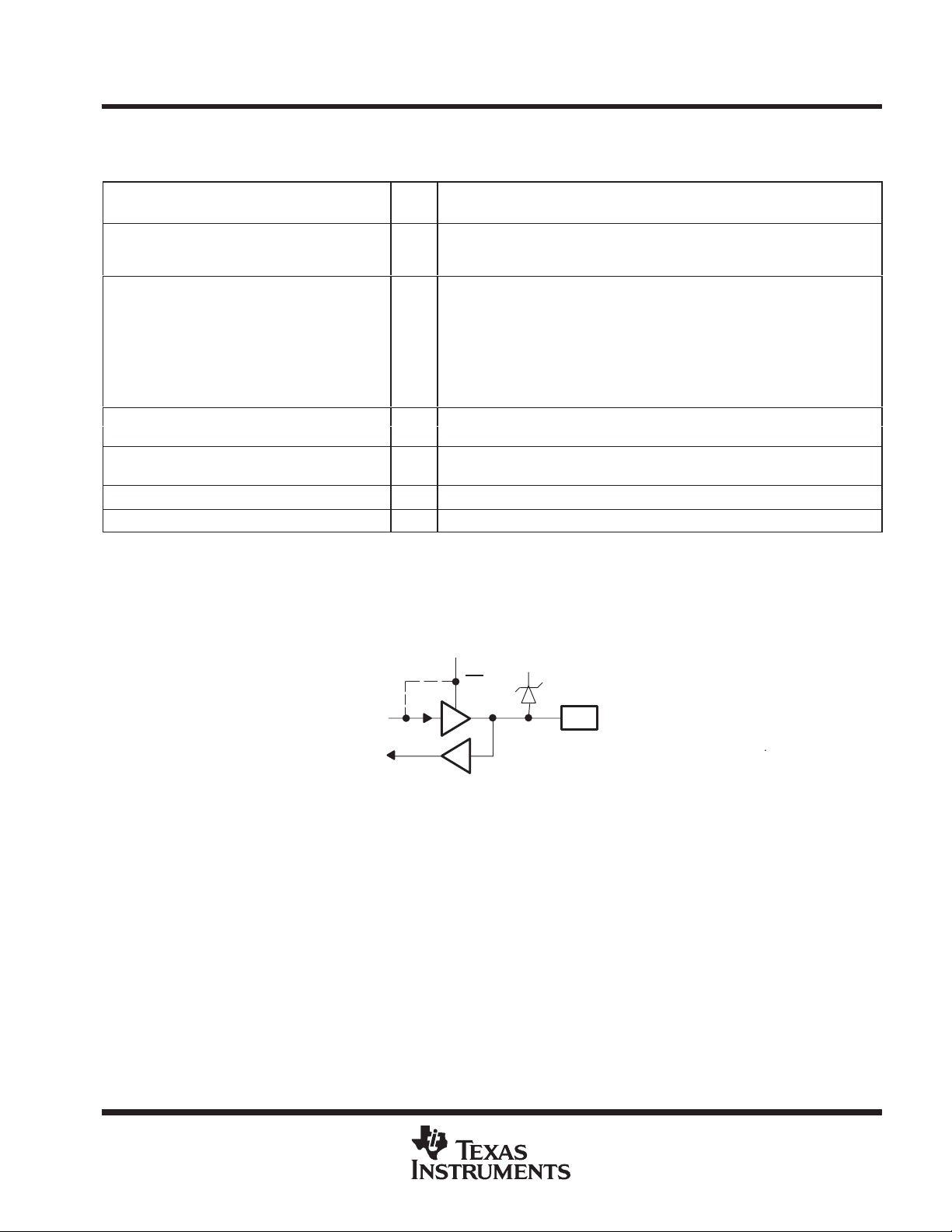
I/O characteristics
Figure 3 shows a 3-state bidirectional buffer illustration for reference. The table,
conditions
provides the electrical characteristics of the inputs and outputs. The PCI4450 meets the ac
specifications of the PC Card 95 Standard and the PCI Bus 2.1 specifications.
V
Tied for Open Drain
OE
CCP
recommended operating
Pad
Figure 3. 3-State Bidirectional Buffer
clamping voltages
The I/O sites can be pulled through a clamping diode to a voltage rail for protection. The 3.3-V core power supply
is independent of the clamping voltages. The clamping (protection) diodes are required if the signaling
environment on an I/O is system dependent. For example, PCI signaling can be either 3.3 Vdc or 5.0 Vdc, and
the PCI4450 must reliably accommodate both voltage levels. This is accomplished by using a 3.3-V buffer with
a clamping diode to V
the 5.0-V power supply.
A standard die has only one clamping voltage for the sites as shown in Figure 3. After the terminal assignments
are fixed, the fabrication facility will support a design by splitting the clamping voltage for customization. The
PCI4450 requires five separate clamping voltages since it supports a wide range of features. The five voltages
are listed and defined in the table,
. If a system design requires a 5.0-V PCI bus, then the V
CCP
recommended operating conditions
.
would be connected to
CCP
POST OFFICE BOX 655303 • DALLAS, TEXAS 75265
23

PCI4450 GFN/GJG
PC Card and OHCI Controller
SCPS046 – JANUAR Y 1999
PCI interface
This section describes the PCI interface of the PCI4450, and how the device responds to and participates in
PCI bus cycles. The PCI4450 provides all required signals for PCI master/slave devices and may operate in
either 5-V or 3.3-V PCI signaling environments by connecting the V
PCI bus lock (LOCK)
The bus locking protocol defined in the PCI Specification is not highly recommended, but is provided on the
PCI4450 as an additional compatibility feature. The PCI LOCK terminal is multiplexed with GPIO2, and the
terminal function defaults to a general-purpose input (GPI). The use of LOCK is only supported by
PCI-to-CardBus bridges in the downstream direction (away from the processor).
PCI LOCK indicates an atomic operation that may require multiple transactions to complete. When LOCK is
asserted, nonexclusive transactions may proceed to an address that is not currently locked. A grant to start
a transaction on the PCI bus does not guarantee control of LOCK; control of LOCK is obtained under its own
protocol. It is possible for different initiators to use the PCI bus while a single master retains ownership of LOCK.
To avoid confusion with the PCI bus clock, the CardBus signal for this protocol is CBLOCK.
An agent may need to do an exclusive operation because a critical memory access to memory might be broken
into several transactions, but the master wants exclusive rights to a region of memory. The granularity of the
lock is defined by PCI to be 16 bytes aligned. The lock protocol defined by PCI allows a resource lock without
interfering with nonexclusive, real-time data transfer, such as video.
terminals to the desired signaling level.
CCP
The PCI bus arbiter may be designed to support only complete bus locks using the LOCK protocol. In this
scenario the arbiter will not grant the bus to any other agent (other than the LOCK master) while LOCK is
asserted. A complete bus lock may have a significant impact on the performance of the video. The arbiter that
supports complete bus lock must grant the bus to the cache to perform a writeback due to a snoop to a modified
line when a locked operation is in progress.
The PCI4450 supports all LOCK protocol associated with PCI-to-PCI bridges, as also defined for
PCI-to-CardBus bridges. This includes disabling write posting while a locked operation is in progress, which
can solve a potential deadlock when using devices such as PCI-to-PCI bridges. The potential deadlock can
occur if a CardBus target supports delayed transactions and blocks access as the target until it completes a
delayed read. This target characteristic is prohibited by the 2.1 PCI Specification, and the issue is resolved by
the PCI master using LOCK.
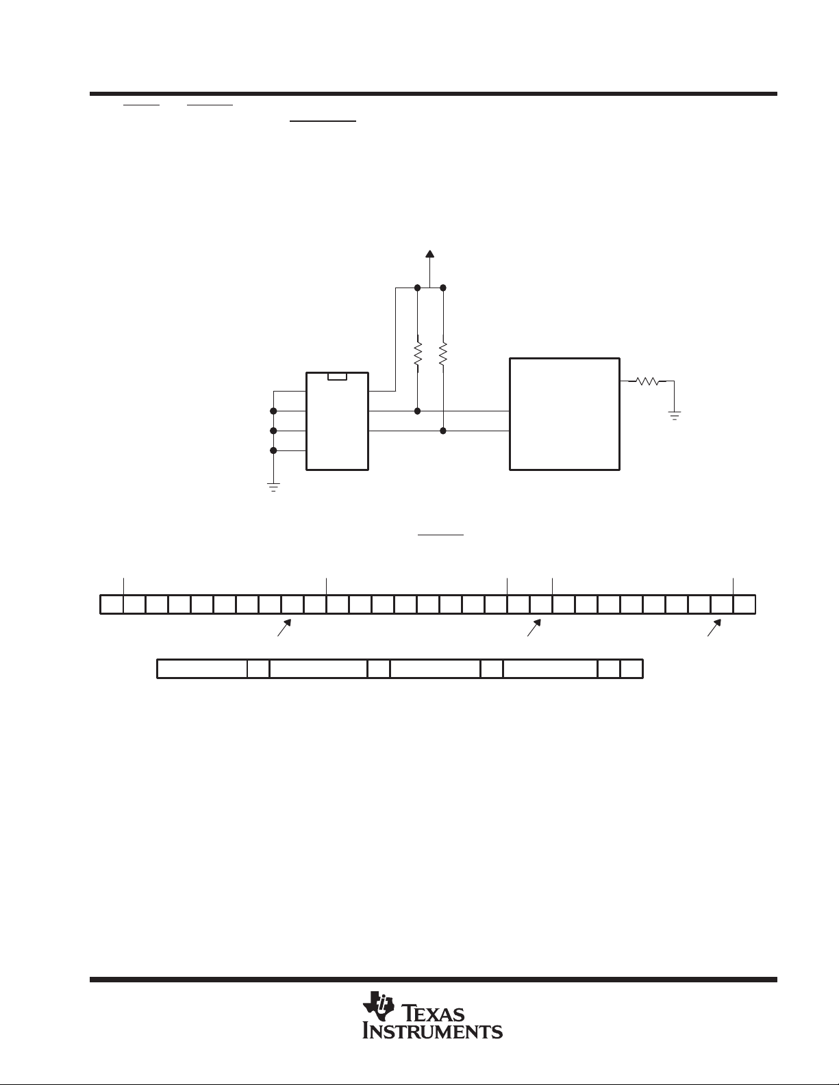
loading the subsystem identification (EEPROM interface)
The subsystem vendor ID register and subsystem ID register make up a double word of PCI configuration space
located at offset 40h for functions 0 and 1. This doubleword register, used for system and option card (mobile
dock) identification purposes, is required by some operating systems. Implementation of this unique identifier
register is a PC ‘97 requirement.
The PCI4450 offers two mechanisms to load a read-only value into the subsystem registers. The first
mechanism relies upon the system BIOS providing the subsystem ID value. The default access mode to the
subsystem registers is read-only, but the access mode may be made read/write by clearing the SUBSYSRW
bit in the system control register (bit 5 of the system control register, offset 80h). Once this bit is cleared (0),
the BIOS may write a subsystem identification value into the registers at offset 40h. The BIOS must set the
SUBSYSRW bit such that the subsystem vendor ID register and subsystem ID register are limited to read-only
access. This approach saves the added cost of implementing the serial EEPROM.
In some conditions, such as in a docking environment, the subsystem vendor ID register and subsystem ID
register must be loaded with a unique identifier through a serial EEPROM interface. The PCI4450 loads the
double-word of data from the serial EEPROM after a reset of the primary bus. The SUSPEND input gates the
24
POST OFFICE BOX 655303 • DALLAS, TEXAS 75265
PCI4450 GFN/GJG
PC Card and OHCI Controller
SCPS046 – JANUAR Y 1999
PRST and G_RST from the entire PCI4450 core, including the serial EEPROM state machine. Refer to
mode
for details on using SUSPEND. The PCI4450 provides a two-line serial bus interface to the serial
suspend
EEPROM.
The system designer must implement a pulldown resistor on the PCI4450 LATCH terminal to indicate the serial
EEPROM mode. Only when this pulldown resistor is present will the PCI4450 attempt to load data through the
serial EEPROM interface. The serial EEPROM interface is a two-pin interface with one data signal (SDA) and
one clock signal (SCL). Figure 4 illustrates a typical PCI4450 application using the serial EEPROM interface.
V
CC
Serial
EEPROM
A0
A1A2SCL
SDA
SCL
SDA
PCI4450
Latch
Figure 4. Serial EEPROM Application
As stated above, when the PCI4450 is reset by G_RST, the subsystem data is read automatically from the
EEPROM. The PCI4450 masters the serial EEPROM bus and reads four bytes as described in Figure 5.
Slave Address
S
b6 b5 b4 b3 b2 b1 b0 0 A b7 b6 b5 b4 b3 b2 b1 b0 A S b6 b5 b4 b3 b2 b1 b0 1 A
R/W# Restart R/W#
Data Byte 0 M PData Byte 1 M Data Byte 2 M Data Byte 3 M
S/P – Start/Stop Condition A – Slave Acknowledgment M – Master Acknowledgment
Word Address Slave Address
Figure 5. EEPROM Interface Subsystem Data Collection
The EEPROM is addressed at slave address A0h (1010 0000b), as indicated in Figure 5, and the EEPROM
word address auto-increments after each byte transfers according to the protocol. All hardware address bits
for the EEPROM should be tied to the appropriate level to achieve this slave address. Thus, to provide the
subsystem register with data AABBCCDDh the EEPROM should be programmed with address 0 = AAh, 1 =
BBh, 2 = CCh, and 3 = DDh.
The serial EEPROM chip in the sample application circuit, Figure 4, assumes the 1010b high address nibble.
The lower three address bits are terminal inputs to the chip, and the sample application shows these terminal
inputs tied to GND.
The serial EEPROM interface signals require pullup resistors. The serial EEPROM protocol allows bidirectional
transfers. Both the SCL and SDA signals are placed in a high-impedance state and pulled high when the bus
is not active. A high-to-low transition of the SDA line defines a start condition (S). A low-to-high transition of SDA
while SCL is high is defined as the stop condition (P). One bit is transferred during each clock pulse. The data
POST OFFICE BOX 655303 • DALLAS, TEXAS 75265
25
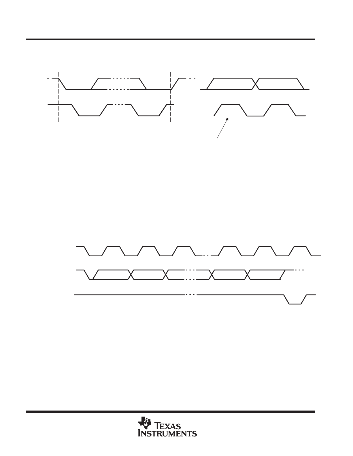
PCI4450 GFN/GJG
PC Card and OHCI Controller
SCPS046 – JANUAR Y 1999
on the SDA line must remain stable during the high period of the clock pulse, as changes in the data line at this
time will be interpreted as a control signal. Data is valid and stable during the clock high period. Figure 6
illustrates this protocol.
SDA
SCL
Start
Condition
Stop
Condition
Change of
Data Allowed
Data Line Stable,
Data Valid
Figure 6. Serial EEPROM Start/Stop Conditions and BIt Transfers
Each address byte and data transfer is followed by an acknowledge bit, as indicated in Figure 5. When the
PCI4450 transmits the addresses, it returns the SDA signal to the high state and places the line in a
high-impedance state. The PCI4450 then generates an SCL clock cycle and expects the EEPROM to pull down
the SDA line during the acknowledge pulse. This procedure is referred to as a slave acknowledge with the
PCI4450 transmitter and the EEPROM receiver. Figure 7 illustrates general acknowledges.
During the data byte transfers from the serial EEPROM to the PCI4450, the EEPROM clocks the SCL signal.
After the EEPROM transmits the data to the PCI4450, it returns the SDA signal to the high state and places
the line in a high-impedance state. The EEPROM then generates an SCL clock cycle and expects the PCI4450
to pull down the SDA line during the acknowledge pulse. This procedure is referred to as a master acknowledge
with the EEPROM transmitter and the PCI4450 receiver. Figure 7 illustrates general acknowledges.
SCL From
Master
SDA Output
By Transmitter
123 789
SDA Output
By Receiver
Figure 7. Serial EEPROM Protocol – Acknowledge
EEPROM interface status information is communicated through the general status register located at PCI offset
85h. The EEDETECT bit in this register indicates whether or not the PCI4450 serial EEPROM circuitry detects
the pulldown resistor on LATCH. An error condition, such as a missing acknowledge, results in the DAT AERR
bit being set. The EEBUSY bit is set while the subsystem ID register is loading (serial EEPROM interface is
busy).
26
POST OFFICE BOX 655303 • DALLAS, TEXAS 75265

PCI4450 GFN/GJG
PC Card and OHCI Controller
SCPS046 – JANUAR Y 1999
serial ROM implementation
A serial ROM interface exists in both the Open HCI function and the PC Card controller functions. The PCI4450
implementation adds a busy indication between the interfaces to allow the function 2 loading to follow the
functions 0 and 1 load. All serial ROM addressing uses slave address 8’hA0. The functions 0 and 1 serial
EEPROM state machine is modified to provide a busy indication to function 2 and to start loading registers at
word address 8’h20 to allow for some serial ROM format flexibility in function 2.
Primarily , the serial ROM is used to preload the PCI4450 registers with data, and only write accessible bits in
these registers may be preloaded. Figure 8 illustrates the PCI4450 serial ROM data format, which is an
expanded version of both the OHCI-Lynx and PCI1450 serial ROM formats.
Slave Address 8’b10100000 Flag byte Word address 32 (20h)
SubSys byte 3 Word address 33
MaxLat / MinGnt
SubSys byte 0
SubSys byte 1 Word address 2 SubSys byte 0 Word address 36
SubSys byte 2 Word address 3 SysCtrl byte 0 Word address 37
SubSys byte 3
Link_Enh byte 0 W ord address 5 SysCtrl byte 2 Word address 39
MiniROM_Addr W ord address 6 SysCtrl byte 3 Word address 40
GUIDHi byte 0
GUIDHi byte 1
GUIDHi byte 2
GUIDHi byte 3 Word address 10 MF route byte 0 Word address 44
GUIDLo byte 0 W ord address 1 1 MF route byte 1 Word address 45
GUIDLo byte 1
GUIDLo byte 2 Word address 13 MF route byte 3 Word address 47
GUIDLo byte 3 Word address 14 Card Control Word address 48
CheckSum
Link_Enh byte 1 Word address 16 Diagnostic Word address 50
PCI misc byte 0 Word address 17 PMC byte 1 Word address 51
PCI misc byte 1
RSVD
Word address 0
Word address 1
Word address 4
Word address 7
Word address 8
Word address 9
Word address 12
Word address 15
Word address 18
SubSys byte 2 Word address 34
SubSys byte 1 Word address 35
SysCtrl byte 1 Word address 38
General control Word address 41
GP event enable Word address 42
GP output Word address 43
MF route byte 2 Word address 46
Device control Word address 49
ExCA ID and rev Word address 52
...
AVAIL
Figure 8. Serial ROM Data Format
The flag byte at word address 32 indicates to the PCI4450 whether or not the PC Card controller functions loads
the data from word address range 33–52. A flag byte set to 8’hFF indicates to stop loading the serial ROM data
for functions 0 and 1, but is independent of the function 2 1394 Open HCI controller load from word address
range 0–18.
An additional change in the serial ROM behavior with respect to Open HCI GUIDROM register access is the
MiniROM_Addr. The MiniROM_Addr field in the ROM data is loaded from byte location 6 (EEPROM word
address 6) and indicates to function 2 where to begin accessing the serial ROM via the GUID ROM register.
The GUIDROM.addrReset bit function changes slightly to reset serial ROM access to the byte location
indicated by MiniROM_Addr. A MiniROM_Addr value of zero provides identical operation as the OHCI-Lynx.
POST OFFICE BOX 655303 • DALLAS, TEXAS 75265
27
PCI4450 GFN/GJG
PC Card and OHCI Controller
SCPS046 – JANUAR Y 1999
PC Card applications overview
This section describes the PC Card interfaces of the PCI4450. A discussion on PC Card recognition details the
card interrogation procedure. This section discusses the card powering procedure, including the protocol of the
P2C power switch interface. The internal ZV buffering provided by the PCI4450 and programming model is
detailed in this section. Also, standard PC Card register models are described, as well as a brief discussion of
the PC Card software protocol layers.
PC Card insertion/removal and recognition
The 1995 PC Card Standard addresses the card detection and recognition process through an interrogation
procedure that the socket must initiate upon card insertion into a cold, unpowered socket. Through this
interrogation, card voltage requirements and interface (16-bit vs. CardBus) are determined.
The scheme uses the CD1, CD2, VS1, and VS2 signals (CCD1, CCD2, CVS1, CVS2 for CardBus). A PC Card
designer connects these four pins in a certain configuration depending on the type of card and the supply
voltage. The encoding scheme for this, defined in the 1997 PC Card Standard, is shown in Table 18.
Table 18. PC Card – Card Detect and Voltage Sense Connections
CD2//CCD2 CD1//CCD1 VS2//CVS2 VS1//CVS1 Key Interface Voltage
Ground Ground Open Open 5 V 16-bit PC Card 5 V
Ground Ground Open Ground 5 V 16-bit PC Card 5 V and 3.3 V
Ground Ground Ground Ground 5 V 16-bit PC Card
Ground Ground Open Ground LV 16-bit PC Card 3.3 V
Ground Connect to CVS1 Open Connect to CCD1 LV CardBus PC Card 3.3 V
Ground Ground Ground Ground LV 16-bit PC Card 3.3 V and X.X V
Connect to CVS2 Ground Connect to CCD2 Ground LV CardBus PC Card 3.3 V and X.X V
Connect to CVS1 Ground Ground Connect to CCD2 LV CardBus PC Card
Ground Ground Ground Open LV 16-bit PC Card Y.Y V
Connect to CVS2 Ground Connect to CCD2 Open LV CardBus PC Card Y .Y V
Ground Connect to CVS2 Connect to CCD1 Open LV CardBus PC Card X.X V and Y.Y V
Connect to CVS1 Ground Open Connect to CCD2 LV CardBus PC Card Y.Y V
Ground Connect to CVS1 Ground Connect to CCD1 Reserved
Ground Connect to CVS2 Connect to CCD1 Ground Reserved
5 V , 3.3 V, and
X.X V
3.3 V, X.X V , and
Y.Y V
P2C power switch interface (TPS2202A/2206)
A power switch with a PCMCIA-to-peripheral control (P2C) interface is required for the PC Card powering
interface. The TI TPS2206 (or TPS2202A) Dual-Slot PC Card Power-Interface Switch provides the P2C
interface to the CLOCK, DA TA, and LA TCH terminals of the PCI4450. Figure 9 shows the terminal assignments
of the TPS2206. Figure 10 illustrates a typical application where the PCI4450 represents the PCMCIA
controller.
There are two ways to provide a clock source to the power switch interface. The first method is to provide an
external clock source such as a 32 kHz real time clock to the CLOCK terminal. The second method is to use
the internal ring oscillator. If the internal ring oscillator is used, then the PCI4450 provides its own clock source
for the PC Card interrogation logic and the power switch interface. The mode of operation is determined by the
setting of bit 27 of the system control register (PCI offset 80h). This bit is encoded as follows:
0 = CLOCK terminal (terminal U12) is an input (default).
1 = CLOCK terminal is an output that utilizes the internal oscillator.
28
POST OFFICE BOX 655303 • DALLAS, TEXAS 75265
A 43 kW pulldown resistor should be tied to the CLOCK pin.
PCI4450 GFN/GJG
PC Card and OHCI Controller
SCPS046 – JANUAR Y 1999
Power Supply
12 V
5 V
3.3 V
5V
5V
DATA
CLOCK
LATCH
RESET
12V
AVPP
AVCC
AVCC
AVCC
GND
NC
RESET
3.3V
NC – No internal connection
1
2
3
4
5
6
7
8
9
10
11
12
13
14
15
30
29
28
27
26
25
24
23
22
21
20
19
18
17
16
5V
NC
NC
NC
NC
NC
12V
BVPP
BVCC
BVCC
BVCC
NC
OC
3.3V
3.3V
Figure 9. TPS2206 Terminal Assignments
TPS2206
12 V
5 V
3.3 V
AVPP
AVCC
AVCC
AVCC
PC Card A
V
PP1
V
PP2
V
CC
V
CC
Supervisor
PCI4450
3
RESET
BVPP
BVCC
Serial I/F
PC Card Interface (68 pins/socket)
BVCC
BVCC
PC Card B
V
PP1
V
PP2
V
CC
V
CC
Figure 10. TPS2206 Typical Application
zoomed video support
The zoomed video (ZV) port on the PCI4450 provides an internally buffered 16-bit ZV PC Card data path. This
internal routing is programmed through the multimedia control register. Figure 10 summarizes the zoomed
video subsystem implemented in the PCI4450, and details the bit functions found in the multimedia control
register.
POST OFFICE BOX 655303 • DALLAS, TEXAS 75265
29
PCI4450 GFN/GJG
PC Card and OHCI Controller
SCPS046 – JANUAR Y 1999
An output port (PORTSEL) is always selected. The PCI4450 defaults to socket 0 (see the multimedia control
register). When ZVOUTEN is enabled, the zoomed video output terminals are enabled and allow the PCI4450
to route the zoomed video data. However, no data is transmitted unless either ZVEN0 or ZVEN1 is enabled
in the multimedia control register. If the PORTSEL maps to a card port that is disabled (ZVEN =0 or ZVEN1
= 0), then the zoomed video port is driven low (i.e., no data is transmitted).
Zoomed Video Subsystem
Card Output
Enable Logic
ZVEN0
ZVOUTEN
PC Card
Socket 0
PC Card
Socket 1
Card Output
Enable Logic
†
ZVST A T must be enabled through the GPIO Control Register .
PC Card
I/F
PC Card
I/F
ZVEN1
23
PORTSEL
ZVST AT†
19 Video Signals
4 Audio Signals
VGA
Audio
Codec
Figure 11. Zoomed Video Subsystem
zoomed video auto detect
Zoomed video auto detect, when enabled, allows the PCI4450 to automatically detect zoomed video data by
sensing the pixel clock from each socket and/or from a third zoomed video source that may exist on the
motherboard. The PCI4450 automatically switches the internal zoomed video MUX to route the zoomed video
stream to the PCI4450’s zoomed video output port. This eliminates the need for software to switch the internal
MUX using the multimedia control register (PCI offset 84h, bits 6 and 7).
The PCI4450 can be programmed to switch a third zoomed video source by programming MFUNC2 or
MFUNC3 as a zoomed video pixel clock sense pin and connecting this pin to the pixel clock of the third zoomed
video source. ZVSTAT may then be programmed onto MFUNC4, MFUNC1, or MFUNC0 and this signal may
switch the zoomed video buffers from the third zoomed video source. To account for the possibility of several
zoomed video sources being enabled at the same time, a programmable priority scheme may be enabled.
30
POST OFFICE BOX 655303 • DALLAS, TEXAS 75265

Zoomed Video Subsystem
Card Output
Enable Logic
ZVEN0
Pixel Clock Sense
Programmed on
MFUNC2 or MFUNC3
PCI4450 GFN/GJG
PC Card and OHCI Controller
SCPS046 – JANUAR Y 1999
3rd Zoomed Video Source
23
PC Card
Socket 0
PC Card
Socket 1
PC Card
I/F
23
Pixel Clock Sense
23
23
Pixel Clock Sense
23
Card Output
Enable Logic
Auto Z/V Arbiter
and Buffer
PC Card
I/F
ZVEN1
ZVST AT
23
ZV Data
Enable
19 Video Signals
4 Audio Signals
Figure 12. Zoomed Video with Auto Detect Enabled
Buffers
23
VGA
Audio
Codec
The PCI4450 defaults with zoomed video auto-detect disabled so that it will function exactly like the PCI1250A
and PCI1450. To enable zoomed video auto-detect and the programmable priority scheme, the following bits
must be set:
D Multimedia control register (PCI offset 84h) bit 5: Writing a 1b enables zoomed video auto-detect
D Multimedia control register (PCI offset 84h) bits 4–2: Set the programmable priority scheme
000 = Slot A, Slot B, External Source
001 = Slot A, External Source, Slot B
010 = Slot B, Slot A, External Source
011 = Slot B, External Source, Slot A
100 = External Source, Slot A, Slot B
101 = External Source, Slot B, Slot A
110 = External Source, Slot B, Slot A
111 = Reserved
POST OFFICE BOX 655303 • DALLAS, TEXAS 75265
31

PCI4450 GFN/GJG
PC Card and OHCI Controller
SCPS046 – JANUAR Y 1999
If it is desired to switch a third zoomed video source, then the following bits must also be set:
D MFUNC routing register (PCI offset 8Ch), bits 14–12 or 10–8: Write 11 1b to program MFUNC3 or MFUNC2
as a pixel clock input pin.
D MFUNC routing register (PCI ofset 8Ch), bits 18–16, 6–4, or 2–0: Write 111b to program MFUNC4,
MFUNC1, or MFUNC0 pin.
ultra zoomed video
Ultra zoomed video is an enhancement to the PCI4450’s DMA engine and is intended to improve the 16-bit
bandwidth for MPEG I and MPEG II decoder PC Cards. This enhancement allows the 4450 to fetch 32 bits of
data from memory versus the 1 1XX/12XX 16-bit fetch capability. This enhancement allows a higher sustained
throughput to the 16-bit PC Card, because the 4450 prefetches an extra 16 bits (32 bits total) during each PCI
read transaction. If the PCI Bus becomes busy, then the 4450 has an extra 16 bits of data to perform
back-to-back 16-bit transactions to the PC Card before having to fetch more data. This feature is built into the
DMA engine and software is not required to enable this enhancement.
NOTE:The 11XX and 12XX series CardBus controllers have enough 16-bit bandwidth to support
MPEG II PC Card decoders. But it was decided to improve the bandwidth even more in the 14XX
series CardBus controllers.
D3_STAT pin
Additional functionality added for the 4450 versus the 1250A/1251 series is the D3_ST A T (D3 status) pin. This
pin is asserted under the following two conditions (both conditions must be true before D3_STA T is asserted):
D Function 0 and Function 1 are placed in D3
D PME is enabled on either function
The intent of including this feature in the PCI4450 is to use this pin to switch an external VCC/V
feature can be programmed on MFUNC7, MFUNC6, MFUNC2, or MFUNC1 by writing 100b to the appropriate
multifunction routing status register bits (PCI offset 8Ch).
internal ring oscillator
The internal ring oscillator provides an internal clock source for the PCI4450 so that neither the PCI clock nor
an external clock is required in order for the PCI4450 to power down a socket or interrogate a PC Card. This
internal oscillator operates nominally at 16 kHz and can be enabled by setting bit 27 of the system control
register (PCI offset 80h) to a 1b. This function is disabled by default.
SPKROUT usage
The SPKROUT signal carries the digital audio signal from the PC Card to the system. When a 16-bit PC Card
is configured for I/O mode, the BVD2 pin becomes SPKR. This terminal, also used in CardBus applications,
is referred to as CAUDIO. SPKR passes a TTL level digital audio signal to the PCI4450. The CardBus CAUDIO
signal also can pass a single amplitude, binary waveform. The binary audio signals from the two PC Card
sockets are XOR’ed in the PCI4450 to produce SPKROUT. Figure 13 illustrates the SPKROUT connection.
Bit 1, Card Control Register (offset 91h)
Card A SPKROUT Enable
Card A SPKR
SPKROUT
Bit 1, Card Control Register (offset 91h)
Card B SPKROUT Enable
Card B SPKR
AUX
switch. This
Speaker
Driver
32
Card A SPKROUT Enable
Card B SPKROUT Enable
Figure 13. SPKROUT Connection to Speaker Driver
POST OFFICE BOX 655303 • DALLAS, TEXAS 75265

PCI4450 GFN/GJG
PC Card and OHCI Controller
SCPS046 – JANUAR Y 1999
The SPKROUT signal is typically driven only by PC modem cards. To verify the SPKROUT on the PCI4450,
a sample circuit was constructed, and this simplified schematic is provided below. The PCI1130/1131 required
a pullup resistor on the SUSPEND/SPKROUT terminal. Since the PCI4450 does not multiplex any other
function on SPKROUT, this terminal does not require a pullup resistor.
V
CC
V
CC
SPKROUT
Figure 14. Simplified Test Schematic
LED socket activity indicators
3
7
2
6
+
–
4
LM386
1
8
Speaker
The socket activity LEDs indicate when an access is occurring to a PC Card. The LED signals are
programmable via the MFUNC register. When configured for LED outputs, these terminals output an active high
signal to indicate socket activity. LEDA1 indicates socket 0 (card A) activity, and LEDA2 indicates socket 1
(card B) activity.
The active-high LED signal is driven for 64 ms durations. When the LED is not being driven high, then it is driven
to a low state. Either of the two circuits illustrated in Figure 15 can be implemented to provide the LED signaling,
and it is left for the board designer to implement the circuit to best fit the application.
Current Limiting
R ≈ 500 Ω
PCI4450
PCI4450
Application-
Specific Delay
Current Limiting
R ≈ 500 Ω
LED
LED
Figure 15. Two Sample LED Circuits
As indicated, the LED signals are driven for 64 ms, and this is accomplished by a counter circuit. T o avoid the
possibility of the LEDs appearing to be stuck when the PCI clock is stopped, the LED signaling is cut off when
either the SUSPEND signal is asserted or when the PCI clock is to be stopped per the CLKRUN protocol.
Furthermore, if any additional socket activity occurs during this counter cycle, then the counter is reset and the
LED signal remains driven. If socket activity is frequent (at least once every 64 ms), then the LED signals will
remain driven.
POST OFFICE BOX 655303 • DALLAS, TEXAS 75265
33

PCI4450 GFN/GJG
PC Card and OHCI Controller
SCPS046 – JANUAR Y 1999
PC Card 16 DMA support
The PCI4450 supports both PC/PCI (centralized) DMA and a distributed DMA slave engine for 16-bit PC Card
DMA support. The distributed DMA (DDMA) slave register set provides the programmability necessary for the
slave DDMA engine. Table 19 provides the DDMA register configuration.
Table 19. Distributed DMA Registers
TYPE REGISTER NAME
R
W
R
W
R N/A
W Mode
R Multichannel
W Mask
Reserved Page
Reserved Reserved
Reserved
Reserved
N/A Status 08h
Request Command
N/A
Master Clear
Current address 00h
Base address
Current count 04h
Base count
Reserved
DMA BASE
ADDRESS OFFSET
CardBus socket register
The PCI4450 contains all registers for compatibility with the latest PCI to PCMCIA CardBus Bridge
Specification. These registers exist as the CardBus socket registers, and are listed in Table 20.
Table 20. CardBus Socket Registers
REGISTER NAME OFFSET
Socket event 00h
Socket mask 04h
Socket present state 08h
Socket force event 0Ch
Socket control 10h
Reserved 14h
Reserved 18h
Reserved 1Ch
Socket power management 20h
0Ch
34
POST OFFICE BOX 655303 • DALLAS, TEXAS 75265

PCI4450 GFN/GJG
PC Card and OHCI Controller
SCPS046 – JANUAR Y 1999
programmable interrupt subsystem
Interrupts provide a way for I/O devices to let the microprocessor know that they require servicing. The dynamic
nature of PC Cards, and the abundance of PC Card I/O applications require substantial interrupt support from
the PCI4450. The PCI4450 provides several interrupt signaling schemes to accommodate the needs of a
variety of platforms. The different mechanisms for dealing with interrupts in this device are based upon various
specifications and industry standards. The ExCA register set provides interrupt control for some 16-bit PC Card
functions, and the CardBus socket register set provides interrupt control for the CardBus PC Card functions.
The PCI4450 is therefore backward compatible with existing interrupt control register definitions, and new
registers have been defined where required.
The PCI4450 detects PC Card interrupts and events at the PC Card interface and notifies the host controller
via one of several interrupt signaling protocols. T o simplify the discussion of interrupts in the PCI4450, PC Card
interrupts are classified as either card status change (CSC) or as functional interrupts.
The method by which any type of PCI4450 interrupt is communicated to the host interrupt controller varies from
system to system. The PCI4450 offers system designers the choice of using parallel PCI interrupt signaling or
the serialized ISA and/or PCI interrupt protocol. It is possible to use the parallel PCI interrupts in combination
with serialized IRQs via the multifunction routing register at offset 8Ch.
PC Card functional and card status change interrupts
PC Card functional interrupts are defined as requests from a PC Card application for interrupt service. They
are indicated by asserting specially defined signals on the PC Card interface. Functional interrupts are
generated by 16-bit I/O PC Cards and by CardBus PC Cards.
Card status change (CSC) type interrupts, defined as events at the PC Card interface which are detected by
the PCI4450, may warrant notification of host card and socket services software for service. CSC events include
both card insertion and removal from PC Card sockets, as well as transitions of certain PC Card signals.
Table 21 summarizes the sources of PC Card interrupts and the type of card associated with them. CSC and
functional interrupt sources are dependent upon the type of card inserted in the PC Card socket. The three types
of cards that may be inserted into any PC Card socket are: 16-bit memory card, 16-bit I/O card, and CardBus
cards. Functional interrupt events are valid only for 16-bit I/O and CardBus cards, that is, the functional
interrupts are not valid for 16-bit memory cards. Furthermore, card insertion and removal type CSC interrupts
are independent of the card type.
POST OFFICE BOX 655303 • DALLAS, TEXAS 75265
35

PCI4450 GFN/GJG
BVD1 (STSCHG) //
A transition on the BVD1 signal indicates a change
Battery conditions
y
All PC Cards
PC Card and OHCI Controller
SCPS046 – JANUAR Y 1999
Table 21. PC Card Interrupt Events and Description
Card T ype Event Type Signal Description
BVD1 (STSCHG) // A transition on the BVD1 signal indicates a change
CSTSCHG
BVD1 (STSCHG) //
CSTSCHG
BVD1 (STSCHG) //
CSTSCHG
CD1 // CCD1,
CD2 // CCD2
in the PC Card battery conditions.
A transition on the BVD2 signal indicates a change
in the PC Card battery conditions.
A transition on the READY signal indicates a change
in the ability of the memory PC Card to accept or
provide data.
The assertion of the STSCHG signal indicates a
status change on the PC Card.
The assertion of the IREQ signal indicates an
interrupt request from the PC Card.
The assertion of the CSTSCHG signal indicates a
status change on the PC Card.
The assertion of the CINT signal indicates an
interrupt request from the PC Card.
An interrupt is generated when a PC Card power-up
cycle has completed.
A transition on either the CD1//CCD1 signal or the
CD2//CCD2 signal indicates an insertion or removal
of a 16-bit // CardBus PC Card.
An interrupt is generated when a PC Card power-up
cycle has completed.
16-bit Memory
16-bit I/O
CardBus
All PC Cards
Battery conditions
(BVD1, BVD2)
Wait states
(READY)
Change in card status
(STSCHG)
Interrupt request
(IREQ)
Change in card status
(CSTSCHG)
Interrupt request
(CINT)
Power cycle complete CSC N/A
Card insertion or
removal
Power cycle complete CSC N/A
CSC
CSC BVD2 (SPKR) // CAUDIO
CSC READY (IREQ) // CINT
CSC
Functional READY (IREQ) // CINT
CSC
Functional READY (IREQ) // CINT
CSC
The signal naming convention for PC Card signals describes the function for 16-bit memory and I/O cards, as
well as CardBus. For example, the READY(IREQ)//CINT signal includes the READY signal for 16-bit memory
cards, the IREQ signal for 16-bit I/O cards, and the CINT signal for CardBus cards. The 16-bit memory card
signal name is first, with the I/O card signal name second enclosed in parentheses. The CardBus signal name
follows after a forward double slash (//).
The PC Card standard describes the power-up sequence that must be followed by the PCI4450 when an
insertion event occurs and the host requests that the socket VCC and VPP be powered. Upon completion of this
power-up sequence, the PCI4450 interrupt scheme may be used to notify the host system, as in indicated in
Table 21, denoted by the power cycle complete event. This interrupt source is considered a PCI4450 internal
event because it does not depend on a signal change at the PC Card interface, but rather the completion of
applying power to the socket.
interrupt masks and flags
Host software may individually mask, or disable, most of the potential interrupt sources listed in Table 22 by
setting the appropriate bits in the PCI4450. By individually masking the interrupt sources listed in these tables,
software can control which events will cause a PCI4450 interrupt. Host software has some control over which
system interrupt the PCI4450 will assert by programming the appropriate routing registers. The PCI4450 allows
host software to route PC Card CSC and PC Card functional interrupts to separate system interrupts. Interrupt
routing is somewhat specific to the interrupt signaling method used. This will be discussed in more detail in the
following sections.
When an interrupt is signaled by the PCI4450, the interrupt service routine must be able to discern which of
the events in Table 22 caused the interrupt. Internal registers in the PCI4450 provide flags which report which
of the interrupt sources was the cause of an interrupt. By reading these status bits, the interrupt service routine
can determine which action is to be taken.
36
POST OFFICE BOX 655303 • DALLAS, TEXAS 75265
PCI4450 GFN/GJG
B
ExCA Off
h/45h/805h
ExCA Off
04h/44h/804h
PC Card and OHCI Controller
SCPS046 – JANUAR Y 1999
Table 22 details the registers and bits associated with masking and reporting potential interrupts. All interrupts
may be masked except the functional PC Card interrupts, and an interrupt status flag is available for all types
of interrupts.
Table 22. PCI4450 Interrupt Masks and Flags Registers
Card T ype Event Mask Flag
attery conditions
16-bit Memory
16-bit I/O
All 16-bit PC Cards Power cycle complete
CardBus
(BVD1, BVD2) Bits 1 & 0 Bits 1 & 0
Wait states
(READY)
Change in card status
(STSCHG)
Interrupt request
(IREQ)
Change in card status
(CSTSCHG)
Interrupt request
(CINT)
Power cycle complete
Card insertion or removal
ExCA Offset 05h/45h/805h
ExCA Offset 05h/45h/805h
ExCA Offset 05h/45h/805h
set 05
Bit 2
Bit 0
Always enabled
Bit 3
Socket mask register
Bit 0
Always enabled
Socket mask register
Bit 3
Socket mask register
Bits 2 & 1
set
ExCA Offset 04h/44h/804h
Bit 2
ExCA Offset 04h/44h/804h
Bit 0
PCI Configuration Offset 91h
Bit 0
ExCA Offset 04h/44h/804h
Bit 3
Socket event register
Bit 0
PCI Configuration Offset 91h
Bit 0
Socket event register
Bit 3
Socket event register
Bits 2 & 1
There is no mask bit to stop the PCI4450 from passing PC Card functional interrupts through to the appropriate
interrupt scheme. Functional interrupts should not be fired until the PC Card is initialized and powered.
There are various methods of clearing the interrupt flag bits listed in Table 22. The flag bits in the ExCA registers
(16-bit PC Card related interrupt flags) may be cleared by two different methods. One method is an explicit write
of 1 to the flag bit to clear, and the other is a reading of the flag bit register. The selection of flag bit clearing
is made by bit 2 in the global control register (ExCA offset 1Eh/5Eh/81Eh), and defaults to the flag cleared on
read method.
The CardBus related interrupt flags can only be cleared by an explicit write of 1 to the interrupt flag in the socket
event register. Although some of the functionality is shared between the CardBus registers and the ExCA
registers, software should not program the chip through both register sets when a CardBus card is functioning.
using parallel PCI interrupts
Parallel PCI interrupts are available when in pure parallel PCI interrupt mode and are routed on
MFUNC0–MFUNC2. The PCI interrupt signaling is dependent upon the interrupt mode and is summarized in
Table 23. The interrupt mode is selected in the device control register (92h).
Table 23. Interrupt Pin Register Cross Reference
Interrupt Signaling Mode
Parallel PCI interrupts only 0x01 (INTA) 0x02 (INTB)
Reserved 0x01 (INTA) 0x02 (INTB)
IRQ serialized (IRQSER) & parallel PCI interrupts 0x01 (INTA) 0x01 (INTA)
IRQ & PCI serialized (IRQSER) interrupts (default) 0x01 (INTA) 0x02 (INTB)
INTPIN
Function 0
INTPIN
Function 1
POST OFFICE BOX 655303 • DALLAS, TEXAS 75265
37

PCI4450 GFN/GJG
PC Card and OHCI Controller
SCPS046 – JANUAR Y 1999
power management overview
In addition to the low-power CMOS technology process used for the PCI4450, various features are designed
into the device to allow implementation of popular power saving techniques. These features and techniques
are discussed in this section.
CLKRUN protocol
CLKRUN is the primary method of power management on the PCI bus side of the PCI4450. Since some
chipsets do not implement CLKRUN, this is not always available to the system designer, and alternate power
savings features are provided.
If CLKRUN is not implemented, then the CLKRUN pin should be tied low. CLKRUN is enabled by default via
bit 1 (KEEPCLK) in the system control register (80h).
CardBus PC Card power management
The PCI4450 implements its own card power management engine that can turn off the CCLK to a socket when
there is no activity to the CardBus PC Card. The CCLK can also be configured as divide by 16 instead of
stopped. The CLKRUN protocol is followed on the CardBus interface to control this clock management.
PCI bus power management
The
PCI Bus Power Management Interface Specification
the operating system control the power of PCI functions. This is done by defining a standard PCI interface and
operations to manage the power of PCI functions on the bus. The PCI bus and the PCI functions can be
assigned one of four software visible power management states, which result in varying levels of power savings.
(PCIPM) establishes the infrastructure required to let
The four power management states of PCI functions are: D0 - Fully On state, D1 and D2 - intermediate states,
and D3 - Off state. Similarly, bus power states of the PCI bus are B0–B3. The bus power states B0–B3 are
derived from the device power state of the upstream bridge device.
For the operating system to manage the device power states on the PCI bus, the PCI function should support
four power management operations. The four operations are: capabilities reporting; power status reporting;
setting the power state; and system wake-up. The operating system identifies the capabilities of the PCI
function by traversing the new capabilities list. The presence of new capabilities is indicated by a 1b in bit 4 of
the PCI status register (PCI offset 06h). When software determines that the device has a capabilities list by
seeing that bit 4 of the PCI status register is set, it will read the capability pointer register at PCI offset 14h. This
value in the register points the location in PCI configuration space of the capabilities linked list.
The first byte of each capability register block is required to be a unique ID of that capability. PCI power
management has been assigned an ID of 01h. The next byte is a pointer to the next pointer item in the list of
capabilities. If there are no more items in the list, then the next item pointer should be set to 0. The registers
following the next item pointer are specific to the function’s capability. The PCIPM capability implements the
following register block:
Power Management Register Block
Power management capabilities (PMC) Next item pointer Capability ID Offset = 0
Data
PMCSR bridge
support extensions
Power management control status (CSR) Offset = 4
The power management capabilities (PMC) register is a static read-only register that provides information on
the capabilities of the function, related to power management. The PMCSR register enables control of power
management states and enables/monitors power management events. The data register is an optional register
that provides a mechanism for state-dependent power measurements such as power consumed or heat
dissipation.
38
POST OFFICE BOX 655303 • DALLAS, TEXAS 75265

PC Card and OHCI Controller
CardBus device class power management
The
PCI Bus Interface Specification for PCI-to-CardBus Bridges
1997. This specification follows the device and bus state definitions provided in the
Management Interface Specification
addressed in the
without losing wake-up context (also called PME context).
PCI Bus Interface Specification for PCI-to-CardBus Bridges
published by the PCI Special Interest Group (SIG). The main issue
was approved by PCMCIA in December of
is wake-up from D3
PCI4450 GFN/GJG
SCPS046 – JANUAR Y 1999
PCI Bus Power
or D3
hot
cold
The specific issues addressed by the
up are as follows:
D Preservation of device context: The
must be asserted when transitioning from D3
be implemented so that PRST does not clear the PME context registers.
D Power source in D3
The Texas Instruments PCI4450 addresses these D3 wake-up issues in the following manner:
if wake-up support is required from this state.
cold
PCI Bus Interface Specification for PCI-to-CardBus Bridges
PCI Power Management Specification
to D0. Some method to preserve wake-up context must
cold
version 1.0 states that PRST
D Preservation of device context: When PRST is asserted, bits required to preserve PME context are not
cleared. To clear all bits in the PCI4450, another reset pin is defined: G_RST (global reset). G_RST is
normally only asserted during the initial power-on sequence. After the initial boot, PRST should be asserted
so that PME context is retained for D3-to-D0 transitions. Bits cleared by G_RST, but not cleared by PRST
(if the PME enable bit is set), are referred to as PME context bits. Please refer to the master list of PME
context bits in the next section.
D Power source in D3
auxiliary power source must be switched to the PCI4450 VCC pins. This switch should be a
break
type of switch, so that VCC to the PCI4450 is not interrupted.
master list of PME context bits and global reset only bits
PME context bit means that the bit is cleared only by the assertion of G_RST when the PME enable bit is set
(PCI offset A4h, bit 8). If PME is not enabled, then these bits are cleared when either PRST or G_RST is
asserted.
Global reset only bits, as the name implies, are only cleared by G_RST. These bits are never cleared by PRST
regardless of the setting of the PME enable bit. (PCI offset A4h, bit 8). The G_RST signal is gated only by the
SUSPEND signal. This means that assertion of SUSPEND blocks the G_RST signal internally, thus preserving
all register contents.
if wake-up support is required from this state. Since VCC is removed in D3
cold
for D3 wake
, an
cold
make before
POST OFFICE BOX 655303 • DALLAS, TEXAS 75265
39

PCI4450 GFN/GJG
PC Card and OHCI Controller
SCPS046 – JANUAR Y 1999
Global reset only bits:
D Subsystem ID/subsystem vendor ID (PCI offset 40h): bits 31–0
D PC Card 16-bit legacy mode base address register (PCI offset 44h): bits 31–1
D System control register (PCI offset 80h): bits 31–29, 27–24, 22–14, 6–3, 1, 0
D Multimedia control register (PCI offset 84h): bits 7–0
D General status register (PCI offset 85h): bits 2–0
D General-purpose event status register (PCI offset 88h): bits 7, 6, 3–0
D General-purpose event enable register (PCI offset 89h): bits 7, 6, 3–0
D General-purpose input register (PCI offset 8Ah): bits 3–0
D General-purpose output register (PCI offset 8Bh): bits 3–0
D MFUNC routing register (PCI offset 8Ch): bits 31–0
D Retry status register (PCI offset 90h): bits 7–1
D Card control register (PCI offset 91h): bits 7, 6, 2, 1, 0
D Device control register (PCI offset 92h): bits 7–0
D Diagnostic register (PCI offset 93h): bits 7–0
D Socket DMA register 0 (PCI offset 94h): bits 1–0
D Socket DMA register 1 (PCI offset 98h): bits 15–0
D GPE control/status register (PCI offset A8h): bits 10, 9, 8, 2, 1, 0
PME context bits
D Bridge control register (PCI offset 3Eh): bit 6
D Power management capabilities register (PCI offset A2h): bit 15
D Power management control/status register (PCI offset A4h): bits 15, 8
D ExCA power control register (ExCA 802h/842h): bits 7, 4, 3, 1, 0
D ExCA interrupt and general control (ExCA 803h/843h): bit 6, 5
D ExCA card status change register (ExCA 804h/844h): bits 3–0
D ExCA card status change interrupt register (ExCA 805h/845h): bits 3–0
D CardBus socket event register (CardBus offset 00h): bits 3–0
D CardBus socket mask register (CardBus offset 04h): bits 3–0
D CardBus socket control register (CardBus offset 10h): bits 6, 5, 4, 2, 1, 0
40
POST OFFICE BOX 655303 • DALLAS, TEXAS 75265

PC Card and OHCI Controller
system diagram implementing CardBus device class power management
PCI Bus
Real Time
Clock‡
South Bridge
TPS2206
Power
Switch
Clock
2
PRST
G_RST†
CLKRUN
PCI4450
PME
PCI4450 GFN/GJG
SCPS046 – JANUAR Y 1999
Embedded
Controller
Vcc
PC Card
Socket A
PC Card
Socket B
†
The system connection to G_RST is implementation specific. G_RST should be applied whenever Vcc is applied to the PCI4450. PRST should
be applied for subsequent warm resets.
‡
Not required if internal oscillator is used.
68
68
D3
Status
Make before
break switch
System Vcc
V
aux
Figure 16. System Diagram Implementing CardBus Device Class Power Management
suspend mode
The SUSPEND signal, provided for backward compatibility , gates the PRST (PCI reset) signal and the G_RST
(global reset) signal from the PCI4450. Besides gating PRST and G_RST, SUSPEND also gates PCLK inside
the PCI4450 in order to minimize power consumption.
Gating PCLK does not create any issues with respect to the power switch interface in the PCI4450. This is
because the PCI4450 does not depend on the PCI clock to clock the power switch interface. There are two
methods to clock the power switch interface in the PCI4450:
D Use an external clock to the PCI4450 CLOCK pin
D Use the internal oscillator
It should also be noted that asynchronous signals, such as card status change interrupts and RI_OUT , can be
passed to the host system without a PCI clock. However, if card status change interrupts are routed over the
serial interrupt stream, then the PCI clock will have to be restarted in order to pass the interrupt, because neither
the internal oscillator nor an external clock is routed to the serial interrupt state machine.
PRST
G_RST
SUSPEND
GNT
PCLK
PCI4450
Core
Figure 17. SUSPEND Functional Illustration
POST OFFICE BOX 655303 • DALLAS, TEXAS 75265
41

PCI4450 GFN/GJG
PC Card and OHCI Controller
SCPS046 – JANUAR Y 1999
requirements for SUSPEND
A requirement for implementing suspend mode is that the PCI bus must not be parked on the PCI4450 when
SUSPEND is asserted. The PCI4450 responds to SUSPEND being asserted by placing the REQ pin in a high
impedance state. The PCI4450 will also gate the internal clock and reset.
The GPIOs, MFUNC signals, and RI_OUT signals are all active during SUSPEND, unless they are disabled
in the appropriate PCI4450 registers.
ring indicate
The RI_OUT output is an important feature used in legacy power management. It is used so that a system can
go into a suspended mode and wake up on modem rings and other card events. The RI_OUT signal on the
PCI4450 may be asserted under any of the following conditions:
D A 16-bit PC Card modem in a powered socket asserts RI to indicate an incoming call to the system.
D A powered down CardBus card asserts CSTSCHG (CBWAKE) requesting system and interface wake up.
D A card status change (CSC) event, such as insertion/removal of cards, battery voltage levels, occurs.
A CSTSCHG signal from a powered CardBus card is indicated as a CSC event, not as a CBWAKE event. These
two RI_OUT events are enabled separately. The following figure details various enable bits for the PCI4450
RI_OUT function; however, it does not illustrate the masking of CSC events. See
a detailed description of CSC interrupt masks and flags.
interrupt masks and flags
for
RI_OUT is multiplexed on the same pin with PME. The default is for RI_OUT to be signaled on this pin. In PCI
power managed systems, the PME signal should be enabled by setting bit 0 (RI_OUT/PME) in the system
control register (80h) and clearing bit 7 (RIENB) in the card control register (91h).
RI_OUT Function
PC Card
Socket 0
RICSC(A)
RICSC(B)
PC Card
Socket 1
Card
I/F
CSC
Card
I/F
16-bit Card
Bus
RI
16-bIt Card
Bus
CBWAKERICSC
RIENB
RI_OUT
CBWAKE
Figure 18. RI_OUT Functional Illustration
Routing of CSC events to the RI_OUT signal, enabled on a per socket basis, is programmed by the RICSC bit
in the card control register. This bit is socket dependent (not shared), as illustrated in Figure 18.
42
POST OFFICE BOX 655303 • DALLAS, TEXAS 75265

PCI4450 GFN/GJG
PC Card and OHCI Controller
SCPS046 – JANUAR Y 1999
The RI signal from the 16-bit PC Card interface is masked by the ExCA control bit RINGEN in the ExCA interrupt
and general control register. This is programmed on a per socket basis, and is only applicable when a 16-bit
card is powered in the socket.
The CBWAKE signaling to RI_OUT is enabled through the same mask as the CSC event for CSTSCHG. The
mask bit, CSTSMASK, is programmed through the socket mask register in the CardBus socket registers.
PC CARD CONTROLLER PROGRAMMING MODEL
This section describes the PCI4450 PCI configuration registers that make up the 256-byte PCI configuration
header for each PCI4450 function. As noted below, some bits are global in nature and should be accessed only
through function 0.
Registers containing one or more global bits are denoted by a “§.”
Any bit followed by a “†” is not cleared by the assertion of PRST (refer to
management
for more details) if PME is enabled (PCI offset A4h, bit 8). In this case, these bits are only cleared
CardBus device class power
by G_RST. If PME is not enabled, then these bits are cleared by G_RST or PRST. These bits are sometimes
referred to as PME context bits and are implemented to allow PME context to be preserved when transitioning
from D3
hot
or D3
to D0. If the PME context PRST functionality is not desired, then the PRST and G_RST
cold
signals should be tied together.
If a bit is followed by a “‡”, then this bit is only cleared by G_RST in all cases (not conditional on PME being
enabled). These bits are intended to maintain device context such as interrupt routing and MFUNC
programming during “warm” resets.
PCI configuration registers (functions 0 and 1)
The PCI4450 is a multifunction PCI device, and the PC Card controller is integrated as PCI functions 0 and 1.
The configuration header, compliant with the PCI Specification as a CardBus bridge header, is PC97/PC98
compliant as well. Table 24 illustrates the PCI configuration header, which includes both the predefined portion
of the configuration space and the user definable registers.
POST OFFICE BOX 655303 • DALLAS, TEXAS 75265
43

PCI4450 GFN/GJG
PC Card and OHCI Controller
SCPS046 – JANUAR Y 1999
Table 24. Functions 0 and 1 PCI Configuration Register Map
REGISTER NAME OFFSET
Device ID Vendor ID 00h
Status Command 04h
Class code Revision ID 08h
BIST Header type Latency timer Cache line size 0Ch
CardBus socket registers/ExCA base address 10h
Secondary status Reserved Capability pointer 14h
CardBus latency timer Subordinate bus number CardBus bus number PCI bus number 18h
CardBus memory base register 0 1Ch
CardBus memory limit register 0 20h
CardBus memory base register 1 24h
CardBus memory limit register 1 28h
CardBus I/O base register 0 2Ch
CardBus I/O limit register 0 30h
CardBus I/O base register 1 34h
CardBus I/O limit register 1 38h
Bridge control † Interrupt pin Interrupt line 3Ch
Subsystem ID ‡ Subsystem vendor ID ‡ 40h
PC Card 16-bit I/F legacy mode base address ‡ 44h
Reserved 48h–7Fh
System control ‡ 80h
Reserved Reserved General status † Multimedia control ‡ 84h
GP0 control ‡ GP1 control ‡ GPE enable ‡ GPE status ‡ 88h
Multifunction routing † 8Ch
Diagnostic ‡ Device control ‡ Card control ‡ Retry status ‡ 90h
Socket DMA register 0 ‡ 94h
Socket DMA register 1 ‡ 98h
Reserved 9Ch
Power management capabilities † Next pointer item Capability ID A0h
Data (Reserved)
†
One or more bits in the register are PME context bits and can only be cleared by the assertion of G_RST when PME is enabled. If PME is not enabled,
then these bits are cleared by the assertion of PRST or G_RST.
‡
One or more bits in this register are only cleared by the assertion G_RST .
PMCSR bridge support
extensions
Reserved GPE control/status ‡ A8h
Power management control/status † A4h
44
POST OFFICE BOX 655303 • DALLAS, TEXAS 75265
PCI4450 GFN/GJG
PC Card and OHCI Controller
SCPS046 – JANUAR Y 1999
vendor ID register
Bit 15 14 13 12 11 10 9 8 7 6 5 4 3 2 1 0
Name Vendor ID
Type R R R R R R R R R R R R R R R R
Default 0 0 0 1 0 0 0 0 0 1 0 0 1 1 0 0
Register: Vendor ID
Type: Read-only
Offset: 00h (Functions 0, 1)
Default: 104Ch
Description: This 16-bit register contains a value allocated by the PCI SIG that identifies the manufacturer
of the PCI device. The vendor ID assigned to Texas Instruments is 104Ch.
device ID register
Bit 15 14 13 12 11 10 9 8 7 6 5 4 3 2 1 0
Name Device ID
Type R R R R R R R R R R R R R R R R
Default 1 0 1 0 1 1 0 0 0 1 0 0 0 0 0 0
Register: Device ID
Type: Read-only
Offset: 02h (Functions 0, 1)
Default: AC40h
Description: This 16-bit register contains a value assigned to the PCI4450 by Texas Instruments. The
device identification for the PCI4450 is AC40.
POST OFFICE BOX 655303 • DALLAS, TEXAS 75265
45
PCI4450 GFN/GJG
PC Card and OHCI Controller
SCPS046 – JANUAR Y 1999
command register
Bit 15 14 13 12 11 10 9 8 7 6 5 4 3 2 1 0
Name Command
Type R R R R R R R R/W R R/W R/W R R R/W R/W R/W
Default 0 0 0 0 0 0 0 0 0 0 0 0 0 0 0 0
Register: Command
Type: Read-only, Read/Write
Offset: 04h
Default: 0000h
Description: The command register provides control over the PCI4450 interface to the PCI bus. All bit
functions adhere to the definitions in the PCI Local Bus Specification, see Table 25. None of
the bit functions in this register are shared between the two PCI4450 PCI functions. Two
command registers exist in the PCI4450, one for each function. Software manipulates the two
PCI4450 functions as separate entities when enabling functionality through the command
register. The SERR_EN and PERR_EN enable bits in this register are internally wired OR
between the two functions, and these control bits appear separate per function to software.
Table 25. PCI Command Register Description
BIT TYPE FUNCTION
15–10 R Reserved. These bits return 0s when read. Writes have no ef fect.
9 R
8 R/W
7 R
6 R/W
5 R/W
4 R
3 R
2 R/W
1 R/W
0 R/W
Fast back-to-back enable. The PCI4450 will not generate fast back-to-back transactions; therefore, this bit is read-only.
This bit returns a 0 when read.
System error (SERR) enable. This bit controls the enable for the SERR driver on the PCI interface. SERR can be asserted
after detecting an address parity error on the PCI bus. Both this bit and bit 6 must be set for the PCI4450 to report address
parity errors.
0 = Disables the SERR output driver (default).
1 = Enables the SERR output driver.
Address/data stepping control. The PCI4450 does not support address/data stepping, and this bit is hardwired to 0. Writes
to this bit have no effect.
Parity error response enable. This bit controls the PCI4450’s response to parity errors through the PERR signal. Data parity
errors are indicated by asserting PERR, while address parity errors are indicated by asserting SERR.
0 = PCI4450 ignores detected parity error (default).
1 = PCI4450 responds to detected parity errors.
VGA palette snoop. When set to 1, palette snooping is enabled (i.e., the PCI4450does not respond to palette register writes
and snoops the data). When the bit is 0, the PCI4450 will treat all palette accesses like all other accesses.
Memory write and invalidate enable. This bit controls whether a PCI initiator device can generate memory write and
invalidate commands. The PCI4450 controller does not support memory write and invalidate commands, it uses memory
write commands instead; therefore, this bit is hardwired to 0. This bit returns 0 when read. Writes to this bit have no effect.
Special cycles. This bit controls whether or not a PCI device ignores PCI special cycles. The PCI4450 does not respond
to special cycle operations; therefore, this bit is hardwired to 0. This bit returns 0 when read. Writes to this bit have no ef fect.
Bus master control. This bit controls whether or not the PCI4450 can act as a PCI bus initiator (master). The PCI4450 can
take control of the PCI bus only when this bit is set.
0 = Disables the PCI4450’s ability to generate PCI bus accesses (default).
1 = Enables the PCI4450’ s ability to generate PCI bus accesses.
Memory space enable. This bit controls whether or not the PCI4450 may claim cycles in PCI memory space.
0 = Disables the PCI4450’s response to memory space accesses (default).
1 = Enables the PCI4450’s response to memory space accesses.
I/O space control. This bit controls whether or not the PCI4450 may claim cycles in PCI I/O space.
0 = Disables the PCI4450 from responding to I/O space accesses (default).
1 = Enables the PCI4450 to respond to I/O space accesses.
46
POST OFFICE BOX 655303 • DALLAS, TEXAS 75265
PCI4450 GFN/GJG
PC Card and OHCI Controller
SCPS046 – JANUAR Y 1999
status register
Bit 15 14 13 12 11 10 9 8 7 6 5 4 3 2 1 0
Name Status
Type R/W R/W R/W R/W R/W R R R/W R R R R R R R R
Default 0 0 0 0 0 0 1 0 0 0 0 1 0 0 0 0
Register: Status
Type: Read-only, Read/Write
Offset: 06h (Functions 0, 1)
Default: 0210h
Description: The status register provides device information to the host system. Bits in this register may be
read normally. A bit in the status register is reset when a 1 is written to that bit location; a 0
written to a bit location has no effect. All bit functions adhere to the definitions in the PCI Bus
Specification, as seen in the bit descriptions. PCI bus status is shown through each function.
Table 26. Status Register Description
BIT TYPE FUNCTION
15 R/W
14 R/W
13 R/W
12 R/W
11 R/W
10–9 R
8 R/W
7 R
6 R UDF. UDF supported. The PCI4450 does not support the user definable features; therefore, this bit is hardwired to 0.
5 R 66 MHz capable. The PCI4450 operates at a maximum PCLK frequency of 33 MHz; therefore, this bit is hardwired to 0.
4 R
3–0 R Reserved. These bits return 0s when read.
PAR_ERR. Detected parity error. This bit is set when a parity error is detected, either address or data parity errors. Write
a 1 to clear this bit.
SYS_ERR. Signaled system error. This bit is set when SERR is enabled and the PCI4450 signaled a system error to the
host. Write a 1 to clear this bit.
MABORT. Received master abort. This bit is set when a cycle initiated by the PCI4450 on the PCI bus has been terminated
by a master abort. Write a 1 to clear this bit.
TABT_REC. Received target abort. This bit is set when a cycle initiated by the PCI4450 on the PCI bus was terminated by
a target abort. W rite a 1 to clear this bit.
TABT_SIG. Signaled target abort. This bit is set by the PCI4450 when it terminates a transaction on the PCI bus with a target
abort. Write a 1 to clear this bit.
PCI_SPEED. DEVSEL timing. These bits encode the timing of DEVSEL and are hardwired to 01b indicating that the
PCI4450 asserts this signal at a medium speed on nonconfiguration cycle accesses.
DATAPAR. Data parity error detected. W rite a 1 to clear this bit.
0 = The conditions for setting this bit have not been met.
1 = A data parity error occurred and the following conditions were met:
a. PERR was asserted by any PCI device including the PCI4450.
b. The PCI4450 was the bus master during the data parity error.
c. The parity error response bit is set in the command register.
FBB_CAP. Fast back-to-back capable. The PCI4450 cannot accept fast back-to-back transactions; thus, this bit is
hardwired to 0.
Capabilities list. This bit returns 1 when read. This bit indicates that capabilities in addition to standard PCI capabilities are
implemented. The linked list of PCI power management capabilities is implemented in this function.
POST OFFICE BOX 655303 • DALLAS, TEXAS 75265
47

PCI4450 GFN/GJG
PC Card and OHCI Controller
SCPS046 – JANUAR Y 1999
class code and revision ID register
Bit 31 30 29 28 27 26 25 24 23 22 21 20 19 18 17 16
Name Class code and revision ID
Type R R R R R R R R R R R R R R R R
Default 0 0 0 0 0 1 1 0 0 0 0 0 0 1 1 1
Bit 15 14 13 12 11 10 9 8 7 6 5 4 3 2 1 0
Name Class code and revision ID
Type R R R R R R R R R R R R R R R R
Default 0 0 0 0 0 0 0 0 0 0 0 0 0 0 0 0
Register: Class code and revision ID
Type: Read-only
Offset: 08h (Functions 0, 1)
Default: 0607 0000h
Description: This register recognizes the PCI4450 functions 0 and 1 as a bridge device (06h) and CardBus
bridge device (07h) with a 00h programming interface. Furthermore, the TI chip revision is
indicated in the lower byte (00h).
cache line size register
Bit 7 6 5 4 3 2 1 0
Name Cache line size
Type R/W R/W R/W R/W R/W R/W R/W R/W
Default 0 0 0 0 0 0 0 0
Register: Cache line size
Type: Read/Write
Offset: 0Ch (Functions 0, 1)
Default: 00h
Description: This register is programmed by host software to indicate the system cache line size.
48
POST OFFICE BOX 655303 • DALLAS, TEXAS 75265

PCI4450 GFN/GJG
PC Card and OHCI Controller
SCPS046 – JANUAR Y 1999
latency timer register
Bit 7 6 5 4 3 2 1 0
Name Latency timer
Type R/W R/W R/W R/W R/W R/W R/W R/W
Default 0 0 0 0 0 0 0 0
Register: Latency timer
Type: Read/Write
Offset: 0Dh
Default: 00h
Description: This register specifies the latency timer for the PCI4450, in units of PCI clock cycles. When
the PCI4450 is a PCI bus initiator and asserts FRAME, the latency timer begins counting from
zero. If the latency timer expires before the PCI4450 transaction has terminated, then the
PCI4450 terminates the transaction when its GNT is deasserted.
header type register
Bit 7 6 5 4 3 2 1 0
Name Header type
Type R R R R R R R R
Default 1 0 0 0 0 0 1 0
Register: Header type
Type: Read-only
Offset: 0Eh (Functions 0, 1)
Default: 82h
Description: This register returns 82h when read, indicating that the PCI4450 functions 0 and 1
configuration spaces adhere to the CardBus bridge PCI header. The CardBus bridge PCI
header ranges from PCI register 0 to 7Fh, and 80h–FFh is user definable extension registers.
BIST register
Bit 7 6 5 4 3 2 1 0
Name BIST
Type R R R R R R R R
Default 0 0 0 0 0 0 0 0
Register: BIST
Type: Read-only
Offset: 0Fh (Functions 0, 1)
Default: 00h
Description: Since the PCI4450 does not support a built-in self-test (BIST), this register returns the value of
00h when read. This register returns 0s for the two PCI4450 functions.
POST OFFICE BOX 655303 • DALLAS, TEXAS 75265
49

PCI4450 GFN/GJG
PC Card and OHCI Controller
SCPS046 – JANUAR Y 1999
CardBus socket registers / ExCA registers base address register
Bit 31 30 29 28 27 26 25 24 23 22 21 20 19 18 17 16
Name CardBus socket registers/ExCA base address
Type R/W R/W R/W R/W R/W R/W R/W R/W R/W R/W R/W R/W R/W R/W R/W R/W
Default 0 0 0 0 0 0 0 0 0 0 0 0 0 0 0 0
Bit 15 14 13 12 11 10 9 8 7 6 5 4 3 2 1 0
Name CardBus socket registers/ExCA base address
Type R/W R/W R/W R/W R R R R R R R R R R R R
Default 0 0 0 0 0 0 0 0 0 0 0 0 0 0 0 0
Register: CardBus socket registers/ExCA base address
Type: Read-only, Read/Write
Offset: 10h
Default: 0000 0000h
Description: This register is programmed with a base address referencing the CardBus socket registers
and the memory mapped ExCA register set. Bits 31–12 are read/write, and allow the base
address to be located anywhere in the 32-bit PCI memory address space on a 4-Kbyte
boundary . Bits 1 1–0 are read-only, returning 0s when read. When software writes all ones to
this register, the value read back will be FFFF F000h, indicating that at least 4K bytes of
memory address space are required. The CardBus registers start at offset 000h, and the
memory mapped ExCA registers begin at offset 800h. This register is not shared by functions
0 and 1, mapping each socket control register separately.
capability pointer register
Bit 7 6 5 4 3 2 1 0
Name Capability pointer
Type R R R R R R R R
Default 1 0 1 0 0 0 0 0
Register: Capability pointer
Type: Read-only
Offset: 14h
Default: A0h
Description: This register provides a pointer into the PCI configuration header where the PCI power
management register block resides. PCI header doublewords at A0h and A4h provide the
power management (PM) registers. Each socket has its own capability pointer register . This
register is read-only and returns A0h when read.
50
POST OFFICE BOX 655303 • DALLAS, TEXAS 75265

PCI4450 GFN/GJG
PC Card and OHCI Controller
SCPS046 – JANUAR Y 1999
secondary status register
Bit 15 14 13 12 11 10 9 8 7 6 5 4 3 2 1 0
Name Secondary status
Type R/WC R/WC R/WC R/WC R/WC R R R/WC R R R R R R R R
Default 0 0 0 0 0 0 1 0 0 0 0 0 0 0 0 0
Register: Secondary status
Type: Read-only, Read/Write to Clear
Offset: 16h
Default: 0200h
Description: This register is compatible with the PCI-PCI bridge secondary status register. It indicates
CardBus related device information to the host system. This register is very similar to the PCI
status register (offset 06h), and status bits are cleared by a writing a 1. This register is not
shared by the two socket functions, but is accessed on a per socket basis.
Table 27. Secondary Status Register Description
BIT TYPE FUNCTION
15 R/WC
14 R/WC
13 R/WC
12 R/WC
11 R/WC
10–9 R
8 R/WC
7 R
6 R
5 R
4–0 R Reserved. These bits return 0s when read.
CBPARITY. Detected parity error . This bit is set when a CardBus parity error is detected, either address or data parity errors.
Write a 1 to clear this bit.
CBSERR. Signaled system error. This bit is set when CSERR is signaled by a CardBus card. The PCI4450 does not assert
the CSERR signal. W rite a 1 to clear this bit.
CBMABORT. Received master abort. This bit is set when a cycle initiated by the PCI4450 on the CardBus bus has been
terminated by a master abort. Write a 1 to clear this bit.
REC_CBT A. Received target abort. This bit is set when a cycle initiated by the PCI4450 on the CardBus bus was terminated
by a target abort. Write a 1 to clear this bit.
SIG_CBT A. Signaled target abort. This bit is set by the PCI4450 when it terminates a transaction on the CardBus bus with
a target abort. W rite a 1 to clear this bit.
CB_SPEED. CDEVSEL timing. These bits encode the timing of CDEVSEL and are hardwired to 01b indicating that the
PCI4450 asserts this signal at a medium speed.
CB_DP AR. CardBus data parity error detected. Write a 1 to clear this bit.
0 = The conditions for setting this bit have not been met.
1 = A data parity error occurred and the following conditions were met:
a. CPERR was asserted on the CardBus interface.
b. The PCI4450 was the bus master during the data parity error.
c. The parity error response bit is set in the bridge control register.
CBFBB_CAP. Fast back-to-back capable. The PCI4450 cannot accept fast back-to-back transactions; therefore, this bit
is hardwired to 0.
CB_UDF. User definable feature support. The PCI4450 does not support the user definable features; therefore, this bit is
hardwired to 0.
CB66MHZ. 66 MHz capable. The PCI4450 CardBus interface operates at a maximum CCLK frequency of 33 MHz;
therefore, this bit is hardwired to 0.
POST OFFICE BOX 655303 • DALLAS, TEXAS 75265
51

PCI4450 GFN/GJG
PC Card and OHCI Controller
SCPS046 – JANUAR Y 1999
PCI bus number register
Bit 7 6 5 4 3 2 1 0
Name PCI bus number
Type R/W R/W R/W R/W R/W R/W R/W R/W
Default 0 0 0 0 0 0 0 0
Register: PCI bus number
Type: Read/Write
Offset: 18h (Functions 0, 1)
Default: 00h
Description: This register is programmed by the host system to indicate the bus number of the PCI bus to
which the PCI4450 is connected. The PCI4450 uses this register, in conjunction with the
CardBus bus number and subordinate bus number registers, to determine when to forward
PCI configuration cycles to its secondary buses.
CardBus bus number register
Bit 7 6 5 4 3 2 1 0
Name CardBus bus number
Type R/W R/W R/W R/W R/W R/W R/W R/W
Default 0 0 0 0 0 0 0 0
Register: CardBus bus number
Type: Read/Write
Offset: 19h
Default: 00h
Description: This register is programmed by the host system to indicate the bus number of the CardBus
bus to which the PCI4450 is connected. The PCI4450 uses this register, in conjunction with
the PCI bus number and subordinate bus number registers, to determine when to forward PCI
configuration cycles to its secondary buses. This register is separate for each PCI4450
controller function.
subordinate bus number register
Bit 7 6 5 4 3 2 1 0
Name Subordinate bus number
Type R/W R/W R/W R/W R/W R/W R/W R/W
Default 0 0 0 0 0 0 0 0
Register: Subordinate bus number
Type: Read/Write
Offset: 1Ah
Default: 00h
Description: This register is programmed by the host system to indicate the highest numbered bus below
the CardBus bus. The PCI4450 uses this register, in conjunction with the PCI bus number and
CardBus bus number registers, to determine when to forward PCI configuration cycles to its
secondary buses. This register is separate for each CardBus controller function.
52
POST OFFICE BOX 655303 • DALLAS, TEXAS 75265

PCI4450 GFN/GJG
PC Card and OHCI Controller
SCPS046 – JANUAR Y 1999
CardBus latency timer register
Bit 7 6 5 4 3 2 1 0
Name CardBus latency timer
Type R/W R/W R/W R/W R/W R/W R/W R/W
Default 0 0 0 0 0 0 0 0
Register: CardBus latency timer
Type: Read/Write
Offset: 1Bh (Functions 0, 1)
Default: 00h
Description: This register is programmed by the host system to specify the latency timer for the PCI4450
CardBus interface, in units of CCLK cycles. When the PCI4450 is a CardBus initiator and
asserts CFRAME, the CardBus latency timer begins counting. If the latency timer expires
before the PCI4450 transaction has terminated, then the PCI4450 terminates the transaction
at the end of the next data phase. A recommended minimum value for this register of 20h
allows most transactions to be completed.
memory base registers 0, 1
Bit 31 30 29 28 27 26 25 24 23 22 21 20 19 18 17 16
Name Memory base registers 0, 1
Type R/W R/W R/W R/W R/W R/W R/W R/W R/W R/W R/W R/W R/W R/W R/W R/W
Default 0 0 0 0 0 0 0 0 0 0 0 0 0 0 0 0
Bit 15 14 13 12 11 10 9 8 7 6 5 4 3 2 1 0
Name Memory base registers 0, 1
Type R/W R/W R/W R/W R R R R R R R R R R R R
Default 0 0 0 0 0 0 0 0 0 0 0 0 0 0 0 0
Register: Memory base registers 0, 1
Type: Read-only, Read/Write
Offset: 1Ch, 24h
Default: 0000 0000h
Description: These registers indicate the lower address of a PCI memory address range. They are used by
the PCI4450 to determine when to forward a memory transaction to the CardBus bus, and
likewise, when to forward a CardBus cycle to PCI. Bits 31–12 of these registers are read/write
and allow the memory base to be located anywhere in the 32-bit PCI memory space on
4-Kbyte boundaries. Bits 11–0 are read-only and always return 0s. W rites to these bits have
no effect. Bits 8 and 9 of the bridge control register specify whether memory windows 0 and 1
are prefetchable or nonprefetchable. The memory base register or the memory limit register
must be nonzero in order for the PCI4450 to claim any memory transactions through CardBus
memory windows (i.e., these windows are not enabled by default to pass the first 4K bytes of
memory to CardBus).
POST OFFICE BOX 655303 • DALLAS, TEXAS 75265
53

PCI4450 GFN/GJG
PC Card and OHCI Controller
SCPS046 – JANUAR Y 1999
memory limit registers 0, 1
Bit 31 30 29 28 27 26 25 24 23 22 21 20 19 18 17 16
Name Memory limit registers 0, 1
Type R/W R/W R/W R/W R/W R/W R/W R/W R/W R/W R/W R/W R/W R/W R/W R/W
Default 0 0 0 0 0 0 0 0 0 0 0 0 0 0 0 0
Bit 15 14 13 12 11 10 9 8 7 6 5 4 3 2 1 0
Name Memory limit registers 0, 1
Type R/W R/W R/W R/W R R R R R R R R R R R R
Default 0 0 0 0 0 0 0 0 0 0 0 0 0 0 0 0
Register: Memory limit registers 0, 1
Type: Read-only, Read/Write
Offset: 20h, 28h
Default: 0000 0000h
Description: These registers indicate the upper address of a PCI memory address range. They are used by
the PCI4450 to determine when to forward a memory transaction to the CardBus bus, and
likewise, when to forward a CardBus cycle to PCI. Bits 31–12 of these registers are read/write
and allow the memory base to be located anywhere in the 32-bit PCI memory space on
4-Kbyte boundaries. Bits 11–0 are read-only and always return 0s. W rites to these bits have
no effect. Bits 8 and 9 of the bridge control register specify whether memory windows 0 and 1
are prefetchable or nonprefetchable. The memory base register or the memory limit register
must be nonzero in order for the PCI4450 to claim any memory transactions through CardBus
memory windows (i.e., these windows are not enabled by default to pass the first 4K bytes of
memory to CardBus).
I/O base registers 0, 1
Bit 31 30 29 28 27 26 25 24 23 22 21 20 19 18 17 16
Name I/O base registers 0, 1
Type R R R R R R R R R R R R R R R R
Default 0 0 0 0 0 0 0 0 0 0 0 0 0 0 0 0
Bit 15 14 13 12 11 10 9 8 7 6 5 4 3 2 1 0
Name I/O base registers 0, 1
Type R/W R/W R/W R/W R/W R/W R/W R/W R/W R/W R/W R/W R/W R/W R R
Default 0 0 0 0 0 0 0 0 0 0 0 0 0 0 0 0
Register: I/O base registers 0, 1
Type: Read-only, Read/Write
Offset: 2Ch, 34h
Default: 0000 0000h
Description: These registers indicate the lower address of a PCI I/O address range. They are used by the
PCI4450 to determine when to forward an I/O transaction to the CardBus bus, and likewise,
when to forward a CardBus cycle to the PCI bus. The lower 16 bits of this register locate the
bottom of the I/O window within a 64-Kbyte page, and the upper 16 bits (31–16) are all 0s
which locate this 64-Kbyte page in the first page of the 32-bit PCI I/O address space. Bits
31–16 and bits 1–0 are read-only and always return 0s, forcing I/O windows to be aligned on a
natural doubleword boundary in the first 64-Kbyte page of PCI I/O address space. These I/O
windows are enabled when either the I/O base register or the I/O limit register are nonzero.
The I/O windows are not enabled by default to pass the first doubleword of I/O to CardBus.
54
Either the I/O base or the I/O limit register must be nonzero to enable any I/O transactions.
POST OFFICE BOX 655303 • DALLAS, TEXAS 75265

PCI4450 GFN/GJG
PC Card and OHCI Controller
SCPS046 – JANUAR Y 1999
I/O limit registers 0, 1
Bit 31 30 29 28 27 26 25 24 23 22 21 20 19 18 17 16
Name I/O limit registers 0, 1
Type R R R R R R R R R R R R R R R R
Default 0 0 0 0 0 0 0 0 0 0 0 0 0 0 0 0
Bit 15 14 13 12 11 10 9 8 7 6 5 4 3 2 1 0
Name I/O limit registers 0, 1
Type R/W R/W R/W R/W R/W R/W R/W R/W R/W R/W R/W R/W R/W R/W R R
Default 0 0 0 0 0 0 0 0 0 0 0 0 0 0 0 0
Register: I/O limit registers 0, 1
Type: Read-only, Read/Write
Offset: 30h, 38h
Default: 0000 0000h
Description: These registers indicate the upper address of a PCI I/O address range. They are used by the
PCI4450 to determine when to forward an I/O transaction to the CardBus bus, and likewise,
when to forward a CardBus cycle to PCI. The lower 16 bits of this register locate the top of the
I/O window within a 64-Kbyte page, and the upper 16 bits are a page register which locates
this 64-Kbyte page in 32-bit PCI I/O address space. Bits 15–2 are read/write and allow the I/O
limit address to be located anywhere in the 64-Kbyte page (indicated by bits 31–16 of the
appropriate I/O base register) on doubleword boundaries.
Bits 31–16 are read-only and always return 0s when read. The page is set in the I/O base
register. Bits 1–0 are read-only and always return 0s, forcing I/O windows to be aligned on a
natural doubleword boundary . Writes to read-only bits have no effect. The PCI4450 assumes
that the lower two bits of the limit address are ones.
These I/O windows are enabled when either the I/O base register or the I/O limit register are
nonzero. The I/O windows are not enabled by default to pass the first doubleword of I/O to
CardBus.
Either the I/O base or the I/O limit register must be nonzero to enable any I/O transactions.
interrupt line register
Bit 7 6 5 4 3 2 1 0
Name Interrupt line
Type R/W R/W R/W R/W R/W R/W R/W R/W
Default 1 1 1 1 1 1 1 1
Register: Interrupt line
Type: Read/Write
Offset: 3Ch
Default: FFh
Description: This register communicates interrupt line routing information to the host system. This register
is not used by the PCI4450, since there are many programmable interrupt signaling options.
This register is considered reserved; however, host software may read and write to this
register. Each PCI4450 function has an interrupt line register.
POST OFFICE BOX 655303 • DALLAS, TEXAS 75265
55

PCI4450 GFN/GJG
PC Card and OHCI Controller
SCPS046 – JANUAR Y 1999
interrupt pin register
PCI function 0
Bit 7 6 5 4 3 2 1 0
Name Interrupt pin – PCI function 0
Type R R R R R R R R
Default 0 0 0 0 0 0 0 1
PCI function 1
Bit 7 6 5 4 3 2 1 0
Name Interrupt pin – PCI function 1
Type R R R R R R R R
Default 0 0 0 0 0 0 1 0
Register: Interrupt pin
Type: Read-only
Offset: 3Dh
Default: The default depends on the interrupt signaling mode.
Description: The value read from this register is function dependent. The value depends on two interrupt
tie bits (INTRTIE and TIEALL) in the system control register . INTRTIE is compatible with other
TI CardBus controllers and ties INTA to INTB internally. The TIEALL bit ties INTA, INTB, and
INTC together internally. The internal interrupt connections set by INTRTIE and TIEALL are
communicated to host software through this standard register interface. Refer to T able 28 for
a complete description of the register contents.
Table 28. Interrupt Pin Register Cross Reference
INTRTIE
Bit
0 0 0x01 (INTA) 0x02 (INTB) 0x03 (INTC)
1 0 0x01 (INTA) 0x01 (INTA) 0x03 (INTC)
x 1 0x01 (INTA) 0x01 (INTA) 0x01 (INTA)
TIEALL
Bit
INTPIN
Function 0
INTPIN
Function 1
INTPIN
Function 2
bridge control register
Bit 15 14 13 12 11 10 9 8 7 6† 5 4 3 2 1 0
Name Bridge control
Type R R R R R R/W R/W R/W R/W R/W R/W R R/W R/W R/W R/W
Default 0 0 0 0 0 0 1 1 0 1 0 0 0 0 0 0
Register: Bridge control
Type: Read-only, Read/Write
Offset: 3Eh (Function 0, 1)
Default: 0340h
Description: This register provides control over various PCI4450 bridging functions. Some bits in this
register are global in nature and should be accessed only through function 0.
56
POST OFFICE BOX 655303 • DALLAS, TEXAS 75265

PCI4450 GFN/GJG
PC Card and OHCI Controller
SCPS046 – JANUAR Y 1999
Table 29. Bridge Control Register Description
BIT TYPE FUNCTION
15–11 R Reserved. These bits return 0s when read.
POSTEN. Write posting enable. Enables write posting to and from the CardBus sockets. Write posting enables posting of
10 R/W
9 R/W
8 R/W
7 R/W
6† R/W
5§ R/W
4 R Reserved. This bit returns 0 when read.
3 R/W
2 R/W
1 R/W
0 R/W
†
This bit is cleared only by the assertion of G_RST when PME is enabled. If PME is not enabled, then this bit is cleared by the assertion of PRST
or G_RST .
§
These bits are global in nature and should be accessed only through function 0.
write data on burst cycles. Operating with write posting disabled will inhibit performance on burst cycles. Note that bursted
write data can be posted, but various write transactions may not. This bit is socket dependent and is not shared between
functions 0 and 1.
PREFETCH1. Memory window 1 type. This bit specifies whether or not memory window 1 is prefetchable. This bit is socket
dependent. This bit is encoded as:
0 = Memory window 1 is nonprefetchable.
1 = Memory window 1 is prefetchable (default).
PREFETCH0. Memory window 0 type. This bit specifies whether or not memory window 0 is prefetchable. This bit is
encoded as:
0 = Memory window 0 is nonprefetchable.
1 = Memory window 0 is prefetchable (default).
PCI Interrupt – IREQ routing enable. This bit is used to select whether PC Card functional interrupts are routed to PCI
interrupts or to the IRQ specified in the ExCA registers.
0 = Functional interrupts are routed to PCI interrupts (default).
1 = Functional interrupts are routed by ExCA registers.
CRST. CardBus reset. When this bit is set, the CRST signal is asserted on the CardBus interface. The CRST signal may
also be asserted by passing a PRST assertion to CardBus.
0 = CRST is deasserted.
1 = CRST is asserted (default).
This bit will not be cleared by the assertion of PRST . It will only be cleared by the assertion of G_RST.
MABTMODE. Master abort mode. This bit controls how the PCI4450 responds to a master abort when the PCI4450 is an
initiator on the CardBus interface. This bit is common between each socket.
0 = Master aborts not reported (default).
1 = Signal target abort on PCI and signal SERR, if enabled.
VGAEN. VGA enable. This bit affects how the PCI4450 responds to VGA addresses. When this bit is set, accesses to VGA
addresses will be forwarded.
ISAEN. ISA mode enable. This bit affects how the PCI4450 passes I/O cycles within the 64-Kbyte ISA range. This bit is not
common between sockets. When this bit is set, the PCI4450 will not forward the last 768 bytes of each 1K I/O range to
CardBus.
CSERREN. CSERR enable. This bit controls the response of the PCI4450 to CSERR signals on the CardBus bus. This bit
is separate for each socket.
0 = CSERR is not forwarded to PCI SERR.
1 = CSERR is forwarded to PCI SERR.
CPERREN. CardBus parity error response enable. This bit controls the response of the PCI4450 to CardBus parity errors.
This bit is separate for each socket.
0 = CardBus parity errors are ignored.
1 = CardBus parity errors are reported using CPERR.
POST OFFICE BOX 655303 • DALLAS, TEXAS 75265
57

PCI4450 GFN/GJG
PC Card and OHCI Controller
SCPS046 – JANUAR Y 1999
subsystem vendor ID register
Bit 15‡ 14‡ 13‡ 12‡ 11‡ 10‡ 9‡ 8‡ 7‡ 6‡ 5‡ 4‡ 3‡ 2‡ 1‡ 0‡
Name Subsystem vendor ID
Type R R R R R R R R R R R R R R R R
Default 0 0 0 0 0 0 0 0 0 0 0 0 0 0 0 0
‡
This bit is cleared only by the assertion of G_RST .
Register: Subsystem vendor ID
Type: Read-only, Read/Write (when bit 5 in the system control register is 0.)
Offset: 40h (Functions 0, 1)
Default: 0000h
Description: This register, used for system and option card identification purposes, may be required for
certain operating systems. This register is read-only or read/write, depending on the setting of
bit 5 (SUBSYSRW) in the system control register . When bit 5 is 0, this register is read/write;
when bit 5 is 1, this register is read-only. The default mode is read-only.
subsystem ID register
Bit 15‡ 14‡ 13‡ 12‡ 11‡ 10‡ 9‡ 8‡ 7‡ 6‡ 5‡ 4‡ 3‡ 2‡ 1‡ 0‡
Name Subsystem ID
Type R R R R R R R R R R R R R R R R
Default 0 0 0 0 0 0 0 0 0 0 0 0 0 0 0 0
‡
This bit is cleared only by the assertion of G_RST .
Register: Subsystem ID
Type: Read-only, Read/Write (when bit 5 in the system control register is 0.)
Offset: 42h (Functions 0, 1)
Default: 0000h
Description: This register, used for system and option card identification purposes, may be required for
certain operating systems. This register is read-only or read/write, depending on the setting of
bit 5 (SUBSYSRW) in the system control register . When bit 5 is 0, this register is read/write;
when bit 5 is 1, this register is read-only. The default mode is read-only.
If an EEPROM is present, then the subsystem ID and subsystem vendor ID will be loaded
from EEPROM after a reset.
58
POST OFFICE BOX 655303 • DALLAS, TEXAS 75265

PCI4450 GFN/GJG
PC Card and OHCI Controller
SCPS046 – JANUAR Y 1999
PC Card 16-bit I/F legacy mode base address register
Bit 31‡ 30‡ 29‡ 28‡ 27‡ 26‡ 25‡ 24‡ 23‡ 22‡ 21‡ 20‡ 19‡ 18‡ 17‡ 16‡
Name PC Card 16-bit I/F legacy mode base address
Type R/W R/W R/W R/W R/W R/W R/W R/W R/W R/W R/W R/W R/W R/W R/W R/W
Default 0 0 0 0 0 0 0 0 0 0 0 0 0 0 0 0
Bit 15‡ 14‡ 13‡ 12‡ 11‡ 10‡ 9‡ 8‡ 7‡ 6‡ 5‡ 4‡ 3‡ 2‡ 1‡ 0
Name PC Card 16-bit I/F legacy mode base address
Type R/W R/W R/W R/W R/W R/W R/W R/W R/W R/W R/W R/W R/W R/W R/W R
Default 0 0 0 0 0 0 0 0 0 0 0 0 0 0 0 1
‡
This bit is cleared only by the assertion of G_RST .
Register: PC Card 16-bit I/F legacy mode base address
Type: Read-only, Read/Write
Offset: 44h (Functions 0, 1)
Default: 0000 0001h
Description: The PCI4450 supports the index/data scheme of accessing the ExCA registers, which is
mapped by this register . An address written to this register is the address for the index register
and the address+1 is the data address. Using this access method, applications requiring
index/data ExCA access can be supported. The base address can be mapped anywhere in
32-bit I/O space on a word boundary; hence, bit 0 is read-only returning 1 when read. As
specified in the Y enta specification, this register is shared by functions 0 and 1. Refer to the
ExCA register set description for register offsets.
system control register
Bit 31‡ 30‡ 29‡ 28 27‡ 26‡ 25‡ 24‡ 23 22‡ 21‡ 20‡ 19‡ 18‡ 17‡ 16‡
Name System control
Type R/W R/W R/W R/W R/W R/W R/W R/W R R/W R/W R/W R/W R/W R/W R/W
Default 0 0 0 0 0 0 0 0 0 0 0 0 0 0 0 0
Bit 15‡ 14‡ 13 12 11 10 9 8 7 6‡ 5‡ 4‡ 3‡ 2 1‡ 0‡
Name System control
Type R/W R/W R R R R R R R R/W R/W R/W R/W R R/W R/W
Default 0 0 0 0 0 0 0 0 0 0 1 0 0 0 0 0
‡
This bit is cleared only by the assertion of G_RST .
Register: System control
Type: Read-only, Read/Write
Offset: 80h (Functions 0, 1)
Default: 0000 0020h
Description: System level initializations are performed through programming this doubleword register.
Some of the bits are global in nature and should be accessed only through function 0.
POST OFFICE BOX 655303 • DALLAS, TEXAS 75265
59
PCI4450 GFN/GJG
PC Card and OHCI Controller
SCPS046 – JANUAR Y 1999
Table 30. System Control Register Description
BIT TYPE FUNCTION
SER_STEP. Serialized PCI interrupt routing step. These bits are used to configure the serialized PCI interrupt stream
signaling and accomplish an even distribution of interrupts signaled on the four PCI interrupt slots. These bits are global
to both PCI4450 functions.
31–30‡§ R/W
INTRTIE. Tie internal PCI interrupts. When this bit is set, the INTA and INTB signals are tied together internally and are
signaled as INTA. INTA may then be shifted by using the SER_STEP bits. This bit is global to both PCI4450 functions.
29ठR/W
28 R/W TIEALL. This bit ties INTA, INTB, and INTC internally (to INTA) and reports this through the interrupt pin register .
27ठR/W
26ठR/W
25‡ R/W
24ठR/W
23 R Reserved
22‡ R/W
21‡ R/W
20‡ R/W
19‡ R/W
18–16‡ R/W
§
These bits are global in nature and should be accessed only through function 0.
‡
This bit is cleared only by the assertion of G_RST .
This bit has no effect on INTC.
P2CCLK. P2C power switch CLOCK. This bit determines whether the CLOCK terminal (terminal U12) is an input that
requires an external clock source or if this terminal is an output that uses the internal oscillator .
A 43kW pulldown resistor should be tied to this terminal.
SMIROUTE. SMI interrupt routing. This bit is shared between functions 0 and 1, and selects whether IRQ2 or CSC is
signaled when a write occurs to power a PC Card socket.
SMIST A TUS. SMI interrupt status. This socket dependent bit is set when a write occurs to set the socket power , and the
SMIENB bit is set. Writing a 1 to this bit clears the status.
SMIENB. SMI interrupt mode enable. When this bit is set, the SMI interrupt signaling generates an interrupt when a write
to the socket power control occurs. This bit is shared and defaults to 0 (disabled).
CBRSVD. CardBus reserved terminals signaling. When this bit is set, the RSVD CardBus terminals will be driven low
when a CardBus card is inserted. When this bit is low, as default, these signals are placed in a high-impedance state.
VCCPROT. VCC protection enable. This bit is socket dependent.
Reduced zoomed video enable. When this bit is enabled, A25–22 of the card interface for PC Card 16 cards is placed in
the high impedance state. This bit is encoded as:
CDREQEN. PC/PCI DMA card enable. When this bit is set, the PCI4450 allows 16-bit PC Cards to request PC/PCI DMA
using the DREQ signaling. DREQ is selected through the socket DMA register 0.
CDMACHAN. PC/PCI DMA channel assignment. These bits are encoded as:
00 = INTA/INTB /INTC signal in INT A/INTB /INTC slots (default)
01 = INTA/INTB /INTC signal in INTB/INTC/INTD slots
10 = INTA/INTB /INTC signal in INTC/INTD/INTA slots
11 = INTA/INTB/INTC signal in INTD/INT A/INTB slots
0 = INTA and INTB are not tied together internally (default).
1 = INTA and INTB are tied together internally .
0 = CLOCK terminal (terminal U12) is an input (default) (disabled).
1 = CLOCK terminal is an output, the PCI4450 generated CLOCK.
0 = PC Card power change interrupts routed to IRQ2 (default).
1 = A CSC interrupt is generated on PC Card power changes.
0 = SMI interrupt is signaled.
1 = SMI interrupt is not signaled.
0 = SMI interrupt mode is disabled (default).
1 = SMI interrupt mode is enabled.
0 = Place the CardBus RSVD terminals in a high-impedance state
1 = Drive the Cardbus RSVD terminals low (default).
0 = VCC protection is enabled for 16-bit cards (default).
1 = VCC protection is disabled for 16-bit cards.
0 = Reduced zoomed video is disabled (default).
1 = Reduced zoomed video is enabled.
0 = Ignore DREQ signaling from PC Cards (default).
1 = Signal DMA request on DREQ.
0–3 = 8-bit DMA channels
4 = PCI master; not used (default)
5–7 = 16-bit DMA channels
60
POST OFFICE BOX 655303 • DALLAS, TEXAS 75265

Table 30. System Control Register Description (continued)
BIT TYPE FUNCTION
MRBURSTDN. Memory read burst enable downstream. When this bit is set, memory read transactions are allowed to
15ठR/W
14ठR/W
13 R
12 R Reserved. This bit returns 1 when read. This is the power rail bit in functions 0 and 1.
11 R
10 R
9 R
8 R
7 R Reserved. This bit returns 0 when read.
6ठR/W
5ठR/W
4ठR/W
3ठR/W
2 R Reserved. This bit returns 0 when read.
§
These bits are global in nature and should be accessed only through function 0.
‡
This bit is cleared only by the assertion of G_RST .
burst downstream.
0 = MRBURSTDN downstream is disabled.
1 = MRBURSTDN downstream is enabled (default).
MRBURSTUP. Memory read burst enable upstream. When this bit is set, the PCI4450 allows memory read transactions
to burst upstream.
0 = MRBURSTUP upstream is disabled (default).
1 = MRBURSTUP upstream is enabled.
SOCACTIVE. Socket activity status. When set, this bit indicates access has been performed to or from a PC Card, and
is cleared upon read of this status bit. This bit is socket dependent.
0 = No socket activity (default)
1 = Socket activity
PWRSTREAM. Power stream in progress status bit. When set, this bit indicates that a power stream to the power switch
is in progress and a powering change has been requested. When this bit is clear, it indicates that the power stream is
complete.
0 = Power stream is complete, delay has expired.
1 = Power stream is in progress.
DELA YUP. Power-up delay in progress status bit. When set, this bit indicates that a power-up stream has been sent to
the power switch, and proper power may not yet be stable. This bit is cleared when the power-up delay has expired.
0 = Power-up delay has expired.
1 = Power-up stream sent to switch. Power might not be stable.
DELA YDOWN. Power-down delay in progress status bit. When set, this bit indicates that a power-down stream has been
sent to the power switch, and proper power may not yet be stable. This bit is cleared when the power-down delay has
expired.
0 = Power-down delay has expired.
1 = Power-down stream sent to switch. Power might not be stable.
INTERROGA TE. Interrogation in progress. When set, this bit indicates an interrogation is in progress, and clears when
the interrogation completes. This bit is socket dependent.
0 = Interrogation not in progress (default)
1 = Interrogation in progress
PWRSAVINGS. Power savings mode enable. When this bit is set, the PCI4450 will consume less power with no
performance loss. This bit is shared between the two PCI4450 functions.
0 = Power savings mode disabled
1 = Power savings mode enabled (default)
SUBSYSRW . Subsystem ID (SS ID), subsystem vendor ID (SS VID), and the ExCA identification and revision registers
read/write enable. This bit is shared by functions 0 and 1. This bit does not control read/write of function 2, subsystem ID
register .
0 = Subsystem ID, subsystem vendor ID, and the ExCA identification and revision registers are read/write.
1 = Subsystem ID, subsystem vendor ID, and the ExCA identification and revision registers are read-only
(default).
CB_DP AR. CardBus data parity SERR signaling enable.
0 = CardBus data parity not signaled on PCI SERR signal (default)
1 = CardBus data parity signaled on PCI SERR signal
CDMA_EN. PC/PCI DMA enable. Enables PC/PCI DMA when set. When PC/PCI DMA is enabled, PCREQ and PCGNT
should be routed to a multifunction routing terminal. See multifunction routing status register for options.
0 = Centralized DMA disabled (default)
1 = Centralized DMA enabled
PCI4450 GFN/GJG
PC Card and OHCI Controller
SCPS046 – JANUAR Y 1999
POST OFFICE BOX 655303 • DALLAS, TEXAS 75265
61

PCI4450 GFN/GJG
PC Card and OHCI Controller
SCPS046 – JANUAR Y 1999
Table 30. System Control Register Description (continued)
BIT TYPE FUNCTION
KEEPCLK. Keep clock. When this bit is set, the PCI4450 will always follow CLKRUN protocol to maintain the system
PCLK and the CCLK (CardBus clock). This bit is global to the PCI4450 functions.
1ठR/W
0ठR/W
§
These bits are global in nature and should be accessed only through function 0.
‡
This bit is cleared only by the assertion of G_RST .
Note that the functionality of this bit has changed versus the PCI12XX series of TI CardBus controllers. In these CardBus
controllers, setting this bit would only maintain the PCI clock, not the CCLK. In the PCI4450, setting this bit will maintain
both the PCI clock and the CCLK.
PME/RI_OUT select bit. When this bit is 1, the PME signal is routed on to pin Y13 (PME/RI_OUT pin). When this bit is
0 and bit 7 (RIENB) of the card control register is 1, the RI_OUT signal is routed on to pin Y13 (GFN) or pin R11 (GJG).
If this bit is 0 and bit 7 (RIENB) of the card control register is 0, then the output (Y13 or R11) will be placed in a
high-impedance state. This pin is encoded as:
(default)
NOTE: If this bit (bit 0) is 0 and bit 7 of the card control register is 0, then the output on pin Y13 (GFN) or pin R11 (GJG)
is placed in a high-impedance state.
0 = Allow system PCLK and CCLK to stop (default)
1 = Never allow system PCLK or CCLK clock to stop
0 = RI_OUT signal is routed to pin Y13 (GFN) or pin R11 (GJG) if bit 7 of the card control register is 1*.
1 = PME signal is routed on pin Y13 (GFN) or pin R11 (GJG) of the PCI4450 controller .
62
POST OFFICE BOX 655303 • DALLAS, TEXAS 75265

PCI4450 GFN/GJG
PC Card and OHCI Controller
SCPS046 – JANUAR Y 1999
multimedia control register
Bit 7‡ 6‡ 5‡ 4‡ 3‡ 2‡ 1‡ 0‡
Name Multimedia control
Type R/W R/W R/W R/W R/W R/W R/W R/W
Default 0 0 0 0 0 0 0 0
Register: Multimedia control
Type: Read/Write
Offset: 84h (Functions 0, 1)
Default: 00h
Description: This register provides port mapping for the PCI4450 zoomed video/data ports. See
video support
for details on the PCI4450 zoomed video support. Access this register only
through function 0.
Table 31. Multimedia Control Register Description
BIT TYPE FUNCTION
ZVOUTEN. ZV output enable. This bit enables the output for the PCI4450 outsourcing ZV terminals. When this bit is reset,
7‡ R/W
6‡ R/W
5‡ R/W
4–2‡ R/W
1‡ R/W
0‡ R/W
‡
This bit is cleared only by the assertion of G_RST .
‘0’, these terminals are in a high impedance state.
0 = PCI4450 ZV output terminals disabled (default)
1 = PCI4450 ZV output terminals enabled
PORTSEL. ZV port select. This bit controls the multiplexing control over which PC Card ZV port data will be driven to the
outsourcing PCI4450 ZV port.
0 = Output card 0 ZV if enabled (default)
1 = Output card 1 ZV if enabled
Zoomed video auto-detect. This bit enables the zoomed video auto-detect feature. This bit is encoded as:
0 = Zoomed video auto detect disabled (default)
1 = Zoomed video auto detect enabled
Auto-detect priority encoding. These bits have meaning only if zoomed video auto-detect is enabled in bit 5 of this register.
If auto-detect is enabled, then bits 4–2 are encoded as follows:
000 = Slot A, Slot B, External Source
001 = Slot A, External Source, Slot B
010 = Slot B, Slot A, External Source
01 1 = Slot B, External Source, Slot A
100 = External Source, Slot A, Slot B
101 = External Source, Slot B, Slot A
110 = Reserved
111 = Reserved
ZVEN1. PC Card 1 ZV mode enable. Enables the zoomed video mode for socket 1. When set, the PCI4450 inputs ZV data
from the PC Card interface, and disables output drivers on ZV terminals.
0 = PC Card 1 ZV disabled (default)
1 = PC Card 1 ZV enabled
ZVEN0. PC Card 0 ZV mode enable. Enables the zoomed video mode for socket 0. When set, the PCI4450 inputs ZV data
from the PC Card interface, and disables output drivers on ZV terminals.
0 = PC Card 0 ZV disabled (default)
1 = PC Card 0 ZV enabled
zoomed
POST OFFICE BOX 655303 • DALLAS, TEXAS 75265
63

PCI4450 GFN/GJG
PC Card and OHCI Controller
SCPS046 – JANUAR Y 1999
general status register
Bit 7 6 5 4 3 2‡ 1‡ 0‡
Name General status
Type R/U R R R R R/U R R
Default 0 0 0 0 0 X 0 0
Register: General status
Type: Read/Update
Offset: 85h (Functions 0)
Default: 00h
Description: This register provides the general device status information. The status of the serial
EEPROM interface is provided through this register.
Table 32. General Status Register Description
BIT TYPE FUNCTION
7 R/U IDSEL_DET. When this bit is set, the IDSEL/MFUNC7 terminal functions as an IDSEL input.
6–3 R Reserved. These bits return 0s when read.
EEDETECT . Serial EEPROM detect. Serial EEPROM is detected by sampling a logic high on SCL on PRST . When this bit
2ठR/U
1ठR
0ठR
§
This bit is global in nature and should only be accessed through function 0.
‡
This bit is cleared only by the assertion of G_RST .
is set, the serial ROM is detected. This status bit is encoded as:
0 = EEPROM not detected (default)
1 = EEPROM detected
DAT AERR. Serial EEPROM data error status. This bit indicates when a data error occurs on the serial EEPROM interface.
This bit may be set due to a missing acknowledge. This bit is cleared by a writing a 1.
0 = No error detected. (default)
1 = Data error detected.
EEBUSY . Serial EEPROM busy status. This bit indicates the status of the PCI4450 serial EEPROM circuitry . This bit is set
during the loading of the subsystem ID value.
0 = Serial EEPROM circuitry is not busy (default).
1 = Serial EEPROM circuitry is busy.
64
POST OFFICE BOX 655303 • DALLAS, TEXAS 75265

PCI4450 GFN/GJG
PC Card and OHCI Controller
SCPS046 – JANUAR Y 1999
general control register
Bit 7 6 5 4 3 2 1 0
Name General control
Type R R R R R/W R/W R/W R/W
Default 0 0 0 0 0 0 0 0
Register: General control
Type: Read-Only, Read/Write
Offset: 86h
Default: 00h
Description: This register provides top level PCI arbitration control.
Table 33. General Control Register Description
BIT TYPE FUNCTION
7–4 R Reserved. These bits return 0s when read.
3 R/W DISABLE_OHCI. When this bit is set, the open HCI 1394 controller function is completely nonaccessible and nonfunctional.
2 R/W GP2IIC. When this bit is set, the GPO0 and GPO1 signals are routed to SDA and SCL, respectively .
ARB_CTRL. Controls top level PCI arbitration.
00 = 1394 open HCI priority
1–0 R/W
01 = CardBus priority
10 = Fair round robin
11 = Reserved (fair round robin)
POST OFFICE BOX 655303 • DALLAS, TEXAS 75265
65

PCI4450 GFN/GJG
PC Card and OHCI Controller
SCPS046 – JANUAR Y 1999
general-purpose event status register
Bit 7‡ 6‡ 5 4 3‡ 2‡ 1‡ 0‡
Name General-purpose event status
Type RCU RCU R R RCU RCU RCU RCU
Default 0 0 0 0 0 0 0 0
Register: General-purpose event status
Type: Read/Clear/Update
Offset: 88h
Default: 00h
Description: This register contains status bits that are set when general events occur and may be
programmed to generate general-purpose event signalling through GPE.
Table 34. General-Purpose Event Status Register Description
BIT TYPE FUNCTION
7‡ RCU PWR_STS. Power change status. This bit is set when software changes the VCC or VPP power state of either socket.
6‡ RCU
5–4 R Reserved. This bit returns 0 when read. A write has no effect.
3‡ RCU
2‡ RCU
1‡ RCU
0‡ RCU
‡
This bit is cleared only by the assertion of G_RST .
VPP12_STS. 12V VPP request status. This bit is set when software has changed the requested VPP level to or from 12 V
for either socket.
GP3_STS. GPI3 status. This bit is set on a change in status of the MFUNC3 terminal input level if configured as a
general-purpose input, GPI3.
GP2_STS. GPI2 status. This bit is set on a change in status of the MFUNC2 terminal input level if configured as a
general-purpose input, GPI2.
GP1_STS. GPI1 status. This bit is set on a change in status of the MFUNC1 terminal input level if configured as a
general-purpose input, GPI1.
GP0_STS. GPI0 status. This bit is set on a change in status of the MFUNC0 terminal input level if configured as a
general-purpose input, GPI0.
66
POST OFFICE BOX 655303 • DALLAS, TEXAS 75265

PCI4450 GFN/GJG
PC Card and OHCI Controller
SCPS046 – JANUAR Y 1999
general-purpose event enable register
Bit 7‡ 6‡ 5 4 3‡ 2‡ 1‡ 0‡
Name General-purpose event enable
Type R/W R/W R R R/W R/W R/W R/W
Default 0 0 0 0 0 0 0 0
Register: General-purpose event enable
Type: Read-only, Read/Write
Offset: 89h
Default: 00h
Description: This register contains bits that are set to enable GPE signals.
Table 35. General-Purpose Event Enable Register Description
BIT TYPE FUNCTION
7‡ R/W PWR_EN. Power change GPE enable. When this bit is set, GPE is signaled on PWR_STS events.
6‡ R/W VPP12_EN. 12-Volt VPP GPE enable. When this bit is set, GPE is signaled on VPP12_STS events.
5–4 R Reserved. This bit returns 0 when read. A write has no effect.
3‡ R/W GP3_EN. GPI3 GPE enable. When this bit is set, GPE is signaled on GP3_STS events.
2‡ R/W GP2_EN. GPI2 GPE enable. When this bit is set, GPE is signaled on GP2_STS events.
1‡ R/W GP1_EN. GPI1 GPE enable. When this bit is set, GPE is signaled on GP1_STS events.
0‡ R/W GP0_EN. GPI0 GPE enable. When this bit is set, GPE is signaled on GP0_STS events.
‡
This bit is cleared only by the assertion of G_RST .
general-purpose input register
Bit 7 6 5 4 3‡ 2‡ 1‡ 0‡
Name General-purpose input
Type R R R R RU RU RU RU
Default 0 0 0 0 x x x x
Register: General-purpose input
Type: Read/Update
Offset: 8Ah
Default: 00h
Description: This register contains GPI terminal status.
Table 36. General-Purpose Input Register Description
BIT TYPE FUNCTION
7–4 R Reserved. These bits return 0s when read. Writes have no ef fect.
3‡ RU GPI3_DA T A. GPI3 data input. This bit represents the logical value of the data input from GPI3.
2‡ RU GPI2_DA T A. GPI2 data input. This bit represents the logical value of the data input from GPI2.
1‡ RU GPI1_DA T A. GPI1 data input. This bit represents the logical value of the data input from GPI1.
0‡ RU GPI0_DA T A. GPI0 data input. This bit represents the logical value of the data input from GPI0.
‡
This bit is cleared only by the assertion of G_RST .
POST OFFICE BOX 655303 • DALLAS, TEXAS 75265
67

PCI4450 GFN/GJG
PC Card and OHCI Controller
SCPS046 – JANUAR Y 1999
general-purpose output register
Bit 7 6 5 4 3‡ 2‡ 1‡ 0‡
Name General-purpose output
Type R R R R R/W R/W R/W R/W
Default 0 0 0 0 0 0 0 0
Register: General-purpose output
Type: Read-only, Read/Write
Offset: 8Bh
Default: 00h
Description: This register is used to drive the GPO3–GPO0 outputs.
Table 37. General-Purpose Output Register Description
BIT TYPE FUNCTION
7–4 R Reserved. These bits return 0s when read. Writes have no ef fect.
3‡ R/W GPO3_DAT A. This bit represents the logical value of the data driven to GPO3.
2‡ R/W GPO2_DAT A. This bit represents the logical value of the data driven to GPO2.
1‡ R/W GPO1_DAT A. This bit represents the logical value of the data driven to GPO1.
0‡ R/W GPO0_DAT A. This bit represents the logical value of the data driven to GPO0.
‡
This bit is cleared only by the assertion of G_RST .
68
POST OFFICE BOX 655303 • DALLAS, TEXAS 75265

PCI4450 GFN/GJG
PC Card and OHCI Controller
SCPS046 – JANUAR Y 1999
multifunction routing status register
Bit 31 30 29 28 27 26 25 24 23 22 21 20 19 18 17 16
Name Multifunction routing status
Type R/W R/W R/W R/W R/W R/W R/W R/W R/W R/W R/W R/W R/W R/W R/W R/W
Default 0 0 0 0 0 0 0 0 0 0 0 0 0 0 0 0
Bit 15 14 13 12 11 10 9 8 7 6 5 4 3 2 1 0
Name Multifunction routing status
Type R/W R/W R/W R/W R/W R/W R/W R/W R/W R/W R/W R/W R/W R/W R/W R/W
Default 0 0 0 0 0 0 0 0 0 0 0 0 0 0 0 0
Register: Multifunction routing status
Type: Read/Write
Offset: 8Ch
Default: 0000 0000h
Description: This register is used to configure MFUNC7–MFUNC0 terminals. These terminals may be
configured for various functions. This register is intended to be programmed once at
power-on initialization. The default value for this register may also be loaded through a serial
ROM.
Table 38. Multifunction Routing Status Register Description
BIT TYPE FUNCTION
31 R Reserved. This bit returns 0 when read. W rites have no effect.
MFUNC7_SEL. MFUNC7 select. These bits control the mapping of MFUNC7 as follows:
000 = IDSEL 100 = D3_STAT
30–28 R/W
27 R Reserved. This bit returns 0 when read. W rites have no effect.
MFUNC6_SEL. MFUNC6 select. These bits control the mapping of MFUNC6 as follows:
26–24 R/W
23 R Reserved. This bit returns 0 when read. W rites have no effect.
MFUNC5_SEL. MFUNC5 select. These bits control the mapping of MFUNC5 as follows:
22–20 R/W
19 R Reserved. This bit returns 0 when read. W rites have no effect.
MFUNC4_SEL. MFUNC4 select. These bits control the mapping of MFUNC4 as follows:
18–16 R/W
15 R Reserved. This bit returns 0 when read. W rites have no effect.
MFUNC3_SEL. MFUNC3 select. These bits control the mapping of MFUNC3 as follows:
14–12 R/W
001 = RI_OUT 101 = LOCK
010 = OHCI_LED 1 10 = RSVD
01 1 = PCREQ 111 = RSVD
000 = RSVD 100 = D3_STA T
001 = RSVD 101 = RSVD
010 = OHCI_LED 1 10 = CAUDPWM
01 1 = RSVD 11 1 = RSVD
000 = RSVD 100 = RSVD
001 = RSVD 101 = GPE
010 = OHCI_LED 1 10 = CAUDPWM
01 1 = RSVD 11 1 = RSVD
000 = RSVD 100 = RSVD
001 = RSVD 101 = GPE
010 = LEDA1 110 = RSVD
01 1 = PCREQ 11 1 = ZV_ST AT
000 = GPI3 100 = RSVD
001 = GPO3 101 = LOCK
010 = LEDA2 110 = RSVD
01 1 = PCGNT 111 = C_ZVCLK
POST OFFICE BOX 655303 • DALLAS, TEXAS 75265
69

PCI4450 GFN/GJG
PC Card and OHCI Controller
SCPS046 – JANUAR Y 1999
Table 38. Multifunction Routing Status Register Description (continued)
BIT TYPE FUNCTION
11 R Reserved. This bit returns 0 when read. Writes have no effect.
MFUNC2_SEL. MFUNC2 select. These bits control the mapping of MFUNC2 as follows:
000 = GPI2 100 = D3_ST AT
10–8 R/W
7 R Reserved. This bit returns 0 when read. Writes have no ef fect.
MFUNC1_SEL. MFUNC1 select. These bits control the mapping of MFUNC1 as follows:
6–4 R/W
3 R Reserved. This bit returns 0 when read. Writes have no ef fect.
MFUNC0_SEL. MFUNC0 select. These bits control the mapping of MFUNC0 as follows:
2–0 R/W
001 = GPO2 101 = RSVD
010 = INTC 110 = RSVD
01 1 = PCGNT 111 = C_ZVCLK
000 = GPI1 100 = D3_ST AT
001 = GPO1 101 = LOCK
010 = INTB 1 10 = CAUDPWM
01 1 = TEST_MUX 111 = ZV_STAT
000 = GPI0 100 = RSVD
001 = GPO0 101 = GPE
010 = INTA 110 = RSVD
01 1 = PCREQ 11 1 = ZV_ST AT
70
POST OFFICE BOX 655303 • DALLAS, TEXAS 75265

PCI4450 GFN/GJG
PC Card and OHCI Controller
SCPS046 – JANUAR Y 1999
retry status register
Bit 7‡ 6‡ 5‡ 4 3‡ 2 1‡ 0
Name Retry status
Type R/W R/W R/WC R R/WC R R/WC R
Default 1 1 0 0 0 0 0 0
Register: Retry status
Type: Read-only, Read/Write
Offset: 90h (Functions 0, 1)
Default: C0h
Description: The contents of this register enable the retry time-out counters and display the retry expiration
status. The flags are set when the PCI4450 retries a PCI or CardBus master request, and the
master does not return within 215 PCI clock cycles. The flags are cleared by writing a 1 to the
bit. These bits are expected to be incorporated into the PCI command register, PCI status
register, and bridge control register by the PCI SIG. Access this register only through function
0.
Table 39. Retry Status Register Description
BIT TYPE FUNCTION
PCIRETRY. PCI retry time-out counter enable. This bit is encoded as:
7‡ R/W
CBRETRY. CardBus retry time-out counter enable. This bit is encoded as:
6ठR/W
TEXP_CBB. CardBus target B retry expired. Write a 1 to clear this bit.
5‡ R/WC
4 R Reserved. This bit returns 0 when read.
TEXP_CBA. CardBus target A retry expired. Write a 1 to clear this bit.
3ठR/WC
2 R Reserved. This bit returns 0 when read.
TEXP_PCI. PCI target retry expired. W rite a 1 to clear this bit.
1‡ R/WC
0 R Reserved. This bit returns 0 when read.
§
These bits are global in nature and should be accessed only through function 0.
‡
This bit is cleared only by the assertion of G_RST .
0 = PCI retry counter disabled
1 = PCI retry counter enabled (default)
0 = CardBus retry counter disabled
1 = CardBus retry counter enabled (default)
0 = Inactive (default)
1 = Retry has expired.
0 = Inactive (default)
1 = Retry has expired.
0 = Inactive (default)
1 = Retry has expired.
POST OFFICE BOX 655303 • DALLAS, TEXAS 75265
71

PCI4450 GFN/GJG
PC Card and OHCI Controller
SCPS046 – JANUAR Y 1999
card control register
Bit 7‡ 6‡ 5 4 3 2‡ 1‡ 0‡
Name Card control
Type R/W R/W R/W R R R/W R/W R/W
Default 0 0 0 0 0 0 0 0
Register: Card control
Type: Read-only, Read/Write
Offset: 91h
Default: 00h
Description: This register is provided for PCI1130 compatibility . The contents provide the PC Card function
interrupt flag (IFG) and an alias for the ZVEN0 and ZVEN1 bits found in the PCI4450
multimedia control register. When this register is accessed by function 0, the ZVEN0 bit will
alias with ZVENABLE. When this register is accessed by function 1, the ZVEN1 bit will alias
with ZVENABLE. Setting ZVENABLE only places the PC Card socket interface ZV terminals
in a high impedance state, but does not enable the PCI4450 to drive ZV data onto the ZV
terminals.
The RI_OUT signal is enabled through this register, and the enable bit is shared between
functions 0 and 1.
Table 40. Card Control Register Description
BIT TYPE FUNCTION
7ठR/W
6‡ R/W
5 R/W Reserved.
4–3 R Reserved. These bits default to 0.
2‡ R/W
1‡ R/W
0‡ R/W
§
These bits are global in nature and should be accessed only through function 0.
‡
This bit is cleared only by the assertion of G_RST .
RIENB. Ring indicate enable. When this bit is 1, the RI_OUT output is enabled. This bit is global in nature and should be
accessed only through function 0. This bit defaults to 0.
ZVENABLE. Compatibility ZV mode enable. When this bit is 1, the corresponding PC Card socket interface ZV terminals
will enter a high impedance state. This bit defaults to 0.
AUD2MUX. CardBus Audio-to-MFUNC. When this bit is set, the CAUDIO CardBus signal must be routed through an
MFUNC terminal. If this bit is set for both functions, then function 0 gets routed.
0 = CAUDIO set to CAUDPWM on MFUNC pin (default)
1 = CAUDIO is not routed.
SPKROUTEN. Speaker output enable. When this bit is 1, it enables SPKR on the PC Card and routes it to SPKROUT on
the PCI bus. The SPKR signal from socket 0 is XOR’ed with the SPKR signal from socket 1 and sent to SPKROUT . The
SPKROUT terminal only drives data then either functions SPKROUTEN bit is set. This bit is encoded as:
0 = SPKR to SPKROUT not enabled (default)
1 = SPKR to SPKROUT enabled
IFG. Interrupt flag. This bit is the interrupt flag for 16-bit I/O PC Cards and for CardBus cards. This bit is set when a functional
interrupt is signaled from a PC Card interface, and is socket dependent (i.e., not global). Write back a ‘1’ to clear this bit.
0 = No PC Card functional interrupt detected (default)
1 = PC Card functional interrupt detected
72
POST OFFICE BOX 655303 • DALLAS, TEXAS 75265

PCI4450 GFN/GJG
PC Card and OHCI Controller
SCPS046 – JANUAR Y 1999
device control register
Bit 7‡ 6‡ 5‡ 4 3‡ 2‡ 1‡ 0‡
Name Device control
Type R/W R/W R/W R R/W R/W R/W R/W
Default 0 1 1 0 0 1 1 0
Register: Device control
Type: Read-only, Read/Write
Offset: 92h (Functions 0, 1)
Default: 66h
Description: This register is provided for PCI1 130 compatibility. It contains bits which are shared between
functions 0 and 1. The interrupt mode select is programmed through this register. The socket
capable force bits are also programmed through this register.
Table 41. Device Control Register Description
BIT TYPE FUNCTION
Socket power lock bit. When this bit is set to 1, software will not be able to power down the PC Card socket while in D3.
7‡ R/W
6ठR/W
5‡ R/W IO16R2. Diagnostic bit. This bit defaults to 1.
4 R Reserved. This bit returns 0 when read. A write has no effect.
3ठR/W TEST. TI test bit. Write only 0 to this bit. This bit can be set to shorten the interrogation counter .
2–1‡§ R/W
0ठR/W
§
These bits are global in nature and should be accessed only through function 0.
‡
This bit is cleared only by the assertion of G_RST.
This may be necessary to support Wake on LAN or RING if the operating system is programmed to power down a socket
when the CardBus controller is placed in the D3 state.
3VCAP ABLE. 3-V socket capable force bit.
0 = Not 3-V capable
1 = 3-V capable (default)
INTMODE. Interrupt mode. These bits select the interrupt signaling mode. The interrupt mode bits are encoded:
00 = Parallel PCI interrupts only
01 = Reserved
10 = IRQ serialized interrupts & parallel PCI interrupts INTA and INTB
11 = IRQ & PCI serialized interrupts (default)
Reserved. NAND tree enable bit. There is a NAND tree diagnostic structure in the PCI4450, and it tests only the pins that
are inputs or I/Os. Any output only terminal on the PCI4450 is excluded from the NAND tree test.
POST OFFICE BOX 655303 • DALLAS, TEXAS 75265
73

PCI4450 GFN/GJG
PC Card and OHCI Controller
SCPS046 – JANUAR Y 1999
diagnostic register
Bit 7‡ 6‡ 5‡ 4‡ 3‡ 2‡ 1‡ 0‡
Name Diagnostic
Type R/W R/W R/W R/W R/W R/W R/W R/W
Default 0 1 1 0 0 0 0 1
Register: Diagnostic
Type: Read/Write
Offset: 93h (Functions 0, 1)
Default: 61h
Description: This register is provided for internal Texas Instruments test purposes.
Table 42. Diagnostic Register Description
BIT TYPE FUNCTION
This bit defaults to 0. This bit is encoded as:
7ठR/W
6‡ R/W Reserved.
CSC interrupt routing control
5‡ R/W
4ठR/W DIAG. Diagnostic RETRY_DIS. Delayed transaction disable.
3ठR/W DIAG. Diagnostic RETRY_EXT. Extends the latency from 16 to 64.
2ठR/W DIAG. Diagnostic DISCARD_TIM_SEL_CB. Set = 210, Reset = 2
1ठR/W DIAG. Diagnostic DISCARD_TIM_SEL_PCI. Set = 210, Reset = 2
ASYNC_CSC. Asynchronous interrupt generation.
0ठR/W
§
These bits are global in nature and should be accessed only through function 0.
‡
This bit is cleared only by the assertion of G_RST .
0 = Reads true values in PCI vendor ID and PCI device ID registers (default).
1 = Reads all ones in reads to the PCI vendor ID and PCI device ID registers.
0 = CSC interrupts routed to PCI if ExCA 803 bit 4 = 1.
1 = CSC Interrupts routed to PCI if ExCA 805 bits 7–4 = 0000b. (Default)
In this case, the setting of ExCA 803 bit 4 is a “don’t care.”
15
15
0 = CSC interrupt not generated asynchronously
1 = CSC interrupt is generated asynchronously (default)
74
POST OFFICE BOX 655303 • DALLAS, TEXAS 75265
PCI4450 GFN/GJG
PC Card and OHCI Controller
SCPS046 – JANUAR Y 1999
socket DMA register 0
Bit 31 30 29 28 27 26 25 24 23 22 21 20 19 18 17 16
Name Socket DMA register 0
Type R R R R R R R R R R R R R R R R
Default 0 0 0 0 0 0 0 0 0 0 0 0 0 0 0 0
Bit 15 14 13 12 11 10 9 8 7 6 5 4 3 2 1‡ 0‡
Name Socket DMA register 0
Type R R R R R R R R R R R R R R R/W R/W
Default 0 0 0 0 0 0 0 0 0 0 0 0 0 0 0 0
Register: DMA socket register 0
Type: Read-only, Read/Write
Offset: 94h (Functions 0, 1)
Default: 0000 0000h
Description: This register provides control over the PC Card DREQ (DMA request) signaling.
Table 43. Socket DMA Register 0 Description
BIT TYPE FUNCTION
31–2 R Reserved. These bits return 0s when read.
DREQPIN. DMA request (DREQ) pin. These bits indicate which pin on the 16-bit PC Card interface will as the DREQ signal
during DMA transfers. This field is encoded as:
1–0‡ R/W
‡
This bit is cleared only by the assertion of G_RST .
00 = Socket not configured for DMA (default)
01 = DREQ uses SPKR
10 = DREQ uses IOIS16
11 = DREQ uses INPACK
POST OFFICE BOX 655303 • DALLAS, TEXAS 75265
75

PCI4450 GFN/GJG
PC Card and OHCI Controller
SCPS046 – JANUAR Y 1999
socket DMA register 1
Bit 31 30 29 28 27 26 25 24 23 22 21 20 19 18 17 16
Name Socket DMA register 1
Type R R R R R R R R R R R R R R R R
Default 0 0 0 0 0 0 0 0 0 0 0 0 0 0 0 0
Bit 15‡ 14‡ 13‡ 12‡ 11‡ 10‡ 9‡ 8‡ 7‡ 6‡ 5‡ 4‡ 3‡ 2‡ 1‡ 0‡
Name Socket DMA register 1
Type R/W R/W R/W R/W R/W R/W R/W R/W R/W R/W R/W R/W R R/W R/W R/W
Default 0 0 0 0 0 0 0 0 0 0 0 0 0 0 0 0
Register: DMA socket register 1
Type: Read-only, Read/Write
Offset: 98h (Functions 0, 1)
Default: 0000 0000h
Description: The contents of this register provide control over the distributed DMA (DDMA) registers and
the PCI portion of DMA transfers. The DMA base address locates the DDMA registers in a
16-byte region within the first 64K bytes of PCI I/O address space. Note that 32-bit transfers to
the 16-bit PC Card interface are not supported; the maximum transfer possible to the PC Card
interface is 16-bits. However, 32 bits of data are prefetched from the PCI bus, thus allowing
back-to-back 16-bit transfers to the PC Card interface.
Table 44. Socket DMA Register 1 Description
BIT TYPE FUNCTION
31–16 R Reserved. These bits return 0s when read.
DMABASE. DMA base address. Locates the socket’s DMA registers in PCI I/O space. This field represents a 16-bit PCI
15–4‡ R/W
3‡ R EXTMODE. Extended addressing. This feature is not supported by the PCI4450, and always returns a 0.
2–1‡ R/W
0‡ R/W
‡
This bit is cleared only by the assertion of G_RST .
I/O address. The upper 16 bits of the address are hardwired to 0, forcing this window to within the lower 64K bytes of I/O
address space. The lower four bits are hardwired to 0, and are included in the address decode. Thus, the window is aligned
to a natural 16-byte boundary
XFERSIZE. Transfer size. These bits specify the width of the DMA transfer on the PC Card interface, and are encoded as:
00 = Transfers are 8 bits (default).
01 = Transfers are 16 bits.
10 = Reserved
11 = Reserved
DDMAEN. DDMA registers decode enable. Enables the decoding of the distributed DMA registers based upon the value
of DMABASE.
0 = Disabled (default)
1 = Enabled
76
POST OFFICE BOX 655303 • DALLAS, TEXAS 75265

PCI4450 GFN/GJG
PC Card and OHCI Controller
SCPS046 – JANUAR Y 1999
capability ID register
Bit 7 6 5 4 3 2 1 0
Name Capability ID
Type R R R R R R R R
Default 0 0 0 0 0 0 0 1
Register: Capability ID
Type: Read-only
Offset: A0h
Default: 01h
Description: This register identifies the linked list item as the register for PCI power management. The
register returns 01h when read, which is the unique ID assigned by the PCI SIG for the PCI
location of the capabilities pointer and the value.
next item pointer register
Bit 7 6 5 4 3 2 1 0
Name Next item pointer
Type R R R R R R R R
Default 0 0 0 0 0 0 0 0
Register: Next item pointer
Type: Read-only
Offset: A1h
Default: 00h
Description: The contents of this register indicate the next item in the linked list of the PCI power
management capabilities. Since the PCI4450 functions only include one capabilities item, this
register returns 0s when read.
POST OFFICE BOX 655303 • DALLAS, TEXAS 75265
77

PCI4450 GFN/GJG
PC Card and OHCI Controller
SCPS046 – JANUAR Y 1999
power management capabilities register
Bit 15† 14 13 12 11 10 9 8 7 6 5 4 3 2 1 0
Name Power management capabilities
Type R/W R R R R R R R R R R R R R R R
Default 1 1 1 1 1 1 1 0 0 0 0 1 0 0 0 1
Register: Power management capabilities
Type: Read-only, Read/Write
Offset: A2h (Functions 0, 1)
Default: FE11h
Description: This register contains information on the capabilities of the PC Card function related to power
management. Both PCI4450 CardBus bridge functions support D0, D1, D2, and D3 power
states.
Table 45. Power Management Capabilities Register Description
BIT TYPE FUNCTION
PME support. This 5-bit field indicates the power states from which the PCI4450 device functions may assert PME. A 0b
(zero) for any bit indicates that the function cannot assert the PME signal while in that power state. These five bits return
0Fh when read. Each of these bits is described below:
15†
14–11
10 R D2_Support. This bit returns a 1 when read, indicating that the function supports the D2 device power state.
9 R D1_Support. This bit returns a 1 when read, indicating that the function supports the D1 device power state.
8–6 R Reserved. These bits return 000b when read.
5 R DSI. Device specific initialization. This bit returns 0 when read.
4 R
3 R
2–0 R
†
This bit is cleared only by the assertion of G_RST when PME is enabled. If PME is not enabled, then this bit is cleared by the assertion of PRST
or G_RST .
R/W
Bit 15 – defaults to a 1 indicating the PME signal can be asserted from the D3
wake-up support from D3
system designer chooses not to provide an auxiliary power source to the VCC terminals for D3
BIOS should write a 0 to this bit.
Bit 14 – contains the value 1 to indicate that the PME signal can be asserted from the D3
R
Bit 13 – contains the value 1 to indicate that the PME signal can be asserted from the D2 state.
Bit 12 – contains the value 1 to indicate that the PME signal can be asserted from the D1 state.
Bit 11 – contains the value 1 to indicate that the PME signal can be asserted from the D0 state.
AUX_PWR. Auxiliary power source. This bit is meaningful only if bit 15 (D3
set, it indicates that support for PME in D3
delivery vehicle.
A 0 (zero) in this bit field indicates that the function supplies its own auxiliary power source.
If the function does not support PME while in the D3
PMECLK. When this bit is 1, it indicates that the function relies on the presence of the PCI clock for PME operation. When
this bit is 0, it indicates that no PCI clock is required for the function to generate PME.
Functions that do not support PME generation in any state must return 0 for this field.
Version. These 3 bits return 001b when read, indicating that there are 4 bytes of general-purpose power management (PM)
registers as described in the draft revision 1.0
is contingent on the system providing an auxiliary power source to the VCC terminals. If the
cold
requires auxiliary power supplied by the system by way of a proprietary
cold
state (bit 15=0), then this field must always return 0.
cold
PCI Bus Power Management Interface Specification
state. This bit is read/write because
cold
wake-up support, then
cold
state.
hot
supporting PME) is set. When this bit is
cold
.
78
POST OFFICE BOX 655303 • DALLAS, TEXAS 75265

PCI4450 GFN/GJG
PC Card and OHCI Controller
SCPS046 – JANUAR Y 1999
power management control/status register
Bit 15† 14 13 12 11 10 9 8† 7 6 5 4 3 2 1 0
Name Power management control/status
Type R/WC R R R R R R R/W R R R R R R R/W R/W
Default 0 0 0 0 0 0 0 0 0 0 0 0 0 0 0 0
Register: Power management control/status
Type: Read-only, Read/Write, Read/Write to Clear
Offset: A4h (Functions 0, 1)
Default: 000000h
Description: This register determines and changes the current power state of the PCI4450 CardBus
function. The contents of this register are not affected by the internally generated reset
caused by the transition from the D3
All PCI registers, ExCA registers, and CardBus registers are reset as a result of a D3
state transition, with the exception of the PME context bits (if PME is enabled) and the G_RST
only bits.
Table 46. Power Management Control/Status Register Description
to D0 state.
hot
hot
-to-D0
BIT TYPE FUNCTION
PMEST AT. PME status. This bit is set when the CardBus function would normally assert the PME signal, independent of
15† R/WC
14–13 R
12–9 R
8† R/W
7–2 R Reserved. These bits return 0s when read.
1–0 R/W
†
This bit is cleared only by the assertion of G_RST when PME is enabled. If PME is not enabled, then this bit is cleared by the assertion of PRST
or G_RST .
the state of the PME_EN bit. This bit is cleared by a write back of 1, and this also clears the PME signal if PME was asserted
by this function. Writing a 0 to this bit has no ef fect.
DAT ASCALE. This 2-bit field returns 0s when read. The CardBus function does not return any dynamic data, as indicated
by the DYN_DAT A bit.
DAT ASEL. Data select. This 4-bit field returns 0s when read. The CardBus function does not return any dynamic data, as
indicated by the DYN_DAT A bit.
PME enable. This bit enables the function to assert PME. If this bit is cleared, then assertion of PME is disabled. This bit
will not be cleared by the assertion of PRST . It will only be cleared by the assertion of G_RST.
PWRSTATE. Power state. This 2-bit field is used both to determine the current power state of a function and to set the
function into a new power state. This field is encoded as:
00 = D0
01 = D1
10 = D2
11 = D3
hot
POST OFFICE BOX 655303 • DALLAS, TEXAS 75265
79

PCI4450 GFN/GJG
PC Card and OHCI Controller
SCPS046 – JANUAR Y 1999
power management control/status register bridge support extensions
Bit 7 6 5 4 3 2 1 0
Name Power management control/status register bridge support extensions
Type R R R R R R R R
Default 1 1 0 0 0 0 0 0
Register: Power management control/status register bridge support extensions
Type: Read-only
Offset: A6h (Functions 0, 1)
Default: C0h
Description: This register supports PCI bridge specific functionality. It is required for all PCI-to-PCI
bridges.
Table 47. PMCSR_BSE Bridge Support Extensions
BIT TYPE FUNCTION
BPCC_Enable. Bus power/clock control enable. This bit returns 1 when read.
This bit is encoded as:
7 R
6 R
5–0 R Reserved. These bits return 0s when read.
A 0 indicates that the bus power/clock control policies defined in the PCI Power Management specification are disabled.
When the bus power/clock control enable mechanism is disabled, the bridge’ s PMCSR powerstate field cannot be used by
the system software to control the power or the clock of the bridge’s secondary bus. A 1 indicates that the bus power/clock
control mechanism is enabled. When bus power/clock control is disabled, the bridge’ s PMCSR power state field cannot
be used by the system software to control power or the clock of the bridge’s secondary bus.
B2_B3. B2/B3 support for D3
the function to D3
0 = Bus power/clock control is disabled.
1 = Bus power/clock control is enabled (default).
. The state of this bit determines the action that is to occur as a direct result of programming
. This bit is only meaningful if bit 7 (BPCC_Enable) is a 1. This bit is encoded as:
hot
0 = when the bridge is programmed to D3
1 = when the bridge function is programmed to D3
(Default)
hot
, its secondary bus will have its power removed (B3).
hot
, its secondary bus’s PCI clock will be stopped (B2).
hot
80
POST OFFICE BOX 655303 • DALLAS, TEXAS 75265

PCI4450 GFN/GJG
PC Card and OHCI Controller
SCPS046 – JANUAR Y 1999
GPE control/status register
Bit 15 14 13 12 11 10‡ 9‡ 8‡ 7 6 5 4 3 2‡ 1‡ 0‡
Name GPE control/status
Type R R R R R R/WC R/WC R/WC R R R R R R/W R/W R/W
Default 0 0 0 0 0 0 0 0 0 0 0 0 0 0 0 0
Register: GPE control/status
Type: Read-only, Read/Write, Read/Write to Clear
Offset: A8h
Default: 0001h
Description: If the GPE (general-purpose event) function is programmed onto the MFUNC5 pin by writing
101b to bits 22–20 of the multifunction routing register (PCI offset 8Ch), then this register may
be used to program which events will cause GPE to be asserted and report the status.
Table 48. GPE Control/Status Register Description
BIT TYPE FUNCTION
15–11 R Reserved. These bits return 0s when read.
10‡ R/WC ZV1_STS. PC Card socket 1 status. This bit is set on a change in status of the ZVENABLE bit in function 1.
9‡ R/WC ZV0_STS. PC Card socket 0 status. This bit is set on a change in status of the ZVENABLE bit in function 0.
8‡ R/WC
7–3 R Reserved. These bits return 0s when read.
2‡ R/W
1‡ R/W
0‡ R/W
‡
This bit is cleared only by the assertion of G_RST .
VPP12_STS. 12-volt VPP request status. This bit is set when software has changed the requested VPP level to or
from 12 volts from either socket.
ZV1_EN. PC Card socket 1 zoomed video event enable. When this bit is set, GPE is signaled on a change in status
of the ZVENABLE bit in function 1 of the PC Card controller .
ZV0_EN. PC Card socket 0 zoomed video event enable. When this bit is set, GPE is signaled on a change in status
of the ZVENABLE bit in function 0 of the PC Card controller .
VPP12_EN. 12 V olt VPP request event enable. When this bit is set, a GPE is signaled when software has changed
the requested VPP level to or from 12 Volts for either socket.
POST OFFICE BOX 655303 • DALLAS, TEXAS 75265
81

PCI4450 GFN/GJG
PC Card and OHCI Controller
SCPS046 – JANUAR Y 1999
ExCA compatibility registers (functions 0 and 1)
The ExCA (exchangeable card architecture) registers implemented in the PCI4450 are register-compatible with
the Intel 82365SL-DF PCMCIA controller. ExCA registers are identified by an of fset value, which is compatible
with the legacy I/O index/data scheme used on the Intel 82365 ISA controller. The ExCA registers are accessed
through this scheme by writing the register offset value into the index register (I/O base), and reading or writing
the data register (I/O base + 1). The I/O base address used in the index/data scheme is programmed in the
PC Card 16-bit I/F legacy mode base address register, which is shared by both card sockets. The offsets from
this base address run contiguous from 00h to 3Fh for socket A, and from 40h to 7Fh for socket B. Refer to
Figure 19 for an ExCA I/O mapping illustration. Table 49 identifies each ExCA register and its respective ExCA
offset.
The TI PCI4450 also provides a memory mapped alias of the ExCA registers by directly mapping them into PCI
memory space. They are located through the CardBus socket registers/ExCA registers base address register
(PCI register 10h) at memory offset 800h. Each socket has a separate base address programmable by function.
Refer to Figure 20 for an ExCA memory mapping illustration. Note that memory offsets are 800h–844h for both
functions 0 and 1. This illustration also identifies the CardBus socket register mapping, which is mapped into
the same 4K window at memory offset 0h.
The interrupt registers, as defined by the 82365SL Specification, in the ExCA register set control such card
functions as reset, type, interrupt routing, and interrupt enables. Special attention must be paid to the interrupt
routing registers and the host interrupt signaling method selected for the PCI4450 to ensure that all possible
PCI4450 interrupts can potentially be routed to the programmable interrupt controller. The ExCA registers that
are critical to the interrupt signaling are at memory address ExCA offset 803h and 805h.
Access to I/O mapped 16-bit PC Cards is available to the host system via two ExCA I/O windows. These are
regions of host I/O address space into which the card I/O space is mapped. These windows are defined by start,
end, and offset addresses programmed in the ExCA registers described in this section. I/O windows have byte
granularity .
Access to memory mapped 16-bit PC Cards is available to the host system via five ExCA memory windows.
These are regions of host memory space into which the card memory space is mapped. These windows are
defined by start, end, and offset addresses programmed in the ExCA registers described in this section.
Memory windows have 4K byte granularity.
A bit location followed by a ‡ means that this bit is not cleared by the assertion of PRST. This bit will only be
cleared by the assertion of G_RST. This is necessary to retain device context when transitioning from D3 to
D0.
82
POST OFFICE BOX 655303 • DALLAS, TEXAS 75265

PCI4450 GFN/GJG
PC Card and OHCI Controller
SCPS046 – JANUAR Y 1999
PCI4450 Configuration Registers
10hCard Bus Socket / ExCA Base Address
16–bit Legacy Mode Base Address
Note: The 16–bit legacy mode base address
register is shared by function 0 and 1 as
indicated by the shading.
44h
Figure 19. ExCA Register Access Through I/O
PCI1450 Configuration Registers
.
.
.
CardBus Socket/ExCA Base Address
.
.
16-bit Legacy-Mode Base Address
.
.
.
Note: The CardBus Socket/ExCA Base
Address Mode Register is separate for
functions 0 and 1.
Offset
10h
44h
Host I/O Space
PC Card A
ExCA
Index
Data
Offset of desired register is placed in the Index register and
the data from that location is returned in the data register.
Host
Memory Space
Offset
CardBus
Socket A
Registers
ExCA
Registers
Card A
00h
20h
800h
844h
Registers
PC Card B
ExCA
Registers
Host
Memory Space
CardBus
Socket B
Registers
ExCA
Registers
Card B
Offset
00h
3Fh
40h
7Fh
Offset
00h
20h
800h
844h
Offsets are from the CardBus socket/ExCA base
Address register’s base address
Figure 20. ExCA Register Access Through Memory
POST OFFICE BOX 655303 • DALLAS, TEXAS 75265
83

PCI4450 GFN/GJG
PC Card and OHCI Controller
SCPS046 – JANUAR Y 1999
Table 49. ExCA Registers and Offsets
PCI
REGISTER NAME
Identification and revision 800 00 40
Interface status 801 01 41
Power control † 802† 02 42
Interrupt and general control † 803† 03 43
Card status change † 804† 04 44
Card status change interrupt configuration † 805† 05 45
Address window enable 806 06 46
I / O window control 807 07 47
I / O window 0 start-address low-byte 808 08 48
I / O window 0 start-address high-byte 809 09 49
I / O window 0 end-address low-byte 80A 0A 4A
I / O window 0 end-address high-byte 80B 0B 4B
I / O window 1 start-address low-byte 80C 0C 4C
I / O window 1 start-address high-byte 80D 0D 4D
I / O window 1 end-address low-byte 80E 0E 4E
I / O window 1 end-address high-byte 80F 0F 4F
Memory window 0 start-address low-byte 810 10 50
Memory window 0 start-address high-byte 81 1 11 51
Memory window 0 end-address low-byte 812 12 52
Memory window 0 end-address high-byte 813 13 53
Memory window 0 offset-address low-byte 814 14 54
Memory window 0 offset-address high-byte 815 15 55
Card detect and general control 816 16 56
Reserved 817 17 57
Memory window 1 start-address low-byte 818 18 58
Memory window 1 start-address high-byte 819 19 59
Memory window 1 end-address low-byte 81A 1A 5A
Memory window 1 end-address high-byte 81B 1B 5B
Memory window 1 offset-address low-byte 81C 1C 5C
Memory window 1 offset-address high-byte 81D 1D 5D
Global control 81E 1E 5E
Reserved 81F 1F 5F
Memory window 2 start-address low-byte 820 20 60
Memory window 2 start-address high-byte 821 21 61
Memory window 2 end-address low-byte 822 22 62
Memory window 2 end-address high-byte 823 23 63
Memory window 2 offset-address low-byte 824 24 64
Memory window 2 offset-address high-byte 825 25 65
Reserved 826 26 66
Reserved 827 27 67
†
One or more bits in this register are cleared only by the assertion of G_RST when PME is enabled. If PME is NOT enabled, then this bit is cleared
by the assertion of PRST or G_RST.
MEMORY
ADDRESS
OFFSET
ExCA
OFFSET
(CARD A)
ExCA
OFFSET
(CARD B)
84
POST OFFICE BOX 655303 • DALLAS, TEXAS 75265

PC Card and OHCI Controller
Table 49. ExCA Registers and Offsets (continued)
PCI4450 GFN/GJG
SCPS046 – JANUAR Y 1999
PCI
REGISTER NAME
Memory window 3 start-address low-byte 828 28 68
Memory window 3 start-address high-byte 829 29 69
Memory window 3 end-address low-byte 82A 2A 6A
Memory window 3 end-address high-byte 82B 2B 6B
Memory window 3 offset-address low-byte 82C 2C 6C
Memory window 3 offset-address high-byte 82D 2D 6D
Reserved 82E 2E 6E
Reserved 82F 2F 6F
Memory window 4 start-address low-byte 830 30 70
Memory window 4 start-address high-byte 831 31 71
Memory window 4 end-address low-byte 832 32 72
Memory window 4 end-address high-byte 833 33 73
Memory window 4 offset-address low-byte 834 34 74
Memory window 4 offset-address high-byte 835 35 75
I/O window 0 offset-address low-byte 836 36 76
I/O window 0 offset-address high-byte 837 37 77
I/O window 1 offset-address low-byte 838 38 78
I/O window 1 offset-address high-byte 839 39 79
Reserved 83A 3A 7A
Reserved 83B 3B 7B
Reserved 83C 3C 7C
Reserved 83D 3D 7D
Reserved 83E 3E 7E
Reserved 83F 3F 7F
Memory window page register 0 840 - Memory window page register 1 841 - Memory window page register 2 842 - Memory window page register 3 843 - Memory window page register 4 844 - -
MEMORY
ADDRESS
OFFSET
ExCA
OFFSET
(CARD A)
ExCA
OFFSET
(CARD B)
POST OFFICE BOX 655303 • DALLAS, TEXAS 75265
85

PCI4450 GFN/GJG
PC Card and OHCI Controller
SCPS046 – JANUAR Y 1999
ExCA identification and revision register (Index 00h)
Bit 7 6 5 4 3 2 1 0
Name ExCA identification and revision
Type R/W R/W R/W R/W R/W R/W R/W R/W
Default 1 0 0 0 0 1 0 0
Register: ExCA identification and revision
Type: Read/Write
Offset: CardBus Socket Address + 800h: Card A ExCA Offset 00h
Card B ExCA Offset 40h
Default: 84h
Description: This register provides host software with information on 16-bit PC Card support and
82365SL-DF compatibility.
NOTE: If bit 5 (SUBSYRW) in the system control register is 1, then this register is read-only.
Table 50. ExCA Identification and Revision Register Description
BIT TYPE FUNCTION
7–6 R/W
5–4 R/W Reserved. These bits can be used for 82365SL emulation.
3–0 R/W
IFTYPE. Interface type. These bits, which are hardwired as 10b, identify the 16-bit PC Card support provided by the
PCI4450. The PCI4450 supports both I/O and memory 16-bit PC Cards.
365REV. 82365SL revision. This field stores the 82365SL revision supported by the PCI4450. Host software may read
this field to determine compatibility to the 82365SL register set. This field defaults to 0100b upon reset.
86
POST OFFICE BOX 655303 • DALLAS, TEXAS 75265

PCI4450 GFN/GJG
PC Card and OHCI Controller
SCPS046 – JANUAR Y 1999
ExCA interface status register (Index 01h)
Bit 7 6 5 4 3 2 1 0
Name ExCA interface status
Type R R R R R R R R
Default 0 0 x x x x x x
Register: ExCA interface status
Type: Read-only
Offset: CardBus Socket Address + 801h: Card A ExCA Offset 01h
Card B ExCA Offset 41h
Default: 00XX XXXXb
Description: This register provides information on current status of the PC Card interface. An x in the
default bit values indicates that the value of the bit after reset depends on the state of the PC
Card interface.
Table 51. ExCA Interface Status Register Description
BIT TYPE FUNCTION
7 R Reserved. This bit returns 0 when read. A write has no effect.
CARDPWR. Card power . This bit indicates the current power status of the PC Card socket. This bit reflects how the ExCA
6 R
5 R
4 R
3 R
2 R
1–0 R
power control register has been programmed. The bit is encoded as:
0 = VCC and VPP to the socket is turned off (default).
1 = VCC and VPP to the socket is turned on.
READY. This bit indicates the current status of the READY signal at the PC Card interface.
0 = PC Card is not ready for a data transfer.
1 = PC Card is ready for a data transfer.
CARDWP. Card write protect. This bit indicates the current status of the WP signal at the PC Card interface. This signal
reports to the PCI4450 whether or not the memory card is write protected. Further, write protection for an entire PCI4450
16-bit memory window is available by setting the appropriate bit in the ExCA memory window offset-address high byte
register.
0 = WP signal is 0. PC Card is R/W.
1 = WP signal is 1. PC Card is read-only.
CDETECT2. Card detect 2. This bit indicates the status of the CD2 signal at the PC Card interface. Software may use this
and CDETECT1 to determine if a PC Card is fully seated in the socket.
0 = CD2 signal is 1. No PC Card inserted.
1 = CD2 signal is 0. PC Card at least partially inserted.
CDETECT1. Card detect 1. This bit indicates the status of the CD1 signal at the PC Card interface. Software may use this
and CDETECT2 to determine if a PC Card is fully seated in the socket.
0 = CD1 signal is 1. No PC Card inserted.
1 = CD1 signal is 0. PC Card at least partially inserted.
BVDST AT . Battery voltage detect. When a 16-bit memory card is inserted, the field indicates the status of the battery voltage
detect signals (BVD1, BVD2) at the PC Card interface, where bit 0 reflects the BVD1 status, and bit 1 reflects BVD2.
00 = Battery is dead.
01 = Battery is dead.
10 = Battery is low; warning.
11 = Battery is good.
When a 16-bit I/O card is inserted, this field indicates the status of the SPKR (bit 1) signal and the STSCHG (bit 0) at the
PC Card interface. In this case, the two bits in this field directly reflect the current state of these card outputs.
POST OFFICE BOX 655303 • DALLAS, TEXAS 75265
87

PCI4450 GFN/GJG
PC Card and OHCI Controller
SCPS046 – JANUAR Y 1999
ExCA power control register (Index 02h)
Bit 7 6 5 4† 3† 2 1† 0†
Name ExCA power control
Type R/W R R R/W R/W R R/W R/W
Default 0 0 0 0 0 0 0 0
Register: ExCA power control
Type: Read-only, Read/Write
Offset: CardBus Socket Address + 802h: Card A ExCA Offset 02h
Card B ExCA Offset 42h
Default: 00h
Description: This register provides PC Card power control. Bit 7 of this register controls the 16-bit output
enables on the socket interface, and can be used for power management in 16-bit PC Card
applications.
Table 52. ExCA Power Control Register Description
BIT TYPE FUNCTION
COE. Card output enable. This bit controls the state of all of the 16-bit outputs on the PCI4450. This bit is encoded as:
7† R/W
6–5 R Reserved. These bits return 0s when read. Writes have no effect.
EXCAVCC. VCC. These bits are used to request changes to card VCC. This field is encoded as:
4–3† R/W
2 R Reserved. This bit returns 0 when read. A write has no effect.
EXCAVPP . VPP. These bits are used to request changes to card VPP. The PCI4450 ignores this field unless VCC to the socket
is enabled (i.e., 5 Vdc or 3.3 Vdc). This field is encoded as:
1–0† R/W
†
This bit is cleared only by the assertion of G_RST when PME is enabled. If PME is not enabled, then this bit is cleared by the assertion of PRST
or G_RST .
0 = 16-bit PC Card outputs are disabled (default).
1 = 16-bit PC Card outputs are enabled.
00 = 0 V (default)
01 = 0 V Reserved
10 = 5 V
11 = 3 V
00 = 0 V (default)
01 = V
CC
10 = 12 V
11 = 0 V Reserved
88
POST OFFICE BOX 655303 • DALLAS, TEXAS 75265

PCI4450 GFN/GJG
PC Card and OHCI Controller
SCPS046 – JANUAR Y 1999
ExCA interrupt and general control register (Index 03h)
Bit 7 6† 5† 4 3 2 1 0
Name ExCA interrupt and general control
Type R/W R/W R/W R/W R/W R/W R/W R/W
Default 0 0 0 0 0 0 0 0
Register: ExCA interrupt and general control
Type: Read/Write
Offset: CardBus Socket Address + 803h: Card A ExCA Offset 03h
Card B ExCA Offset 43h
Default: 00h
Description: This register controls interrupt routing for I/O interrupts as well as other critical 16-bit PC Card
functions.
Table 53. ExCA Interrupt and General Control Register Description
BIT TYPE FUNCTION
RINGEN. Card ring indicate enable. Enables the ring indicate function of the BVD1/RI pins. This bit is encoded as:
7 R/W
Card reset. This bit controls the 16-bit PC Card RESET signal, and allows host software to force a card reset. This bit affects
6† R/W
5† R/W
4 R/W
3–0 R/W
†
This bit is cleared only by the assertion of G_RST when PME is enabled. If PME is not enabled, then this bit is cleared by the assertion of PRST
or G_RST .
16-bit cards only . This bit is encoded as:
CARDTYPE. Card type. This bit indicates the PC Card type. This bit is encoded as:
CSCROUTE. PCI interrupt – CSC routing enable bit. This bit has meaning only if the CSC interrupt routing control bit (PCI
offset 93h, bit 5) is 0b. In this case, when this bit is set (high), the card status change interrupts are routed to PCI interrupts.
When low the card status change interrupts are routed, using bits 7–4 in the ExCA card status change interrupt configuration
register . This bit is encoded as:
If the CSC interrupt routing control bit (PCI offset 93h, bit 5) is set to 1b, this bit has no meaning which is the default case.
INTSELECT. Card interrupt select for I/O PC Card functional interrupts. These bits select the interrupt routing for I/O PC
Card functional interrupts. This field is encoded as:
0 = Ring indicate disabled (default)
1 = Ring indicate enabled
0 = RESET signal asserted (default)
1 = RESET signal deasserted.
0 = Memory PC Card is installed (default)
1 = I/O PC Card is installed
0 = CSC interrupts routed by ExCA registers (default)
1 = CSC interrupts routed to PCI interrupts
0000 = No ISA interrupt routing (default). CSC interrupts routed to PCI Interrupts.
0001 = IRQ1 enabled
0010 = SMI enabled
001 1 = IRQ3 enabled
0100 = IRQ4 enabled
0101 = IRQ5 enabled
01 10 = IRQ6 enabled
01 1 1 = IRQ7 enabled
1000 = IRQ8 enabled
1001 = IRQ9 enabled
1010 = IRQ10 enabled
101 1 = IRQ11 enabled
1100 = IRQ12 enabled
1101 = IRQ13 enabled
11 10 = IRQ14 enabled
1111 = IRQ15 enabled
POST OFFICE BOX 655303 • DALLAS, TEXAS 75265
89

PCI4450 GFN/GJG
PC Card and OHCI Controller
SCPS046 – JANUAR Y 1999
ExCA card status-change register (Index 04h)
Bit 7 6 5 4 3† 2† 1† 0†
Name ExCA card status-change
Type R R R R R R R R
Default 0 0 0 0 0 0 0 0
Register: ExCA card status-change
Type: Read-only
Offset: CardBus Socket Address + 804h: Card A ExCA Offset 04h
Card B ExCA Offset 44h
Default: 00h
Description: This register reflects the status of PC Card CSC interrupt sources. The ExCA card status
change interrupt configuration register enables these interrupt sources to generate an
interrupt to the host. When the interrupt source is disabled, the corresponding bit in this
register always reads as 0. When an interrupt source is enabled and that particular event
occurs, the corresponding bit in this register is set to indicate the interrupt source. After
generating the interrupt to the host, the interrupt service routine must read this register to
determine the source of the interrupt. The interrupt service routine is responsible for resetting
the bits in this register, as well. Resetting a bit is accomplished by one of two methods: a read
of this register, or an explicit write back of 1 to the status bit. The choice of these two methods
is based on the interrupt flag clear mode select, bit 2, in the ExCA global control register.
Table 54. ExCA Card Status-Change Register Description
BIT TYPE FUNCTION
7–4 R Reserved. These bits return 0s when read. Writes have no ef fect.
CDCHANGE. Card detect change. This bit indicates whether a change on the CD1 or CD2 signals occurred at the PC Card
3† R
2† R
1† R
0† R
†
This bit is cleared only by the assertion of G_RST when PME is enabled. If PME is not enabled, then this bit is cleared by the assertion of PRST
or G_RST .
interface. A read of this bit or writing a 1 to this bit clears it. This bit is encoded as:
0 = No change detected on either CD1 or CD2
1 = A change was detected on either CD1 or CD2
READYCHANGE. Ready change. When a 16-bit memory is installed in the socket, this bit includes whether the source
of a PCI4450 interrupt was due to a change on the READY signal at the PC Card interface indicating that PC Card is now
ready to accept new data. A read of this bit or writing a 1 to this bit clears it. This bit is encoded as:
0 = No low-to-high transition detected on READY (default)
1 = Detected a low-to-high transition on READY
When a 16-bit I/O card is installed, this bit is always 0.
BATWARN. Battery warning change. When a 16-bit memory card is installed in the socket, this bit indicates whether the
source of a PCI4450 interrupt was due to a battery low warning condition. A read of this bit or writing a 1 to this bit clears
it. This bit is encoded as:
0 = No battery warning condition (default)
1 = Detected a battery warning condition
When a 16-bit I/O card is installed, this bit is always 0.
BATDEAD. Battery dead or status change. When a 16-bit memory card is installed in the socket, this bit indicates whether
the source of a PCI4450 interrupt was due to a battery dead condition. A read of this bit or writing a 1 to this bit clears it. This
bit is encoded as:
0 = STSCHG deasserted (default)
1 = STSCHG asserted
Ring indicate. When the PCI4450 is configured for ring indicate operation this bit indicates the status of the RI pin.
90
POST OFFICE BOX 655303 • DALLAS, TEXAS 75265

PCI4450 GFN/GJG
PC Card and OHCI Controller
SCPS046 – JANUAR Y 1999
ExCA card status-change interrupt configuration register (Index 05h)
Bit 7 6 5 4 3† 2† 1† 0†
Name ExCA card status-change interrupt configuration
Type R/W R/W R/W R/W R/W R/W R/W R/W
Default 0 0 0 0 0 0 0 0
Register: ExCA card status-change interrupt configuration
Type: Read/Write
Offset: CardBus Socket Address + 805h: Card A ExCA Offset 05h
Card B ExCA Offset 45h
Default: 00h
Description: This register controls interrupt routing for CSC interrupts, as well as masks/unmasks CSC
interrupt sources.
Table 55. ExCA Card Status-Change Interrupt Register Description
BIT TYPE FUNCTION
CSCSELECT. Interrupt select for card status change. These bits select the interrupt routing for card status change
interrupts. This field is encoded as:
7–4 R/W
CDEN. Card detect enable. Enables interrupts on CD1 or CD2 changes. This bit is encoded as:
3† R/W
READYEN. Ready enable. This bit enables/disables a low-to-high transition on the PC Card READY signal to generate a
2† R/W
1† R/W
0† R/W
†
This bit is cleared only by the assertion of G_RST when PME is enabled. If PME is not enabled, then this bit is cleared by the assertion of PRST
or G_RST .
host interrupt. This interrupt source is considered a card status change. This bit is encoded as:
BATW ARNEN. Battery warning enable. This bit enables/disables a battery warning condition to generate a CSC interrupt.
This bit is encoded as:
BATDEADEN. Battery dead enable. This bit enables/disables a battery dead condition on a memory PC Card or assertion
of the STSCHG I/O PC Card signal to generate a CSC interrupt.
0000 = CSC interrupts routed to PCI interrupts if bit 5 of the diagnostic register (PCI offset 93h) is set to 1b.
In this case bit 4 of ExCA 803 is a “don’t care.” This is the default setting.
0000 = No ISA interrupt routing if bit 5 of the diagnostic register (PCI offset 93h) is set to 0b. In this case,
CSC interrupts are routed to PCI interrupts by setting bit 4 of ExCA 803h to 1b
0001 = IRQ1 enabled
0010 = SMI enabled
001 1 = IRQ3 enabled
0100 = IRQ4 enabled
0101 = IRQ5 enabled
01 10 = IRQ6 enabled
01 1 1 = IRQ7 enabled
1000 = IRQ8 enabled
1001 = IRQ9 enabled
1010 = IRQ10 enabled
101 1 = IRQ11 enabled
1100 = IRQ12 enabled
1101 = IRQ13 enabled
11 10 = IRQ14 enabled
1111 = IRQ15 enabled
0 = Disables interrupts on CD1 or CD2 line changes (default)
1 = Enable interrupts on CD1 or CD2 line changes
0 = Disables host interrupt generation (default)
1 = Enables host interrupt generation
0 = Disables host interrupt generation (default)
1 = Enables host interrupt generation
0 = Disables host interrupt generation (default)
1 = Enables host interrupt generation
POST OFFICE BOX 655303 • DALLAS, TEXAS 75265
91

PCI4450 GFN/GJG
PC Card and OHCI Controller
SCPS046 – JANUAR Y 1999
ExCA address window enable register (Index 06h)
Bit 7 6 5 4 3 2 1 0
Name ExCA address window enable
Type R/W R/W R R/W R/W R/W R/W R/W
Default 0 0 0 0 0 0 0 0
Register: ExCA address window enable
Type: Read-only, Read/Write
Offset: CardBus Socket Address + 806h: Card A ExCA Offset 06h
Card B ExCA Offset 46h
Default: 00h
Description: This register enables/disables the memory and I/O windows to the 16-bit PC Card. By default,
all windows to the card are disabled. The PCI4450 will not acknowledge PCI memory or I/O
cycles to the card if the corresponding enable bit in this register is 0, regardless of the
programming of the ExCA memory and I/O window start/end/offset address registers.
Table 56. ExCA Address Window Enable Register Description
BIT TYPE FUNCTION
IOWIN1EN. I/O window 1 enable. This bit enables/disables I/O window 1 for the card. This bit is encoded as:
7 R/W
IOWIN0EN. I/O window 0 enable. This bit enables/disables I/O window 0 for the card. This bit is encoded as:
6 R/W
5 R Reserved. This bit returns 0 when read. A write has no effect.
MEMWIN4EN. Memory window 4 enable. This bit enables/disables memory window 4 for the card. This bit is encoded as:
4 R/W
MEMWIN3EN. Memory window 3 enable. This bit enables/disables memory window 3 for the card. This bit is encoded as:
3 R/W
MEMWIN2EN. Memory window 2 enable. This bit enables/disables memory window 2 for the card. This bit is encoded as:
2 R/W
MEMWIN1EN. Memory window 1 enable. This bit enables/disables memory window 1 for the PC Card.
1 R/W
0 R/W
This bit is encoded as:
MEMWIN0EN. Memory window 0 enable. This bit enables/disables memory window 0 for the PC Card.
This bit is encoded as:
0 = I/O window 1 disabled (default)
1 = I/O window 1 enabled
0 = I/O window 0 disabled (default)
1 = I/O window 0 enabled
0 = memory window 4 disabled (default)
1 = memory window 4 enabled
0 = memory window 3 disabled (default)
1 = memory window 3 enabled
0 = memory window 2 disabled (default)
1 = memory window 2 enable
0 = memory window 1 disabled (default)
1 = memory window 1 enabled
0 = memory window 0 disabled (default)
1 = memory window 0 enabled
92
POST OFFICE BOX 655303 • DALLAS, TEXAS 75265

PCI4450 GFN/GJG
PC Card and OHCI Controller
SCPS046 – JANUAR Y 1999
ExCA I/O window control register (Index 07h)
Bit 7 6 5 4 3 2 1 0
Name ExCA I/O window control
Type R/W R/W R/W R/W R/W R/W R/W R/W
Default 0 0 0 0 0 0 0 0
Register: ExCA I/O window control
Type: Read/Write
Offset: CardBus Socket Address + 807h: Card A ExCA Offset 07h
Card B ExCA Offset 47h
Default: 00h
Description: This register contains parameters related to I/O window sizing and cycle timing.
Table 57. ExCA I/O Window Control Register Description
BIT TYPE FUNCTION
WAITSTATE1. I/O window 1 wait-state. This bit controls the I/O window 1 wait-state for 16-bit I/O accesses. This bit has
no effect on 8-bit accesses. This wait-state timing emulates the ISA wait-state used by the 82365SL-DF.
7 R/W
6 R/W
5 R/W
4 R/W
3 R/W
2 R/W
1 R/W
0 R/W
This bit is encoded as:
0 = 16-bit cycles have standard length (default)
1 = 16-bit cycles extended by one equivalent ISA wait state
ZEROWS1. I/O window 1 zero wait-state. This bit controls the I/O window 1 wait-state for 8-bit I/O accesses.
NOTE: This bit has no effect on 16-bit accesses. This wait-state timing emulates the ISA wait-state used by the 82365SL-DF .
0 = 8-bit cycles have standard length (default)
1 = 8-bit cycles reduced to equivalent of three ISA cycles
IOSIS16W1. I/O window 1 IOIS16 source. This bit controls the I/O window automatic data sizing feature which used the
IOIS16 signal from the PC Card to determine the data width of the I/O data transfer .
0 = Data width determined by DAT ASIZE1, bit 4 (default)
1 = Window data width determined by IOIS16
DAT ASIZE1. I/O window 1 data size. This bit controls the I/O window 1 data size. This bit is ignored if the I/O window 1 IOIS16
source bit (bit 5) is set. This bit is encoded as:
0 = Window data width is 8 bits (default)
1 = Window data width is 16 bits
WAITSTATE0. I/O window 0 wait-state. This bit controls the I/O window 0 wait-state for 16-bit I/O accesses. This bit has
no effect on 8-bit accesses. This wait-state timing emulates the ISA wait-state used by the 82365SL-DF.
This bit is encoded as:
0 = 16-bit cycles have standard length (default)
1 = 16-bit cycles extended by one equivalent ISA wait state
ZEROWS0. I/O window 0 zero wait-state. This bit controls the I/O window 0 wait-state for 8-bit I/O accesses.
NOTE: This bit has no effect on 16-bit accesses. This wait-state timing emulates the ISA wait-state used by the 82365SL-DF .
0 = 8-bit cycles have standard length (default)
1 = 8-bit cycles reduced to equivalent of three ISA cycles
IOIS16W0. I/O window 0 IOIS16 source. This bit controls the I/O window automatic data sizing feature which used the
IOIS16 signal from the PC Card to determine the data width of the I/O data transfer .
0 = Data width determined by DAT ASIZE0, bit 0 (default)
1 = Window data width determined by IOIS16
DAT ASIZE0. I/O window 0 data size. This bit controls the I/O window 1 data size. This bit is ignored if the I/O window 1 IOIS16
Source bit (bit 1) is set. This bit is encoded as:
0 = Window data width is 8 bits (default)
1 = Window data width is 16 bits
POST OFFICE BOX 655303 • DALLAS, TEXAS 75265
93

PCI4450 GFN/GJG
PC Card and OHCI Controller
SCPS046 – JANUAR Y 1999
ExCA I/O window 0 & 1 start-address low-byte register (Index 08h, 0Ch)
Bit 7 6 5 4 3 2 1 0
Name ExCA I/O window 0 & 1 start-address low-byte
Type R/W R/W R/W R/W R/W R/W R/W R/W
Default 0 0 0 0 0 0 0 0
Register: ExCA I/O window 0 start-address low-byte
Offset: CardBus Socket Address + 808h: Card A ExCA Offset 08h
Card B ExCA Offset 48h
Register: ExCA I/O window 1 start-address low-byte
Offset: CardBus Socket Address + 80Ch: Card A ExCA Offset 0Ch
Card B ExCA Offset 4Ch
Type: Read/Write
Default: 00h
Size: One byte
Description: These registers contain the low-byte of the 16-bit I/O window start address for I/O windows 0
and 1. The 8 bits of these registers correspond to the lower 8 bits of the start address.
ExCA I/O window 0 & 1 start-address high-byte register (Index 09h, ODh)
Bit 7 6 5 4 3 2 1 0
Name ExCA I/O window 0 & 1 start-address high-byte
Type R/W R/W R/W R/W R/W R/W R/W R/W
Default 0 0 0 0 0 0 0 0
Register: ExCA I/O window 0 start-address high-byte
Offset: CardBus Socket Address + 809h: Card A ExCA Offset 09h
Card B ExCA Offset 49h
Register: ExCA I/O window 1 start-address high-byte
Offset: CardBus Socket Address + 80Dh: Card A ExCA Offset 0Dh
Card B ExCA Offset 4Dh
Type: Read/Write
Default: 00h
Size: One byte
Description: These registers contain the high-byte of the 16-bit I/O window start address for I/O windows 0
and 1. The 8 bits of these registers correspond to the upper 8 bits of the start address.
94
POST OFFICE BOX 655303 • DALLAS, TEXAS 75265

PCI4450 GFN/GJG
PC Card and OHCI Controller
SCPS046 – JANUAR Y 1999
ExCA I/O window 0 & 1 end-address low-byte register (Index 0Ah, 0Eh)
Bit 7 6 5 4 3 2 1 0
Name ExCA I/O window 0 & 1 end-address low-byte
Type R/W R/W R/W R/W R/W R/W R/W R/W
Default 0 0 0 0 0 0 0 0
Register: ExCA I/O window 0 end-address low-byte
Offset: CardBus Socket Address + 80Ah: Card A ExCA Offset 0Ah
Card B ExCA Offset 4Ah
Register: ExCA I/O window 1 end-address low-byte
Offset: CardBus Socket Address + 80Eh: Card A ExCA Offset 0Eh
Card B ExCA Offset 4Eh
Type: Read/Write
Default: 00h
Size: One byte
Description: These registers contain the low-byte of the 16-bit I/O window end address for I/O windows 0
and 1. The 8 bits of these registers correspond to the lower 8 bits of the start address.
ExCA I/O window 0 & 1 end-address high-byte register (Index 0Bh, 0Fh)
Bit 7 6 5 4 3 2 1 0
Name ExCA I/O window 0 & 1 end-address high-byte
Type R/W R/W R/W R/W R/W R/W R/W R/W
Default 0 0 0 0 0 0 0 0
Register: ExCA I/O window 0 end-address high-byte
Offset: CardBus Socket Address + 80Bh: Card A ExCA Offset 0Bh
Card B ExCA Offset 4Bh
Register: ExCA I/O window 1 end-address high-byte
Offset: CardBus Socket Address + 80Fh: Card A ExCA Offset 0Fh
Card B ExCA Offset 4Fh
Type: Read/Write
Default: 00h
Size: One byte
Description: These registers contain the high-byte of the 16-bit I/O window end address for I/O windows 0
and 1. The eight bits of these registers correspond to the upper eight bits of the end address.
POST OFFICE BOX 655303 • DALLAS, TEXAS 75265
95

PCI4450 GFN/GJG
PC Card and OHCI Controller
SCPS046 – JANUAR Y 1999
ExCA memory window 0–4 start-address low-byte register (Index 10h/18h/20h/28h/30h)
Bit 7 6 5 4 3 2 1 0
Name ExCA memory window 0–4 start-address low-byte
Type R/W R/W R/W R/W R/W R/W R/W R/W
Default 0 0 0 0 0 0 0 0
Register: ExCA memory window 0 start-address low-byte
Offset: CardBus Socket Address + 810h: Card A ExCA Offset 10h
Card B ExCA Offset 50h
Register: ExCA memory window 1 start-address low-byte
Offset: CardBus Socket Address + 818h: Card A ExCA Offset 18h
Card B ExCA Offset 58h
Register: ExCA memory window 2 start-address low-byte
Offset: CardBus Socket Address + 820h: Card A ExCA Offset 20h
Card B ExCA Offset 60h
Register: ExCA memory window 3 start-address low-byte
Offset: CardBus Socket Address + 828h: Card A ExCA Offset 28h
Card B ExCA Offset 68h
Register: ExCA memory window 4 start-address low-byte
Offset: CardBus Socket Address + 830h: Card A ExCA Offset 30h
Card B ExCA Offset 70h
Type: Read/Write
Default: 00h
Size: One byte
Description: These registers contain the low-byte of the 16-bit memory window start address for memory
windows 0, 1, 2, 3, and 4. The 8 bits of these registers correspond to bits A19–A12 of the start
address.
96
POST OFFICE BOX 655303 • DALLAS, TEXAS 75265

PCI4450 GFN/GJG
PC Card and OHCI Controller
SCPS046 – JANUAR Y 1999
ExCA memory window 0–4 start-address high-byte register (Index 11h/19h/21h/29h/31h)
Bit 7 6 5 4 3 2 1 0
Name ExCA memory window 0–4 start-address high-byte
Type R/W R/W R/W R/W R/W R/W R/W R/W
Default 0 0 0 0 0 0 0 0
Register: ExCA memory window 0 start-address high-byte
Offset: CardBus Socket Address + 811h: Card A ExCA Offset 11h
Card B ExCA Offset 51h
Register: ExCA memory window 1 start-address high-byte
Offset: CardBus Socket Address + 819h: Card A ExCA Offset 19h
Card B ExCA Offset 59h
Register: ExCA memory window 2 start-address high-byte
Offset: CardBus Socket Address + 821h: Card A ExCA Offset 21h
Card B ExCA Offset 61h
Register: ExCA memory window 3 start-address high-byte
Offset: CardBus Socket Address + 829h: Card A ExCA Offset 29h
Card B ExCA Offset 69h
Register: ExCA memory window 4 start-address high-byte
Offset: CardBus Socket Address + 831h: Card A ExCA Offset 31h
Card B ExCA Offset 71h
Type: Read/Write
Default: 00h
Size: One byte
Description: These registers contain the high-nibble of the 16-bit memory window start address for
memory windows 0, 1, 2, 3, and 4. The lower 4 bits of these registers correspond to bits
A23–A20 of the start address. In addition, the memory window data width and wait states are
set in this register.
Table 58. ExCA Memory Window 0–4 Start-Address High-Byte Register Description
BIT TYPE FUNCTION
DATASIZE. This bit controls the memory window data width. This bit is encoded as:
7 R/W
ZEROWAIT . Zero wait-state. This bit controls the memory window wait state for 8- and 16-bit accesses. This wait state timing
emulates the ISA wait-state used by the 82365SL-DF. This bit is encoded as:
6 R/W
16-bit cycles reduce to the equivalent of two ISA cycles.
5–4 R/W SCRATCH. Scratch pad bits. These bits have no ef fect on memory window operation.
3–0 R/W
STAHN. Start address high-nibble. These bits represent the upper address bits A23–A20 of the memory window start
address.
0 = Window data width is 8 bits (default)
1 = Window data width is 16 bits
0 = 8- and 16-bit cycles have standard length (default)
1 = 8-bit cycles reduced to equivalent of three ISA cycles
POST OFFICE BOX 655303 • DALLAS, TEXAS 75265
97

PCI4450 GFN/GJG
PC Card and OHCI Controller
SCPS046 – JANUAR Y 1999
ExCA memory window 0–4 end-address low-byte register (Index 12h/1Ah/22h/2Ah/32h)
Bit 7 6 5 4 3 2 1 0
Name ExCA memory window 0–4 end-address low-byte
Type R/W R/W R/W R/W R/W R/W R/W R/W
Default 0 0 0 0 0 0 0 0
Register: ExCA memory window 0 end-address low-byte
Offset: CardBus Socket Address + 812h: Card A ExCA Offset 12h
Card B ExCA Offset 52h
Register: ExCA memory window 1 end-address low-byte
Offset: CardBus Socket Address + 81Ah: Card A ExCA Offset 1Ah
Card B ExCA Offset 5Ah
Register: ExCA memory window 2 end-address low-byte
Offset: CardBus Socket Address + 822h: Card A ExCA Offset 22h
Card B ExCA Offset 62h
Register: ExCA memory window 3 end-address low-byte
Offset: CardBus Socket Address + 82Ah: Card A ExCA Offset 2Ah
Card B ExCA Offset 68h
Register: ExCA memory window 4 end-address low-byte
Offset: CardBus Socket Address + 832h: Card A ExCA Offset 32h
Card B ExCA Offset 72h
Type: Read/Write
Default: 00h
Size: One byte
Description: These registers contain the low-byte of the 16-bit memory window end address for memory
windows 0, 1, 2, 3, and 4. The 8 bits of these registers correspond to bits A19–A12 of the end
address.
98
POST OFFICE BOX 655303 • DALLAS, TEXAS 75265

PCI4450 GFN/GJG
PC Card and OHCI Controller
SCPS046 – JANUAR Y 1999
ExCA memory window 0–4 end-address high-byte register (Index 13h/1Bh/23h/2Bh/33h)
Bit 7 6 5 4 3 2 1 0
Name ExCA memory window 0–4 end-address high-byte
Type R/W R/W R R R/W R/W R/W R/W
Default 0 0 0 0 0 0 0 0
Register: ExCA memory window 0 end-address high-byte
Offset: CardBus Socket Address + 813h: Card A ExCA Offset 13h
Card B ExCA Offset 53h
Register: ExCA memory window 1 end-address high-byte
Offset: CardBus Socket Address + 81Bh: Card A ExCA Offset 1Bh
Card B ExCA Offset 5Bh
Register: ExCA memory window 2 end-address high-byte
Offset: CardBus Socket Address + 823h: Card A ExCA Offset 23h
Card B ExCA Offset 63h
Register: ExCA memory window 3 end-address high-byte
Offset: CardBus Socket Address + 82Bh: Card A ExCA Offset 2Bh
Card B ExCA Offset 6Bh
Register: ExCA Memory window 4 end-address high-byte
Offset: CardBus Socket Address + 833h: Card A ExCA Offset 33h
Card B ExCA Offset 73h
Type: Read/Write
Default: 00h
Size: One byte
Description: These registers contain the high-nibble of the 16-bit memory window end address for memory
windows 0, 1, 2, 3, and 4. The lower 4 bits of these registers correspond to bits A23–A20 of the
end address. In addition, the memory window wait states are set in this register.
Table 59. ExCA Memory Window 0–4 End-Address High-Byte Register Description
BIT TYPE FUNCTION
7–6 R/W
5–4 R Reserved. These bits return 0s when read. Writes have no effect.
3–0 R/W
MEMWS. Wait state. These bits specify the number of equivalent ISA wait states to be added to 16-bit memory accesses.
The number of wait states added is equal to the binary value of these two bits.
ENDHN. End address high-nibble. These bits represent the upper address bits A23–A20 of the memory window and
address.
POST OFFICE BOX 655303 • DALLAS, TEXAS 75265
99

PCI4450 GFN/GJG
PC Card and OHCI Controller
SCPS046 – JANUAR Y 1999
ExCA memory window 0–4 offset-address low-byte register (Index 14h/1Ch/24h/2Ch/34h)
Bit 7 6 5 4 3 2 1 0
Name ExCA memory window 0–4 offset-address low-byte
Type R/W R/W R/W R/W R/W R/W R/W R/W
Default 0 0 0 0 0 0 0 0
Register: ExCA memory window 0 offset-address low-byte
Offset: CardBus Socket Address + 814h: Card A ExCA Offset 14h
Card B ExCA Offset 54h
Register: ExCA memory window 1 offset-address low-byte
Offset: CardBus Socket Address + 81Ch: Card A ExCA Offset 1Ch
Card B ExCA Offset 5Ch
Register: ExCA memory window 2 offset-address low-byte
Offset: CardBus Socket Address + 824h: Card A ExCA Offset 24h
Card B ExCA Offset 64h
Register: ExCA memory window 3 offset-address low-byte
Offset: CardBus Socket Address + 82Ch: Card A ExCA Offset 2Ch
Card B ExCA Offset 6Ch
Register: ExCA memory window 4 offset-address low-byte
Offset: CardBus Socket Address + 834h: Card A ExCA Offset 34h
Card B ExCA Offset 74h
Type: Read/Write
Default: 00h
Size: One byte
Description: These registers contain the low-byte of the 16-bit memory window offset address for memory
windows 0, 1, 2, 3, and 4. The 8 bits of these registers correspond to bits A19–A12 of the offset
address.
100
POST OFFICE BOX 655303 • DALLAS, TEXAS 75265
 Loading...