


l
查询PCI1620供应商
Data Manua
August 2003 PCIBus Solutions
SCPS064C

IMPORTANT NOTICE
Texas Instruments Incorporated and its subsidiaries (TI) reserve the right to make corrections, modifications,
enhancements, improvements, and other changes to its products and services at any time and to discontinue
any product or service without notice. Customers should obtain the latest relevant information before placing
orders and should verify that such information is current and complete. All products are sold subject to TI’s terms
and conditions of sale supplied at the time of order acknowledgment.
TI warrants performance of its hardware products to the specifications applicable at the time of sale in
accordance with TI’s standard warranty. Testing and other quality control techniques are used to the extent TI
deems necessary to support this warranty . Except where mandated by government requirements, testing of all
parameters of each product is not necessarily performed.
TI assumes no liability for applications assistance or customer product design. Customers are responsible for
their products and applications using TI components. To minimize the risks associated with customer products
and applications, customers should provide adequate design and operating safeguards.
TI does not warrant or represent that any license, either express or implied, is granted under any TI patent right,
copyright, mask work right, or other TI intellectual property right relating to any combination, machine, or process
in which TI products or services are used. Information published by TI regarding third-party products or services
does not constitute a license from TI to use such products or services or a warranty or endorsement thereof.
Use of such information may require a license from a third party under the patents or other intellectual property
of the third party, or a license from TI under the patents or other intellectual property of TI.
Reproduction of information in TI data books or data sheets is permissible only if reproduction is without
alteration and is accompanied by all associated warranties, conditions, limitations, and notices. Reproduction
of this information with alteration is an unfair and deceptive business practice. TI is not responsible or liable for
such altered documentation.
Resale of TI products or services with statements different from or beyond the parameters stated by TI for that
product or service voids all express and any implied warranties for the associated TI product or service and is
an unfair and deceptive business practice. TI is not responsible or liable for any such statements.
Following are URLs where you can obtain information on other Texas Instruments products and application
solutions:
Products Applications
Amplifiers amplifier.ti.com Audio www.ti.com/audio
Data Converters dataconverter.ti.com Automotive www.ti.com/automotive
DSP dsp.ti.com Broadband www.ti.com/broadband
Interface interface.ti.com Digital Control www.ti.com/digitalcontrol
Logic logic.ti.com Military www.ti.com/military
Power Mgmt power.ti.com Optical Networking www.ti.com/opticalnetwork
Microcontrollers microcontroller.ti.com Security www.ti.com/security
Telephony www.ti.com/telephony
Video & Imaging www.ti.com/video
Wireless www.ti.com/wireless
Mailing Address: Texas Instruments
Post Office Box 655303, Dallas, Texas 75265
Copyright 2003, Texas Instruments Incorporated

Contents
1 Introduction 1−1. . . . . . . . . . . . . . . . . . . . . . . . . . . . . . . . . . . . . . . . . . . . . . . . . . . . . .
1.1 Description 1−1. . . . . . . . . . . . . . . . . . . . . . . . . . . . . . . . . . . . . . . . . . . . . . . . .
1.2 Features 1−1. . . . . . . . . . . . . . . . . . . . . . . . . . . . . . . . . . . . . . . . . . . . . . . . . . .
1.3 Related Documents 1−2. . . . . . . . . . . . . . . . . . . . . . . . . . . . . . . . . . . . . . . . . .
1.4 Trademarks 1−2. . . . . . . . . . . . . . . . . . . . . . . . . . . . . . . . . . . . . . . . . . . . . . . . .
1.5 Terms and Definitions 1−3. . . . . . . . . . . . . . . . . . . . . . . . . . . . . . . . . . . . . . . .
1.6 Ordering Information 1−3. . . . . . . . . . . . . . . . . . . . . . . . . . . . . . . . . . . . . . . . .
2 Terminal Descriptions 2−1. . . . . . . . . . . . . . . . . . . . . . . . . . . . . . . . . . . . . . . . . . . . .
2.1 Terminal Assignments for PCI1620 2−1. . . . . . . . . . . . . . . . . . . . . . . . . . . .
3 Feature/Protocol Descriptions 3−1. . . . . . . . . . . . . . . . . . . . . . . . . . . . . . . . . . . . .
3.1 Summary of UltraMedia Cards 3−1. . . . . . . . . . . . . . . . . . . . . . . . . . . . . . . .
3.1.1 SmartMedia 3−1. . . . . . . . . . . . . . . . . . . . . . . . . . . . . . . . . . . . . . . .
3.1.2 MultiMediaCard (MMC) 3−1. . . . . . . . . . . . . . . . . . . . . . . . . . . . . .
3.1.3 Secure Digital (SD) 3−2. . . . . . . . . . . . . . . . . . . . . . . . . . . . . . . . .
3.1.4 Memory Stick 3−2. . . . . . . . . . . . . . . . . . . . . . . . . . . . . . . . . . . . . .
3.1.5 Smart Card 3−2. . . . . . . . . . . . . . . . . . . . . . . . . . . . . . . . . . . . . . . .
3.2 I/O Characteristics 3−3. . . . . . . . . . . . . . . . . . . . . . . . . . . . . . . . . . . . . . . . . . .
3.3 Clamping Voltages 3−3. . . . . . . . . . . . . . . . . . . . . . . . . . . . . . . . . . . . . . . . . . .
3.4 Peripheral Component Interconnect (PCI) Interface 3−3. . . . . . . . . . . . . .
3.4.1 PCI Bus Lock (LOCK
3.4.2 Serial EEPROM I2C Bus 3−4. . . . . . . . . . . . . . . . . . . . . . . . . . . . .
3.4.3 PCI1620 EEPROM Map 3−4. . . . . . . . . . . . . . . . . . . . . . . . . . . . .
3.4.4 Loading the Subsystem Identification (EEPROM Interface) 3−6
3.5 PC Card Applications Overview 3−6. . . . . . . . . . . . . . . . . . . . . . . . . . . . . . .
3.5.1 Card Detection in an UltraMedia System 3−6. . . . . . . . . . . . . . .
3.5.2 Query Terminals 3−8. . . . . . . . . . . . . . . . . . . . . . . . . . . . . . . . . . . .
2
3.5.3 P
3.5.4 Zoomed-Video Support 3−9. . . . . . . . . . . . . . . . . . . . . . . . . . . . . .
3.5.5 Standardized Zoomed-Video Register Model 3−11. . . . . . . . . . .
3.5.6 Integrated Pullup Resistors 3−11. . . . . . . . . . . . . . . . . . . . . . . . . .
3.5.7 SPKROUT Usage 3−12. . . . . . . . . . . . . . . . . . . . . . . . . . . . . . . . . . .
3.5.8 LED Socket Activity Indicators 3−13. . . . . . . . . . . . . . . . . . . . . . . .
3.5.9 CardBus Socket Registers 3−13. . . . . . . . . . . . . . . . . . . . . . . . . . .
3.5.10 PCI Firmware Loading Function Programming Model 3−14. . . .
3.6 Programmable Interrupt Subsystem 3−16. . . . . . . . . . . . . . . . . . . . . . . . . . . .
3.6.1 PC Card Functional and Card Status-Change Interrupts 3−17.
3.6.2 Interrupt Masks and Flags 3−18. . . . . . . . . . . . . . . . . . . . . . . . . . .
3.6.3 Using Parallel IRQ Interrupts 3−19. . . . . . . . . . . . . . . . . . . . . . . . .
3.6.4 Using Parallel PCI Interrupts 3−19. . . . . . . . . . . . . . . . . . . . . . . . .
C Power Switch Interface 3−8. . . . . . . . . . . . . . . . . . . . . . . . . .
) 3−3. . . . . . . . . . . . . . . . . . . . . . . . . . . . . . .
iii

3.6.5 Using Serialized IRQSER Interrupts 3−20. . . . . . . . . . . . . . . . . . .
3.6.6 SMI Support in the PCI1620 3−20. . . . . . . . . . . . . . . . . . . . . . . . . .
3.7 Power Management Overview 3−19. . . . . . . . . . . . . . . . . . . . . . . . . . . . . . . .
3.7.1 Integrated Low-Dropout Voltage Regulator (LDO-VR) 3−20. . . .
3.7.2 Clock Run Protocol 3−21. . . . . . . . . . . . . . . . . . . . . . . . . . . . . . . . .
3.7.3 CardBus PC Card Power Management 3−21. . . . . . . . . . . . . . . .
3.7.4 16-Bit PC Card Power Management 3−21. . . . . . . . . . . . . . . . . . .
3.7.5 Suspend Mode 3−21. . . . . . . . . . . . . . . . . . . . . . . . . . . . . . . . . . . . .
3.7.6 Requirements for Suspend Mode 3−22. . . . . . . . . . . . . . . . . . . . .
3.7.7 Ring Indicate 3−22. . . . . . . . . . . . . . . . . . . . . . . . . . . . . . . . . . . . . . .
3.7.8 PCI Power Management 3−23. . . . . . . . . . . . . . . . . . . . . . . . . . . . .
3.7.9 CardBus Bridge Power Management 3−24. . . . . . . . . . . . . . . . . .
3.7.10 ACPI Support 3−25. . . . . . . . . . . . . . . . . . . . . . . . . . . . . . . . . . . . . .
3.7.11 Master List of PME
Context Bits and
Global Reset-Only Bits 3−26. . . . . . . . . . . . . . . . . . . . . . . . . . . . . .
4 PC Card Controller Programming Model 4−1. . . . . . . . . . . . . . . . . . . . . . . . . . . .
4.1 PCI Configuration Registers (Functions 0 and 1) 4−1. . . . . . . . . . . . . . . . .
4.2 Vendor ID Register 4−2. . . . . . . . . . . . . . . . . . . . . . . . . . . . . . . . . . . . . . . . . .
4.3 Device ID Register 4−2. . . . . . . . . . . . . . . . . . . . . . . . . . . . . . . . . . . . . . . . . . .
4.4 Command Register 4−3. . . . . . . . . . . . . . . . . . . . . . . . . . . . . . . . . . . . . . . . . .
4.5 Status Register 4−4. . . . . . . . . . . . . . . . . . . . . . . . . . . . . . . . . . . . . . . . . . . . . .
4.6 Revision ID Register 4−5. . . . . . . . . . . . . . . . . . . . . . . . . . . . . . . . . . . . . . . . .
4.7 Class Code Register 4−5. . . . . . . . . . . . . . . . . . . . . . . . . . . . . . . . . . . . . . . . .
4.8 Cache Line Size Register 4−5. . . . . . . . . . . . . . . . . . . . . . . . . . . . . . . . . . . . .
4.9 Latency Timer Register 4−6. . . . . . . . . . . . . . . . . . . . . . . . . . . . . . . . . . . . . . .
4.10 Header Type Register 4−6. . . . . . . . . . . . . . . . . . . . . . . . . . . . . . . . . . . . . . . .
4.11 BIST Register 4−6. . . . . . . . . . . . . . . . . . . . . . . . . . . . . . . . . . . . . . . . . . . . . . .
4.12 CardBus Socket Registers/ExCA Base Address Register 4−7. . . . . . . . .
4.13 Capability Pointer Register 4−7. . . . . . . . . . . . . . . . . . . . . . . . . . . . . . . . . . . .
4.14 Secondary Status Register 4−8. . . . . . . . . . . . . . . . . . . . . . . . . . . . . . . . . . .
4.15 PCI Bus Number Register 4−9. . . . . . . . . . . . . . . . . . . . . . . . . . . . . . . . . . . .
4.16 CardBus Bus Number Register 4−9. . . . . . . . . . . . . . . . . . . . . . . . . . . . . . . .
4.17 Subordinate Bus Number Register 4−9. . . . . . . . . . . . . . . . . . . . . . . . . . . . .
4.18 CardBus Latency Timer Register 4−10. . . . . . . . . . . . . . . . . . . . . . . . . . . . . .
4.19 CardBus Memory Base Registers 0, 1 4−10. . . . . . . . . . . . . . . . . . . . . . . . . .
4.20 CardBus Memory Limit Registers 0, 1 4−11. . . . . . . . . . . . . . . . . . . . . . . . . .
4.21 CardBus I/O Base Registers 0, 1 4−11. . . . . . . . . . . . . . . . . . . . . . . . . . . . . .
4.22 CardBus I/O Limit Registers 0, 1 4−12. . . . . . . . . . . . . . . . . . . . . . . . . . . . . .
4.23 Interrupt Line Register 4−12. . . . . . . . . . . . . . . . . . . . . . . . . . . . . . . . . . . . . . .
4.24 Interrupt Pin Register 4−13. . . . . . . . . . . . . . . . . . . . . . . . . . . . . . . . . . . . . . . .
4.25 Bridge Control Register 4−14. . . . . . . . . . . . . . . . . . . . . . . . . . . . . . . . . . . . . .
4.26 Subsystem Vendor ID Register 4−15. . . . . . . . . . . . . . . . . . . . . . . . . . . . . . . .
4.27 Subsystem ID Register 4−15. . . . . . . . . . . . . . . . . . . . . . . . . . . . . . . . . . . . . . .
4.28 PC Card 16-Bit I/F Legacy-Mode Base-Address Register 4−16. . . . . . . . .
iv

4.29 Subsystem Vendor ID Register (Firmware Loader Function) 4−16. . . . . . .
4.30 Subsystem ID Register (Firmware Loader Function) 4−17. . . . . . . . . . . . .
4.31 System Control Register 4−18. . . . . . . . . . . . . . . . . . . . . . . . . . . . . . . . . . . . . .
4.32 MC_CD_Debounce Register 4−20. . . . . . . . . . . . . . . . . . . . . . . . . . . . . . . . . .
4.33 General Control Register 4−21. . . . . . . . . . . . . . . . . . . . . . . . . . . . . . . . . . . . .
4.34 General-Purpose Event Status Register 4−22. . . . . . . . . . . . . . . . . . . . . . . .
4.35 General-Purpose Event Enable Register 4−23. . . . . . . . . . . . . . . . . . . . . . .
4.36 General-Purpose Input Register 4−23. . . . . . . . . . . . . . . . . . . . . . . . . . . . . . .
4.37 General-Purpose Output Register 4−24. . . . . . . . . . . . . . . . . . . . . . . . . . . . .
4.38 Multifunction Routing Status Register 4−25. . . . . . . . . . . . . . . . . . . . . . . . . .
4.39 Retry Status Register 4−27. . . . . . . . . . . . . . . . . . . . . . . . . . . . . . . . . . . . . . . .
4.40 Card Control Register 4−28. . . . . . . . . . . . . . . . . . . . . . . . . . . . . . . . . . . . . . . .
4.41 Device Control Register 4−29. . . . . . . . . . . . . . . . . . . . . . . . . . . . . . . . . . . . . .
4.42 Diagnostic Register 4−30. . . . . . . . . . . . . . . . . . . . . . . . . . . . . . . . . . . . . . . . . .
4.43 Capability ID Register 4−31. . . . . . . . . . . . . . . . . . . . . . . . . . . . . . . . . . . . . . . .
4.44 Next Item Pointer Register 4−31. . . . . . . . . . . . . . . . . . . . . . . . . . . . . . . . . . . .
4.45 Power Management Capabilities Register 4−32. . . . . . . . . . . . . . . . . . . . . .
4.46 Power Management Control/Status Register 4−33. . . . . . . . . . . . . . . . . . . .
4.47 Power Management Control/Status Bridge Support
Extensions Register 4−34. . . . . . . . . . . . . . . . . . . . . . . . . . . . . . . . . . . . . . . . .
4.48 Power-Management Data Register 4−34. . . . . . . . . . . . . . . . . . . . . . . . . . . .
4.49 Serial Bus Data Register 4−35. . . . . . . . . . . . . . . . . . . . . . . . . . . . . . . . . . . . .
4.50 Serial Bus Index Register 4−35. . . . . . . . . . . . . . . . . . . . . . . . . . . . . . . . . . . . .
4.51 Serial Bus Slave Address Register 4−36. . . . . . . . . . . . . . . . . . . . . . . . . . . . .
4.52 Serial Bus Control/Status Register 4−37. . . . . . . . . . . . . . . . . . . . . . . . . . . . .
5 ExCA Compatibility Registers (Functions 0 and 1) 5−1. . . . . . . . . . . . . . . . . .
5.1 ExCA Identification and Revision Register 5−5. . . . . . . . . . . . . . . . . . . . . .
5.2 ExCA Interface Status Register 5−6. . . . . . . . . . . . . . . . . . . . . . . . . . . . . . . .
5.3 ExCA Power Control Register 5−7. . . . . . . . . . . . . . . . . . . . . . . . . . . . . . . . .
5.4 ExCA Interrupt and General Control Register 5−9. . . . . . . . . . . . . . . . . . .
5.5 ExCA Card Status-Change Register 5−10. . . . . . . . . . . . . . . . . . . . . . . . . . .
5.6 ExCA Card Status-Change Interrupt Configuration Register 5−11. . . . . . .
5.7 ExCA Address Window Enable Register 5−12. . . . . . . . . . . . . . . . . . . . . . . .
5.8 ExCA I/O Window Control Register 5−13. . . . . . . . . . . . . . . . . . . . . . . . . . . .
5.9 ExCA I/O Windows 0 and 1 Start-Address Low-Byte Registers 5−14. . . .
5.10 ExCA I/O Windows 0 and 1 Start-Address High-Byte Registers 5−14. . . .
5.11 ExCA I/O Windows 0 and 1 End-Address Low-Byte Registers 5−15. . . . .
5.12 ExCA I/O Windows 0 and 1 End-Address High-Byte Registers 5−15. . . .
5.13 ExCA Memory Windows 0−4 Start-Address Low-Byte Registers 5−16. . .
5.14 ExCA Memory Windows 0−4 Start-Address High-Byte Registers 5−17. . .
5.15 ExCA Memory Windows 0−4 End-Address Low-Byte Registers 5−18. . . .
5.16 ExCA Memory Windows 0−4 End-Address High-Byte Registers 5−19. . .
5.17 ExCA Memory Windows 0−4 Offset-Address Low-Byte Registers 5−20. .
5.18 ExCA Memory Windows 0−4 Offset-Address High-Byte Registers 5−21.
v

5.19 ExCA Card Detect and General Control Register 5−22. . . . . . . . . . . . . . . .
5.20 ExCA Global Control Register 5−23. . . . . . . . . . . . . . . . . . . . . . . . . . . . . . . . .
5.21 ExCA I/O Windows 0 and 1 Offset-Address Low-Byte Registers 5−24. . .
5.22 ExCA I/O Windows 0 and 1 Offset-Address High-Byte Registers 5−24. . .
5.23 ExCA Memory Windows 0−4 Page Registers 5−25. . . . . . . . . . . . . . . . . . .
6 CardBus Socket Registers (Functions 0 and 1) 6−1. . . . . . . . . . . . . . . . . . . . . .
6.1 Socket Event Register 6−2. . . . . . . . . . . . . . . . . . . . . . . . . . . . . . . . . . . . . . .
6.2 Socket Mask Register 6−3. . . . . . . . . . . . . . . . . . . . . . . . . . . . . . . . . . . . . . . .
6.3 Socket Present State Register 6−4. . . . . . . . . . . . . . . . . . . . . . . . . . . . . . . .
6.4 Socket Force Event Register 6−5. . . . . . . . . . . . . . . . . . . . . . . . . . . . . . . . . .
6.5 Socket Control Register 6−7. . . . . . . . . . . . . . . . . . . . . . . . . . . . . . . . . . . . . .
6.6 Socket Power Management Register 6−8. . . . . . . . . . . . . . . . . . . . . . . . . . .
7 PCI Firmware Loading Function Programming Model (Function 2) 7−1. . .
7.1 Vendor ID Register 7−1. . . . . . . . . . . . . . . . . . . . . . . . . . . . . . . . . . . . . . . . . .
7.2 Device ID Register 7−1. . . . . . . . . . . . . . . . . . . . . . . . . . . . . . . . . . . . . . . . . . .
7.3 Command Register 7−2. . . . . . . . . . . . . . . . . . . . . . . . . . . . . . . . . . . . . . . . . .
7.4 Status Register 7−3. . . . . . . . . . . . . . . . . . . . . . . . . . . . . . . . . . . . . . . . . . . . . .
7.5 Class Code and Revision ID Register 7−4. . . . . . . . . . . . . . . . . . . . . . . . . .
7.6 Cache Line Size Register 7−4. . . . . . . . . . . . . . . . . . . . . . . . . . . . . . . . . . . . .
7.7 Latency Timer Register 7−4. . . . . . . . . . . . . . . . . . . . . . . . . . . . . . . . . . . . . . .
7.8 Header Type Register 7−5. . . . . . . . . . . . . . . . . . . . . . . . . . . . . . . . . . . . . . . .
7.9 BIST Register 7−5. . . . . . . . . . . . . . . . . . . . . . . . . . . . . . . . . . . . . . . . . . . . . . .
7.10 Base Address Register 7−5. . . . . . . . . . . . . . . . . . . . . . . . . . . . . . . . . . . . . . .
7.11 Subsystem Vendor ID Register 7−6. . . . . . . . . . . . . . . . . . . . . . . . . . . . . . . .
7.12 Subsystem ID Register 7−6. . . . . . . . . . . . . . . . . . . . . . . . . . . . . . . . . . . . . . .
7.13 Capabilities Pointer Register 7−6. . . . . . . . . . . . . . . . . . . . . . . . . . . . . . . . . .
7.14 Interrupt Line Register 7−7. . . . . . . . . . . . . . . . . . . . . . . . . . . . . . . . . . . . . . .
7.15 Interrupt Pin Register 7−7. . . . . . . . . . . . . . . . . . . . . . . . . . . . . . . . . . . . . . . .
7.16 Min Grant Register 7−7. . . . . . . . . . . . . . . . . . . . . . . . . . . . . . . . . . . . . . . . . .
7.17 Max Latency Register 7−7. . . . . . . . . . . . . . . . . . . . . . . . . . . . . . . . . . . . . . . .
7.18 Capability ID Register 7−8. . . . . . . . . . . . . . . . . . . . . . . . . . . . . . . . . . . . . . . .
7.19 Next-Item Pointer Register 7−8. . . . . . . . . . . . . . . . . . . . . . . . . . . . . . . . . . . .
7.20 Power-Management Capabilities Register 7−9. . . . . . . . . . . . . . . . . . . . . .
7.21 Power-Management Control/Status Register 7−10. . . . . . . . . . . . . . . . . . . .
7.22 Power-Management Bridge Support Extension Register 7−10. . . . . . . . . .
7.23 Power-Management Data Register 7−11. . . . . . . . . . . . . . . . . . . . . . . . . . . .
8 Electrical Characteristics 8−1. . . . . . . . . . . . . . . . . . . . . . . . . . . . . . . . . . . . . . . . .
8.1 Absolute Maximum Ratings Over Operating Temperature Ranges 8−1.
8.2 Recommended Operating Conditions 8−2. . . . . . . . . . . . . . . . . . . . . . . . . .
8.3 Electrical Characteristics Over Recommended
Operating Conditions 8−3. . . . . . . . . . . . . . . . . . . . . . . . . . . . . . . . . . . . . . . .
8.4 PCI Clock/Reset Timing Requirements Over Recommended Ranges
of Supply Voltage and Operating Free-Air Temperature 8−3. . . . . . . . . . .
8.5 PCI Timing Requirements Over Recommended Ranges of Supply
Voltage and Operating Free-Air Temperature 8−4. . . . . . . . . . . . . . . . . . . .
vi

8.6 Switching Characteristics for PHY-Link Interface 8−4. . . . . . . . . . . . . . . . .
8.7 Parameter Measurement Information 8−5. . . . . . . . . . . . . . . . . . . . . . . . . .
8.8 PCI Bus Parameter Measurement Information 8−6. . . . . . . . . . . . . . . . . . .
8.9 PC Card Cycle Timing 8−6. . . . . . . . . . . . . . . . . . . . . . . . . . . . . . . . . . . . . . .
8.10 Timing Requirements Over Recommended Ranges of Supply
Voltage and Operating Free-Air Temperature, Memory Cycles 8−8. . . .
8.11 Timing Requirements Over Recommended Ranges of Supply
Voltage and Operating Free-Air Temperature, I/O Cycles 8−8. . . . . . . . .
8.12 Switching Characteristics Over Recommended Ranges of Supply
Voltage and Operating Free-Air Temperature, Miscellaneous 8−9. . . . . .
8.13 PC Card Parameter Measurement Information 8−9. . . . . . . . . . . . . . . . . .
9 Mechanical Data 9−1. . . . . . . . . . . . . . . . . . . . . . . . . . . . . . . . . . . . . . . . . . . . . . . . .
vii

List of Illustrations
Figure Title Page
2−1 PCI1620 GHK Terminal Diagram 2−1. . . . . . . . . . . . . . . . . . . . . . . . . . . . . . . . . . . .
2−2 PCI1620 PDV Terminal Diagram 2−2. . . . . . . . . . . . . . . . . . . . . . . . . . . . . . . . . . . .
3−1 PCI1620 System Block Diagram 3−1. . . . . . . . . . . . . . . . . . . . . . . . . . . . . . . . . . . .
3−2 3-State Bidirectional Buffer 3−3. . . . . . . . . . . . . . . . . . . . . . . . . . . . . . . . . . . . . . . . .
3−3 Serial EEPROM Application 3−4. . . . . . . . . . . . . . . . . . . . . . . . . . . . . . . . . . . . . . . .
3−4 Example SmartMedia Query Terminal Configuration 3−8. . . . . . . . . . . . . . . . . . .
3−5 TPS222X Typical Application 3−9. . . . . . . . . . . . . . . . . . . . . . . . . . . . . . . . . . . . . . .
3−6 Zoomed-Video Implementation Using PCI1620 3−10. . . . . . . . . . . . . . . . . . . . . . .
3−7 Zoomed-Video Switching Application 3−10. . . . . . . . . . . . . . . . . . . . . . . . . . . . . . . .
3−8 SPKROUT Connection to Speaker Driver 3−13. . . . . . . . . . . . . . . . . . . . . . . . . . . .
3−9 Two Sample LED Circuits 3−13. . . . . . . . . . . . . . . . . . . . . . . . . . . . . . . . . . . . . . . . . .
3−10 IRQ Implementation 3−19. . . . . . . . . . . . . . . . . . . . . . . . . . . . . . . . . . . . . . . . . . . . . .
3−11 Signal Diagram of Suspend Function 3−22. . . . . . . . . . . . . . . . . . . . . . . . . . . . . . .
3−12 RI_OUT
3−13 Block Diagram of a Status/Enable Cell 3−25. . . . . . . . . . . . . . . . . . . . . . . . . . . . . .
5−1 ExCA Register Access Through I/O 5−2. . . . . . . . . . . . . . . . . . . . . . . . . . . . . . . . .
5−2 ExCA Register Access Through Memory 5−2. . . . . . . . . . . . . . . . . . . . . . . . . . . . .
6−1 Accessing CardBus Socket Registers Through PCI Memory 6−1. . . . . . . . . . . .
8−1 Load Circuit and Voltage Waveforms 8−5. . . . . . . . . . . . . . . . . . . . . . . . . . . . . . . .
8−2 PCLK Timing Waveform 8−6. . . . . . . . . . . . . . . . . . . . . . . . . . . . . . . . . . . . . . . . . . .
8−3 RSTIN
8−4 Shared Signals Timing Waveforms 8−6. . . . . . . . . . . . . . . . . . . . . . . . . . . . . . . . . .
8−5 PC Card Memory Cycle 8−9. . . . . . . . . . . . . . . . . . . . . . . . . . . . . . . . . . . . . . . . . . . .
8−6 PC Card I/O Cycle 8−10. . . . . . . . . . . . . . . . . . . . . . . . . . . . . . . . . . . . . . . . . . . . . . . .
8−7 Miscellaneous PC Card Delay Times 8−10. . . . . . . . . . . . . . . . . . . . . . . . . . . . . . . .
Functional Diagram 3−23. . . . . . . . . . . . . . . . . . . . . . . . . . . . . . . . . . . . . .
Timing Waveforms 8−6. . . . . . . . . . . . . . . . . . . . . . . . . . . . . . . . . . . . . . . . . .
viii

List of Tables
Table Title Page
1−1 Terms and Definitions 1−3. . . . . . . . . . . . . . . . . . . . . . . . . . . . . . . . . . . . . . . . . . . . .
2−1 Signal Names by PDV Terminal Number 2−3. . . . . . . . . . . . . . . . . . . . . . . . . . . . .
2−2 Signal Names by GHK Terminal Number 2−5. . . . . . . . . . . . . . . . . . . . . . . . . . . . .
2−3 CardBus PC Card Signal Names Sorted Alphabetically 2−8. . . . . . . . . . . . . . . .
2−4 16-Bit PC Card Signal Names Sorted Alphabetically 2−10. . . . . . . . . . . . . . . . . . .
2−5 Power Supply Terminals 2−12. . . . . . . . . . . . . . . . . . . . . . . . . . . . . . . . . . . . . . . . . . .
2−6 PC Card Power Switch Terminals 2−12. . . . . . . . . . . . . . . . . . . . . . . . . . . . . . . . . . .
2−7 PCI System Terminals 2−13. . . . . . . . . . . . . . . . . . . . . . . . . . . . . . . . . . . . . . . . . . . . .
2−8 PCI Address and Data Terminals 2−14. . . . . . . . . . . . . . . . . . . . . . . . . . . . . . . . . . . .
2−9 PCI Interface Control Terminals 2−15. . . . . . . . . . . . . . . . . . . . . . . . . . . . . . . . . . . . .
2−10 Multifunction and Miscellaneous Terminals 2−16. . . . . . . . . . . . . . . . . . . . . . . . . .
2−11 CardBus PC Card Interface System Terminals (Slots A and B) 2−17. . . . . . . . .
2−12 CardBus PC Card Address and Data Terminals (Slots A and B) 2−18. . . . . . . .
2−13 CardBus PC Card Terminals (Slots A and B) 2−19. . . . . . . . . . . . . . . . . . . . . . . .
2−14 16-Bit PC Card Address and Data Terminals (Slots A and B) 2−20. . . . . . . . . .
2−15 16-Bit PC Card Interface Control Terminals (Slots A and B) 2−21. . . . . . . . . . . .
2−16 UltraMedia Mapping to the PCMCIA 68-Terminal Connector 2−23. . . . . . . . . . .
2−17 UltraMedia Terminals (Slots A & B) 2−25. . . . . . . . . . . . . . . . . . . . . . . . . . . . . . . . .
3−1 Serial EEPROM Map 3−5. . . . . . . . . . . . . . . . . . . . . . . . . . . . . . . . . . . . . . . . . . . . . .
3−2 PC Card—Card Detect and Voltage Sense Connections 3−7. . . . . . . . . . . . . . .
3−3 Query Terminal Definition 3−7. . . . . . . . . . . . . . . . . . . . . . . . . . . . . . . . . . . . . . . . . .
3−4 Query Terminals − Voltage 3−7. . . . . . . . . . . . . . . . . . . . . . . . . . . . . . . . . . . . . . . . .
3−5 Query Terminals − Media Interface Implementation 3−8. . . . . . . . . . . . . . . . . . . .
3−6 Functionality of the ZV Output Signals 3−11. . . . . . . . . . . . . . . . . . . . . . . . . . . . . . .
3−7 Terminals With Integrated Pullup Resistors 3−12. . . . . . . . . . . . . . . . . . . . . . . . . . .
3−8 CardBus Socket Registers 3−14. . . . . . . . . . . . . . . . . . . . . . . . . . . . . . . . . . . . . . . . .
3−9 Firmware Loader I/O Register Map 3−14. . . . . . . . . . . . . . . . . . . . . . . . . . . . . . . . . .
3−10 Firmware Loader Control Register Description 3−16. . . . . . . . . . . . . . . . . . . . . . .
3−11 Interrupt Mask and Flag Registers 3−17. . . . . . . . . . . . . . . . . . . . . . . . . . . . . . . . . .
3−12 PC Card Interrupt Events and Description 3−18. . . . . . . . . . . . . . . . . . . . . . . . . . .
3−13 Interrupt Pin Register Cross Reference 3−20. . . . . . . . . . . . . . . . . . . . . . . . . . . . .
3−14 SMI Control 3−20. . . . . . . . . . . . . . . . . . . . . . . . . . . . . . . . . . . . . . . . . . . . . . . . . . . . .
3−15 Requirements for Internal/External 2.5-V Core Power Supply 3−20. . . . . . . . . .
3−16 Power Management Registers 3−24. . . . . . . . . . . . . . . . . . . . . . . . . . . . . . . . . . . . .
4−1 Functions 0 and 1 PCI Configuration Register Map 4−1. . . . . . . . . . . . . . . . . . . .
4−2 Command Register Description 4−3. . . . . . . . . . . . . . . . . . . . . . . . . . . . . . . . . . . . .
4−3 Status Register Description 4−4. . . . . . . . . . . . . . . . . . . . . . . . . . . . . . . . . . . . . . . .
ix

4−4 Secondary Status Register Description 4−8. . . . . . . . . . . . . . . . . . . . . . . . . . . . . .
4−5 Interrupt Pin Register Cross Reference 4−13. . . . . . . . . . . . . . . . . . . . . . . . . . . . . .
4−6 Bridge Control Register Description 4−14. . . . . . . . . . . . . . . . . . . . . . . . . . . . . . . . .
4−7 System Control Register Description 4−18. . . . . . . . . . . . . . . . . . . . . . . . . . . . . . . .
4−8 General Control Register Description 4−21. . . . . . . . . . . . . . . . . . . . . . . . . . . . . . . .
4−9 General-Purpose Event Status Register Description 4−22. . . . . . . . . . . . . . . . . . .
4−10 General-Purpose Event Enable Register Description 4−23. . . . . . . . . . . . . . . . .
4−11 General-Purpose Input Register Description 4−23. . . . . . . . . . . . . . . . . . . . . . . . .
4−12 General-Purpose Output Register Description 4−24. . . . . . . . . . . . . . . . . . . . . . .
4−13 Multifunction Routing Status Register Description 4−25. . . . . . . . . . . . . . . . . . . .
4−14 Retry Status Register Description 4−27. . . . . . . . . . . . . . . . . . . . . . . . . . . . . . . . . .
4−15 Card Control Register Description 4−28. . . . . . . . . . . . . . . . . . . . . . . . . . . . . . . . . .
4−16 Device Control Register Description 4−29. . . . . . . . . . . . . . . . . . . . . . . . . . . . . . . .
4−17 Diagnostic Register Description 4−30. . . . . . . . . . . . . . . . . . . . . . . . . . . . . . . . . . . .
4−18 Power Management Capabilities Register Description 4−32. . . . . . . . . . . . . . . .
4−19 Power Management Control/Status Register Description 4−33. . . . . . . . . . . . . .
4−20 Power Management Control/Status Bridge Support Extensions
Register Description 4−34. . . . . . . . . . . . . . . . . . . . . . . . . . . . . . . . . . . . . . . . . . . .
4−21 Serial Bus Data Register Description 4−35. . . . . . . . . . . . . . . . . . . . . . . . . . . . . . .
4−22 Serial Bus Index Register Description 4−35. . . . . . . . . . . . . . . . . . . . . . . . . . . . . .
4−23 Serial Bus Slave Address Register Description 4−36. . . . . . . . . . . . . . . . . . . . . .
4−24 Serial Bus Control/Status Register Description 4−37. . . . . . . . . . . . . . . . . . . . . . .
5−1 ExCA Registers and Offsets 5−3. . . . . . . . . . . . . . . . . . . . . . . . . . . . . . . . . . . . . . . .
5−2 ExCA Identification and Revision Register Description 5−5. . . . . . . . . . . . . . . . .
5−3 ExCA Interface Status Register Description 5−6. . . . . . . . . . . . . . . . . . . . . . . . . .
5−4 ExCA Power Control Register Description—82365SL Support 5−7. . . . . . . . . .
5−5 ExCA Power Control Register Description—82365SL-DF Support 5−8. . . . . . .
5−6 ExCA Interrupt and General Control Register Description 5−9. . . . . . . . . . . . . .
5−7 ExCA Card Status-Change Register Description 5−10. . . . . . . . . . . . . . . . . . . . . .
5−8 ExCA Card Status-Change Interrupt Configuration
Register Description 5−11. . . . . . . . . . . . . . . . . . . . . . . . . . . . . . . . . . . . . . . . . . . .
5−9 ExCA Address Window Enable Register Description 5−12. . . . . . . . . . . . . . . . . . .
5−10 ExCA I/O Window Control Register Description 5−13. . . . . . . . . . . . . . . . . . . . . .
5−11 ExCA Memory Windows 0−4 Start-Address High-Byte
Registers Description 5−17. . . . . . . . . . . . . . . . . . . . . . . . . . . . . . . . . . . . . . . . . . .
5−12 ExCA Memory Windows 0−4 End-Address High-Byte
Registers Description 5−19. . . . . . . . . . . . . . . . . . . . . . . . . . . . . . . . . . . . . . . . . . .
5−13 ExCA Memory Windows 0−4 Offset-Address High-Byte
Registers Description 5−21. . . . . . . . . . . . . . . . . . . . . . . . . . . . . . . . . . . . . . . . . . .
5−14 ExCA Card Detect and General Control Register Description 5−22. . . . . . . . . .
5−15 ExCA Global Control Register Description 5−23. . . . . . . . . . . . . . . . . . . . . . . . . .
6−1 CardBus Socket Registers 6−1. . . . . . . . . . . . . . . . . . . . . . . . . . . . . . . . . . . . . . . . .
6−2 Socket Event Register Description 6−2. . . . . . . . . . . . . . . . . . . . . . . . . . . . . . . . . .
6−3 Socket Mask Register Description 6−3. . . . . . . . . . . . . . . . . . . . . . . . . . . . . . . . . . .
6−4 Socket Present State Register Description 6−4. . . . . . . . . . . . . . . . . . . . . . . . . . .
x

6−5 Socket Force Event Register Description 6−6. . . . . . . . . . . . . . . . . . . . . . . . . . . . .
6−6 Socket Control Register Description 6−7. . . . . . . . . . . . . . . . . . . . . . . . . . . . . . . . .
6−7 Socket Power Management Register Description 6−8. . . . . . . . . . . . . . . . . . . . .
7−1 Function 2 Configuration Register Map 7−1. . . . . . . . . . . . . . . . . . . . . . . . . . . . . .
7−2 Command Register Description 7−2. . . . . . . . . . . . . . . . . . . . . . . . . . . . . . . . . . . . .
7−3 Status Register Description 7−3. . . . . . . . . . . . . . . . . . . . . . . . . . . . . . . . . . . . . . . .
7−4 Class Code and Revision ID Register Description 7−4. . . . . . . . . . . . . . . . . . . . .
7−5 Base Address Register Description 7−5. . . . . . . . . . . . . . . . . . . . . . . . . . . . . . . . . .
7−6 Power-Management Capabilities Register Description 7−9. . . . . . . . . . . . . . . . .
7−7 Power-Management Control/Status Register Description 7−10. . . . . . . . . . . . . . .
8−1 PC Card Address Setup Time, t
8−2 PC Card Command Active Time, t
8−3 PC Card Command Active Time, t
8−4 PC Card Address Hold Time, t
, 8-Bit and 16-Bit PCI Cycles 8−7. . . . . . .
su(A)
, 8-Bit PCI Cycles 8−7. . . . . . . . . . . . . . . .
c(A)
, 16-Bit PCI Cycles 8−7. . . . . . . . . . . . . .
c(A)
, 8-Bit and 16-Bit PCI Cycles 8−7. . . . . . . . .
h(A)
xi

xii

1 Introduction
1.1 Description
The Texas Instruments PCI1620 is an integrated dual-socket PC Card controller, FlashMedia controller
(SmartMedia Card, MultiMediaCard, SD Card, Memory Stick card) and Smart Card controller.
The PCI1620 UltraMedia controller is a three-function PCI device compliant with PCI Local Bus Specification 2.2.
Functions 0 and 1 provide two independent PC Card socket controllers compliant with PC Card Standard 8.0.
Function 2 is the interface to load the PCI1620 program RAM with firmware. The PCI1620 provides features that make
it ideal for bridging between the PCI bus and PC Cards, and supports any combination of 16-bit, CardBus, and
UltraMedia PC Cards in the two sockets, powered at 5 V, 3.3 V, or 1.8 V as required.
UltraMedia cards that comply with the latest PCMCIA standard provide for very low-cost flash media and Smart Card
adapters, because the control logic is integrated into the PCI1620. The PCI1620 supports a passive 4-in-1 adapter,
as well as active PC Card-style Flash media and Smart Card adapters.
No PCMCIA card or socket service software changes are required to move systems from an existing CardBus socket
controller to the PCI1620. The FlashMedia UltraMedia applications use existing host ATA drivers, and Texas
Instruments provides a qualified Smart Card driver for UltraMedia-based Smart Card adapters. The PCI1620 is
register compatible with the Intel 82365SL–DF ExCA controller and implements the host interface defined in the PC
Card Standard. The PCI1620 internal data path logic allows the host to access 8-, 16-, and 32-bit cards using full 32-bit
PCI cycles for maximum performance. Independent buffering and the pipeline architecture provide a high
performance level with sustained bursting. The PCI1620 can be programmed to accept posted writes to improve bus
utilization.
Various implementation-specific functions and general-purpose inputs and outputs are provided through seven
multifunction terminals. These terminals present a system with options for PCI LOCK, serial and parallel interrupts,
PC Card activity indicator LEDs, and other platform-specific signals. ACPI-compliant general-purpose events may
be programmed and controlled through the multifunction terminals, and an ACPI-compliant programming interface
is included for the general-purpose inputs and outputs.
The PCI1620 is compliant with PCI Bus Power Management Interface Specification 1.1, and provides several
low-power modes, which enable the host power system to further reduce power consumption. The PCI1620 also has
a three-terminal serial interface compatible with both the TI TPS2226 and TPS2228 power switches.
1.2 Features
The PCI1620 supports the following features:
• PC Card Standard 8.0 compliant
• PCI Bus Power Management Interface Specification 1.1 compliant
• Advanced Configuration and Power Interface Specification 1.0 compliant
• PCI Local Bus Specification Revision 2.2 compliant
• PC 98/99 compliant
• Has integrated voltage regulator to use 1.8-V core voltage
• Compliant with the PCI Bus Interface Specification for PCI-to-CardBus Bridges
• Advanced filtering on card detect lines provides 90 microseconds of noise immunity.
• Programmable D3 status terminal
• 1.8-V core logic and 3.3-V I/O cells with internal voltage regulator to generate 1.8-V core V
• Universal PCI interfaces compatible with 3.3-V and 5-V PCI signaling environments
• Mix-and-match 5-V/3.3-V 16-bit PC Cards and 3.3-V CardBus cards
• Supports two PC Card or CardBus slots with hot insertion and removal
CC
1−1

• Uses serial interface to TI TPS2226 and TI TPS2228 dual power switch
• Supports 132-MBps burst transfers to maximize data throughput on both the PCI bus and the CardBus bus
• Supports serialized IRQ with PCI interrupts
• 13 programmable multifunction terminals
• Interrupt modes supported: serial ISA/serial PCI, serial ISA/parallel PCI, parallel PCI only
• Serial EEPROM interface for loading subsystem ID and subsystem vendor ID
• Supports external zoomed video
• Dedicated terminal for PCI CLKRUN
• Four general-purpose event registers
• Multifunction PCI device with separate configuration space for each socket
• Five PCI memory windows and two I/O windows available to each 16-bit PC Card socket
• Two I/O windows and two memory windows available to each CardBus socket
• ExCA-compatible registers are mapped in memory or I/O space
• Intel 82365SL–DF register compatible
• Supports ring indicate, suspend, and PCI clock run
• Advanced submicron, low-power CMOS technology
• Provides VGA/palette memory and I/O, and subtractive decoding options
• LED activity terminals
• Supports PCI bus lock (LOCK)
1.3 Related Documents
• PC Card Controller Device Class Power Management Reference Specification
• PC Card Standard release 7
• PCI Local Bus Specification revision 2.2
• PCI to PCMCIA CardBus Bridge Register Description (Yenta), revision 2.1
• Texas Instruments TPS2226 and TPS2228 product data sheets
• SmartMedia Specifications, Issued 5/19/99
• MultiMediaCard Specification Version 2.2
• Multimedia Host Specification Version 3.7, Sandisk
• SD Memory Card Specifications, SD Group, 2000.
• Memory Stick Format Specification, Sony
• Memory Stick I/F Specification − Helen/Helious, TI Wireless Japan, Feb. 2000.
• ISO Standards for Identification Cards ISO/IEC 7816
• 3Soft M8052 MegaMacro Design Specification
• ANSI AT Attachment (ATA) Specification for Disk Drives x3.221−1994
1.4 Trademarks
Intel is a trademark of Intel Corporation.
MegaMacro is a trademark of MEJ Electronics Ltd., UK.
Memory Stick is a trademark of Sony Kabushiki Kaisha TA Sony Corporation, Japan.
MicroStar BGA and UltraMedia are trademarks of Texas Instruments.
SmartMedia is a trademark of Kabushiki Kaisha Toshiba DBA Toshiba Corporation, Japan.
SmartSocket is a trademark of ControlNet, Incorporated.
Other trademarks are the property of their respective owners.
1−2

1.5 Terms and Definitions
Terms and definitions used in this document are given in Table 1−1.
Table 1−1. Terms and Definitions
TERM DEFINITIONS
ATA AT (advanced technology, as in PC A T) attachment interface
ATA driver An existing host software component that loads when a SmartMedia adapter and card is inserted into a PC Card
CIS Card information structure. Tuple list defined by the PC Card standard to communicate card information to the host
CSR Control and status register
Flash Media SmartMedia, Memory Stick, or SD Flash operating in an ATA compatible mode
Function 2 firmware loader A hardware element of the PCI1620 that provides a software interface to the TI firmware loader driver to load the
ISO/IEC 7816 The Smart Card standard
Magic Gate A security technology for Memory Stick promoted and licensed by Sony
Memory Stick A small-form-factor flash interface that is defined, promoted, and licensed by Sony
MMC MultiMediaCard. Specified by the MMC Association, and scope is encompassed by the SD Flash specification.
OHCI Open host controller interface
PCMCIA Personal Computer Memory Card International Association. Standards body that governs the PC Card standards
RSVD Reserved for future use
SD Flash Secure Digital Flash. Standard governed by the SD Association
Smart Card The name applied to ID cards containing integrated circuits, as defined by ISO/IEC 7816-1
SmartMedia Also known as SSFDC, defined by Toshiba and governed by SSFDC Forum
SPI Serial peripheral interface, a general-purpose synchronous serial interface. For more information, see the
SSFDC Solid State Floppy Disk Card. The SSFDC Forum specifies SmartMedia
TI firmware loader driver A qualified software component provided by Texas Instruments that loads the firmware into the PCI1620 on power
TI Smart Card driver A qualified software component provided by Texas Instruments that loads when an UltraMedia-based Smart Card
TI SmartSocket driver A qualified software component provided by T exas Instruments that loads when an unsupported UltraMedia-based
UART Universal asynchronous receiver and transmitter
UltraMedia De facto industry standard promoted by Texas Instruments that integrates CardBus, Smart Card, Memory Stick,
socket. This driver is logically attached to a predefined CIS provided by the PCI1620 when the adapter and media
are both inserted.
computer
program RAM with firmware
Multimedia Card System Specification, version 2.2.
up and initialization.
adapter is inserted into a PC Card slot. This driver is logically attached to a CIS provided by the PCI1620 when the
adapter is inserted.
card is inserted into a PC Card slot. This driver serves to give the user a message that the inserted card is not
supported.
MultiMediaCard/Secure Digital and SmartMedia functionality into one controller.
1.6 Ordering Information
ORDERING NUMBER NAME VOLTAGE PACKAGE
PCI1620 PC Card, Cardbus card, Flash Media and
Smart Card controller
3.3-V, 5-V tolerant I/Os 209-terminal GHK, 208-terminal PDV
packages
1−3

1−4

2 Terminal Descriptions
BOTTOM VIEW
The PCI1620 is available in a 209-terminal MicroStar BGA package (GHK), and in a 208-terminal plastic quad
flatpack package (PDV).
2.1 Terminal Assignments for PCI1620
Figure 2−1 shows the terminal layout for the 209-terminal MicroStar BGA package (GHK). Figure 2−2 shows the
terminal assignments for the 208-terminal quad flatpack (PDV) package.
W
V
U
T
R
P
N
M
L
K
J
H
G
F
E
D
C
B
A
1
3
2
75
9
6
4
810
12
13141511
16
18
1917
Figure 2−1. PCI1620 GHK Terminal Diagram
2−1

I)
M
PDV LOW-PROFILE QUAD FLAT PACKAGE (LQFP)
TOP VIEW
/RI)
)
//A_CD2
156 MFUNC0
155 DATA
154 CLOCK
153 LATCH
152 SPKROUT
151 A_CAD31//A_D10
150 A_RSVD//A_D2
149 A_CAD30//A_D9
148 A_CAD29//A_D1
147 GND
146 A_CAD28//A_D8
145 A_CAD27//A_D0
MFUNC1 157
SUSPEND
MFUNC2 159
MFUNC3 160
MFUNC4 161
MFUNC5 162
FUNC6/CLKRUN 163
RI_OUT
FRAME
DEVSEL
158
C/BE3
164
/PME 165
GND 166
AD25 167
168
PRST
169
GNT
170
REQ
AD31 171
AD30 172
AD11 173
174
V
CC
AD29 175
AD28 176
177
GRST
AD27 178
AD26 179
180
V
CCP
AD24 181
PCLK 182
IDSEL 183
AD23 184
GND 185
AD22 186
AD21 187
AD20 188
AD19 189
AD18 190
AD17 191
AD16 192
193
C/BE2
194
195
V
CC
196
IRDY
197
TRDY
198
GND 199
200
STOP
201
PERR
202
SERR
PAR 203
C/BE1 204
AD15 205
AD14 206
AD13 207
AD12 208
4
144 A_CCD2
//A_WAIT
139 A_CSERR
143 VCC142 A_CCLKRUN//A_WP(IOIS16)
141 A_CSTSCHG//A_BVD1(STSCHG
138 A_CINT//A_READY(IREQ)
136 A_CAD26//A_A0
140 A_CAUDIO//A_BVD2(SPKR
137 A_CVS1//A_VS1
14
135 A_CAD25//A_A1
//A_INPACK
134 A_CAD24//A_A2
133 VCC132 A_CC/BE3//A_REG
131 A_CAD23//A_A3
130 A_CREQ
PCI1620
//A_RESET
A_CAD22//A_A4
125 A_CAD20//A_A6
129
128 VR_OUT
127 A_CAD21//A_A5
126 A_CRST
30
31
//A_A12
124 A_CVS2//A_VS2
123 A_CAD19//A_A25
122 A_CAD18//A_A7
121 A_CAD17//A_A24
120 A_CC/BE2
33
34
A_CFRAME//A_A23
119
118 VCC117 A_CIRDY//A_A15
39
//A_A22
CCA
116 A_CTRDY
113 A_CDEVSEL//A_A21
115 A_CCLK//A_A16
114 V
//A_WE
111 A_CSTOP//A_A20
112 A_CGNT
//A_A14
A_CPERR
110 GND
109
47
//A_A19
//A_A8
108 A_CBLOCK
107 A_CPAR//A_A13
106 A_RSVD//A_A18
105 A_CC/BE1
104 A_CAD16//A_A17
103 A_CAD14//A_A9
102 A_CAD15//A_IOWR
101 A_CAD13//A_IORD
100 A_CAD12//A_A11
99 A_CAD11//A_OE
98 A_CAD10//A_CE2
97 A_CAD9//A_A10
96 A_CC/BE0
95 GND
94 A_CAD8//A_D15
93 A_CAD7//A_D7
92 A_RSVD//A_D14
91 V
90 A_CAD5//A_D6
89 A_CAD6//A_D13
88 A_CAD3//A_D5
87 A_CAD4//A_D12
86 A_CAD1//A_D4
85 A_CAD2//A_D11
84 A_CAD0//A_D3
83 A_CCD1
82 B_CAD31//B_D10
81 CLK48
80 B_RSVD//B_D2
79 B_CAD30//B_D9
78 B_CAD29//B_D1
B_CAD28//B_D8
77
76 B_CAD27//B_D0
75 B_CCD2
74 B_CCLKRUN//B_WP(IOIS16)
B_CSTSCHG//B_BVD1(STSCHG/R
73
72 B_CAUDIO//B_BVD2(SPKR)
71 B_CSERR
70 V
69 B_CINT//B_READY(IREQ)
68 B_CVS1//B_VS1
67
B_CAD26//B_A0
66 B_CAD25//B_A1
65 B_CAD24//B_A2
64 B_CC/BE3
63 B_CAD23//B_A3
62 GND
61 B_CREQ
60 B_CAD22//B_A4
59 B_CAD21//B_A5
58 B_CRST
57
B_CAD20//B_A6
56 B_CVS2//B_VS2
55 B_CAD19//B_A25
54 B_CAD18//B_A7
53 B_CAD17//B_A24
CC
CC
//A_CE1
//A_CD1
//B_CD2
//B_WAIT
//B_REG
//B_INPACK
//B_RESET
CC
AD9 2
AD8 3
AD7 5
AD6 7
AD5 8
AD4 9
C/BE0
GND 6
AD10 1
V
AD3 10
AD1 12
AD0 13
AD2 11
//B_CD1 15
B_CAD0//B_D3 16
B_CAD1//B_D4 18
B_CAD2//B_D11 17
B_CAD4//B_D12 19
B_CCD1
GND 24
B_CAD3//B_D5 20
B_CAD5//B_D6 22
B_CAD6//B_D13 21
B_RSVD//B_D14 23
B_CAD7//B_D7 25
//B_CE1 27
B_CAD8//B_D15 26
B_CC/BE0
VR_EN 29
B_CAD9//B_A10 28
B_CAD10//B_CE2
B_CAD11//B_OE
B_CAD12//B_A11 32
B_CAD13//B_IORD
B_CAD15//B_IOWR
B_CAD14//B_A9 35
//B_A8 37
B_CC/BE1
B_CAD16//B_A17 36
CC
V
//B_A14 42
//B_A19 41
B_CPAR//B_A13 40
B_RSVD//B_A18 38
B_CPERR
B_CBLOCK
GND 43
//B_A20 44
B_CSTOP
//B_WE 45
B_CGNT
CCB
V
//B_A21 46
B_CCLK//B_A16 48
B_CTRDY//B_A22 49
B_CDEVSEL
//B_A23 51
//B_A15 50
B_CIRDY
B_CFRAME
//B_A12 52
B_CC/BE2
Figure 2−2. PCI1620 PDV Terminal Diagram
The following tables show the correspondence between signal names and their respective terminal assignments. In
Table 2−1, PDV-package entries are listed in order by terminal number, with signal names for CardBus PC Cards and
16-bit PC Cards. In Table 2−2, GHK-package entries are listed in alphanumeric order by terminal number, with signal
2−2

names for CardBus PC Cards and 16-bit PC Cards. In Table 2−3, entries are listed in alphanumeric order by CardBus
TERM.
TERM.
TERM.
TERM.
PC Card signal names, with corresponding terminal numbers. In Table 2−4, entries are listed in alphanumeric order
by 16-bit PC Card signal names, with corresponding terminal numbers.
Table 2−1. Signal Names by PDV Terminal Number
SIGNAL NAME
NO.
10 AD3 AD3 50 B_CIRDY B_A15
11 AD2 AD2 51 B_CFRAME B_A23
12 AD1 AD1 52 B_CC/BE2 B_A12
13 AD0 AD0 53 B_CAD17 B_A24
14 V
15 B_CCD1 B_CD1 55 B_CAD19 B_A25
16 B_CAD0 B_D3 56 B_CVS2 B_VS2
17 B_CAD2 B_D11 57 B_CAD20 B_A6
18 B_CAD1 B_D4 58 B_CRST B_RESET
19 B_CAD4 B_D12 59 B_CAD21 B_A5
20 B_CAD3 B_D5 60 B_CAD22 B_A4
21 B_CAD6 B_D13 61 B_CREQ B_INPACK
22 B_CAD5 B_D6 62 GND GND
23 B_RSVD B_D14 63 B_CAD23 B_A3
24 GND GND 64 B_CC/BE3 B_REG
25 B_CAD7 B_D7 65 B_CAD24 B_A2
26 B_CAD8 B_D15 66 B_CAD25 B_A1
27 B_CC/BE0 B_CE1 67 B_CAD26 B_A0
28 B_CAD9 B_A10 68 B_CVS1 B_VS1
29 VR_EN VR_EN 69 B_CINT B_READY(IREQ)
30 B_CAD10 B_CE2 70 V
31 B_CAD11 B_OE 71 B_CSERR B_WAIT
32 B_CAD12 B_A11 72 B_CAUDIO B_BVD2(SPKR)
33 B_CAD13 B_IORD 73 B_CSTSCHG B_BVD1(STSCHG/RI)
34 B_CAD15 B_IOWR 74 B_CCLKRUN B_WP(IOIS16)
35 B_CAD14 B_A9 75 B_CCD2 B_CD2
36 B_CAD16 B_A17 76 B_CAD27 B_D0
37 B_CC/BE1 B_A8 77 B_CAD28 B_D8
38 B_RSVD B_A18 78 B_CAD29 B_D1
39 V
40 B_CPAR B_A13 80 B_RSVD B_D2
CardBus PC Card 16-Bit PC Card
1 AD10 AD10 41 B_CBLOCK B_A19
2 AD9 AD9 42 B_CPERR B_A14
3 AD8 AD8 43 GND GND
4 C/BE0 C/BE0 44 B_CSTOP B_A20
5 AD7 AD7 45 B_CGNT B_WE
6 GND GND 46 B_CDEVSEL B_A21
7 AD6 AD6 47 V
8 AD5 AD5 48 B_CCLK B_A16
9 AD4 AD4 49 B_CTRDY B_A22
CC
CC
V
CC
V
CC
NO.
CardBus PC Card 16-Bit PC Card
54 B_CAD18 B_A7
79 B_CAD30 B_D9
CCB
CC
SIGNAL NAME
V
V
CCB
CC
2−3

Table 2−1. Signal Names by PDV Terminal Number (Continued)
TERM.
TERM.
TERM.
TERM.
SIGNAL NAME
NO.
81 CLK48 CLK48 123 A_CAD19 A_A25
82 B_CAD31 B_D10 124 A_CVS2 A_VS2
83 A_CCD1 A_CD1 125 A_CAD20 A_A6
84 A_CAD0 A_D3 126 A_CRST A_RESET
85 A_CAD2 A_D11 127 A_CAD21 A_A5
86 A_CAD1 A_D4 128 VR_OUT VR_OUT
87 A_CAD4 A_D12 129 A_CAD22 A_A4
88 A_CAD3 A_D5 130 A_CREQ A_INPACK
89 A_CAD6 A_D13 131 A_CAD23 A_A3
90 A_CAD5 A_D6 132 A_CC/BE3 A_REG
91 V
92 A_RSVD A_D14 134 A_CAD24 A_A2
93 A_CAD7 A_D7 135 A_CAD25 A_A1
94 A_CAD8 A_D15 136 A_CAD26 A_A0
95 GND GND 137 A_CVS1 A_VS1
96 A_CC/BE0 A_CE1 138 A_CINT A_READY(IREQ)
97 A_CAD9 A_A10 139 A_CSERR A_WAIT
98 A_CAD10 A_CE2 140 A_CAUDIO A_BVD2(SPKR)
99 A_CAD11 A_OE 141 A_CSTSCHG A_BVD1(STSCHG/RI)
100 A_CAD12 A_A11 142 A_CCLKRUN A_WP(IOIS16)
101 A_CAD13 A_IORD 143 V
102 A_CAD15 A_IOWR 144 A_CCD2 A_CD2
103 A_CAD14 A_A9 145 A_CAD27 A_D0
104 A_CAD16 A_A17 146 A_CAD28 A_D8
105 A_CC/BE1 A_A8 147 GND GND
106 A_RSVD A_A18 148 A_CAD29 A_D1
107 A_CPAR A_A13 149 A_CAD30 A_D9
108 A_CBLOCK A_A19 150 A_RSVD A_D2
109 A_CPERR A_A14 151 A_CAD31 A_D10
110 GND GND 152 SPKROUT SPKROUT
111 A_CSTOP A_A20 153 LATCH LATCH
112 A_CGNT A_WE 154 CLOCK CLOCK
113 A_CDEVSEL A_A21 155 DATA DATA
114 V
115 A_CCLK A_A16 157 MFUNC1 MFUNC1
116 A_CTRDY A_A22 158 SUSPEND SUSPEND
117 A_CIRDY A_A15 159 MFUNC2 MFUNC2
118 V
119 A_CFRAME A_A23 161 MFUNC4 MFUNC4
120 A_CC/BE2 A_A12 162 MFUNC5 MFUNC5
121 A_CAD17 A_A24 163 MFUNC6/CLKRUN MFUNC6/CLKRUN
122 A_CAD18 A_A7 164 C/BE3 C/BE3
CardBus PC Card 16-Bit PC Card
CC
CCA
CC
V
V
V
CC
CCA
CC
NO.
133 V
156 MFUNC0 MFUNC0
160 MFUNC3 MFUNC3
CardBus PC Card 16-Bit PC Card
CC
CC
SIGNAL NAME
V
CC
V
CC
2−4
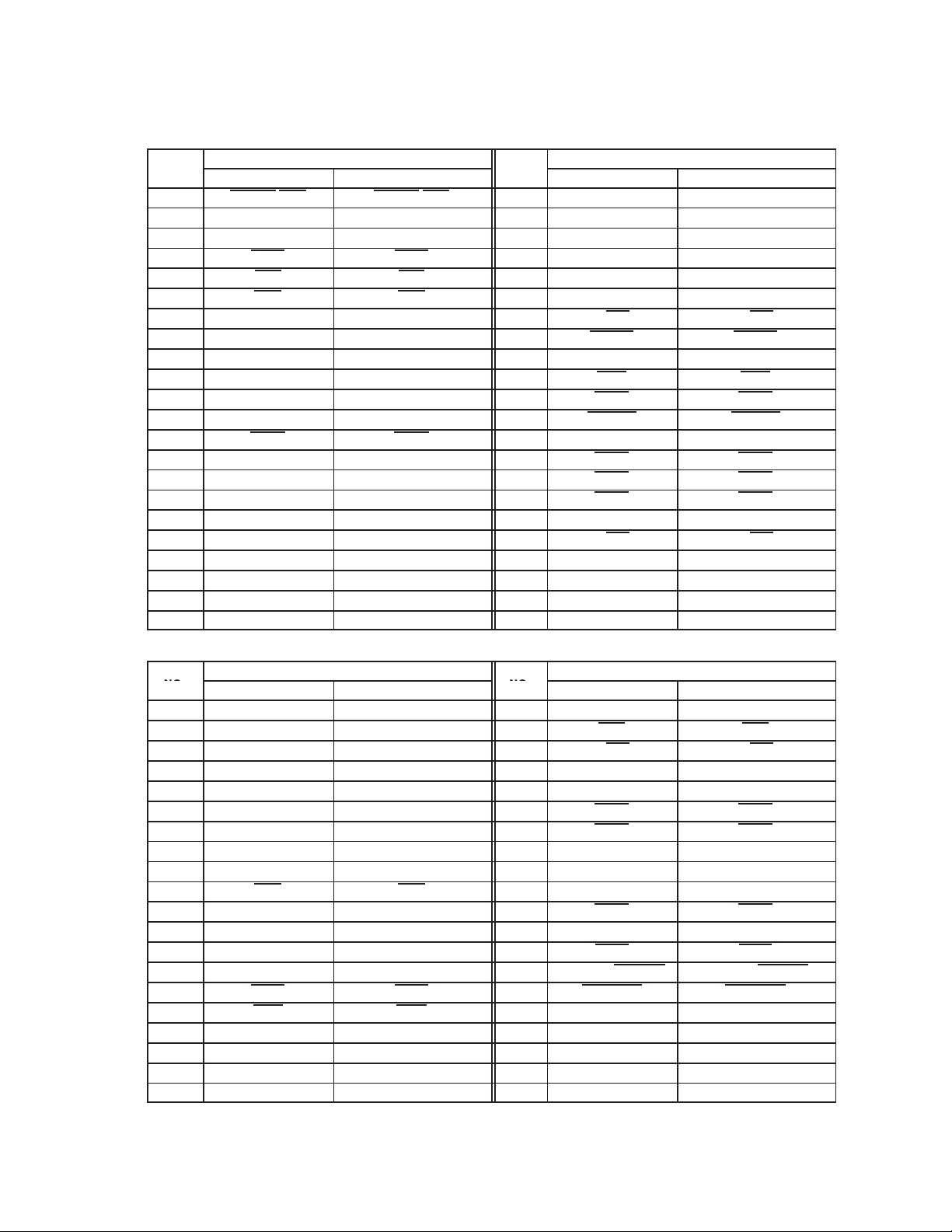
Table 2−1. Signal Names by PDV Terminal Number (Continued)
TERM.
TERM.
TERM.
TERM.
.
.
TERM.
TERM.
SIGNAL NAME
NO.
165 RI_OUT/PME RI_OUT/PME 187 AD21 AD21
166 GND GND 188 AD20 AD20
167 AD25 AD25 189 AD19 AD19
168 PRST PRST 190 AD18 AD18
169 GNT GNT 191 AD17 AD17
170 REQ REQ 192 AD16 AD16
171 AD31 AD31 193 C/BE2 C/BE2
172 AD30 AD30 194 FRAME FRAME
173 AD11 AD11 195 V
174 V
175 AD29 AD29 197 TRDY TRDY
176 AD28 AD28 198 DEVSEL DEVSEL
177 GRST GRST 199 GND GND
178 AD27 AD27 200 STOP STOP
179 AD26 AD26 201 PERR PERR
180 V
181 AD24 AD24 203 PAR PAR
182 PCLK PCLK 204 C/BE1 C/BE1
183 IDSEL IDSEL 205 AD15 AD15
184 AD23 AD23 206 AD14 AD14
185 GND GND 207 AD13 AD13
186 AD22 AD22 208 AD12 AD12
CardBus PC Card 16-Bit PC Card
CC
CCP
V
V
CC
CCP
NO.
196 IRDY IRDY
202 SERR SERR
CardBus PC Card 16-Bit PC Card
CC
SIGNAL NAME
V
CC
Table 2−2. Signal Names by GHK Terminal Number
TERM
NO.
A04 AD12 AD12 B12 AD11 AD11
A05 PAR PAR B13 GNT GNT
A06 GND GND B14 C/BE3 C/BE3
A07 V
A08 AD18 AD18 C05 AD13 AD13
A09 GND GND C06 SERR SERR
A10 V
A11 AD29 AD29 C08 AD16 AD16
A12 V
A13 REQ REQ C10 PCLK PCLK
A14 GND GND C11 GRST GRST
A15 MFUNC5 MFUNC5 C12 AD30 AD30
A16 MFUNC1 MFUNC1 C13 PRST PRST
B05 AD15 AD15 C14 MFUNC6/CLKRUN MFUNC6/CLKRUN
B06 STOP STOP C15 SUSPEND SUSPEND
B07 IRDY IRDY D01 AD10 AD10
B08 AD17 AD17 D19 MFUNC0 MFUNC0
B09 AD22 AD22 E01 GND GND
B10 AD24 AD24 E02 AD7 AD7
B11 AD28 AD28 E03 AD9 AD9
CardBus PC Card 16-Bit PC Card
CC
CCP
CC
SIGNAL NAME
V
V
V
CC
CCP
CC
TERM
NO.
B15 MFUNC4 MFUNC4
C07 TRDY TRDY
C09 AD21 AD21
CardBus PC Card 16-Bit PC Card
SIGNAL NAME
2−5

Table 2−2. Signal Names by GHK Terminal Number (Continued)
.
.
TERM.
TERM.
TERM
NO.
E05 NC NC H05 B_CCD1 B_CD1
E06 AD14 AD14 H06 AD2 AD2
E07 PERR PERR H14 A_CSTSCHG A_BVD1(STSCHG/RI)
E08 FRAME FRAME H15 A_CCLKRUN A_WP(IOIS16)
E09 AD19 AD19 H17 A_CAUDIO A_BVD2(SPKR)
E10 IDSEL IDSEL H18 A_CSERR A_WAIT
E11 AD27 AD27 H19 A_CINT A_READY(IREQ)
E12 AD31 AD31 J01 B_CAD4 B_D12
E13 RI_OUT/PME RI_OUT/PME J02 B_CAD3 B_D5
E14 MFUNC2 MFUNC2 J03 B_CAD6 B_D13
E17 DATA DATA J05 B_CAD5 B_D6
E18 LATCH LATCH J06 B_RSVD B_D14
E19 A_CAD31 A_D10 J14 A_CAD26 A_A0
F01 AD3 AD3 J15 A_CVS1 A_VS1
F02 AD5 AD5 J17 A_CAD25 A_A1
F03 AD6 AD6 J18 A_CAD24 A_A2
F05 AD8 AD8 J19 V
F06 C/BE1 C/BE1 K01 GND GND
F07 DEVSEL DEVSEL K02 B_CAD7 B_D7
F08 C/BE2 C/BE2 K03 B_CAD8 B_D15
F09 AD20 AD20 K05 B_CC/BE0 B_CE1
F10 AD23 AD23 K06 B_CAD9 B_A10
F11 AD26 AD26 K14 A_CC/BE3 A_REG
F12 AD25 AD25 K15 A_CAD23 A_A3
F13 MFUNC3 MFUNC3 K17 A_CREQ A_INPACK
F14 SPKROUT SPKROUT K18 A_CAD22 A_A4
F15 CLOCK CLOCK K19 VR_OUT VR_OUT
F17 A_RSVD A_D2 L01 VR_EN VR_EN
F18 A_CAD29 A_D1 L02 B_CAD10 B_CE2
F19 GND GND L03 B_CAD11 B_OE
G01 V
G02 AD0 AD0 L06 B_CAD12 B_A11
G03 AD1 AD1 L14 A_CAD21 A_A5
G05 AD4 AD4 L15 A_CRST A_RESET
G06 C/BE0 C/BE0 L17 A_CAD20 A_A6
G14 A_CAD28 A_D8 L18 A_CVS2 A_VS2
G15 A_CAD30 A_D9 L19 A_CAD19 A_A25
G17 A_CAD27 A_D0 M01 B_CAD15 B_IOWR
G18 A_CCD2 A_CD2 M02 B_CAD14 B_A9
G19 V
H01 B_CAD1 B_D4 M05 B_RSVD B_A18
H02 B_CAD2 B_D11 M06 B_CC/BE1 B_A8
H03 B_CAD0 B_D3 M14 A_CCLK A_A16
CardBus PC Card 16-Bit PC Card
CC
CC
SIGNAL NAME
V
CC
V
CC
TERM
NO.
L05 B_CAD13 B_IORD
M03 B_CAD16 B_A17
CardBus PC Card 16-Bit PC Card
CC
SIGNAL NAME
V
CC
2−6

Table 2−2. Signal Names by GHK Terminal Number (Continued)
.
.
TERM.
TERM.
TERM
NO.
M15 A_CFRAME A_A23 R14 A_CAD15 A_IOWR
M17 A_CC/BE2 A_A12 R17 A_RSVD A_A18
M18 A_CAD17 A_A24 R18 A_CPERR A_A14
M19 A_CAD18 A_A7 R19 GND GND
N01 V
N02 B_CPAR B_A13 T19 A_CC/BE1 A_A8
N03 B_CBLOCK B_A19 U05 B_CAD18 B_A7
N05 B_CGNT B_WE U06 B_CAD21 B_A5
N06 B_CPERR B_A14 U07 B_CC/BE3 B_REG
N14 A_CBLOCK A_A19 U08 B_CVS1 B_VS1
N15 A_CDEVSEL A_A21 U09 B_CSTSCHG B_BVD1(STSCHG/RI)
N17 A_CTRDY A_A22 U10 B_CAD29 B_D1
N18 A_CIRDY A_A15 U11 A_CCD1 A_CD1
N19 V
P01 GND GND U13 A_CAD7 A_D7
P02 B_CSTOP B_A20 U14 A_CAD10 A_CE2
P03 B_CDEVSEL B_A21 U15 A_CAD14 A_A9
P05 B_CIRDY B_A15 V05 B_CAD20 B_A6
P06 B_CCLK B_A16 V06 B_CAD22 B_A4
P07 B_CVS2 B_VS2 V07 B_CAD24 B_A2
P08 B_CAD23 B_A3 V08 B_CINT B_READY(IREQ)
P09 B_CCD2 B_CD2 V09 B_CAUDIO B_BVD2(SPKR)
P10 B_RSVD B_D2 V10 B_CAD28 B_D8
P11 A_CAD0 A_D3 V11 B_CAD31 B_D10
P12 A_CAD6 A_D13 V12 A_CAD4 A_D12
P13 A_CAD8 A_D15 V13 A_RSVD A_D14
P14 A_CAD12 A_A11 V14 A_CC/BE0 A_CE1
P15 A_CPAR A_A13 V15 A_CAD13 A_IORD
P17 A_CSTOP A_A20 W04 B_CAD17 B_A24
P18 A_CGNT A_WE W05 B_CRST B_RESET
P19 V
R01 V
R02 B_CTRDY B_A22 W08 V
R03 B_CFRAME B_A23 W09 B_CSERR B_WAIT
R06 B_CAD19 B_A25 W10 B_CAD27 B_D0
R07 B_CREQ B_INPACK W11 CLK48 CLK48
R08 B_CAD26 B_A0 W12 A_CAD1 A_D4
R09 B_CCLKRUN B_WP(IOIS16) W13 V
R10 B_CAD30 B_D9 W14 GND GND
R11 A_CAD2 A_D11 W15 A_CAD11 A_OE
R12 A_CAD5 A_D6 W16 A_CAD16 A_A17
R13 A_CAD9 A_A10
CardBus PC Card 16-Bit PC Card
CC
CC
CCA
CCB
SIGNAL NAME
V
V
V
V
CC
CC
CCA
CCB
TERM
NO.
T01 B_CC/BE2 B_A12
U12 A_CAD3 A_D5
W06 GND GND
W07 B_CAD25 B_A1
CardBus PC Card 16-Bit PC Card
CC
CC
SIGNAL NAME
V
V
CC
CC
2−7

Table 2−3. CardBus PC Card Signal Names Sorted Alphabetically
SIGNAL NAME
SIGNAL NAME
SIGNAL NAME
SIGNAL NAME
TERM NO.
PDV GHK
A_CAD0 84 P11 A_CC/BE1 105 T19 AD10 1 D01 B_CAD13 33 L05
A_CAD1 86 W12 A_CC/BE2 120 M17 AD11 173 B12 B_CAD14 35 M02
A_CAD2 85 R11 A_CC/BE3 132 K14 AD12 208 A04 B_CAD15 34 M01
A_CAD3 88 U12 A_CCD1 83 U11 AD13 207 C05 B_CAD16 36 M03
A_CAD4 87 V12 A_CCD2 144 G18 AD14 206 E06 B_CAD17 53 W04
A_CAD5 90 R12 A_CCLK 115 M14 AD15 205 B05 B_CAD18 54 U05
A_CAD6 89 P12 A_CCLKRUN 142 H15 AD16 192 C08 B_CAD19 55 R06
A_CAD7 93 U13 A_CDEVSEL 113 N15 AD17 191 B08 B_CAD20 57 V05
A_CAD8 94 P13 A_CFRAME 119 M15 AD18 190 A08 B_CAD21 59 U06
A_CAD9 97 R13 A_CGNT 112 P18 AD19 189 E09 B_CAD22 60 V06
A_CAD10 98 U14 A_CINT 138 H19 AD20 188 F09 B_CAD23 63 P08
A_CAD11 99 W15 A_CIRDY 117 N18 AD21 187 C09 B_CAD24 65 V07
A_CAD12 100 P14 A_CPAR 107 P15 AD22 186 B09 B_CAD25 66 W07
A_CAD13 101 V15 A_CPERR 109 R18 AD23 184 F10 B_CAD26 67 R08
A_CAD14 103 U15 A_CREQ 130 K17 AD24 181 B10 B_CAD27 76 W10
A_CAD15 102 R14 A_CRST 126 L15 AD25 167 F12 B_CAD28 77 V10
A_CAD16 104 W16 A_CSERR 139 H18 AD26 179 F11 B_CAD29 78 U10
A_CAD17 121 M18 A_CSTOP 111 P17 AD27 178 E11 B_CAD30 79 R10
A_CAD18 122 M19 A_CSTSCHG 141 H14 AD28 176 B11 B_CAD31 82 V11
A_CAD19 123 L19 A_CTRDY 116 N17 AD29 175 A11 B_CAUDIO 72 V09
A_CAD20 125 L17 A_CVS1 137 J15 AD30 172 C12 B_CBLOCK 41 N03
A_CAD21 127 L14 A_CVS2 124 L18 AD31 171 E12 B_CC/BE0 27 K05
A_CAD22 129 K18 A_RSVD 106 R17 B_CAD0 16 H03 B_CC/BE1 37 M06
A_CAD23 131 K15 A_RSVD 92 V13 B_CAD1 18 H01 B_CC/BE2 52 T01
A_CAD24 134 J18 A_RSVD 150 F17 B_CAD2 17 H02 B_CC/BE3 64 U07
A_CAD25 135 J17 AD0 13 G02 B_CAD3 20 J02 B_CCD1 15 H05
A_CAD26 136 J14 AD1 12 G03 B_CAD4 19 J01 B_CCD2 75 P09
A_CAD27 145 G17 AD2 11 H06 B_CAD5 22 J05 B_CCLK 48 P06
A_CAD28 146 G14 AD3 10 F01 B_CAD6 21 J03 B_CCLKRUN 74 R09
A_CAD29 148 F18 AD4 9 G05 B_CAD7 25 K02 B_CDEVSEL 46 P03
A_CAD30 149 G15 AD5 8 F02 B_CAD8 26 K03 B_CFRAME 51 R03
A_CAD31 151 E19 AD6 7 F03 B_CAD9 28 K06 B_CGNT 45 N05
A_CAUDIO 140 H17 AD7 5 E02 B_CAD10 30 L02 B_CINT 69 V08
A_CBLOCK 108 N14 AD8 3 F05 B_CAD11 31 L03 B_CIRDY 50 P05
A_CC/BE0 96 V14 AD9 2 E03 B_CAD12 32 L06 B_CPAR 40 N02
TERM. NO.
PDV GHK
TERM. NO.
PDV GHK
TERM NO.
PDV GHK
2−8

Table 2−3. CardBus PC Card Signal Names Sorted Alphabetically (Continued)
SIGNAL NAME
SIGNAL NAME
TERM NO.
PDV GHK
B_CPERR 42 N06 LATCH 153 E18
B_CREQ 61 R07 MFUNC0 156 D19
B_CRST 58 W05 MFUNC1 157 A16
B_CSERR 71 W09 MFUNC2 159 E14
B_CSTOP 44 P02 MFUNC3 160 F13
B_CSTSCHG 73 U09 MFUNC4 161 B15
B_CTRDY 49 R02 MFUNC5 162 A15
B_CVS1 68 U08 MFUNC6/CLKRUN 163 C14
B_CVS2 56 P07 NC — E05
B_RSVD 23 J06 PAR 203 A05
B_RSVD 38 M05 PCLK 182 C10
B_RSVD 80 P10 PERR 201 E07
C/BE0 4 G06 PRST 168 C13
C/BE1 204 F06 REQ 170 A13
C/BE2 193 F08 RI_OUT/PME 165 E13
C/BE3 164 B14 SERR 202 C06
CLK48 81 W11 SPKROUT 152 F14
CLOCK 154 F15 STOP 200 B06
DATA 155 E17 SUSPEND 158 C15
DEVSEL 198 F07 TRDY 197 C07
FRAME 194 E08 V
GND 6 A06 V
GND 24 A09 V
GND 43 A14 V
GND 62 E01 V
GND 95 K01 V
GND 110 P01 V
GND 147 R19 V
GND 166 W06 V
GND 185 F19 V
GND 199 W14 V
GNT 169 B13 V
GRST 177 C11 VR_EN 29 L01
IDSEL 183 E10 VR_OUT 128 K19
IRDY 196 B07
CC
CC
CC
CC
CC
CC
CC
CC
CC
CCA
CCB
CCP
TERM NO.
PDV GHK
14 A07
39 A12
70 G01
91 G19
118 J19
133 N01
143 N19
174 W08
195 W13
114 P19
47 R01
180 A10
2−9

Table 2−4. 16-Bit PC Card Signal Names Sorted Alphabetically
SIGNAL NAME
SIGNAL NAME
SIGNAL NAME
TERM. NO.
PDV GHK
A_A0 136 J14 A_D10 151 E19 AD24 181 B10
A_A1 135 J17 A_D11 85 R11 AD25 167 F12
A_A2 134 J18 A_D12 87 V12 AD26 179 F11
A_A3 131 K15 A_D13 89 P12 AD27 178 E11
A_A4 129 K18 A_D14 92 V13 AD28 176 B11
A_A5 127 L14 A_D15 94 P13 AD29 175 A11
A_A6 125 L17 A_INPACK 130 K17 AD30 172 C12
A_A7 122 M19 A_IORD 101 V15 AD31 171 E12
A_A8 105 T19 A_IOWR 102 R14 B_A0 67 R08
A_A9 103 U15 A_OE 99 W15 B_A1 66 W07
A_A10 97 R13 A_READY(IREQ) 138 H19 B_A2 65 V07
A_A11 100 P14 A_REG 132 K14 B_A3 63 P08
A_A12 120 M17 A_RESET 126 L15 B_A4 60 V06
A_A13 107 P15 A_VS1 137 J15 B_A5 59 U06
A_A14 109 R18 A_VS2 124 L18 B_A6 57 V05
A_A15 117 N18 A_WAIT 139 H18 B_A7 54 U05
A_A16 115 M14 A_WE 112 P18 B_A8 37 M06
A_A17 104 W16 A_WP(IOIS16) 142 H15 B_A9 35 M02
A_A18 106 R17 AD0 13 G02 B_A10 28 K06
A_A19 108 N14 AD1 12 G03 B_A11 32 L06
A_A20 111 P17 AD2 11 H06 B_A12 52 T01
A_A21 113 N15 AD3 10 F01 B_A13 40 N02
A_A22 116 N17 AD4 9 G05 B_A14 42 N06
A_A23 119 M15 AD5 8 F02 B_A15 50 P05
A_A24 121 M18 AD6 7 F03 B_A16 48 P06
A_A25 123 L19 AD7 5 E02 B_A17 36 M03
A_BVD1(STSCHG/RI) 141 H14 AD8 3 F05 B_A18 38 M05
A_BVD2(SPKR) 140 H17 AD9 2 E03 B_A19 41 N03
A_CD1 83 U11 AD10 1 D01 B_A20 44 P02
A_CD2 144 G18 AD11 173 B12 B_A21 46 P03
A_CE1 96 V14 AD12 208 A04 B_A22 49 R02
A_CE2 98 U14 AD13 207 C05 B_A23 51 R03
A_D0 145 G17 AD14 206 E06 B_A24 53 W04
A_D1 148 F18 AD15 205 B05 B_A25 55 R06
A_D2 150 F17 AD16 192 C08 B_BVD1(STSCHG/RI) 73 U09
A_D3 84 P11 AD17 191 B08 B_BVD2(SPKR) 72 V09
A_D4 86 W12 AD18 190 A08 B_CD1 15 H05
A_D5 88 U12 AD19 189 E09 B_CD2 75 P09
A_D6 90 R12 AD20 188 F09 B_CE1 27 K05
A_D7 93 U13 AD21 187 C09 B_CE2 30 L02
A_D8 146 G14 AD22 186 B09 B_D0 76 W10
A_D9 149 G15 AD23 184 F10 B_D1 78 U10
TERM. NO.
PDV GHK
TERM NO.
PDV GHK
2−10
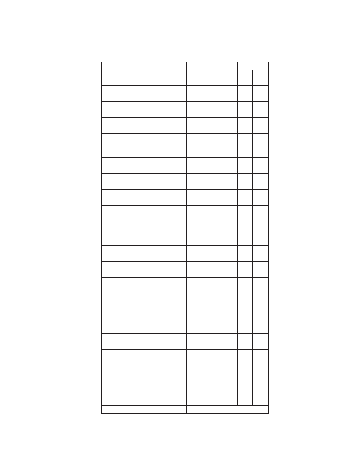
Table 2−4. 16-Bit PC Card Signal Names Sorted Alphabetically (Continued)
SIGNAL NAME
SIGNAL NAME
TERM NO.
PDV GHK
B_D2 80 P10 GND 147 R19
B_D3 16 H03 GND 166 W06
B_D4 18 H01 GND 199 W14
B_D5 20 J02 GNT 169 B13
B_D6 22 J05 GRST 177 C11
B_D7 25 K02 IDSEL 183 E10
B_D8 77 V10 IRDY 196 B07
B_D9 79 R10 LATCH 153 E18
B_D10 82 V11 MFUNC0 156 D19
B_D11 17 H02 MFUNC1 157 A16
B_D12 19 J01 MFUNC2 159 E14
B_D13 21 J03 MFUNC3/IRQSER 160 F13
B_D14 23 J06 MFUNC4 161 B15
B_D15 26 K03 MFUNC5 162 A15
B_INPACK 61 R07 MFUNC6/CLKRUN 163 C14
B_IORD 33 L05 NC — E05
B_IOWR 34 M01 PAR 203 A05
B_OE 31 L03 PCLK 182 C10
B_READY(IREQ) 69 V08 PERR 201 E07
B_REG 64 U07 PRST 168 C13
B_RESET 58 W05 REQ 170 A13
B_VS1 68 U08 RI_OUT/PME 165 E13
B_VS2 56 P07 SERR 202 C06
B_WAIT 71 W09 SPKROUT 152 F14
B_WE 45 N05 STOP 200 B06
B_WP(IOIS16) 74 R09 SUSPEND 158 C15
C/BE0 4 G06 TRDY 197 C07
C/BE1 204 F06 V
C/BE2 193 F08 V
C/BE3 164 B14 V
CLK48 185 W11 V
CLOCK 154 F15 V
DATA 155 E17 V
DEVSEL 198 F07 V
FRAME 194 E08 V
GND 6 A06 V
GND 24 A09 V
GND 43 A14 V
GND 62 E01 V
GND 81 F19 VR_EN 29 L01
GND 95 K01 VR_OUT 128 K19
GND 110 P01
CC
CC
CC
CC
CC
CC
CC
CC
CC
CCA
CCB
CCP
TERM NO.
PDV GHK
14 A07
39 A12
70 G01
91 G19
118 J19
133 N01
143 N19
174 W08
195 W13
114 P19
47 R01
180 A10
2−11
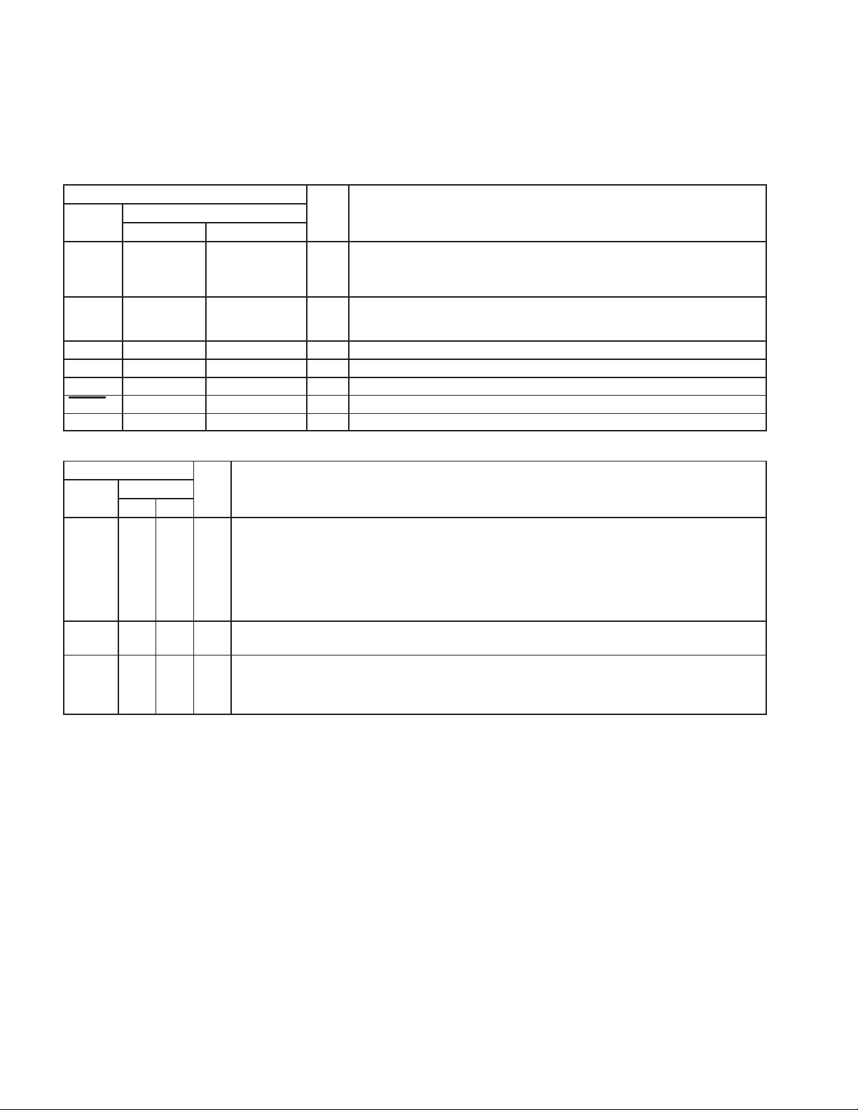
The terminals are grouped in tables by functionality, such as PCI system function and power supply function, for quick
NAME
I/O
DESCRIPTION
NAME
I/O
DESCRIPTION
reference (see Table 2−5 through Table 2−15). The terminal names and numbers are also listed for convenient
reference.
Table 2−5. Power Supply Terminals
TERMINAL
NO.
PDV GHK
GND 6, 24, 43, 62,
V
CC
V
CCA
V
CCB
V
CCP
VR_EN 29 L01 I Internal voltage regulator enable. Active-low
VR_OUT 128 K19 O Internal voltage regulator output (1.8 V) for external bypass capacitor
95, 110, 147,
166, 185, 199
14, 39, 70, 91,
118, 133, 143,
174, 195
114 P19 − PC Card A signaling rail power input; clamped per PC Card specification
47 R01 − PC Card B signaling rail power input; clamped per PC Card specification
180 A10 − PCI signaling clamp rail power input; clamped per PCI specification
A06, A09, A14,
E01, F19, K01,
P01, R19, W06,
W14
A07, A12, G01,
G19, J19, N01,
N19, W08, W13
I/O DESCRIPTION
− Device ground terminals
− 3.3-V power terminals
Table 2−6. PC Card Power Switch Terminals
TERMINAL
NO.
PDV GHK
CLOCK 154 F15 I/O
DATA 155 E17 O
LATCH 153 E18 I/O
I/O DESCRIPTION
Power switch clock. Information on the DATA line is sampled at the rising edge of CLOCK. CLOCK defaults
to an input, but can be changed to a PCI1620 output by using bit 27 (P2CCLK) in the system control register
(PCI offset 80h, see Section 4.31). For use with the TPS222X, the maximum frequency of this signal is limited
to 2 MHz. However, the PCI1620 requires a 16-KHz to 100-KHz frequency range. As an input, this terminal
requires an external 32-kHz clock. If a system design defines this terminal as an output, then this terminal
requires an external pulldown resistor. The frequency of the PCI1620 output CLOCK is derived from the
internal ring oscillator (16 kHz typical).
Power switch data. DATA is used to communicate socket power control information serially to the power
switch.
Power switch latch. LATCH is asserted by the PCI1620 to indicate to the power switch that the data on the
DATA line is valid. The LATCH terminal is also used to indicate the presence of an external EEPROM; when
a pulldown resistor is implemented on this terminal, the MFUNC1 and MFUNC4 terminals provide the serial
EEPROM SDA and SCL interface.
2−12
TERMINAL
NAME
I/O
DESCRIPTION
NO.
PDV GHK
GRST 177 C11 I
PCLK 182 C10 I
PRST
168 C13 I
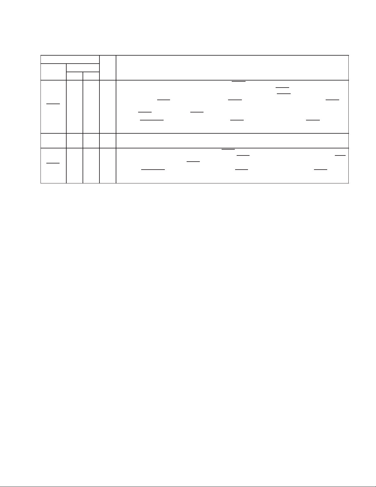
Table 2−7. PCI System Terminals
I/O DESCRIPTION
Global reset. When the global reset is asserted, the GRST signal causes the PCI1620 to place all output
buffers in a high-impedance state and reset all internal registers. When GRST
completely in its default state. For systems that require wake-up from D3, GRST
during initial boot. PRST
that PME context is retained during the transition from D3 to D0. For systems that do not require wake-up
from D3, GRST
When the SUSPEND
registers are not reset, but all outputs are placed in a high-impedance state.
PCI bus clock. PCLK provides timing for all transactions on the PCI bus. All PCI signals are sampled at the
rising edge of PCLK.
PCI reset. When the PCI bus reset is asserted, PRST causes the PCI1620 to reset internal registers and
place all output buffers in a high-impedance state. When PRST
signal only if it is enabled. After PRST is deasserted, the PCI1620 is in a default state.
When the SUSPEND
internal registers are preserved, but all outputs are placed in a high-impedance state.
should be asserted during GRST and for resets subsequent to the initial GRST so
should be tied to PRST.
mode is enabled together with GRST, the device is protected from GRST; the internal
is asserted, the device can generate the PME
mode is enabled together with PRST, the device is protected from PRST and the
is asserted, the device is
normally is asserted only
2−13
TERMINAL
NAME
I/O
DESCRIPTION
NO.
PDV GHK
AD31
AD30
AD29
AD28
AD27
AD26
AD25
AD24
AD23
AD22
AD21
AD20
AD19
AD18
AD17
AD16
AD15
AD14
AD13
AD12
AD11
AD10
AD9
AD8
AD7
AD6
AD5
AD4
AD3
AD2
AD1
AD0
C/BE3
C/BE2
C/BE1
C/BE0
PAR 203 A05 I/O
171
172
175
176
178
179
167
181
184
186
187
188
189
190
191
192
205
206
207
208
173
1
2
3
5
7
8
9
10
11
12
13
164
193
204
4
E12
C12
A11
B11
E11
F11
F12
B10
F10
B09
C09
F09
E09
A08
B08
C08
B05
E06
C05
A04
B12
D01
E03
F05
E02
F03
F02
G05
F01
H06
G03
G02
B14
F08
F06
G06
Table 2−8. PCI Address and Data Terminals
I/O DESCRIPTION
PCI address/data bus. These signals make up the multiplexed PCI address and data bus on the primary
interface. During the address phase of a primary bus PCI cycle, AD31−AD0 contain a 32-bit address or other
I/O
destination information. During the data phase, AD31−AD0 contain data.
PCI bus commands and byte enables. These signals are multiplexed on the same PCI terminals. During
the address phase of a primary bus PCI cycle, C/BE3
phase, this 4-bit bus is used as byte enables. The byte enables determine which byte paths of the full 32-bit
I/O
data bus carry meaningful data. C/BE0
C/BE2
applies to byte 2 (AD23−AD16), and C/BE3 applies to byte 3 (AD31−AD24).
PCI bus parity. In all PCI bus read and write cycles, the PCI1620 calculates even parity across the
AD31−AD0 and C/BE3
indicator with a one-PCLK delay. As a target during PCI cycles, the calculated parity is compared to the parity
indicator of the initiator. A compare error results in the assertion of a parity error (PERR).
−C/BE0 buses. As an initiator during PCI cycles, the PCI1620 outputs this parity
applies to byte 0 (AD7−AD0), C/BE1 applies to byte 1 (AD15−AD8),
−C/BE0 define the bus command. During the data
2−14

Table 2−9. PCI Interface Control Terminals
NAME
I/O
DESCRIPTION
TERMINAL
NO.
PDV GHK
DEVSEL
FRAME
GNT
IDSEL 183 E10 I
IRDY
PERR
REQ
SERR
STOP
TRDY
†
Care must be exercised in selection of the address line that is used for connecting to IDSEL. Check each PCI component to avoid the use of
address lines that it may have reserved, because address lines used can vary from one device to another of the same device type. For example,
one commonly-used chipset uses lines AD11 and AD12, and assignment of IDSEL to either of those lines in an implementation using that chipset
would result in an address conflict.
198 F07 I/O
194 E08 I/O
169 B13 I
196 B07 I/O
201 E07 I/O
170 A13 O PCI bus request. REQ is asserted by the PCI1620 to request access to the PCI bus as an initiator.
202 C06 O
200 B06 I/O
197 C07 I/O
I/O DESCRIPTION
PCI device select. The PCI1620 asserts DEVSEL to claim a PCI cycle as the target device. As a PCI initiator
on the bus, the PCI1620 monitors DEVSEL
occurs, then the PCI1620 terminates the cycle with an initiator abort.
PCI cycle frame. FRAME is driven by the initiator of a bus cycle. FRAME is asserted to indicate that a bus
transaction is beginning, and data transfers continue while this signal is asserted. When FRAME
deasserted, the PCI bus transaction is in the final data phase.
PCI bus grant. GNT is driven by the PCI bus arbiter to grant the PCI1620 access to the PCI bus after the
current data transaction has completed. GNT
bus parking algorithm.
Initialization device select. IDSEL selects the PCI1620 during configuration space accesses. IDSEL can be
connected to one of the upper 24 PCI address lines† on the PCI bus.
PCI initiator ready. IRDY indicates the ability of the PCI bus initiator to complete the current data phase of the
transaction. A data phase is completed on a rising edge of PCLK where both IRDY
Until IRDY
PCI parity error indicator. PERR is driven by a PCI device to indicate that calculated parity does not match
PAR when PERR
PCI system error. SERR is an output that is pulsed from the PCI1620 when enabled through bit 8 of the
command register (PCI offset 04h, see Section 4.4), indicating a system error has occurred. The PCI1620
need not be the target of the PCI cycle to assert this signal. When SERR is enabled in the command register,
this signal also pulses, indicating that an address parity error has occurred on a CardBus interface.
PCI cycle stop signal. STOP is driven by a PCI target to request the initiator to stop the current PCI bus
transaction. STOP
support burst data transfers.
PCI target ready. TRDY indicates the ability of the primary bus target to complete the current data phase of
the transaction. A data phase is completed on a rising edge of PCLK when both IRDY
Until both IRDY
and TRDY are both sampled asserted, wait states are inserted.
is enabled through bit 6 of the command register (PCI offset 04h, see Section 4.4).
is used for target disconnects and is commonly asserted by target devices that do not
and TRDY are asserted, wait states are inserted.
until a target responds. If no target responds before timeout
may or may not follow a PCI bus request, depending on the PCI
and TRDY are asserted.
and TRDY are asserted.
is
2−15

Table 2−10. Multifunction and Miscellaneous Terminals
NAME
I/O
DESCRIPTION
TERMINAL
NO.
PDV GHK
CLK48 81 W11 I 48-MHz clock input. This clock is used as a clock source for internal microcontroller.
MFUNC0 156 D19 I/O
MFUNC1 157 A16 I/O
MFUNC2 159 E14 I/O
MFUNC3/
IRQSER
MFUNC4 161 B15 I/O
MFUNC5 162 A15 I/O
MFUNC6/
CLKRUN
RI_OUT/PME 165 E13 O
SPKROUT
SUSPEND 158 C15 I
160 F13 I/O
163 C14 I/O
152 F14 O
I/O DESCRIPTION
Multifunction terminal 0. MFUNC0 can be configured as parallel PCI interrupt INTA, GPI0, GPO0, socket
activity LED output, ZV switching outputs, CardBus audio PWM, GPE
Section 4.38, Multifunction Routing Status Register, for configuration details.
Multifunction terminal 1. MFUNC1 can be configured as parallel PCI interrupt INTB, GPI1, GPO1, socket
activity LED output, ZV switching outputs, CardBus audio PWM, GPE
Section 4.38, Multifunction Routing Status Register, for configuration details.
Serial data (SDA). When LATCH is detected low during GRST , the MFUNC1 terminal provides the SDA
signaling for the serial bus interface. The two-terminal serial interface loads the subsystem identification
and other register defaults from an EEPROM after a PCI reset. See Section 3.4.4, Loading the
Subsystem Identification (EEPROM Interface), for details on other serial bus applications.
Multifunction terminal 2. MFUNC2 can be configured as GPI2, GPO2, socket activity LED output, ZV
switching outputs, CardBus audio PWM, GPE
Multifunction Routing Status Register , for configuration details.
Multifunction terminal 3. MFUNC3 can be configured as a parallel IRQ or the serialized interrupt signal
IRQSER. See Section 4.38, Multifunction Routing Status Register, for configuration details.
Multifunction terminal 4. MFUNC4 can be configured as PCI LOCK, GPI3, GPO3, socket activity LED
output, ZV switching outputs, CardBus audio PWM, GPE
Multifunction Routing Status Register , for configuration details.
Serial clock (SCL). When LATCH is detected low during GRST , the MFUNC4 terminal provides the SCL
signaling for the serial bus interface. The two-terminal serial interface loads the subsystem identification
and other register defaults from an EEPROM after a PCI reset. See Section 3.4.4, Loading the
Subsystem Identification (EEPROM Interface), for details on other serial bus applications.
Multifunction terminal 5. MFUNC5 can be configured as GPI4, GPO4, socket activity LED output, ZV
switching outputs, CardBus audio PWM, GPE
Status Register, for configuration details.
Multifunction terminal 6. MFUNC6 can be configured as a PCI CLKRUN or a parallel IRQ. See
Section 4.38, Multifunction Routing Status Register, for configuration details.
Ring indicate out and power-management event output. Terminal provides an output for ring-indicate
or PME
signals.
Speaker output. SPKROUT is the output to the host system that can carry SPKR or CAUDIO through
the PCI1620 from the PC Card interface. SPKROUT is driven as the exclusive-OR combination of card
SPKR//CAUDIO inputs.
Suspend. SUSPEND protects the internal registers from clearing when the GRST or PRST signal is
asserted. See Section 3.7.5, Suspend Mode, for details.
, RI_OUT, or a parallel IRQ. See Section 4.38,
, RI_OUT, or a parallel IRQ. See Section 4.38,
, or a parallel IRQ. See Section 4.38, Multifunction Routing
, or a parallel IRQ. See
, or a parallel IRQ. See
2−16

Table 2−11. CardBus PC Card Interface System Terminals (Slots A and B)
I/O
DESCRIPTION
NAME
TERMINAL
NUMBER
†
NAME
CCLK 115 M14 48 P06 O
CCLKRUN
CRST
†
Terminal name for slot A is preceded with A_. For example, the full name for terminals 115 and M14 are A_CCLK.
‡
Terminal name for slot B is preceded with B_. For example, the full name for terminals 48 and P06 are B_CCLK.
SLOT A
PDV GHK PDV GHK
142 H15 74 R09 I/O
126 L15 58 W05 O
SLOT B
‡
CardBus clock. CCLK provides synchronous timing for all transactions on the
CardBus interface. All signals except CRST
, CCD1, CVS2, and CVS1 are sampled on the rising edge of CCLK, and all
CCD2
timing parameters are defined with the rising edge of this signal. CCLK operates at
the PCI bus clock frequency, but it can be stopped in the low state or slowed down
for power savings.
CardBus clock run. CCLKRUN is used by a CardBus PC Card to request an increase
in the CCLK frequency, and by the PCI1620 to indicate that the CCLK frequency is
going to be decreased.
CardBus reset. CRST brings CardBus PC Card-specific registers, sequencers, and
signals to a known state. When CRST
placed in a high-impedance state, and the PCI1620 drives these signals to a valid
logic level. Assertion can be asynchronous to CCLK, but deassertion must be
synchronous to CCLK.
, CCLKRUN, CINT, CSTSCHG, CAUDIO,
is asserted, all CardBus PC Card signals are
2−17

Table 2−12. CardBus PC Card Address and Data Terminals (Slots A and B)
I/O
DESCRIPTION
NAME
TERMINAL
NUMBER
†
NAME
CAD31
CAD30
CAD29
CAD28
CAD27
CAD26
CAD25
CAD24
CAD23
CAD22
CAD21
CAD20
CAD19
CAD18
CAD17
CAD16
CAD15
CAD14
CAD13
CAD12
CAD11
CAD10
CAD9
CAD8
CAD7
CAD6
CAD5
CAD4
CAD3
CAD2
CAD1
CAD0
CC/BE3
CC/BE2
CC/BE1
CC/BE0
CPAR 107 P15 40 N02 I/O
†
Terminal name for slot A is preceded with A_. For example, the full name for terminals 107 and P15 are A_CPAR.
‡
Terminal name for slot B is preceded with B_. For example, the full name for terminals 40 and N02 are B_CPAR.
SLOT A
PDV GHK PDV GHK
151
149
148
146
145
136
135
134
131
129
127
125
123
122
121
104
102
103
101
100
99
98
97
94
93
89
90
87
88
85
86
84
132
120
105
96
E19
G15
F18
G14
G17
J14
J17
J18
K15
K18
L14
L17
L19
M19
M18
W16
R14
U15
V15
P14
W15
U14
R13
P13
U13
P12
R12
V12
U12
R11
W12
P11
K14
M17
T19
V14
82
79
78
77
76
67
66
65
63
60
59
57
55
54
53
36
34
35
33
32
31
30
28
26
25
21
22
19
20
17
18
16
64
52
37
27
SLOT B
‡
V11
R10
U10
V10
W10
R08
W07
V07
P08
V06
U06
V05
R06
U05
W04
M03
M01
M02
L05
L06
L03
L02
K06
K03
K02
J03
J05
J01
J02
H02
H01
H03
U07
T01
M06
K05
CardBus address and data. These signals make up the multiplexed CardBus address
and data bus on the CardBus interface. During the address phase of a CardBus cycle,
I/O
CAD31−CAD0 contain a 32-bit address. During the data phase of a CardBus cycle,
CAD31−CAD0 contain data. CAD31 is the most significant bit.
CardBus bus commands and byte enables. CC/BE3−CC/BE0 are multiplexed on the
same CardBus terminals. During the address phase of a CardBus cycle,
CC/BE3−CC/BE0 define the bus command. During the data phase, this 4-bit bus is used
as byte enables. The byte enables determine which byte paths of the full 32-bit data bus
I/O
carry meaningful data. CC/BE0
byte 1 (CAD15−CAD8), CC/BE2
to byte 3 (CAD31−CAD24).
CardBus parity . In all CardBus read and write cycles, the PCI1620 calculates even parity
across the CADx and CC/BEx
outputs CPAR with a one-CCLK delay. As a target during CardBus cycles, the PCI1620
compares its calculated parity to the parity indicator of the initiator; a compare error
results in a parity error assertion.
applies to byte 0 (CAD7−CAD0), CC/BE1 applies to
applies to byte 2 (CAD23−CAD8), and CC/BE3 applies
buses. As an initiator during CardBus cycles, the PCI1620
2−18

Table 2−13. CardBus PC Card Terminals (Slots A and B)
I/O
DESCRIPTION
NAME
TERMINAL
NUMBER
†
NAME
CAUDIO 140 H17 72 V09 I
CBLOCK
CCD1
CCD2
CDEVSEL
CFRAME
CGNT
SLOT A
PDV GHK PDV GHK
108 N14 41 N03 I/O
83
U11
144
G181575
113 N15 46 P03 I/O
119 M15 51 R03 I/O
112 P18 45 N05 O
SLOT B
‡
H05
P09
CardBus audio. CAUDIO is a digital input signal from a PC Card to the system speaker.
The PCI1620 supports the binary audio mode and outputs a binary signal from the card to
SPKROUT.
CardBus lock. CBLOCK is used to gain exclusive access to a target.
The card-detect terminals and the voltage-sense terminals are used together to determine
the insertion event and type of PC Card inserted (16-bit, CardBus, or UltraMedia). The
I
PCI1620 implements changes in the interrogation logic that handles this function. See
Section 3.5.1, Card Detedtion in an UltraMedia System, for more information.
CardBus device select. The PCI1620 asserts CDEVSEL to claim a CardBus cycle as the
target device. As a CardBus initiator on the bus, the PCI1620 monitors CDEVSEL
target responds. If no target responds before timeout occurs, then the PCI1620 terminates
the cycle with an initiator abort.
CardBus cycle frame. CFRAME is driven by the initiator of a CardBus bus cycle. CFRAME
is asserted to indicate that a bus transaction is beginning, and data transfers continue while
this signal is asserted. When CFRAME
the final data phase.
CardBus bus grant. CGNT is driven by the PCI1620 to grant a CardBus PC Card access
to the CardBus bus after the current data transaction has been completed.
is deasserted, the CardBus bus transaction is in
until a
CINT
CIRDY
CPERR
CREQ
CSERR
CSTOP
CSTSCHG
CTRDY
CVS1
CVS2
138 H19 69 V08 I
117 N18 50 P05 I/O
109 R18 42 N06 I/O
130 K17 61 R07 I
139 H18 71 W09 I
111 P17 44 P02 I/O
141 H14 73 U09 I
116 N17 49 R02 I/O
137
124
J15
L186856
U08
P07
I/O
CardBus interrupt. CINT is asserted low by a CardBus PC Card to request interrupt
servicing from the host.
CardBus initiator ready . CIRDY indicates the ability of the CardBus initiator to complete t he
current data phase of the transaction. A data phase is completed on a rising edge of CCLK
when both CIRDY and CTRDY are asserted. Until CIRDY and CTRDY are both sampled
asserted, wait states are inserted.
CardBus parity error. CPERR reports parity errors during CardBus transactions, except
during special cycles. It is driven low by a target two clocks following the data cycle when
a parity error is detected.
CardBus request. CREQ indicates to the arbiter that the CardBus PC Card desires use of
the CardBus bus as an initiator.
CardBus system error. CSERR reports address parity errors and other system errors that
could lead to catastrophic results. CSERR
deasserted by a weak pullup, and deassertion may take several CCLK periods. The
PCI1620 can report CSERR to the system by assertion of SERR on the PCI interface.
CardBus stop. CSTOP is driven by a CardBus target to request the initiator to stop the
current CardBus transaction. CSTOP
asserted by target devices that do not support burst data transfers.
CardBus status change. CSTSCHG alerts the system to a change in the card status, and
is used as a wake-up mechanism.
CardBus target ready. CTRDY indicates the ability of the CardBus target to complete the
current data phase of the transaction. A data phase is completed on a rising edge of CCLK,
when both CIRDY and CTRDY are asserted; until this time, wait states are inserted.
The card-detect terminals and the voltage-sense terminals are used together to determine
the insertion event and type of PC Card inserted (16-bit, CardBus, or UltraMedia). The
PCI1620 implements changes in the interrogation logic that handles this function.
is driven by the card synchronous to CCLK, but
is used for target disconnects, and is commonly
†
Terminal name for slot A is preceded with A_. For example, the full name for terminals 140 and H17 are A_CAUDIO.
‡
Terminal name for slot B is preceded with B_. For example, the full name for terminals 72 and V09 are B_CAUDIO.
2−19

Table 2−14. 16-Bit PC Card Address and Data Terminals (Slots A and B)
I/O
DESCRIPTION
NAME
TERMINAL
NUMBER
†
NAME
A25
A24
A23
A22
A21
A20
A19
A18
A17
A16
A15
A14
A13
A12
A11
A10
A9
A8
A7
A6
A5
A4
A3
A2
A1
A0
D15
D14
D13
D12
D11
D10
D9
D8
D7
D6
D5
D4
D3
D2
D1
D0
†
Terminal name for slot A is preceded with A_. For example, the full name for terminals 123 and L19 are A_A25.
‡
Terminal name for slot B is preceded with B_. For example, the full name for terminals 55 and R06 are B_A25.
SLOT A
PDV
123
121
119
116
113
111
108
106
104
115
117
109
107
120
100
97
103
105
122
125
127
129
131
134
135
136
94
92
89
87
85
151
149
146
93
90
88
86
84
150
148
145
GHK
L19
M18
M15
N17
N15
P17
N14
R17
W16
M14
N18
R18
P15
M17
P14
R13
U15
T19
M19
L17
L14
K18
K15
J18
J17
J14
P13
V13
P12
V12
R11
E19
G15
G14
U13
R12
U12
W12
P11
F17
F18
G17
PDV
55
53
51
49
46
44
41
38
36
48
50
42
40
52
32
28
35
37
54
57
59
60
63
65
66
67
26
23
21
19
17
82
79
77
25
22
20
18
16
80
78
76
SLOT B
‡
GHK
R06
W04
R03
R02
P03
P02
N03
M05
M03
P06
P05
N06
N02
T01
L06
K06
M02
M06
U05
V05
U06
V06
P08
V07
W07
R08
K03
J06
J03
J01
H02
V11
R10
V10
K02
J05
J02
H01
H03
P10
U10
W10
O PC Card address. 16-bit PC Card address lines. A25 is the most significant bit.
I/O PC Card data. 16-bit PC Card data lines. D15 is the most significant bit.
2−20

Table 2−15. 16-Bit PC Card Interface Control Terminals (Slots A and B)
I/O
DESCRIPTION
NAME
TERMINAL
NUMBER
†
NAME
BVD1
(STSCHG
†
Terminal name for slot A is preceded with A_. For example, the full name for terminals 141 and H14 are A_BVD1(STSCHG
‡
Terminal name for slot B is preceded with B_. For example, the full name for terminals 73 and U09 are B_BVD1(STSCHG
/RI)
BVD2
(SPKR
)
CE1
CE2
INPACK 130 K17 61 R07 I
IORD
IOWR
OE 99 W15 31 L03 O
READY
(IREQ
)
REG
SLOT A
PDV GHK PDV GHK
141 H14 73 U09 I
140 H17 72 V09 I
9698V14
U142730
101 V15 33 L05 O
102 R14 34 M01 O
138 H19 69 V08 I
132 K14 64 U07 O
SLOT B
‡
K05
L02
Battery voltage detect 1. BVD1 is generated by 16-bit memory PC Cards that
include batteries. BVD1 is used with BVD2 as an indication of the condition of the
batteries on a memory PC Card. Both BVD1 and BVD2 are high when the battery
is good. When BVD2 is low and BVD1 is high, the battery is weak and should be
replaced. When BVD1 is low, the battery is no longer serviceable and the data in
the memory PC Card is lost. See Section 5.6, ExCA Card Status-Change Interrupt
Configuration Register, for enable bits. See Section 5.5, ExCA Card
Status-Change Register, and Section 5.2, ExCA Interface Status Register, for the
status bits for this signal.
Status change. STSCHG
write-protect, or battery voltage detect condition of a 16-bit I/O PC Card.
Ring indicate. RI is used by 16-bit modem cards to indicate a ring detection.
Battery voltage detect 2. BVD2 is generated by 16-bit memory PC Cards that
include batteries. BVD2 is used with BVD1 as an indication of the condition of the
batteries on a memory PC Card. Both BVD1 and BVD2 are high when the battery
is good. When BVD2 is low and BVD1 is high, the battery is weak and should be
replaced. When BVD1 is low, the battery is no longer serviceable and the data in
the memory PC Card is lost. See Section 5.6, ExCA Card Status-Change Interrupt
Configuration Register, for enable bits. See Section 5.5, ExCA Card
Status-Change Register, and Section 5.2, ExCA Interface Status Register, for the
status bits for this signal.
Speaker. SPKR
socket have been configured for the 16-bit I/O interface. The audio signals from
cards A and B are combined by the PCI1620 and are output on SPKROUT.
Card enable 1 and card enable 2. CE1 and CE2 enable even- and odd-numbered
address bytes. CE1
O
odd-numbered address bytes.
Input acknowledge. INPACK is asserted by the PC Card when it can respond to an
I/O read cycle at the current address.
I/O read. IORD is asserted by the PCI1620 to enable 16-bit I/O PC Card data output
during host I/O read cycles.
I/O write. IOWR is driven low by the PCI1620 to strobe write data into 16-bit I/O PC
Cards during host I/O write cycles.
Output enable. OE is driven low by the PCI1620 to enable 16-bit memory PC Card
data output during host memory read cycles.
Ready. The ready function is provided by READY when the 16-bit PC Card and the
host socket are configured for the memory-only interface. READY is driven low by
the 16-bit memory PC Cards to indicate that the memory card circuits are busy
processing a previous write command. READY is driven high when the 16-bit
memory PC Card is ready to accept a new data transfer command.
Interrupt request. IREQ
that a device on the 16-bit I/O PC Card requires service by the host software. IREQ
is high (deasserted) when no interrupt is requested.
Attribute memory select. REG remains high for all common memory accesses.
When REG
to the I/O space (IORD
section of card memory and is generally used to record card capacity and other
configuration and attribute information.
is an optional binary audio signal available only when the card and
is asserted, access is limited to attribute memory (OE or WE active) and
is used to alert the system to a change in the READY,
enables even-numbered address bytes, and CE2 enables
is asserted by a 16-bit I/O PC Card to indicate to the host
or IOWR active). Attribute memory is a separately accessed
/RI).
/RI).
2−21

Table 2−15. 16-Bit PC Card Interface Control Terminals (Slots A and B) (Continued)
I/O
DESCRIPTION
NAME
TERMINAL
NUMBER
†
NAME
RESET 126 L15 58 W05 O PC Card reset. RESET forces a hard reset to a 16-bit PC Card.
WAIT
WE 112 P18 45 N05 O
WP
(IOIS16
†
Terminal name for slot A is preceded with A_. For example, the full name for terminals 99 and W15 are A_OE
‡
Terminal name for slot B is preceded with B_. For example, the full name for terminals 31 and L03 are B_OE
SLOT A
PDV GHK PDV GHK
139 H18 71 W09 I
142 H15 74 R09 I
)
SLOT B
‡
Bus cycle wait. WAIT is driven by a 16-bit PC Card to extend the completion of the memory
or I/O cycle in progress.
Write enable. WE is used to strobe memory write data into 16-bit memory PC Cards. WE
is also used for memory PC Cards that employ programmable memory technologies.
Write protect. WP applies to 16-bit memory PC Cards. WP reflects the status of the
write-protect switch on 16-bit memory PC Cards. For 16-bit I/O cards, WP is used for the
16-bit port (IOIS16) function.
I/O is 16 bits. IOIS16
when the address on the bus corresponds to an address to which the 16-bit PC Card
responds, and the I/O port that is addressed is capable of 16-bit accesses.
applies to 16-bit I/O PC Cards. IOIS16 is asserted by the 16-bit PC Card
.
.
2−22

UltraMedia defines additional functionality for the CardBus/PC Card terminals. Table 2−16 gives the signal names
CARD
CARD
16-Bit PC Card
CardBus
and mapping of this additional functionality to the PCI1620 CardBus/PC Card terminals, with reference to the 68-pin
card socket. Table 2−17 provides the signal descriptions.
Table 2−16. UltraMedia Mapping to the PCMCIA 68-Terminal Connector
UltraMedia
PIN
1 GND GND GND GND GND GND
2 D3 CAD0 RSVD RSVD RSVD RSVD
3 D4 CAD1 RSVD RSVD RSVD RSVD
4 D5 CAD3 SM_D3 RSVD MS_BS RSVD
5 D6 CAD5 SM_D2 RSVD MS_SDIO RSVD
6 D7 CAD7 SM_D1 RSVD MS_RFU5 RSVD
7 CE1 CC/BE0 SM_D0 RSVD MS_RFU7 RSVD
8 A10 CAD9 SM_WP RSVD RSVD RSVD
9 OE CAD11 SM_R/B RSVD RSVD RSVD
10 A11 CAD12 RSVD RSVD RSVD RSVD
11 A9 CAD14 RSVD RSVD RSVD RSVD
12 A8 CC/BE1 SM_RE RSVD RSVD RSVD
13 A13 CPAR SM_WE RSVD RSVD RSVD
14 A14 CPERR RSVD SD_DATA1/IRQ RSVD RSVD
15 WE CGNT SM_ALE RSVD RSVD SC_RFU
16 READY/IREQ CINT RSVD SD_CD/DATA3 RSVD RSVD
17 V
18 VPP/V
19 A16 CCLK RSVD SD_CLK MS_SCLK SC_CLK
20 A15 CIRDY MC_WP MC_WP RSVD RSVD
21 A12 CC/BE2 SM_CLE RSVD RSVD SC_RST
22 A7 CAD18 RSVD RSVD RSVD SC_GPIO0
23 A6 CAD20 RSVD RSVD RSVD SC_GPIO1
24 A5 CAD21 RSVD RSVD RSVD SC_GPIO2
25 A4 CAD22 RSVD RSVD RSVD SC_GPIO3
26 A3 CAD23 RSVD RSVD RSVD SC_GPIO4
27 A2 CAD24 RSVD RSVD RSVD SC_GPIO5
28 A1 CAD25 RSVD RSVD RSVD SC_GPIO06
29 A0 CAD26 RSVD RSVD RSVD SC_GPIO7
30 D0 CAD27 RSVD RSVD RSVD RSVD
31 D1 CAD29 RSVD RSVD RSVD RSVD
32 D2 RFU RSVD RSVD RSVD RSVD
33 WP(IOIS16) CCLKRUN RSVD RSVD RSVD RSVD
34 GND GND GND GND GND GND
35 GND GND GND GND GND GND
36 CD1 CCD1 CCD1 CCD1 CCD1 CCD1
37 D11 CAD2 SM_D4 RSVD RSVD RSVD
38 D12 CAD4 SM_D5 RSVD RSVD RSVD
39 D13 CAD6 SM_D6 RSVD RSVD RSVD
40 D14 RFU SM_D7 RSVD RSVD RSVD
CC
CORE
V
VPP/V
CC
CORE
SmartMedia MMC/SD Memory Stick Smart Card
V
VPP/V
CC
CORE
V
VPP/V
CC
CORE
V
VPP/V
CC
CORE
V
VPP/V
CC
CORE
2−23

Table 2−16. UltraMedia Mapping to the PCMCIA 68-Terminal Connector (Continued)
TERM.
16-Bit PC Card
CardBus
UltraMedia
SmartMedia MMC/SD Memory Stick Smart Card
41 D15 CAD8 SM_LVD RSVD RSVD RSVD
42 CE2 CAD10 RSVD RSVD RSVD RSVD
43 VS1 CVS1 CVS1 CVS1 CVS1 CVS1
44 IORD/RFU CAD13 RSVD RSVD RSVD RSVD
45 IOWR/RFU CAD15 RSVD RSVD RSVD RSVD
46 A17 CAD16 RSVD RSVD RSVD RSVD
47 A18 RFU SQRY1 SQRY1 SQRY1 SQRY1
48 A19 CBLOCK RSVD SD_DATA0 RSVD RSVD
49 A20 CSTOP RSVD SD_CMD RSVD RSVD
50 A21 CDEVSEL RSVD SD_DATA2 RSVD RSVD
51 V
52 VPP/V
53 A22 CTRDY MC_CD MC_CD MC_CD MC_CD
54 A23 CFRAME RSVD RSVD RSVD SC_FCB
55 A24 CAD17 SM_CE RSVD RSVD SC_I/O
56 A25 CAD19 SQRYDR SQRYDR SQRYDR SQRYDR
57 VS2 CVS2 CVS2 CVS2 CVS2 CVS2
58 RESET CRST SQRY2 SQRY2 SQRY2 SQRY2
59 WAIT CSERR SQRY3 SQRY3 SQRY3 SQRY3
60 INPACK/RFU CREQ SQRY4 SQRY4 SQRY4 SQRY4
61 REG CC/BE3 SQRY5 SQRY5 SQRY5 SQRY5
62 BVD2(SPKR) CAUDIO SQRY6 SQRY6 SQRY6 SQRY6
63 BVD1(STSCHG/RI) CSTSCHG SQRY7 SQRY7 SQRY7 SQRY7
64 D8 CAD28 SQRY8 SQRY8 SQRY8 SQRY8
65 D9 CAD30 SQRY9 SQRY9 SQRY9 SQRY9
66 D10 CAD31 SQRY10 SQRY10 SQRY10 SQRY10
67 CD2 CCD2 CCD2 CCD2 CCD2 CCD2
68 GND GND GND GND GND GND
CC
CORE
V
VPP/V
CC
CORE
V
VPP/V
CC
CORE
V
VPP/V
CC
CORE
V
VPP/V
CC
CORE
V
VPP/V
CC
CORE
2−24

Table 2−17. UltraMedia Terminals (Slots A and B)
I/O
DESCRIPTION
NAME
Smart Card general-purpose I/O terminals. These signals can be controlled by firmware
I/O
Smart Card general-purpose I/O terminals. These signals can be controlled by firmware
.
and are used as control signals for an external Smart Card interface chip or level shifter.
TERMINAL
NO.
NAME
MC_CD 116 N17 49 R02 I
MC_WP 117 N18 50 P05 I
MS_BS 88 U12 20 J02 O Memory Stick bus state. This signal provides Memory Stick bus state information.
MS_RFU5 93 U13 25 K02 I
MS_RFU7 96 V14 27 K05 I
MS_SCLK 115 M14 48 P06 O Memory Stick clock. This output provides the MS clock, which operates at 16 MHz.
MS_SDIO 90 R12 22 J05 I/O Memory Stick serial data I/O. This signal provides Memory Stick data input/output.
SC_CLK 115 M14 48 P06 O
SC_FCB 119 M15 51 R03 I
SC_GPIO0 122 M19 54 U05
SC_GPIO1 125 L17 57 V05
SC_GPIO2 127 L14 59 U06
SC_GPIO3 129 K18 60 V06
SC_GPIO4 131 K15 63 P08
SC_GPIO5 134 J18 65 V07
SC_GPIO6 135 J17 66 W07
SC_GPIO7 136 J14 67 R08
SC_IO 121 M18 53 W04 I/O
SC_RFU 112 P18 45 N05 I
SC_RST 120 M17 52 T01 O
SD_CD/
DATA3
SD_CLK 115 M14 48 P06 O SD flash clock. This output provides the MMC/SD clock, which operates at 16 MHz.
SD_CMD 111 P17 44 P02 I/O SD flash command. This signal provides the SD command per the SD specification.
SD_DATA0 108 N14 41 N03 I/O SD flash data 0. This signal provides the MMC_SD data path per the SD specification.
SD_DATA1 109 R18 42 N06 I/O SD flash data 1. This signal provides the SD data path per the SD specification.
SD_DATA2 113 N15 46 P03 I/O SD flash data 2. This signal provides the SD data path and CD per the SD specification.
SM_ALE 112 P18 45 N05 O
SM_CE 121 M18 53 W04 O
SM_CLE 120 M17 52 T01 O
SLOT A SLOT B
PDV GHK PDV GHK
138 H19 69 V08 I/O
Media Card detect. This input is asserted when an UltraMedia adapter and its associated
media are inserted. For all other UltraMedia cards, the UltraMedia socket is not powered
until this signal is low.
UltraMedia write protect data. This signal indicates that the media inserted in the socket is
write protected.
Memory Stick reserved. This terminal is in a high-impedance state when an UltraMedia
Memory Stick adapter has been inserted.
Memory Stick reserved. This terminal is in a high-impedance state when an UltraMedia
Memory Stick adapter has been inserted.
Smart Card clock. The PCI1620 drives a 3-MHz clock to the Smart Card interface when
enabled.
Smart Card function code. The PCI1620 does not support synchronous Smart Cards as
specified in ISO/IEC 7816-10, and this terminal is in a high-impedance state when an
UltraMedia Smart Card adapter has been inserted.
and are used as control signals for an external Smart Card interface chip or level shifter
Smart Card input/output. This terminal is the input/output terminal for the character
exchange between the PCI1620 and the Smart Cards.
Smart Card reserved. This terminal is in a high-impedance state when an UltraMedia
Smart Card adapter has been inserted.
Smart Card reset. This signal starts and stops the Smart Card reset sequence. The
PCI1620 asserts this reset when requested by the host.
SD flash card detect/data 3. This signal provides the SD data path per the SD
specification.
SmartMedia address latch enable. This signal functions as specified in the SmartMedia
specification, and is used to latch addresses passed over SM_D7−SM_D0.
SmartMedia card enable. This signal functions as specified in the SmartMedia
specification, and is used to enable the media for a pending transaction.
SmartMedia command latch enable. This signal functions as specified in the SmartMedia
specification, and is used to latch commands passed over SM_D7−SM_D0.
2−25

Table 2−17. UltraMedia Terminals (Slots A & B) (Continued)
I/O
DESCRIPTION
NAME
SmartMedia data terminals. These signals pass data to and from the SmartMedia, and
SmartMedia data terminals. These signals pass data to and from the SmartMedia, and
function as specified in the SmartMedia specification.
Query return terminals. These terminals are connected to the query driver terminal or to
Query return terminals. These terminals are connected to the query driver terminal or to
ground, to indicate the functionality of the UltraMedia card.
TERMINAL
NO.
NAME
SM_D0 96 V14 27 K05
SM_D1 93 U13 25 K02
SM_D2 90 R12 22 J05
SM_D3 88 U12 20 J02
SM_D4 85 R11 17 H02
SM_D5 87 V12 19 J01
SM_D6 89 P12 21 J03
SM_D7 92 V13 23 J06
SM_LVD 94 P13 26 K03 I
SM_R/B 99 W15 31 L03 I
SM_RE 105 T19 37 M06 O
SM_WE 107 P15 40 N02 O
SM_WP 97 R13 28 K06 O
SQRY1 106 R17 38 M05
SQRY2 126 L15 58 W05
SQRY3 139 H18 71 W09
SQRY4 130 K17 61 R07
SQRY5 132 K14 64 U07
SQRY6 140 H17 72 V09
SQRY7 141 H14 73 U09
SQRY8 146 G14 77 V10
SQRY9 149 G15 79 R10
SQRY10 151 E19 82 V11
SQRYDRV 123 L19 55 R06 O
SLOT A SLOT B
PDV GHK PDV GHK
I/O
function as specified in the SmartMedia specification.
SmartMedia low-voltage detect. This signal, when asserted, indicates that a 3.3V
SmartMedia card is inserted in the socket. When deasserted (low), the SmartMedia card
in the socket is a 5-V card.
SmartMedia ready/busy. This signal functions as specified in the SmartMedia
specification, and is used to pace data transfers to the card.
SmartMedia read enable. This signal functions as specified in the SmartMedia
specification, and is used to latch a read transfer from the card.
SmartMedia write enable. This signal functions as specified in the SmartMedia
specification, and is used to latch a write transfer to the card.
SmartMedia write protect. This signal functions as specified in the SmartMedia
specification, and is used to write-protect the card.
I
ground, to indicate the functionality of the UltraMedia card.
Query driver terminal. This terminal is driven high by the UltraMedia controller, to
determine the functionality of the UltraMedia card. See Query Terminals, Section 3.5.2,
for details.
2−26

3 Feature/Protocol Descriptions
Figure 3−1 shows a simplified system implementation example using the PCI1620. The PCI interface includes all
address/data and control signals for PCI protocol. Highlighted in this diagram is the functionality supported by the
PCI1620. The PCI1620 supports PME
terminals that can be programmed for a wide variety of functions.
wake-up from D3
Activity LEDs
through D0, three interrupt modes, and multifunction
cold
PCI Bus
INTA
INTB
Interrupt
Controller
TPS2228
Power
Switch
PC Card/
UltraMedia
Socket A
PC Card/
UltraMedia
Socket B
NOTE: The PC Card interface is 68 terminals for CardBus and 16-bit PC Cards. In zoomed-video mode 23 terminals are used for routing the
zoomed-video signals to the VGA controller and audio subsystem.
External ZV Port
3
68
68
PCI1620
68 68
23
23
23
IRQSER
3
Multiplexer
PCI950
IRQSER
Deserializer
Zoomed Video
19
Zoomed Video
4
IRQ2−IRQ15
VGA
Controller
Audio
Subsystem
Figure 3−1. PCI1620 System Block Diagram
3.1 Summary of UltraMedia Cards
3.1.1 SmartMedia
Formerly called solid-state floppy-disk card (SSFDC), SmartMedia cards are about 1/3 the area of a standard PC
Card and only 0,76 mm in thickness. The specifications for SmartMedia cards are governed by the SSFDC Forum.
There are two basic types of SmartMedia cards, flash memory cards and mask ROM cards. The majority of
SmartMedia cards use an embedded NAND-type flash memory and are based on the package equals card concept.
This allows the cards to be very thin, and does not require a controller to be included on the SmartMedia card.
Almost all SmartMedia cards are 3.3-V cards, but there are also 5-V versions of the 1-, 2-, and 4-Mbyte
flash-memory-based cards. Additionally, all SmartMedia cards have a 22-terminal, 8-bit interface. The recommended
logical format of SmartMedia cards is based on the DOS/FAT format.
SmartMedia cards are currently used in many types of consumer electronic devices and can even be incorporated
in postcards that can then be accessed by a special reader. The most popular applications are in digital cameras and
portable music players. The two primary methods of interfacing SmartMedia cards to current systems are through
a floppy disk adapter or PCMCIA adapter.
3.1.2 MultiMediaCard (MMC)
The MultiMediaCard is a flash-memory card about the size of a postage stamp and 1,4 mm in thickness. The
specification for MMC is governed by the MultiMediaCard Association (MMCA). The interface for MMC cards is based
3−1

on a 7-terminal serial bus. The MultiMediaCard system specification defines a communication protocol for MMC
cards, referred to as MultiMediaCard mode. In addition, all MMC cards work in the alternate SPI mode. The SPI mode
allows a microcontroller to interface directly to the MMC card, but at the cost of slower performance.
The voltage range for communication with MMC cards is 2.0 to 3.6 V, and the memory-access voltage range is a
card-specific subrange of the communication voltage range. Like SmartMedia cards, MMC cards can be read-only
or read/write; however, MMC cards can also have I/O functionality.
MMC cards are designed to be used in either a stand-alone implementation or in a system with other MMC cards.
When in the MultiMediaCard mode, the bus protocol can address cards with up to 64K of memory, and up to 30 cards
on a single physical bus. However, the maximum data rate is only available with up to 10 MMC cards on the bus. In
order to accommodate such a wide variety of system implementations, the MMC clock rate can be varied from 0 to
20 MHz. UltraMedia will support one MMC card per UltraMedia socket.
MMC cards, like SmartMedia cards, are also used in many types of consumer electronic devices. Because of their
small size, they are primarily used in portable music players and phones.
3.1.3 Secure Digital (SD)
SD cards are the same size as MMC cards, except for the thickness, which at 2,1 mm is slightly thicker than an MMC
card. SD cards are based upon MMC cards, with the addition of two terminals. The use of these two terminals and
a reserved terminal on MMC cards allows the data bus on SD cards to be up to 4 bits wide instead of the 1-bit width
of the MMC data bus. SD cards can communicate in either SD mode or SPI mode.
The voltage range for basic communication with SD cards is 2.0 to 3.6 V , and the voltage range for other commands
and memory access is 2.7 to 3.6 V. SD cards can be read-only or read/write.
SD is essentially a superset of MMC, in that MMC cards will work in SD systems, but SD cards will not work in current
MMC systems. Unlike MMC, each SD card in a system must have a dedicated bus. One of the primary benefits of
SD cards is the added security that they provide. SD cards comply with the highest security of SDMI, have built-in
write-protect features, and include a mechanical write-protect switch.
SD cards are used in many of the same devices as MMC cards. The additional security features of the SD cards also
allow their use in more-secure applications or in devices where content protection is essential.
3.1.4 Memory Stick
Memory Stick cards are about the size of a stick of gum and are 2,8 mm thick. Developed by Sony, Memory Stick
cards have a 10-terminal interface of which three terminals are used for serial communication, two terminals apply
power, two terminals are ground, one terminal is for insertion detection, and two terminals are reserved for future use.
Each card also includes an erasure-prevention switch to protect data stored on the card.
The voltage range for Memory Stick cards is 2.7 to 3.6 V, and the clock speed can be up to 20 MHz. Memory Stick
cards use the FAT file system to allow for easy communication with PCs.
There are two types of Memory Stick cards, the standard Memory Stick and the MagicGate Memory Stick. MagicGate
technology provides security to Memory Stick cards so that they can be used to store and protect copyrighted data.
Memory Stick cards are primarily used to store still images, moving images, voice and music. As such, they are used
in a variety of devices, including portable music players, digital cameras, and digital picture frames.
3.1.5 Smart Card
Smart Cards, also called integrated circuit cards or ICCs, are the same size as a credit card, and they contain an
embedded microprocessor chip. Smart Cards can either have contacts or be contactless. In addition, there are both
asynchronous and synchronous versions of Smart Cards with contacts. UltraMedia supports asynchronous cards
with contacts. Within this data manual, all use of the term Smart Card refers only to asynchronous Smart Cards with
contacts.
3−2

Smart Cards contain eight contacts, however two of the contacts are reserved for future use and are not included
in the UltraMedia interface. Smarts Cards can be either 5-V or 3-V cards; however, all 3-V cards are designed to work
also at 5 V.
The primary use of Smart Cards is in security-related applications. They are also used in credit cards, debit systems,
and identification systems.
3.2 I/O Characteristics
Figure 3−2 shows a 3-state bidirectional buffer illustration for reference. Section 8.2, Recommended Operating
Conditions, provides the electrical characteristics of the inputs and outputs. The PCI1620 meets the ac specifications
of the PC Card Standard and the PCI Local Bus Specification.
V
Tied for Open Drain
OE
CCP
Pad
Figure 3−2. 3-State Bidirectional Buffer
3.3 Clamping Voltages
The PCI bus supports either 3.3-V or 5-V signaling. The PC Card/CardBus sockets are also capable of supporting
3.3-V or 5-V cards. The PCI1620 meets these various signaling requirements through the use of 3.3-V I/O buffers
that are 5-V tolerant. These buffers output a 3.3-V signal level and can receive either 3.3-V or 5-V signals on their
inputs. In addition, there are clamping diodes as shown in Figure 3−2 that limit the overshoot of the signal. The
PCI1620 has three clamping-voltage terminals that should be connected to match whatever external environment
the PCI1620 is interfaced with, 3.3 V or 5 V.
The PCI bus I/O terminals use the V
connected to a 5-V power supply. Each PC Card/CardBus socket has its own clamping rail input, V
A and V
to socket A, and V
for socket B. By connecting V
CCB
to the voltage supply for socket B, the PCI1620 has the correct clamping-rail voltage for the
CCB
terminal. If a system designer desires a 5-V PCI bus, then V
CCP
to the voltage supply output from the external TPS222x power switch
CCA
CCP
CCA
can be
for socket
card signaling levels of both PC Card/CardBus cards.
3.4 Peripheral Component Interconnect (PCI) Interface
This section describes the PCI interface of the PCI1620, and how the device responds to and participates in PCI bus
cycles. The PCI1620 provides all required signals for PCI master/slave devices and may operate in either 5-V or 3.3-V
PCI signaling environments by connecting the V
3.4.1 PCI Bus Lock (LOCK)
The bus locking protocol defined in the PCI specification is not highly recommended, but is provided on the PCI1620
as an additional compatibility feature. The use of LOCK
downstream direction (away from the processor).
The PCI1620 supports all LOCK
bridges. This includes disabling write posting while a locked operation is in progress, which can solve a potential
deadlock when using devices such as PCI-to-PCI bridges. The potential deadlock can occur if a CardBus target
supports delayed transactions and blocks access as the target until it completes a delayed read. This target
characteristic is prohibited by the PCI Local Bus Specification revision 2.2, and the issue is resolved by the PCI master
using LOCK
.
protocol associated with PCI-to-PCI bridges, as also defined for PCI-to-CardBus
terminals to the desired signaling level.
CCP
is only supported by PCI-to-CardBus bridges in the
3−3

3.4.2 Serial EEPROM I2C Bus
The PCI1620 offers many choices for modes of operation, and these choices are selected by programming several
configuration registers. For system board applications, these registers are normally programmed through the BIOS
routine. For add-in card and docking-station/port-replicator applications, the PCI1620 provides a two-wire
inter-integrated circuit (IIC or I
The PCI1620 is always the bus master, and the EEPROM is always the slave. Either device can drive the bus low,
but neither device drives the bus high. The high level is achieved through the use of pullup resistors on the SCL and
SDA signal lines. The PCI1620 is always the source of the clock signal, SCL.
System designers who wish to load register values with a serial EEPROM must use a pulldown resistor on the LATCH
terminal. If the PCI1620 detects a logic-low level on the LATCH terminal at the end of GRST
reads from the external EEPROM. Any size serial EEPROM up to the I
first 42 bytes are required to configure the PCI1620. Figure 3−3 shows a 2-Kbit serial EEPROM application.
2
C) serial bus for use with an external serial EEPROM.
2
C limit of 16 Kbits can be used, but only the
V
CC
Serial
EEPROM
A0
A1A2SCL
SDA
SCL/MFUNC4
SDA/MFUNC1
LATCH
, it initiates incremental
PCI1620
Figure 3−3. Serial EEPROM Application
2
In addition to loading configuration data from an EEPROM, the PCI1620 I
2
other I
C serial devices. A system designer can control the I2C bus, using the PCI1620 as bus master, by reading
C bus can be used to read and write from
and writing PCI configuration registers. Setting the SBDETECT bit (bit 3) in the serial bus control/status register (PCI
offset B3h, see Section 4.52) causes the PCI1620 to multiplex the SDA and SCL signals to the MFUNC1 and
MFUNC4 terminals, respectively. The read/write data, slave address, and byte addresses are manipulated by
accessing the serial bus data, serial bus index, and serial bus slave address registers (PCI offsets B0h, B1, and B2h;
see Sections 4.49, 4.50, and 4.51, respectively).
EEPROM interface status information is communicated through the serial bus control and status register (PCI offset
B3h, see Section 4.52). Bit 2 (EEDETECT) in this register indicates whether or not the PCI1620 serial EEPROM
circuitry detects the pulldown resistor on LATCH. Any undefined condition, such as a missing acknowledge, results
in bit 1 (DATAERR) being set. Bit 0 (EEBUSY) is set while the subsystem ID register is loading (serial EEPROM
interface is busy).
3.4.3 PCI1620 EEPROM Map
The mapping of the PCI configuration, CardBus, and ExCA register bits that can be loaded from a serial EEPROM
is shown in Table 3−1. The PCI 1620 starts at EEPROM address zero and continues to read incrementally the 42
bytes of data. The first byte at EEPROM address 00h is a flag byte with the value 01h. Whenever a serial EEPROM
is used to load registers, all 42 bytes of data must be programmed in order, as shown in Table 3−1.
3−4

Table 3−1. Serial EEPROM Map
EEPROM
OFFSET
00h Flag 00h Flag with value 01h
01h PCI 04h Command register bits 8, 6−5, 2−0
02h PCI 40h Subsystem vendor ID byte 0
03h PCI 41h Subsystem vendor ID byte 1
04h PCI 42h Subsystem ID byte 0
05h PCI 43h Subsystem ID byte 1
06h PCI 44h PC Card 16-bit I/F legacy-mode base-address byte 0, bits 7−1
07h PCI 45h PC Card 16-bit I/F legacy-mode base-address byte 1
08h PCI 46h PC Card 16-bit I/F legacy-mode base-address byte 2
09h PCI 47h PC Card 16-bit I/F legacy-mode base-address byte 3
0Ah PCI 80h System control byte 0
0Bh PCI 81h System control byte 1
0Ch PCI 82h System control byte 2
0Dh PCI 83h System control byte 3
0Eh PCI 8Ch Multifunction routing byte 0
0Fh PCI 8Dh Multifunction routing byte 1
10h PCI 8Eh Multifunction routing byte 2
11h PCI 8Fh Multifunction routing byte 3
12h PCI 90h Retry status bits 7, 6
13h PCI 91h Card control bits 7, 5, 1
14h PCI 92h Device control bits 6, 3−0
15h PCI 93h Diagnostic bits 7, 4−0
16h PCI A2h Power management capabilities bit 15 (bit 7 of EEPROM offset 16h corresponds to bit 15)
17h CB Socket + 0Ch (function 0) Reserved – load all 0s
18h CB Socket + 0Ch (function 1) Reserved – load all 0s
19h ExCA 00h ExCA identification and revision bits 7−0
1Ah PCI 86h General control byte 0, bits 5, 4, 1, 0
1Bh PCI 87h General control byte 1, bits 1, 0
1Ch PCI 89h GPE enable, bits 7, 6, 4−0
1Dh PCI 8Bh General-purpose output, bits 4−0
1Eh PCI 74h Reserved – load all 0s
1Fh PCI 75h Reserved – load all 0s
20h PCI 76h Reserved – load all 0s
PCI/ExCA
OFFSET
REGISTER BITS LOADED FROM EEPROM
Note: bits loaded as follows:
b7 −−> b8
b6 −−> b6
b5 −−> b5
b4 −−> N/A
b3 −−> N/A
b2 −−> b2
b1 −−> b1
b0 −−> b0
3−5

Table 3− 1. Serial EEPROM Map (Continued)
EEPROM
OFFSET
21h PCI 64h Reserved – load all 0s
22h PCI 65h Reserved – load all 0s
23h PCI 66h Reserved – load all 0s
24h PCI 67h Reserved – load all 0s
25h PCI 68h Reserved – load all 0s
26h PCI 6Ch Subsystem vendor ID (firmware loader function) byte 0
27h PCI 6Dh Subsystem vendor ID (firmware loader function) byte 1
28h PCI 6Eh Subsystem ID (firmware loader function) byte 0
29h PCI 6Fh Subsystem ID (firmware loader function) byte 1
PCI/ExCA
OFFSET
REGISTER BITS LOADED FROM EEPROM
3.4.4 Loading the Subsystem Identification (EEPROM Interface)
The subsystem vendor ID register and subsystem ID register make up a doubleword of PCI configuration space
located at offset 40h for functions 0 and 1. This doubleword register, used for system and option card (mobile dock)
identification purposes, is required by some operating systems. Implementation of this unique identifier register is
a PC Card Standard requirement.
The PCI1620 offers two mechanisms to load a read-only value into the subsystem registers. The first mechanism
relies upon the system BIOS providing the subsystem ID value. The default access mode to the subsystem registers
is read-only, but the access mode can be made read/write by clearing the SUBSYSR W bit (bit 5) of the system control
register (PCI offset 80h, see Section 4.28). Once this bit is cleared (0), the BIOS can write a subsystem identification
value into the registers at offset 40h. The BIOS must set the SUBSYSRW bit such that the subsystem vendor ID
register and subsystem ID register are limited to read-only access.
In some conditions, such as in a docking environment, the subsystem vendor ID register and subsystem ID register
can be loaded with a unique identifier through a serial EEPROM interface. The PCI1620 loads the doubleword of data
from the serial EEPROM after a reset of the primary bus. (Note that the SUSPEND
input gates PRST and GRST from
the entire PCI1620 core, including the serial EEPROM state machine. See Section 3.6.6, Suspend Mode, for details
on using SUSPEND
.) The PCI1620 provides a two-line serial bus interface to the serial EEPROM.
The system designer must implement a pulldown resistor on the PCI1620 LATCH terminal to indicate the serial
EEPROM mode. Only when this pulldown resistor is present does the PCI1620 attempt to load data through the serial
EEPROM interface. Figure 3−3 illustrates a typical PCI1620 application using the serial EEPROM interface.
3.5 PC Card Applications Overview
This section describes the PC Card interfaces of the PCI1620. A discussion on PC Card recognition details the card
interrogation procedure. This section discusses the card powering procedure, including the protocol of the P
switch interface, and ZV routing. It also describes standard PC Card register models and briefly discusses the PC
Card software protocol layers.
3.5.1 Card Detection in an UltraMedia System
The PCI1620 is capable of detecting all the UltraMedia devices defined by the PCMCIA Proposal 0262 – Smart Media
cards, MultiMedia Cards, Multimedia Card−Secure Digital, Memory Stick devices, and Smart Card devices. The
detection of these devices is made possible through circuitry included in the PCI1620 and the UltraMedia Adapters
used to interface these devices with the PC Card/CardBus sockets. No additional hardware requirements are placed
on the system designer in order to support these devices.
The PC Card Standard addresses the card detection and recognition process through an interrogation procedure that
the socket must initiate upon card insertion into a cold, unpowered socket. Through this interrogation, card voltage
2
C power
3−6

requirements and interface type (16-bit vs. CardBus) are determined. The scheme uses the CD1, CD2, VS1, and VS2
signals (CCD1, CCD2, CVS1, CVS2 for CardBus). A PC Card designer connects these four terminals in a certain
configuration to indicate the type of card and its supply voltage requirements. The encoding scheme for this, defined
in the PC Card Standard, is shown in Table 3−2.
Table 3−2. PC Card—Card Detect and Voltage Sense Connections
CD2//CCD2 CD1//CCD1 VS2//CVS2 VS1//CVS1 Key Interface Voltage
Ground Ground Open Open 5 V 16-bit PC Card 5 V
Ground Ground Open Ground 5 V 16-bit PC Card 5 V and 3.3 V
Ground Ground Ground Ground 5 V 16-bit PC Card
Ground Ground Open Ground LV 16-bit PC Card 3.3 V
Ground Connect to CVS1 Open Connect to CCD1 LV CardBus PC Card 3.3 V
Ground Ground Ground Ground LV 16-bit PC Card 3.3 V and X.X V
Connect to CVS2 Ground Connect to CCD2 Ground LV CardBus PC Card 3.3 V and X.X V
Connect to CVS1 Ground Ground Connect to CCD2 LV CardBus PC Card
Ground Ground Ground Open LV 16-bit PC Card Y.Y V
Connect to CVS2 Ground Connect to CCD2 Open LV CardBus PC Card Y.Y V
Ground Connect to CVS2 Connect to CCD1 Open LV CardBus PC Card X.X V and Y.Y V
Connect to CVS1 Ground Open Connect to CCD2 LV CardBus PC Card Y.Y V
Ground Connect to CVS1 Ground Connect to CCD1 LV UltraMedia
Ground Connect to CVS2 Connect to CCD1 Ground Reserved
5 V, 3.3 V, and
X.X V
3.3 V, X.X V, and
Y.Y V
Per query
terminals
PCMCIA Proposal 0262 has defined the first (previously) reserved response to be the indication that an UltraMedia
card has been detected. Specifically, if the PCI1620 determines that the CD1
and that the CD2
and VS2 signals are both connected to ground, it interprets this as the insertion of an UltraMedia
signal is connected to the VS1 signal,
card adapter.
Once an insertion has been detected, the PCI1620 monitors the Media Card Detect (MC_CD
) signal from the socket
to determine if an UltraMedia card is present in the adapter. This ensures that UltraMedia adapter cards function the
same as current adapter cards and are not detected or powered until an UltraMedia card is present.
Once MC_CD
is detected low, indicating a media card is present, the PCI1620 asserts the socket query driver signal
(SQRYDRV) high and monitors the SQRY[10:1] signals to determine the UltraMedia interface type and its
corresponding voltage requirements. The query signal assignments are given in Table 3−3 through Table 3−5. An
example of a particular UltraMedia device, and the SQRY connections provided by the UltraMedia adapter and card,
is shown in Figure 3−4.
Table 3−3. Query Terminal Definition
SQRYx TERMINAL FUNCTION
10−7 Reserved (connect to ground)
6−3 Interface implementation
2−1 Card voltage
Table 3−4. Query Terminals − Voltage
SQRY2 SQRY1 CARD VOLTAGE
0 0 VCC = 3.3 V, VPP/V
0 1 VCC = 5 V, VPP = 3.3 V
1 0 Reserved
1 1 Reserved
CORE
= 1.8 V
3−7

Table 3−5. Query Terminals − Media Interface Implementation
SQRY6 SQRY5 SQRY4 SQRY3 INTERFACE IMPLEMENTATION
0 0 0 0 Reserved
0 0 0 1 SmartMedia interface
0 0 1 0 MMC/SD interface
0 0 1 1 Memory stick interface
0 1 0 0 Smart card interface
0 1 0 1 Reserved
0 1 1 X Reserved
1 X X X Reserved
PCI1620 UltraMedia Controller
SQRYDRV
SQRY1
SQRY2
SQRY3
SQRY4
SQRY5
SQRY6
SQRY7
SQRY8
SQRY9
SQRY10
10 kΩ
UltraMedia Adapter and Card
Figure 3−4. Example SmartMedia Query Terminal Configuration
When the query process has completed, the PCI1620 updates its internal registers and signals the card insertion to
the host. The SQRY[10:1] terminals are switched to ground. UltraMedia devices are reported as 5-V, 16-bit cards
through the socket present state register (CardBus offset 08h, see Section 6.3). The host requests that 5-V power
be applied the socket, and the PCI1620 automatically overrides this request and signals the TI TPS222x power switch
for the appropriate voltage levels (V
and VPP) determined from the query process.
CC
3.5.2 Query Terminals
The UltraMedia query terminal assignments and definitions are listed in Table 3−3 through Table 3−5. If a 1 value is
needed for a query terminal, that terminal is connected to the query driver terminal. If a 0 value is needed for a query
terminal, that terminal is connected to ground.
As an example, Figure 3−4 shows the query terminal configuration for a 3.3-V V
and 1.8-V V
CC
UltraMedia card
CORE
with a SmartMedia interface.
3.5.3 P2C Power Switch Interface
The PCI1620 provides a 3-wire serial PCMCIA-to-peripheral control (P2C) interface for use with TI TPS222x dual-slot
PC Card power-interface switches. The clock signal, CLOCK, can be derived from the PCI clock and driven by the
PCI1620, or supplied from an external 32-kHz oscillator. Selection of the clock source is controlled by bit 27, P2CCLK,
in the system control register (PCI offset 80h, see Section 4.31). No additional support is required to utilize the P
interface.
2
C
3−8

System designs with a requirement to provide the newer UltraMedia-compatible 1.8-V Vpp core voltage should select
the TI TPS2228 switch and set the VPP1_8_SEL bit (bit 8) of the the general control register (offset 86h, see Section
4.33) to 1. For system designs with a requirement to supply the 12-V Vpp programming voltage, the TI TPS2226
power-interface switch is the best choice, and requires both VPP12_EN and VPP1_8_SEL (bits 9 and 8) of the
general control register (offset 86h, see Section 4.33) to be set to 1. Furthermore, it is possible to provide 1.8 V Vpp
using the TPS2226 by supplying the 12-V switch input terminal with 1.8 volts, clearing both VPP12_EN and
VPP1_8_SEL (bits 9 and 8) of the general control register (offset 86h, see Section 4.33). Lastly, both the TPS2226
and TPS2228 switches are available in pin compatible (30-pin) packages that allow system designers the ability to
provide for either voltage level in a single design.
Figure 3−5 illustrates a typical application using the TPS222X with the PCI1620 UltraMedia controller. (The data
sheets for the individual TI TPS222x power-interface switches should be consulted for a complete overview of
backward and forward compatibility.)
Power Supply
12 V
5 V
3.3 V
†
1.8 V
Supervisor
PCI1620
†
UltraMedia option. 1.8-V input available on TPS2228
3
3.5.4 Zoomed-Video Support
TPS222X
12 V
5 V
3.3 V
†
1.8 V
RESET
Serial P2C
AVPP
AVCC
AVCC
AVCC
BVPP
BVCC
BVCC
BVCC
Figure 3−5. TPS222X Typical Application
PC/UltraMedia
V
PP1
V
PP2
V
CC
V
CC
PC/UltraMedia
V
PP1
V
PP2
V
CC
V
CC
Card A
Card B
The PCI1620 allows for the implementation of zoomed video (ZV) for PC Cards. Zoomed video is supported by setting
bit 6 (ZVENABLE) in the card control register (PCI offset 91h, see Section 4.40) on a per-socket function basis.
Setting this bit puts 16-bit PC Card address lines A25−A4 of the PC Card interface in the high-impedance state. These
lines can then transfer video and audio data directly to the appropriate controller. Card address lines A3−A0 can still
access PC Card CIS registers for PC Card configuration. Figure 3−6 illustrates a PCI1620 ZV implementation.
3−9

Motherboard
PCI Bus
Audio
Codec
Speakers
PCM
Audio
Input
PC Card
19
PC Card
Interface
CRT
VGA
Controller
Zoomed-Video
Port
19 4
PCI1620
Figure 3−6. Zoomed-Video Implementation Using PCI1620
Video
Audio
4
Not shown in Figure 3−6 is the multiplexing scheme used to route either socket A or socket B ZV source to the
graphics controller. The PCI1620 provides ZVSTAT, ZVSEL0
, and ZVSEL1 signals on the multifunction terminals
to switch external bus drivers. Figure 3−7 shows an implementation for switching between three ZV streams using
external logic.
2
PCI1620
ZVSTAT
ZVSEL0
ZVSEL1
A
B
Figure 3−7. Zoomed-Video Switching Application
Figure 3−7 illustrates an implementation using standard three-state bus drivers with active-low output enables.
ZVSEL0
is an active-low output indicating that the socket A ZV mode is enabled, and ZVSEL1 is an active-low output
indicating that socket B ZV is enabled. When both sockets have ZV mode enabled, the PCI1620 by defaults indicates
socket A enabled through ZVSEL0
; however, bit 5 (POR T_SEL) in the card control register (see Section 4.40) allows
software to select the socket ZV source priority. Table 3−6 illustrates the functionality of the ZV output signals.
3−10

Table 3−6. Functionality of the ZV Output Signals
INPUTS OUTPUTS
PORTSEL SOCKET A ENABLE SOCKET B ENABLE ZVSEL0 ZVSEL1 ZVSTAT
X 0 0 1 1 0
0 1 X 0 1 1
0 0 1 1 0 1
1 X 1 1 0 1
1 1 0 0 1 1
Also shown in Figure 3−7 is a third ZV input that can be provided from a source such as a high-speed serial bus like
IEEE 1394. The ZVSTAT signal provides a mechanism to switch the third ZV source. ZVSTAT is an active-high output
indicating that one of the PCI1620 sockets is enabled for ZV mode. The implementation shown in Figure 3−7 can be
used if PC Card ZV is prioritized over other sources.
3.5.5 Standardized Zoomed-Video Register Model
The standardized zoomed-video register model is defined for the purpose of standardizing the ZV port control for PC
Card controllers across the industry. The following list summarizes the standardized zoomed-video register model
changes to the existing PC Card register set.
• Socket present state register (CardBus socket address + 08h, see Section 6.3)
Bit 27 (ZVSUPPORT) has been added. The platform BIOS can set this bit via the socket force event register
(CardBus socket address + 0Ch, see Section 6.4) to define whether zoomed video is supported on that
socket by the platform.
• Socket force event register (CardBus socket address + 0Ch, see Section 6.4)
Bit 27 (FZVSUPPORT) has been added. The platform BIOS can use this bit to set the ZVSUPPORT bit in
the socket present state register (CardBus socket address + 08h, see Section 6.3) to define whether
zoomed video is supported on that socket by the platform.
• Socket control register (CardBus socket address +10h, see Section 6.5)
Bit 11 (ZV_ACTIVITY) has been added. This bit is set when zoomed video is enabled for either of the PC
Card sockets.
Bit 10 (STDZVREG) has been added. This bit defines whether the PC Card controller supports the
standardized zoomed-video register model.
Bit 9 (ZVEN) is provided for software to enable or disable zoomed video, per socket.
If the STDZVEN bit (bit 0) in the diagnostic register (PCI offset 93h, see Section 4.42) is 1, then the standardized
zoomed-video register model is disabled. For backward compatibility, even if the STDZVEN bit is 0 (enabled), the
PCI1620 allows software to access zoomed video through the legacy address in the card control register (PCI offset
91h, see Section 4.40), or through the new register model in the socket control register (CardBus socket address +
10h, see Section 6.5).
3.5.6 Integrated Pullup Resistors
The PC Card Standard requires pullup resistors on various terminals to support both CardBus and 16-bit PC Card
configurations. Table 3−7 lists these terminals. The PCI1620 has integrated all of these pullup resistors and requires
no additional external components. The I/O buffer on the BVD1(STSCHG
switch to an internal pullup resistor when a 16-bit PC Card is inserted, or switch to an internal pulldown resistor when
a CardBus card is inserted. This prevents inadvertent CSTSCHG events. The pullup resistor requirements for the
various UltraMedia interfaces are either included in the UltraMedia cards (or the UltraMedia adapter) or are part of
the existing PCMCIA architecture. The PCI1620 does not require any additional components for UltraMedia support.
)/CSTSCHG terminal has the capability to
3−11

Table 3−7. Terminals With Integrated Pullup Resistors
SIGNAL NAME
TERMINAL NUMBER
SIGNAL NAME
A14 // CPERR 109 R18 42 N06
A15 // CIRDY 117 N18 50 P05
A19 // CBLOCK 108 N14 41 N03
A20 // CSTOP 111 P17 44 P02
A21 // CDEVSEL 113 N15 46 P03
A22 // CTRDY 116 N17 49 R02
BVD1(STSCHG) // CSTSCHG 141
BVD2(SPKR) // CAUDIO 140 H17 72 V09
CD1 // CCD1 83 U11 15 H05
CD2 // CCD2 144 G18 75 P09
INPACK // CREQ 130 K17 61 R07
READY // CINT 138 H19 69 V08
RESET // CRST 126 L15 58 W05
VS1 // CVS1 137 J15 68 U08
VS2 // CVS2 124 L18 56 P07
WAIT // CSERR 139 H18 71 W09
WP(IOIS16) // CCLKRUN 142 H15 74 R09
†
These terminals have both pullup and pulldown resistors.
SOCKET A SOCKET B
PDV GHK PDV GHK
†
H14
†
73
†
U09
†
3.5.7 SPKROUT Usage
The SPKROUT terminal carries the digital audio signal from the PC Card to the system. When a 16-bit PC Card is
configured for I/O mode, the BVD2 terminal becomes the SPKR
CardBus applications, is referred to as CAUDIO. SPKR
passes a TTL-level binary audio signal to the PCI1620. The
CardBus CAUDIO signal also can pass a single-amplitude binary waveform as well as a PWM signal. The binary
audio signal from each PC Card sockets is enabled by the SPKROUTEN bit (bit 1) of the card control register (PCI
offset 91h, see Section 4.40).
Older controllers support CAUDIO in binary or PWM mode but use the same output terminal (SPKROUT). Some
audio chips may not support both modes on one terminal and may have a separate terminal for binary and PWM.
The PCI1620 implementation includes a signal for PWM, CAUDPWM, which can be routed to an MFUNC terminal.
Bit 2 (AUD2MUX), located in the card control register, is programmed on a per-socket function basis to route a
CardBus CAUDIO PWM terminal to CAUDPWM. If both CardBus functions enable CAUDIO PWM routing to
CAUDPWM, then socket A audio takes precedence. See Section 4.38, Multifunction Routing Register, for details on
configuring the MFUNC terminals.
Figure 3−8 illustrates the SPKROUT connection.
input terminal from the card. This terminal, in
3−12

System
Core Logic
BINARY_SPKR
Speaker
Subsystem
PWM_SPKR
PCI1620
SPKROUT
CAUDPWM
Figure 3−8. SPKROUT Connection to Speaker Driver
3.5.8 LED Socket Activity Indicators
The socket activity LEDs are provided to indicate when a PC Card is being accessed. The LEDA1 and LEDA2 signals
can be routed to the multifunction terminals. When configured for LED outputs, these terminals output an active high
signal to indicate socket activity. LEDA1 indicates socket A (card A) activity, and LEDA2 indicates socket B (card B)
activity. The LED_SKT output indicates socket activity to either socket A or socket B. See Section 4.38, Multifunction
Routing Register,
The active-high LED signal is driven for 64-ms. When the LED is not being driven high, it is driven to a low state. Either
of the two circuits shown in Figure 3−9 can be implemented to provide LED signaling, and the board designer must
implement the circuit that best fits the application.
The LED activity signals are valid when a card is inserted, powered, and not in reset. For PC Card-16, the LED activity
signals are pulsed when READY/IREQ
IRDY
, or CREQ are active.
for details on configuring the multifunction terminals.
is low. For CardBus cards, the LED activity signals are pulsed if CFRAME,
Current Limiting
MFUNCx
PCI1620
MFUNCy
Current Limiting
R ≈ 150 Ω
R ≈ 150 Ω
Socket A
LED
Socket B
LED
Figure 3−9. T wo Sample LED Circuits
As indicated, the LED signals are driven for a period of 64 ms by a counter circuit. To avoid the possibility of the LEDs
appearing to be stuck when the PCI clock is stopped, the LED signaling is cut off when the SUSPEND
signal is
asserted, when the PCI clock is to be stopped during the clock run protocol, or when in the D2 or D1 power state.
If any additional socket activity occurs during this counter cycle, then the counter is reset and the LED signal remains
driven. If socket activity is frequent (at least once every 64 ms), then the LED signals remain driven.
3.5.9 CardBus Socket Registers
The PCI1620 contains all registers for compatibility with PCI Local Bus Specification 2.2 and the PC Card Standard.
These registers, which exist as the CardBus socket registers, are listed in Table 3−8.
3−13

Table 3−8. CardBus Socket Registers
REGISTER NAME OFFSET
Socket event 00h
Socket mask 04h
Socket present state 08h
Socket force event 0Ch
Socket control 10h
Reserved 14h−1Ch
Socket power management 20h
3.5.10 PCI Firmware Loading Function Programming Model
Function 3 of UltraMedia is a firmware loader function. The purpose of this function is to provide an I/O window that
a software driver uses to load the PCI1620 firmware into the internal 192K words of RAM. A simplified method of
operation follows:
1. GRST
assertions reset the internal RAM and the function 3 firmware loader.
2. While loading the firmware, controller holds the UltraMedia core in reset.
3. The firmware loading software driver interfaces to function 3 and loads the firmware.
4. The software driver indicates load completion to UltraMedia via the done bit (bit 2) of the firmware loader
control register (offset 04h, see Section 3.5.10.2) in the function 3 I/O window.
The software driver that interfaces with PCI function 3 of the PCI1620 loads the firmware into the program RAM via
the allocated I/O window for that function. Two I/O addresses are allocated, and these are used to load firmware to
the PCI1620 program RAM. The functionality of these I/O registers is listed in Table 3−9.
Table 3−9. Firmware Loader I/O Register Map
REGISTER NAME OFFSET
Data/address 00h
Firmware loader control 04h
3−14

3.5.10.1Data/Address Register
When the ADDR_RST bit is set in the firmware loader control register (offset 04h, see Section 3.5.10.2) the next data
written to this register is a doubleword that specifies the start address of the next block of internal RAM to be loaded.
When the doubleword of address information is written to this field, the ADDR_RST bit is automatically cleared and
the following writes to this register represent the internal RAM data. Because the internal RAM in PCI1620 is 16 bits
wide, the internal RAM data written to this register is written one word at a time. The internal RAM address is
autoincremented after each word of internal RAM data is written to this location. It is appropriate to buffer requests
to the internal RAM and retry PCI writes to this register when the buffer is full. If the firmware loader is unable to update
the RAM, a PCI slave retry time-out occurs, data is lost, and the ERR bit in the control register is set. Reads from this
register return all 1s.
Bit 31 30 29 28 27 26 25 24 23 22 21 20 19 18 17 16
Name Data address
Type R/W R/W R/W R/W R/W R/W R/W R/W R/W R/W R/W R/W R/W R/W R/W R/W
Default 1 1 1 1 1 1 1 1 1 1 1 1 1 1 1 1
Bit 15 14 13 12 11 10 9 8 7 6 5 4 3 2 1 0
Name Data address
Type R/W R/W R/W R/W R/W R/W R/W R/W R/W R/W R/W R/W R/W R/W R/W R/W
Default 1 1 1 1 1 1 1 1 1 1 1 1 1 1 1 1
Register: Data address
Offset: 00h
Type: Read/Write
Default: FFFF FFFFh
3−15

3.5.10.2Firmware Loader Control Register
This register contains various control and status bits for the firmware loader . Bit descriptions are given in Table 3−10.
Bit 31 30 29 28 27 26 25 24 23 22 21 20 19 18 17 16
Name Firmware loader control
Type R R R R R R R R R R R R R R R R
Default 0 0 0 0 0 0 0 0 0 0 0 0 0 0 0 0
Bit 15 14 13 12 11 10 9 8 7 6 5 4 3 2 1 0
Name Firmware loader control
Type R R R R R R R R R R R R W W W RU
Default 0 0 0 0 0 0 0 0 0 0 0 0 0 0 0 0
Register: Firmware loader control
Offset: 04h
Type: Read-only, Write-only, Read/Update
Default: 0000 0000h
Table 3−10. Firmware Loader Control Register Description
BIT SIGNAL TYPE FUNCTION
31−4 RSVD R Reserved. These bits are read-only and return 0s when read.
3 ADDR_RST W Address reset. When set, this bit indicates that the next data written to the data/address register will be a
2 DONE W RAM load done. Setting this bit to 1 indicates to the firmware loader function that the firmware loading is
1 PROGRAM W RAM programming in progress. Setting this bit to 1 indicates to the PCI1620 that firmware loading is in prog-
0 ERR RU When set, this bit indicates that there was an error during the loading of the internal RAM. This field indicates
doubleword that specifies the start address of the next block of internal RAM to be loaded. This bit is selfcleared when the address is written to the data/address register.
complete for the RAM selected by the address written when ADDR_RST was set, and embedded controllers can begin accessing the RAM. This bit is self-clearing.
ress.
all loading errors. Software should check this bit after loading each RAM to insure that the data was loaded
successfully. This bit is cleared by a read of this register.
3.6 Programmable Interrupt Subsystem
Interrupts provide a way for I/O devices to let the microprocessor know that they require servicing. The dynamic
nature of PC Cards and the abundance of PC Card I/O applications require substantial interrupt support from the
PCI1620. The PCI1620 provides several interrupt signaling schemes to accommodate the needs of a variety of
platforms. The different mechanisms for dealing with interrupts in this device are based on various specifications and
industry standards. The ExCA register set provides interrupt control for some 16-bit PC Card functions, and the
CardBus socket register set provides interrupt control for the CardBus PC Card functions. The PCI1620 is, therefore,
backward compatible with existing interrupt control register definitions, and new registers have been defined where
required.
The PCI1620 detects PC Card interrupts and events at the PC Card interface and notifies the host controller using
one of several interrupt signaling protocols. T o simplify the discussion of interrupts in the PCI1620, PC Card interrupts
are classified either as card status change (CSC) or as functional interrupts.
The method by which any type of PCI1620 interrupt is communicated to the host interrupt controller varies from
system to system. The PCI1620 offers system designers the choice of using parallel PCI interrupt signaling, parallel
ISA-type IRQ interrupt signaling, or the IRQSER serialized ISA and/or PCI interrupt protocol. It is possible to use the
parallel PCI interrupts in combination with either parallel IRQs or serialized IRQs, as detailed in the sections that
follow. All interrupt signaling is provided through the seven multifunction terminals, MFUNC0−MFUNC6.
3−16

3.6.1 PC Card Functional and Card Status Change Interrupts
CardBus
PC Card functional interrupts are defined as requests from a PC Card application for interrupt service and are
indicated by asserting specially-defined signals on the PC Card interface. Functional interrupts are generated by
16-bit I/O PC Cards and by CardBus PC Cards.
Card status change (CSC)-type interrupts are defined as events at the PC Card interface that are detected by the
PCI1620 and may warrant notification of host card and socket services software for service. CSC events include both
card insertion and removal from PC Card sockets, as well as transitions of certain PC Card signals.
Table 3−11 summarizes the sources of PC Card interrupts and the type of card associated with them. CSC and
functional interrupt sources are dependent on the type of card inserted in the PC Card socket. The three types of cards
that can be inserted into any PC Card socket are:
• 16-bit memory card
• 16-bit I/O card
• CardBus cards
Table 3−11. Interrupt Mask and Flag Registers
CARD TYPE EVENT MASK FLAG
16-bit memory
16-bit I/O Change in card status (STSCHG) ExCA offset 05h/45h/805h bit 0 ExCA offset 04h/44h/804h bit 0
16-bit I/O/
UltraMedia
All 16-bit PC
Cards/
Smart Card
adapters/
UltraMedia/
Flash Media
Battery conditions (BVD1, BVD2) ExCA offset 05h/45h/805h bits 1 and 0 ExCA offset 04h/44h/804h bits 1 and 0
Wait states (READY) ExCA offset 05h/45h/805h bit 2 ExCA offset 04h/44h/804h bit 2
Interrupt request (IREQ) Always enabled PCI configuration offset 91h bit 0
Power cycle complete ExCA offset 05h/45h/805h bit 3 ExCA offset 04h/44h/804h bit 3
Change in card status (CSTSCHG) Socket mask bit 0 Socket event bit 0
Interrupt request (CINT) Always enabled PCI configuration offset 91h bit 0
Power cycle complete Socket mask bit 3 Socket event bit 3
Card insertion or removal Socket mask bits 2 and 1 Socket event bits 2 and 1
Functional interrupt events are valid only for 16-bit I/O and CardBus cards; that is, the functional interrupts are not
valid for 16-bit memory cards. Furthermore, card insertion and removal-type CSC interrupts are independent of the
card type.
3−17

Table 3−12. PC Card Interrupt Events and Description
Battery conditions
Battery conditions
memory
/
adapters/
CARD TYPE EVENT TYPE SIGNAL DESCRIPTION
A transition on BVD1 indicates a change in the
PC Card battery conditions.
A transition on BVD2 indicates a change in the
PC Card battery conditions.
A transition on READY indicates a change in the
ability of the memory PC Card to accept or provide
data.
The assertion of STSCHG indicates a status change
on the PC Card.
The assertion of IREQ indicates an interrupt request
from the PC Card.
The assertion of CSTSCHG indicates a status
change on the PC Card.
The assertion of CINT indicates an interrupt request
from the PC Card.
A transition on either CD1//CCD1 or CD2//CCD2
indicates an insertion or removal of a 16-bit or
CardBus PC Card.
An interrupt is generated when a PC Card power-up
cycle has completed.
16-bit
16-bit I/O
16-bit I/O/
UltraMedia
CardBus
All PC Cards
Smart Card
adapters/
UltraMedia/
Flash Media
(BVD1, BVD2)
Wait states
(READY)
Change in card
status (STSCHG
Interrupt request
(IREQ
)
Change in card
status (CSTSCHG)
Interrupt request
(CINT
)
Card insertion
or removal
Power cycle
complete
BVD1(STSCHG)//CSTSCHG
CSC
BVD2(SPKR)//CAUDIO
CSC READY(IREQ)//CINT
CSC BVD1(STSCHG)//CSTSCHG
)
Functional READY(IREQ)//CINT
CSC BVD1(STSCHG)//CSTSCHG
Functional READY(IREQ)//CINT
CSC
CSC N/A
CD1//CCD1,
CD2
//CCD2
The naming convention for PC Card signals describes the function for 16-bit memory, I/O cards, and CardBus. For
example, READY(IREQ
)//CINT includes READY for 16-bit memory cards, IREQ for 16-bit I/O cards, and CINT for
CardBus cards. The 16-bit memory card signal name is first, with the I/O card signal name second, enclosed in
parentheses. The CardBus signal name follows after a double slash (//).
The 1997 PC Card Standard describes the power-up sequence that must be followed by the PCI1620 when an
insertion event occurs and the host requests that the socket V
and VPP be powered. Upon completion of this
CC
power-up sequence, the PCI1620 interrupt scheme can be used to notify the host system (see Table 3−12), denoted
by the power cycle complete event. This interrupt source is considered a PCI1620 internal event, because it depends
on the completion of applying power to the socket rather than on a signal change at the PC Card interface.
3.6.2 Interrupt Masks and Flags
Host software may individually mask (or disable) most of the potential interrupt sources listed in Table 3−12 by setting
the appropriate bits in the PCI1620. By individually masking the interrupt sources listed, software can control those
events that cause a PCI1620 interrupt. Host software has some control over the system interrupt the PCI1620 asserts
by programming the appropriate routing registers. The PCI1620 allows host software to route PC Card CSC and PC
Card functional interrupts to separate system interrupts. Interrupt routing somewhat specific to the interrupt signaling
method used is discussed in more detail in the following sections.
When an interrupt is signaled by the PCI1620, the interrupt service routine must determine which of the events listed
in Table 3−1 1 caused the interrupt. Internal registers in the PCI1620 provide flags that report the source of an interrupt.
By reading these status bits, the interrupt service routine can determine the action to be taken.
Table 3−11 details the registers and bits associated with masking and reporting potential interrupts. All interrupts can
be masked except the functional PC Card interrupts, and an interrupt status flag is available for all types of interrupts.
Notice that there is not a mask bit to stop the PCI1620 from passing PC Card functional interrupts through to the
appropriate interrupt scheme. These interrupts are not valid until the card is properly powered, and there should never
be a card interrupt that does not require service after proper initialization.
Table 3−11 lists the various methods of clearing the interrupt flag bits. The flag bits in the ExCA registers (16-bit PC
Card-related interrupt flags) can be cleared using two different methods. One method is an explicit write of 1 to the
flag bit to clear and the other is by reading the flag bit register. The selection of flag bit clearing methods is made by
3−18

bit 2 (IFCMODE) in the ExCA global control register (ExCA offset 1Eh/5Eh/81Eh, see Section 5.20), and defaults to
the flag-cleared-on-read method.
The CardBus-related interrupt flags can be cleared by an explicit write of 1 to the interrupt flag in the socket event
register (see Section 6.1). Although some of the functionality is shared between the CardBus registers and the ExCA
registers, software should not program the chip through both register sets when a CardBus card is functioning.
3.6.3 Using Parallel IRQ Interrupts
The seven multifunction terminals, MFUNC6−MFUNC0, implemented in the PCI1620 can be routed to obtain a
subset of the ISA IRQs. The IRQ choices provide ultimate flexibility in PC Card host interruptions. To use the parallel
ISA-type IRQ interrupt signaling, software must program the device control register (PCI offset 92h, see
Section 4.41), to select the parallel IRQ signaling scheme. See Section 4.38, Multifunction Routing Register, for
details on configuring the multifunction terminals.
A system using parallel IRQs requires (at a minimum) one PCI terminal, INTA
is dictated by certain card and socket-services software. The INT A
for INTA
signaling. The INTRTIE bit is used, in this case, to route socket B interrupt events to INTA. This leaves (at
requirement calls for routing the MFUNC0 terminal
, to signal CSC events. This requirement
a maximum) six different IRQs to support legacy 16-bit PC Card functions.
As an example, suppose the six IRQs used by legacy PC Card applications are IRQ3, IRQ4, IRQ5, IRQ10, IRQ11,
and IRQ15. The multifunction routing register must be programmed to a value of 0FBA 5432h. This value routes the
MFUNC0 terminal to INTA
that INTA
must also be routed to the programmable interrupt controller (PIC), or to some circuitry that provides parallel
signaling and routes the remaining terminals as illustrated in Figure 3−10. Not shown is
PCI interrupts to the host.
PCI1620 PIC
MFUNC1
MFUNC2
MFUNC3
MFUNC4
MFUNC5
MFUNC6
IRQ3
IRQ4
IRQ5
IRQ11
IRQ10
IRQ15
Figure 3−10. IRQ Implementation
Power-on software is responsible for programming the multifunction routing register to reflect the IRQ configuration
of a system implementing the PCI1620. The multifunction routing register is shared between the two PCI1620
functions, and only one write to function 0 or 1 is necessary to configure the MFUNC6−MFUNC0 signals. Writing to
function 0 only is recommended. See Section 4.38, Multifunction Routing Register,
for details on configuring the
multifunction terminals.
The parallel ISA-type IRQ signaling from the MFUNC6−MFUNC0 terminals is compatible with the input signal
requirements of the 8259 PIC. The parallel IRQ option is provided for system designs that require legacy ISA IRQs.
Design constraints may demand more MFUNC6−MFUNC0 IRQ terminals than the PCI1620 makes available.
3.6.4 Using Parallel PCI Interrupts
Parallel PCI interrupts are available when exclusively in parallel PCI interrupt/parallel ISA IRQ signaling mode, and
when only IRQs are serialized with the IRQSER protocol. Both INTA
(MFUNC0 and MFUNC1). However, interrupts of both socket functions can be routed to INTA
(INTRTIE) is set in the system control register (PCI offset 80h, see Section 4.31).
The INTRTIE bit affects the read-only value provided through accesses to the interrupt pin register (PCI offset 3Dh,
see Section 4.24). When the INTRTIE bit is set, both functions return a value of 01h on reads from the interrupt pin
register for both parallel and serial PCI interrupts. Table 3−13 summarizes the interrupt signaling modes.
and INTB can be routed to MFUNC terminals
(MFUNC0) if bit 29
3−19

Table 3−13. Interrupt Pin Register Cross Reference
INTRTIE BIT
INTPIN
FUNCTION 0 FUNCTION 1
0 01h 02h
1 01h 01h
3.6.5 Using Serialized IRQSER Interrupts
The serialized interrupt protocol implemented in the PCI1620 uses a single terminal to communicate all interrupt
status information to the host controller. The protocol defines a serial packet consisting of a start cycle, multiple
interrupt indication cycles, and a stop cycle. All data in the packet is synchronous with the PCI clock. The packet data
describes 16 parallel ISA IRQ signals and the optional 4 PCI interrupts INTA
, INTB, INTC, and INTD. For details on
the IRQSER protocol, refer to the document Serialized IRQ Support for PCI Systems.
3.6.6 SMI Support in the PCI1620
The PCI1620 provides a mechanism for interrupting the system when power changes have been made to the PC
Card socket interfaces. The interrupt mechanism is designed to fit into a system maintenance interrupt (SMI) scheme.
SMI interrupts are generated by the PCI1620, when enabled, after a write cycle to either the socket control register
(CB offset 10h, see Section 6.5) of the CardBus register set, or the ExCA power control register (ExCA offset
02h/42h/802h, see Section 5.3) causes a power cycle change sequence to be sent on the power switch interface.
The SMI control is programmed through three bits in the system control register (PCI offset 80h, see Section 4.31).
These bits are SMIROUTE (bit 26), SMISTATUS (bit 25), and SMIENB (bit 24). Table 3−14 describes the SMI control
bits function.
Table 3−14. SMI Control
BIT NAME FUNCTION
SMIROUTE This shared bit controls whether the SMI interrupts are sent as a CSC interrupt or as IRQ2.
SMISTAT This socket dependent bit is set when an SMI interrupt is pending. This status flag is cleared by writing back a 1.
SMIENB When set, SMI interrupt generation is enabled. This bit is shared by functions 0 and 1.
If CSC SMI interrupts are selected, then the SMI interrupt is sent as the CSC on a per-socket basis. The CSC interrupt
can be either level or edge mode, depending upon the CSCMODE bit in the ExCA global control register (ExCA offset
1Eh/5Eh/81Eh, see Section 5.20).
If IRQ2 is selected by SMIROUTE, then the IRQSER signaling protocol supports SMI signaling in the IRQ2 IRQ/Data
slot. In a parallel ISA IRQ system, the support for an active low IRQ2 is provided only if IRQ2 is routed to either
MFUNC3 or MFUNC6 through the multifunction routing register (PCI offset 8Ch, see Section 4.38).
3.7 Power Management Overview
In addition to the low-power CMOS technology process used for the PCI1620, various features are designed into the
device to allow implementation of popular power-saving techniques. These features and techniques are discussed
in this section.
3.7.1 Integrated Low-Dropout Voltage Regulator (LDO-VR)
The PCI1620 requires 1.8-V core voltage. The core power can be supplied by the PCI1620 itself using the internal
LDO-VR. The core power can alternatively be supplied by an external power supply through the VR_OUT terminal.
Table 3−15 lists the requirements for both the internal core power supply and the external core power supply.
3−20
Table 3−15. Requirements for Internal/External 2.5-V Core Power Supply
SUPPLY V
Internal 3.3 V GND 1.8-V output Internal 1.8-V LDO-VR is enabled. A 1.0 µF bypass capacitor is required on the VR_PORT
External 3.3 V V
VR_EN VR_OUT NOTE
CC
CC
1.8-V input Internal 1.8-V LDO-VR is disabled. An external 1.8-V power supply, of minimum 50-mA
terminal for decoupling. This output is not for external use.
capacity, is required. A 0.1 µF bypass capacitor on the VR_OUT terminal is required.

3.7.2 Clock Run Protocol
The PCI CLKRUN feature is the primary method of power management on the PCI interface of the PCI1620. CLKRUN
signaling is provided through the MFUNC6 terminal. Since some chip sets do not implement CLKRUN, this is not
always available to the system designer, and alternate power-saving features are provided. For details on the
CLKRUN
The PCI1620 does not permit the central resource to stop the PCI clock under any of the following conditions:
The PCI1620 restarts the PCI clock using the CLKRUN protocol under any of the following conditions:
protocol see the PCI Mobile Design Guide.
• Bit 1 (KEEPCLK) in the system control register (PCI offset 80h, see Section 4.31) is set.
• The 16-bit PC Card- resource manager is busy.
• The PCI1620 CardBus master state machine is busy. A cycle may be in progress on CardBus.
• The PCI1620 master is busy. There may be posted data from CardBus to PCI in the PCI1620.
• Interrupts are pending.
• The CardBus CCLK for either socket has not been stopped by the PCI1620 CCLKRUN
• A 16-bit PC Card IREQ
• A CardBus CBWAKE (CSTSCHG) or 16-bit PC Card STSCHG/RI event occurs in either socket.
or a CardBus CINT has been asserted by either card.
manager.
• A CardBus attempts to start the CCLK using CCLKRUN
• A CardBus card arbitrates for the CardBus bus using CREQ.
.
3.7.3 CardBus PC Card Power Management
The PCI1620 implements its own card power-management engine that can turn off the CCLK to a socket when there
is no activity to the CardBus PC Card. The PCI clock-run protocol is followed on the CardBus CCLKRUN
to control this clock management.
interface
3.7.4 16-Bit PC Card Power Management
The COE bit (bit 7) of the ExCA power control register (ExCA offset 02h/42h/802h, see Section 5.3) and PWRDWN
bit (bit 0) of the ExCA global control register (ExCA offset 1Eh/5Eh/81Eh, see Section 5.20) bits are provided for 16-bit
PC Card power management. The COE bit places the card interface in a high-impedance state to save power. The
power savings when using this feature are minimal. The COE bit resets the PC Card when used, and the PWRDWN
bit does not. Furthermore, the PWRDWN bit is an automatic COE, that is, the PWRDWN performs the COE function
when there is no card activity.
NOTE: The 16-bit PC Card must implement the proper pullup resistors for the COE and
PWRDWN modes.
3.7.5 Suspend Mode
The SUSPEND signal, provided for backward compatibility, gates the PRST (PCI reset) signal and the GRST (global
reset) signal from the PCI1620. Besides gating PRST
in order to minimize power consumption.
and GRST, SUSPEND also gates PCLK inside the PCI1620
Gating PCLK does not create any issues with respect to the power switch interface in the PCI1620. This is because
the PCI1620 does not depend on the PCI clock to clock the power switch interface. There are two methods to clock
the power switch interface in the PCI1620:
• Use an external clock to the PCI1620 CLOCK terminal
• Use the internal oscillator
It should also be noted that asynchronous signals, such as card status change interrupts and RI_OUT
to the host system without a PCI clock. However, if card status change interrupts are routed over the serial interrupt
, can be passed
3−21

stream, then the PCI clock must be restarted in order to pass the interrupt, because neither the internal oscillator nor
an external clock is routed to the serial-interrupt state machine. Figure 3−11 is a signal diagram of the suspend
function.
RESET
GNT
SUSPEND
PCLK
External Terminals
Internal Signals
RESETIN
SUSPENDIN
PCLKIN
Figure 3−11. Signal Diagram of Suspend Function
3.7.6 Requirements for Suspend Mode
The suspend mode prevents the clearing of all register contents on the assertion of reset (PRST or GRST) which
would require the reconfiguration of the PCI1620 by software. Asserting the SUSPEND
signal places the PCI outputs
of the controller in a high-impedance state and gates the PCLK signal internally to the controller unless a PCI
transaction is currently in process (GNT
when SUSPEND
is asserted because the outputs are in a high-impedance state.
The GPIOs, MFUNC signals, and RI_OUT
is asserted). It is important that the PCI bus not be parked on the PCI1620
signal are all active during SUSPEND, unless they are disabled in the
appropriate PCI1620 registers.
3.7.7 Ring Indicate
The RI_OUT output is an important feature in power management, allowing a system to go into a suspended mode
and wake up on modem rings and other card events. TI-designed flexibility permits this signal to fit wide platform
requirements. RI_OUT
• A 16-bit PC Card modem in a powered socket asserts RI
incoming call.
• A powered down CardBus card asserts CSTSCHG (CBWAKE) requesting system and interface wake up.
• A powered CardBus card asserts CSTSCHG from the removal of cards or change in battery voltage levels.
Figure 3−12 shows various enable bits for the PCI1620 RI_OUT
CSC events. See Table 3−11 for a detailed description of CSC interrupt masks and flags.
on the PCI1620 can be asserted under any of the following conditions:
to indicate to the system the presence of an
function; however, it does not show the masking of
3−22

RI_OUT Function
CSTSMASK
PC Card
Socket 0
Card
PC Card
Socket 1
Card
I/F
I/F
CSC
RINGEN
RI
CDRESUME
CSC
CSTSMASK
CSC
RINGEN
RI
CDRESUME
CSC
RIENB
RI_OUT
Figure 3−12. RI_OUT Functional Diagram
from the 16-bit PC Card interface is masked by bit 7 (RINGEN) in the ExCA interrupt and general control register
RI
(ExCA of fset 03h/43h/803h, see Section 5.4). This is programmed on a per-socket basis and is only applicable when
a 16-bit card is powered in the socket.
The CBWAKE signaling to RI_OUT
is enabled through the same mask as the CSC event for CSTSCHG. The mask
bit (bit 0, CSTSMASK) is programmed through the socket mask register (CB offset 04h, see Section 6.2) in the
CardBus socket registers.
RI_OUT can be routed through any of three different pins, RI_OUT/PME, MFUNC2, or MFUNC4. The RI_OUT
function is enabled by setting RIENB in the card control register (PCI offset 91h, see Section 4.40). The PME function
is enabled by setting PME_EN in the power management control/status register (PCI offset A4h, see Section 4.46).
When RIMUX in the system control register (PCI offset 80h, see Section 4.31) is set to 0, both the RI_OUT
and the PME
the RI_OUT
using both the RI_OUT
function are routed to the RI_OUT/PME terminal. If both functions are enabled and RIMUX is set to 0,
/PME terminal becomes RI_OUT only and PME assertions will never be seen. Therefore, in a system
function and the PME function, RIMUX must be set to 1 and RI_OUT must be routed to either
function
MFUNC2 or MFUNC4.
3.7.8 PCI Power Management
The PCI Bus Power Management Interface Specification for PCI to CardBus Bridges establishes the infrastructure
required to let the operating system control the power of PCI functions. This is done by defining a standard PCI
interface and operations to manage the power of PCI functions on the bus. The PCI functions can be assigned one
of seven power-management states, resulting in varying levels of power savings.
3−23

The seven power-management states of PCI functions are:
• D0-uninitialized − Before device configuration, device not fully functional
• D0-active − Fully functional state
• D1 − Low-power state
• D2 − Low-power state
• D3
• D3
• D3
NOTE 1: In the D0-uninitialized state, the PCI1620 does not generate PME and/or interrupts. When the IO_EN and MEM_EN bits (bits 0 and
NOTE 2: The PWR_STATE bits (bits 0−1) of the power-management control/status register (PCI of fset A4h, see Section 4.46) only code for four
− Low-power state. Transition state before D3
hot
− PME signal-generation capable. Main power is removed and VAUX is available.
cold
− No power and completely non-functional
off
1) of the command register (PCI offset 04h, see Section 4.4) are both set, the PCI1620 switches the state to D0-active. Transition from
D3
to the D0-uninitialized state happens at the deassertion of PRST
cold
D0-uninitialized state immediately.
power states, D0, D1, D2, and D3
is not accessible in the D3
cold
. The differences between the three D3 states is invisible to the software because the controller
hot
or D3
state.
off
cold
. The assertion of GRST forces the controller to the
For the operating system (OS) to manage the device power states on the PCI bus, the PCI function should support
four power-management operations. These operations are:
• Capabilities reporting
• Power status reporting
• Setting the power state
• System wake up
The OS identifies the capabilities of the PCI function by traversing the new capabilities list. The presence of
capabilities in addition to the standard PCI capabilities is indicated by a 1 in bit 4 (CAPLIST) of the status register (PCI
offset 06h, see Section 4.5).
The capabilities pointer provides access to the first item in the linked list of capabilities. Each item in the list consists
of 2 bytes. The first byte of each capability register block is required to be a unique ID of that capability, and the second
byte is a pointer to the next capability item in the list. The next-item pointer of the last item in the list must be set to
0. For the PCI1620, a CardBus bridge with PCI configuration space header type 2, the capabilities pointer is located
at PCI offset 14h, and points to the capabilities ID register (PCI offset A0h, see Section 4.43). The capabilities ID
register contains a value of 01h, which is the unique ID assigned to PCI power management. Because PCI power
management is the only capability in the PCI1620, the next byte, in the next item pointer register (PCI offset A1h, see
Section 4.44) is 0. The registers following the next item pointer are specific to the capability of the function. The PCI
power-management capability implements the register block outlined in Table 3−16.
Table 3−16. Power-Management Registers
REGISTER NAME OFFSET
Power-management capabilities Next item pointer Capability ID A0h
Power-management
Data
control/status register bridge
support extensions
Power-management control/status (CSR) A4h
The power management capabilities register (PCI offset A2h, see Section 4.45) is a static read-only register that
provides information on the capabilities of the function related to power management. The power-management
control/status register (PCI offset A4h, see Section 4.46) enables control of power-management states and
enables/monitors power-management events. The data register is an optional register that can provide dynamic data.
For more information on PCI power management, see the PCI Bus Power Management Interface Specification for
PCI to CardBus Bridges.
3.7.9 CardBus Bridge Power Management
The PCI Bus Power Management Interface Specification for PCI to CardBus Bridges was approved by PCMCIA in
December of 1997. This specification follows the device and bus state definitions provided in the PCI Bus Power
3−24

Management Interface Specification published by the PCI Special Interest Group (SIG). The main issue addressed
in the PCI Bus Power Management Interface Specification for PCI to CardBus Bridges is wake-up from D3
hot
or D3
cold
without losing wake-up context (also called PME context).
The specific issues addressed by the PCI Bus Power Management Interface Specification for PCI to CardBus Bridges
for D3 wake up are as follows:
• Preservation of device context. The specification states that a reset must occur during the transition from
D3 to D0. Some method to preserve wake-up context must be implemented so that the reset does not clear
the PME
context registers.
• Power source in D3
if wake-up support is required from this state.
cold
The Texas Instruments PCI1620 addresses these D3 wake-up issues in the following manner:
• Two resets are provided to handle preservation of PME
− Global reset (GRST
) is used only on the initial boot up of the system after power up. It places the
context bits:
PCI1620 in its default state and requires BIOS to configure the device before becoming fully functional.
− PCI reset (PRST
then PME
context is preserved. If PME is not enabled, then PRST acts the same as a normal PCI reset.
Please see the master list of PME
• Power source in D3
auxiliary power source must be supplied to the PCI1620 V
) has dual functionality based on whether PME is enabled or not. If PME is enabled,
context bits in Section 3.7.11.
if wake-up support is required from this state. Since VCC is removed in D3
cold
terminals.
CC
cold
, an
3.7.10 ACPI Support
The Advanced Configuration and Power Interface (ACPI) Specification provides a mechanism that allows unique
pieces of hardware to be described to the ACPI driver. The PCI1620 of fers a generic interface that is compliant with
ACPI design rules.
Two doublewords of general-purpose ACPI programming bits reside in PCI1620 PCI configuration space at offset
A8h. The programming model is broken into status and control functions. In compliance with ACPI, the top level event
status and enable bits reside in the general-purpose event status register (PCI offset 88h, see Section 4.34) and
general-purpose event enable register (PCI offset 89h, see Section 4.35). The status and enable bits are
implemented as defined by ACPI and illustrated in Figure 3−13.
Status Bit
Event Input
Enable Bit
Event Output
Figure 3−13. Block Diagram of a Status/Enable Cell
The status and enable bits generate an event that allows the ACPI driver to call a control method associated with the
pending status bit. The control method can then control the hardware by manipulating the hardware control bits or
by investigating child status bits and calling their respective control methods. A hierarchical implementation would
be somewhat limiting, however, as upstream devices would have to remain in some level of power state to report
events.
For more information of ACPI, see the Advanced Configuration and Power Interface (ACPI) Specification.
3−25

3.7.11 Master List of PME Context Bits and Global Reset-Only Bits
If the PME enable bit (bit 8) of the power-management control/status register (PCI offset A4h, see section 4.46) is
asserted, then the assertion of PRST
then the PME
context bits are cleared with PRST. The PME context bits are:
• Bridge control register (PCI offset 3Eh, see Section 4.25): bit 6
• System control register (PCI offset 80h, see Section 4.31): bits 10, 9, 8
• Power-management control/status register (PCI offset A4h, see Section 4.46): bits 15, 8
• ExCA power control register (ExCA offset 802h, see Section 5.3): bits 7, 5
• ExCA interrupt and general control register (ExCA offset 803h, see Section 5.4): bits 6−5
• ExCA card status change register (ExCA offset 804h, see Section 5.5): bits 11−8, 3−0
• ExCA card status-change-interrupt configuration register (ExCA offset 805h, see Section 5.6): bits 3−0
• Socket event register (CardBus offset 00h, see Section 6.1): bits 3−0
• Socket mask register (CardBus offset 04h, see Section 6.2): bits 3−0
• Socket present state register (CardBus offset 08h, see Section 6.3): bits 13−7, 5−1
• CardBus socket control register (CardBus offset 10h, see Section 6.5): bits 6−4, 2−0
will not clear the following PME context bits. If the PME enable bit is not asserted,
†
, 4−3, 1−0 († 82365SL mode only)
Global reset places all registers in their default state regardless of the state of the PME
is gated only by the SUSPEND
thus preserving all register contents. The registers cleared only by GRST
signal. This means that assertion of SUSPEND blocks the GRST signal internally,
are:
enable bit. The GRST signal
• Status register (PCI offset 06h, see Section 4.5): bits 15−11, 8
• Secondary status register (PCI offset 16h, see Section 4.14): bits 15−11, 8
• Interrupt pin register (PCI offset 3Dh, see Section 4.24): bits 1,0 (function 1 only)
• Subsystem vendor ID register (PCI offset 40h, see Section 4.26): bits 15–0
• Subsystem ID register (PCI offset 42h, see Section 4.27): bits 15–0
• PC Card 16-bit legacy mode base address register (PCI offset 44h, see Section 4.28): bits 31–1
• System control register (PCI offset 80h, see Section 4.31): bits 31–29, 27–13, 11, 6−0
• General-purpose event status register (PCI offset 88h, see Section 4.34): bits 15−14
• General-purpose event enable register (PCI offset 89h, see Section 4.35): bits 15−14, 11, 8, 4−0
• General-purpose output (PCI offset 8Bh, see Section 4.37): bits 4−0
• Multifunction routing status register (PCI offset 8Ch, see Section 4.38): bits 27−0
• Retry status register (PCI offset 90h, see Section 4.39): bits 7−5, 3, 1
• Card control register (PCI offset 91h, see Section 4.40): bits 7−5, 2−0
• Device control register (PCI offset 92h, see Section 4.41): bits 7−5, 3−0
• Diagnostic register (PCI offset 93h, see Section 4.42): bits 7−0
• Power management capabilities register (PCI offset A2h, see Section 4.45): bit 15
• Serial bus data (PCI offset B0h, see Section 4.49): bits 7−0
• Serial bus index (PCI offset B1h, see Section 4.50): bits 7−0
• Serial bus slave address register (PCI offset B2h, see Section 4.51): bits 7−0
• Serial bus control/status register (PCI offset B3h, see Section 4.52): bits 7, 5−0
• ExCA identification and revision register (ExCA offset 00h, see Section 5.1): bits 7−0
• ExCA global control register (ExCA offset 1Eh, see Section 5.20): bits 2−0
• Socket present state register (CardBus offset 08h, see Section 6.3): bit 29
• Socket power management register (CardBus offset 20h, see Section 6.6): bits 25−24
3−26

4 PC Card Controller Programming Model
This chapter describes the PCI1620 PCI configuration registers that make up the 256-byte PCI configuration header
for each PCI1620 function. There are some bits which affect both CardBus functions, but which, in order to work
properly, must be accessed only through function 0. These are called global bits. Registers containing one or more
global bits are denoted by § in Table 4−1.
Any bit followed by a † is not cleared by the assertion of PRST
(see PC Card Controller Device Class Power
Management Reference Specification, http://www.microsoft.com/HWDev/specs/PMref/PMcard.htm, for more
details) if PME
enabled, then these bits are cleared by GRST
and are implemented to allow PME
context PRST
If a bit is followed by a ‡, then this bit is cleared only by GRST
is enabled (PCI offset A4h, bit 8). In this case, these bits are cleared only by GRST. If PME is not
or PRST. These bits are sometimes referred to as PME context bits
context to be preserved during the transition from D3
hot
or D3
to D0. If the PME
cold
functionality is not desired, then the PRST and GRST signals should be tied together.
in all cases (not conditional on PME being enabled).
These bits are intended to maintain device context such as interrupt routing and MFUNC programming during warm
resets.
4.1 PCI Configuration Registers (Functions 0 and 1)
The PCI1620 is a multifunction PCI device, and the PC Card controller is integrated as PCI functions 0 and 1. The
configuration header, compliant with the PCI Local Bus Specification as a CardBus bridge header, i s PC99/PC2001
compliant as well. Table 4−1 illustrates the PCI configuration register map, which includes both the predefined portion
of the configuration space and the user-definable registers.
Table 4−1. Functions 0 and 1 PCI Configuration Register Map
REGISTER NAME OFFSET
Device ID Vendor ID 00h
Status Command 04h
Class code Revision ID 08h
BIST Header type Latency timer Cache line size 0Ch
CardBus socket registers/ExCA base address register 10h
Secondary status Reserved Capability pointer 14h
CardBus latency timer Subordinate bus number CardBus bus number PCI bus number 18h
CardBus memory base register 0 1Ch
CardBus memory limit register 0 20h
CardBus memory base register 1 24h
CardBus memory limit register 1 28h
CardBus I/O base register 0 2Ch
CardBus I/O limit register 0 30h
CardBus I/O base register 1 34h
CardBus I/O limit register 1 38h
Bridge control
Subsystem ID
†
One or more bits in the register are PME context bits and can be cleared only by the assertion of GRST
enabled, then these bits are cleared by the assertion of PRST
‡
One or more bits in this register are cleared only by the assertion of GRST
†
‡
PC Card 16-bit I/F legacy-mode base-address‡ 44h
Reserved 48h−68h
or GRST.
Interrupt pin Interrupt line 3Ch
Subsystem vendor ID
.
‡
when PME is enabled. If PME is not
40h
4−1

Table 4−1. Functions 0 and 1 PCI Configuration Register Map (Continued)
REGISTER NAME OFFSET
Subsystem ID (firmware loader function) Subsystem vendor ID (firmware loader function) 6Ch
Reserved 70h−7Ch
System control
General control Reserved MC_CD debounce 84h
‡§
‡
General-purpose input
Device control
Power management
control/status bridge support
extensions
Multifunction routing status† 8Ch
†
General-purpose output
Diagnostic
Power management capabilities
Power management data
(Reserved)
Serial bus control/status Serial bus slave address Serial bus index Serial bus data B0h
†
One or more bits in the register are PME context bits and can be cleared only by the assertion of GRST
enabled, then these bits are cleared by the assertion of PRST
‡
One or more bits in this register are cleared only by the assertion GRST
§
One or more bits in this register are global in nature and must be accessed only through function 0.
‡
‡§
Reserved 94h−9Ch
Reserved A8h−ACh
Reserved B4h−FCh
‡§
General-purpose event
enable
Card controlठRetry status
Next item pointer Capability ID A0h
or GRST.
.
‡
Power management control/status
General-purpose event
status
when PME is enabled. If PME is not
‡
‡§
†
80h
88h
90h
A4h
4.2 Vendor ID Register
The vendor ID register contains a value allocated by the PCI SIG that identifies the manufacturer of the PCI device.
The vendor ID assigned to Texas Instruments is 104Ch.
Bit 15 14 13 12 11 10 9 8 7 6 5 4 3 2 1 0
Name Vendor ID
Type R R R R R R R R R R R R R R R R
Default 0 0 0 1 0 0 0 0 0 1 0 0 1 1 0 0
Register: Vendor ID
Offset: 00h (Functions 0, 1)
Type: Read-only
Default: 104Ch
4.3 Device ID Register
The device ID register contains a value assigned to the PCI1620 by Texas Instruments. The device identification for
the PCI1620 is AC54.
Bit 15 14 13 12 11 10 9 8 7 6 5 4 3 2 1 0
Name Device ID
Type R R R R R R R R R R R R R R R R
Default 1 0 1 0 1 1 0 0 0 1 0 1 0 1 0 0
4−2
Register: Device ID
Offset: 02h (Functions 0, 1)
Type: Read-only
Default: AC54h

4.4 Command Register
The PCI command register provides control over the PCI1620 interface to the PCI bus. All bit functions adhere to the
definitions in the PCI Local Bus Specification (see Table 4−2). None of the bit functions in this register are shared
among the PCI1620 PCI functions. Three command registers exist in the PCI1620, one for each function. Software
manipulates the PCI1620 functions as separate entities when enabling functionality through the command register.
The SERR_EN and PERR_EN enable bits in this register are internally wired OR between the three functions, and
these control bits appear to software to be separate for each function.
Bit 15 14 13 12 11 10 9 8 7 6 5 4 3 2 1 0
Name Command
Type R R R R R R R RW R RW RW R R RW RW RW
Default 0 0 0 0 0 0 0 0 0 0 0 0 0 0 0 0
Register: Command
Offset: 04h
Type: Read-only, Read/Write
Default: 0000h
Table 4−2. Command Register Description
BIT
15−10 RSVD R Reserved. Bits 15−10 return 0s when read.
9 FBB_EN R
8 SERR_EN RW
7 STEP_EN R
6 PERR_EN RW
5 VGA_EN RW
4 MWI_EN R
3 SPECIAL R
2 MAST_EN RW
1 MEM_EN RW
0 IO_EN RW
SIGNAL TYPE FUNCTION
Fast back-to-back enable. The PCI1620 does not generate fast back-to-back transactions; therefore, this
bit is read-only. This bit returns a 0 when read.
System error (SERR) enable. This bit controls the enable for the SERR driver on the PCI interface. SERR
can be asserted after detecting an address parity error on the PCI bus. Both this bit and bit 6 must be set
for the PCI1620 to report address parity errors.
0 = Disables the SERR output driver (default)
1 = Enables the SERR
Address/data stepping control. The PCI1620 does not support address/data stepping, and this bit is
hardwired to 0. Writes to this bit have no effect.
Parity error response enable. This bit controls the PCI1620 response to parity errors through the PERR
signal. Data parity errors are indicated by asserting PERR, while address parity errors are indicated by
asserting SERR
0 = PCI1620 ignores detected parity errors (default).
1 = PCI1620 responds to detected parity errors.
VGA palette snoop. When set to 1, palette snooping is enabled (i.e., the PCI1620 does not respond to palette
register writes and snoops the data). When the bit is 0, the PCI1620 treats all palette accesses like all other
accesses.
Memory write-and-invalidate enable. This bit controls whether a PCI initiator device can generate memory
write-and-invalidate commands. The PCI1620 controller does not support memory write-and-invalidate
commands, it uses memory write commands instead; therefore, this bit is hardwired to 0. This bit returns
0 when read. Writes to this bit have no effect.
Special cycles. This bit controls whether or not a PCI device ignores PCI special cycles. The PCI1620 does
not respond to special cycle operations; therefore, this bit is hardwired to 0. This bit returns 0 when read.
Writes to this bit have no effect.
Bus master control. This bit controls whether or not the PCI1620 can act as a PCI bus initiator (master). The
PCI1620 can take control of the PCI bus only when this bit is set.
0 = Disables the PCI1620 ability to generate PCI bus accesses (default)
1 = Enables the PCI1620 ability to generate PCI bus accesses
Memory space enable. This bit controls whether or not the PCI1620 can claim cycles in PCI memory space.
0 = Disables the PCI1620 response to memory space accesses (default)
1 = Enables the PCI1620 response to memory space accesses
I/O space control. This bit controls whether or not the PCI1620 can claim cycles in PCI I/O space.
0 = Disables the PCI1620 from responding to I/O space accesses (default)
1 = Enables the PCI1620 to respond to I/O space accesses
.
output driver
4−3

4.5 Status Register
The status register provides device information to the host system. Bits in this register can be read normally. A bit
in the status register is reset when a 1 is written to that bit location; a 0 written to a bit location has no effect. All bit
functions adhere to the definitions in the PCI Bus Specification, as seen in the bit descriptions. PCI bus status is shown
through each function. See Table 4−3 for a complete description of the register contents.
Bit 15 14 13 12 11 10 9 8 7 6 5 4 3 2 1 0
Name Status
Type RW RW RW RW RW R R RW R R R R R R R R
Default 0 0 0 0 0 0 1 0 0 0 0 1 0 0 0 0
Register: Status
Offset: 06h (Functions 0, 1)
Type: Read-only, Read/Write
Default: 0210h
Table 4−3. Status Register Description
BIT SIGNAL TYPE FUNCTION
15 PAR_ERR RW
14 SYS_ERR RW
13 MABORT RW
12 TABT_REC RW
11 TABT_SIG RW
10−9 PCI_SPEED R
8 DATAPAR RW
7 FBB_CAP R
6 UDF R
5 66MHZ R
4 CAPLIST R
3−0 RSVD R These bits return 0s when read.
Detected parity error. This bit is set when a parity error is detected, either an address or data parity error.
Write a 1 to clear this bit.
Signaled system error. This bit is set when SERR is enabled and the PCI1620 signaled a system error to
the host. Write a 1 to clear this bit.
Received master abort. This bit is set when a cycle initiated by the PCI1620 on the PCI bus has been
terminated by a master abort. Write a 1 to clear this bit.
Received target abort. This bit is set when a cycle initiated by the PCI1620 on the PCI bus was terminated
by a target abort. Write a 1 to clear this bit.
Signaled target abort. This bit is set by the PCI1620 when it terminates a transaction on the PCI bus with
a target abort. Write a 1 to clear this bit.
DEVSEL timing. These bits encode the timing of DEVSEL and are hardwired to 01b indicating that the
PCI1620 asserts this signal at a medium speed on nonconfiguration cycle accesses.
Data parity error detected. Write a 1 to clear this bit.
0 = The conditions for setting this bit have not been met.
1 = A data parity error occurred and the following conditions were met:
a. PERR
b. The PCI1620 was the bus master during the data parity error.
c. The parity error response bit is set in the command register.
Fast back-to-back capable. The PCI1620 cannot accept fast back-to-back transactions; thus, this bit is
hardwired to 0.
UDF supported. The PCI1620 does not support user-definable features; therefore, this bit is hardwired to
0.
66-MHz capable. The PCI1620 operates at a maximum PCLK frequency of 33 MHz; therefore, this bit is
hardwired to 0.
Capabilities list. This bit returns 1 when read. This bit indicates that capabilities in addition to standard PCI
capabilities are implemented. The linked list of PCI power-management capabilities is implemented in this
function.
was asserted by any PCI device including the PCI1620.
4−4

4.6 Revision ID Register
The revision ID register indicates the silicon revision of the PCI1620.
Bit 7 6 5 4 3 2 1 0
Name Revision ID
Type R R R R R R R R
Default 0 0 0 0 0 0 0 1
Register: Revision ID
Offset: 08h (functions 0, 1)
Type: Read-only
Default: 01h
4.7 Class Code Register
The class code register recognizes PCI1620 functions 0 and 1 as a bridge device (06h) and a CardBus bridge device
(07h), with a 00h programming interface.
Bit 23 22 21 20 19 18 17 16 15 14 13 12 11 10 9 8 7 6 5 4 3 2 1 0
Name PCI class code
Base class Subclass Programming interface
Type R R R R R R R R R R R R R R R R R R R R R R R R
Default 0 0 0 0 0 1 1 0 0 0 0 0 0 1 1 1 0 0 0 0 0 0 0 0
Register: PCI class code
Offset: 09h (functions 0, 1)
Type: Read-only
Default: 06 0700h
4.8 Cache Line Size Register
The cache line size register is programmed by host software to indicate the system cache line size.
Bit 7 6 5 4 3 2 1 0
Name Cache line size
Type RW RW RW RW RW RW RW RW
Default 0 0 0 0 0 0 0 0
Register: Cache line size
Offset: 0Ch (Functions 0, 1)
Type: Read/Write
Default: 00h
4−5

4.9 Latency Timer Register
The latency timer register specifies the latency timer for the PCI1620, in units of PCI clock cycles. When the PCI1620
is a PCI bus initiator and asserts FRAME
before the PCI1620 transaction has terminated, then the PCI1620 terminates the transaction when its GNT
, the latency timer begins counting from zero. If the latency timer expires
is
deasserted.
Bit 7 6 5 4 3 2 1 0
Name Latency timer
Type RW RW RW RW RW RW RW RW
Default 0 0 0 0 0 0 0 0
Register: Latency timer
Offset: 0Dh
Type: Read/Write
Default: 00h
4.10 Header Type Register
The header type register returns 82h when read, indicating that the PCI1620 functions 0 and 1 configuration spaces
adhere to the CardBus bridge PCI header. The CardBus bridge PCI header ranges from PCI registers 00h−7Fh, and
80h−FFh is user-definable extension registers.
Bit 7 6 5 4 3 2 1 0
Name Header type
Type R R R R R R R R
Default 1 0 0 0 0 0 1 0
Register: Header type
Offset: 0Eh (Functions 0, 1)
Type: Read-only
Default: 82h
4.11 BIST Register
Because the PCI1620 does not support a built-in self-test (BIST), this register returns the value of 00h when read.
Bit 7 6 5 4 3 2 1 0
Name BIST
Type R R R R R R R R
Default 0 0 0 0 0 0 0 0
Register: BIST
Offset: 0Fh (Functions 0, 1)
Type: Read-only
Default: 00h
4−6

4.12 CardBus Socket Registers/ExCA Base Address Register
This register is programmed with a base address referencing the CardBus socket registers and the memory-mapped
ExCA register set. Bits 31−12 are read/write, and allow the base address to be located anywhere in the 32-bit PCI
memory address space on a 4-Kbyte boundary. Bits 11−0 are read-only, returning 0s when read. When software
writes all 1s to this register, the value read back is FFFF F000h, indicating that at least 4K bytes of memory address
space are required. The CardBus registers start at offset 000h, and the memory-mapped ExCA registers begin at
offset 800h. This register is not shared by functions 0 and 1, so the system maps each socket control register
separately.
Bit 31 30 29 28 27 26 25 24 23 22 21 20 19 18 17 16
Name CardBus socket registers/ExCA base address
Type RW RW RW RW RW RW RW RW RW RW RW RW RW RW RW RW
Default 0 0 0 0 0 0 0 0 0 0 0 0 0 0 0 0
Bit 15 14 13 12 11 10 9 8 7 6 5 4 3 2 1 0
Name CardBus socket registers/ExCA base address
Type RW RW RW RW R R R R R R R R R R R R
Default 0 0 0 0 0 0 0 0 0 0 0 0 0 0 0 0
Register: CardBus socket registers/ExCA base address
Offset: 10h
Type: Read-only, Read/Write
Default: 0000 0000h
4.13 Capability Pointer Register
The capability pointer register provides a pointer into the PCI configuration header where the PCI power management
register block resides. PCI header doublewords at A0h and A4h provide the power management (PM) registers. Each
socket has its own capability pointer register. This register is read-only and returns A0h when read.
Bit 7 6 5 4 3 2 1 0
Name Capability pointer
Type R R R R R R R R
Default 1 0 1 0 0 0 0 0
Register: Capability pointer
Offset: 14h
Type: Read-only
Default: A0h
4−7

4.14 Secondary Status Register
The secondary status register is compatible with the PCI-PCI bridge secondary status register. It indicates
CardBus-related device information to the host system. This register is very similar to the PCI status register (PCI
offset 06h, see Section 4.5), and status bits are cleared by a writing a 1. This register is not shared by the two socket
functions, but is accessed on a per-socket basis. See Table 4−4 for a complete description of the register contents.
Bit 15 14 13 12 11 10 9 8 7 6 5 4 3 2 1 0
Name Secondary status
Type RC RC RC RC RC R R RC R R R R R R R R
Default 0 0 0 0 0 0 1 0 0 0 0 0 0 0 0 0
Register: Secondary status
Offset: 16h
Type: Read-only, Read/Clear
Default: 0200h
Table 4−4. Secondary Status Register Description
BIT SIGNAL TYPE FUNCTION
15 CBPARITY RC
14 CBSERR RC
13 CBMABORT RC
12 REC_CBTA RC
11 SIG_CBTA RC
10−9 CB_SPEED R
8 CB_DPAR RC
7 CBFBB_CAP R
6 CB_UDF R
5 CB66MHZ R
4−0 RSVD R These bits return 0s when read.
Detected parity error. This bit is set when a CardBus parity error is detected, either an address or data
parity error. W rite a 1 to clear this bit.
Signaled system error. This bit is set when CSERR is signaled by a CardBus card. The PCI1620 does not
assert the CSERR
Received master abort. This bit is set when a cycle initiated by the PCI1620 on the CardBus bus is
terminated by a master abort. Write a 1 to clear this bit.
Received target abort. This bit is set when a cycle initiated by the PCI1620 on the CardBus bus is
terminated by a target abort. Write a 1 to clear this bit.
Signaled target abort. This bit is set by the PCI1620 when it terminates a transaction on the CardBus bus
with a target abort. Write a 1 to clear this bit.
CDEVSEL timing. These bits encode the timing of CDEVSEL and are hardwired to 01b indicating that the
PCI1620 asserts this signal at a medium speed.
CardBus data parity error detected. Write a 1 to clear this bit.
0 = The conditions for setting this bit have not been met.
1 = A data parity error occurred and the following conditions were met:
a. CPERR
b. The PCI1620 was the bus master during the data parity error.
c. The parity error response enable bit (bit 0) is set in the bridge control register (offset 3Eh, see
Section 4.25).
Fast back-to-back capable. The PCI1620 cannot accept fast back-to-back transactions; therefore, this bit
is hardwired to 0.
User-definable feature support. The PCI1620 does not support user-definable features; therefore, this bit
is hardwired to 0.
66-MHz capable. The PCI1620 CardBus interface operates at a maximum CCLK frequency of 33 MHz;
therefore, this bit is hardwired to 0.
signal. Write a 1 to clear this bit.
was asserted on the CardBus interface.
4−8

4.15 PCI Bus Number Register
The PCI bus number register is programmed by the host system to indicate the bus number of the PCI bus to which
the PCI1620 is connected. The PCI1620 uses this register in conjunction with the CardBus bus number and
subordinate bus number registers to determine when to forward PCI configuration cycles to its secondary buses.
Bit 7 6 5 4 3 2 1 0
Name PCI bus number
Type RW RW RW RW RW RW RW RW
Default 0 0 0 0 0 0 0 0
Register: PCI bus number
Offset: 18h (Functions 0, 1)
Type: Read/Write
Default: 00h
4.16 CardBus Bus Number Register
The CardBus bus number register is programmed by the host system to indicate the bus number of the CardBus bus
to which the PCI1620 is connected. The PCI1620 uses this register in conjunction with the PCI bus number and
subordinate bus number registers to determine when to forward PCI configuration cycles to its secondary buses. This
register is separate for each PCI1620 controller function.
Bit 7 6 5 4 3 2 1 0
Name CardBus bus number
Type RW RW RW RW RW RW RW RW
Default 0 0 0 0 0 0 0 0
Register: CardBus bus number
Offset: 19h
Type: Read/Write
Default: 00h
4.17 Subordinate Bus Number Register
The subordinate bus number register is programmed by the host system to indicate the highest numbered bus below
the CardBus bus. The PCI1620 uses this register in conjunction with the PCI bus number and CardBus bus number
registers to determine when to forward PCI configuration cycles to its secondary buses. This register is separate for
each CardBus controller function.
Bit 7 6 5 4 3 2 1 0
Name Subordinate bus number
Type RW RW RW RW RW RW RW RW
Default 0 0 0 0 0 0 0 0
Register: Subordinate bus number
Offset: 1Ah
Type: Read/Write
Default: 00h
4−9

4.18 CardBus Latency Timer Register
The CardBus latency timer register is programmed by the host system to specify the latency timer for the PCI1620
CardBus interface, in units of CCLK cycles. When the PCI1620 is a CardBus initiator and asserts CFRAME
, the
CardBus latency timer begins counting. If the latency timer expires before the PCI1620 transaction has terminated,
then the PCI1620 terminates the transaction at the end of the next data phase. A recommended minimum value for
this register of 20h allows most transactions to be completed.
Bit 7 6 5 4 3 2 1 0
Name CardBus latency timer
Type RW RW RW RW RW RW RW RW
Default 0 0 0 0 0 0 0 0
Register: CardBus latency timer
Offset: 1Bh (Functions 0, 1)
Type: Read/Write
Default: 00h
4.19 CardBus Memory Base Registers 0, 1
These registers indicate the lower address of a PCI memory address range. They are used by the PCI1620 to
determine when to forward a memory transaction to the CardBus bus, and likewise, when to forward a CardBus cycle
to PCI. Bits 31−12 of these registers are read/write and allow the memory base to be located anywhere in the 32-bit
PCI memory space on 4-Kbyte boundaries. Bits 1 1−0 are read-only and always return 0s. Writes to these bits have
no effect. Bits 8 and 9 of the bridge control register (offset 3Eh, see Section 4.25) specify whether memory windows
0 and 1 are prefetchable or nonprefetchable. The memory base register or the memory limit register must be nonzero
in order for the PCI1620 to claim any memory transactions through CardBus memory windows (i.e., these windows
by default are not enabled to pass the first 4 Kbytes of memory to CardBus).
Bit 31 30 29 28 27 26 25 24 23 22 21 20 19 18 17 16
Name Memory base registers 0, 1
Type RW RW RW RW RW RW RW RW RW RW RW RW RW RW RW RW
Default 0 0 0 0 0 0 0 0 0 0 0 0 0 0 0 0
Bit 15 14 13 12 11 10 9 8 7 6 5 4 3 2 1 0
Name Memory base registers 0, 1
Type RW RW RW RW R R R R R R R R R R R R
Default 0 0 0 0 0 0 0 0 0 0 0 0 0 0 0 0
Register: Memory base registers 0, 1
Offset: 1Ch, 24h
Type: Read-only, Read/Write
Default: 0000 0000h
4−10

4.20 CardBus Memory Limit Registers 0, 1
These registers indicate the upper address of a PCI memory address range. They are used by the PCI1620 to
determine when to forward a memory transaction to the CardBus bus, and likewise, when to forward a CardBus cycle
to PCI. Bits 31−12 of these registers are read/write and allow the memory base to be located anywhere in the 32-bit
PCI memory space on 4-Kbyte boundaries. Bits 1 1−0 are read-only and always return 0s. Writes to these bits have
no effect. Bits 8 and 9 of the bridge control register (offset 3Eh, see Section 4.25) specify whether memory windows
0 and 1 are prefetchable or nonprefetchable. The memory base register or the memory limit register must be nonzero
in order for the PCI1620 to claim any memory transactions through CardBus memory windows (i.e., these windows
by default are not enabled to pass the first 4 Kbytes of memory to CardBus).
Bit 31 30 29 28 27 26 25 24 23 22 21 20 19 18 17 16
Name Memory limit registers 0, 1
Type RW RW RW RW RW RW RW RW RW RW RW RW RW RW RW RW
Default 0 0 0 0 0 0 0 0 0 0 0 0 0 0 0 0
Bit 15 14 13 12 11 10 9 8 7 6 5 4 3 2 1 0
Name Memory limit registers 0, 1
Type RW RW RW RW R R R R R R R R R R R R
Default 0 0 0 0 0 0 0 0 0 0 0 0 0 0 0 0
Register: Memory limit registers 0, 1
Offset: 20h, 28h
Type: Read-only, Read/Write
Default: 0000 0000h
4.21 CardBus I/O Base Registers 0, 1
These registers indicate the lower address of a PCI I/O address range. They are used by the PCI1620 to determine
when to forward an I/O transaction to the CardBus bus, and likewise, when to forward a CardBus cycle to the PCI
bus. The lower 16 bits of this register locate the bottom of the I/O window within a 64-Kbyte page. The upper 16 bits
(31−16) are all 0s, which locates this 64-Kbyte page in the first page of the 32-bit PCI I/O address space. Bits 31−16
and bits 1−0 are read-only and always return 0s, forcing I/O windows to be aligned on a natural doubleword boundary
in the first 64-Kbyte page of PCI I/O address space. These I/O windows are enabled when either the I/O base register
or the I/O limit register is nonzero. The I/O windows by default are not enabled to pass the first doubleword of I/O to
CardBus.
Either the I/O base register or the I/O limit register must be nonzero to enable any I/O transactions.
Bit 31 30 29 28 27 26 25 24 23 22 21 20 19 18 17 16
Name I/O base registers 0, 1
Type R R R R R R R R R R R R R R R R
Default 0 0 0 0 0 0 0 0 0 0 0 0 0 0 0 0
Bit 15 14 13 12 11 10 9 8 7 6 5 4 3 2 1 0
Name I/O base registers 0, 1
Type RW RW RW RW RW RW RW RW RW RW RW RW RW RW R R
Default 0 0 0 0 0 0 0 0 0 0 0 0 0 0 0 0
Register: I/O base registers 0, 1
Offset: 2Ch, 34h
Type: Read-only, Read/Write
Default: 0000 0000h
4−11

4.22 CardBus I/O Limit Registers 0, 1
These registers indicate the upper address of a PCI I/O address range. They are used by the PCI1620 to determine
when to forward an I/O transaction to the CardBus bus, and likewise, when to forward a CardBus cycle to PCI. The
lower 16 bits of this register locate the top of the I/O window within a 64-Kbyte page, and the upper 16 bits are a page
register which locates this 64-Kbyte page in 32-bit PCI I/O address space. Bits 15−2 are read/write and allow the I/O
limit address to be located anywhere in the 64-Kbyte page (indicated by bits 31−16 of the appropriate I/O base
register) on doubleword boundaries.
Bits 31−16 are read-only and always return 0s when read. The page is set in the I/O base register. Bits 1−0 are
read-only and always return 0s, forcing I/O windows to be aligned on a natural doubleword boundary. Writes to
read-only bits have no effect. The PCI1620 assumes that the lower 2 bits of the limit address are 1s.
These I/O windows are enabled when either the I/O base register or the I/O limit register is nonzero. By default, the
I/O windows are not enabled to pass the first doubleword of I/O to CardBus.
Either the I/O base register or the I/O limit register must be nonzero to enable any I/O transactions.
Bit 31 30 29 28 27 26 25 24 23 22 21 20 19 18 17 16
Name I/O limit registers 0, 1
Type R R R R R R R R R R R R R R R R
Default 0 0 0 0 0 0 0 0 0 0 0 0 0 0 0 0
Bit 15 14 13 12 11 10 9 8 7 6 5 4 3 2 1 0
Name I/O limit registers 0, 1
Type RW RW RW RW RW RW RW RW RW RW RW RW RW RW R R
Default 0 0 0 0 0 0 0 0 0 0 0 0 0 0 0 0
Register: I/O limit registers 0, 1
Offset: 30h, 38h
Type: Read-only, Read/Write
Default: 0000 0000h
4.23 Interrupt Line Register
The interrupt line register is a read/write register used by the host software. As part of the interrupt routing procedure,
the host software writes this register with the value of the system IRQ assigned to the function.
Bit 7 6 5 4 3 2 1 0
Name Interrupt line
Type RW RW RW RW RW RW RW RW
Default 1 1 1 1 1 1 1 1
Register: Interrupt line
Offset: 3Ch
Type: Read/Write
Default: FFh
4−12

4.24 Interrupt Pin Register
The value read from this register is function dependent. The default value for function 0 is 01h (INTA) and the default
value for function 1 is 02h (INTB
system control register (PCI offset 80h, see Section 4.31). The INTRTIE bit is compatible with previous TI CardBus
controllers, and when set to 1, ties INTB
the INTA
pin (01h). See Table 4−5.
PCI function 0
Bit 7 6 5 4 3 2 1 0
Name Interrupt pin − PCI function 0
Type R R R R R R R R
Default 0 0 0 0 0 0 0 1
PCI function 1
Bit 7 6 5 4 3 2 1 0
Name Interrupt pin − PCI function 1
Type R R R R R R R R
Default 0 0 0 0 0 0 1 0
Register: Interrupt pin
Offset: 3Dh
Type: Read-only
Default: 01h (function 0), 02h (function 1)
). The value also depends on the value of bit 29, the interrupt tie bit (INTRTIE) in the
to INT A internally. This results in both functions reporting interrupts through
Table 4−5. Interrupt Pin Register Cross Reference
INTRTIE BIT
(BIT 29, OFFSET 80H)
0 01h (INTA) 02h (INTB)
1 01h (INTA) 01h (INTA)
INTERRUPT PIN
FUNCTION 0
INTERRUPT PIN
FUNCTION 1
4−13

4.25 Bridge Control Register
The bridge control register provides control over various PCI1620 bridging functions. Some bits in this register are
global in nature and should be accessed only through function 0. See Table 4−6 for a complete description of the
register contents.
Bit 15 14 13 12 11 10 9 8 7 6 5 4 3 2 1 0
Name Bridge control
Type R R R R R RW RW RW RW RW RW R RW RW RW RW
Default 0 0 0 0 0 0 1 1 0 1 0 0 0 0 0 0
Register: Bridge control
Offset: 3Eh (Function 0, 1)
Type: Read-only, Read/Write
Default: 0340h
Table 4−6. Bridge Control Register Description
BIT
15−11 RSVD R These bits return 0s when read.
10 POSTEN RW
9 PREFETCH1 RW
8 PREFETCH0 RW
7 INTR RW
‡
6
†
5
4 RSVD R This bit returns 0 when read.
3 VGAEN RW
2 ISAEN RW
1 CSERREN RW
†
This bit is global in nature and should be accessed only through function 0.
‡
This is a PME context bit and can be cleared only by the assertion of GRST
cleared by the assertion of PRST
SIGNAL TYPE FUNCTION
Write posting enable. Enables write posting to and from the CardBus sockets. Write posting enables the
posting of write data on burst cycles. Operating with write posting disabled impairs performance on burst
cycles. Note that burst write data can be posted, but various write transactions may not. This bit is socket
dependent and is not shared between functions 0 and 1.
Memory window 1 type. This bit specifies whether or not memory window 1 is prefetchable. This bit is
socket dependent. This bit is encoded as:
0 = Memory window 1 is nonprefetchable.
1 = Memory window 1 is prefetchable (default).
Memory window 0 type. This bit specifies whether or not memory window 0 is prefetchable. This bit is
socket dependent. This bit is encoded as:
0 = Memory window 0 is nonprefetchable.
1 = Memory window 0 is prefetchable (default).
PCI interrupt − IREQ routing enable. This bit is used to select whether PC Card functional interrupts are
routed to PCI interrupts or to the IRQ specified in the ExCA registers.
0 = Functional interrupts are routed to PCI interrupts (default).
1 = Functional interrupts are routed by ExCA registers.
CardBus reset. When this bit is set, the CRST signal is asserted on the CardBus interface. The CRST
CRST RW
MABTMODE RW
signal can also be asserted by passing a PRST assertion to CardBus.
0 = CRST
1 = CRST
This bit is not cleared by the assertion of PRST
Master abort mode. This bit controls how the PCI1620 responds to a master abort when the PCI1620 is
an initiator on the CardBus interface. This bit is common between each socket.
0 = Master aborts not reported (default).
1 = Signal target abort on PCI and signal SERR
VGA enable. This bit affects how the PCI1620 responds to VGA addresses. When this bit is set, accesses
to VGA addresses will be forwarded.
ISA mode enable. This bit affects how the PCI1620 passes I/O cycles within the 64-Kbyte ISA range. This
bit is not common between sockets. When this bit is set, the PCI1620 does not forward the last 768 bytes
of each 1K I/O range to CardBus.
CSERR enable. This bit controls the response of the PCI1620 to CSERR signals on the CardBus bus. This
bit is separate for each socket.
0 = CSERR is not forwarded to PCI SERR (default)
1 = CSERR
or GRST.
is deasserted.
is asserted (default).
. It is only cleared by the assertion of GRST.
is forwarded to PCI SERR.
when PME is enabled. If PME is not enabled, then these bits are
, if enabled.
4−14

Table 4−6. Bridge Control Register Description (Continued)
BIT
0 CPERREN RW
SIGNAL TYPE FUNCTION
CardBus parity error response enable. This bit controls the response of the PCI1620 to CardBus parity
errors. This bit is separate for each socket.
0 = CardBus parity errors are ignored (default).
1 = CardBus parity errors are reported using CPERR
.
4.26 Subsystem Vendor ID Register
The subsystem vendor ID register, used for system and option card identification purposes, may be required for
certain operating systems. This register is read-only or read/write, depending on the setting of bit 5 (SUBSYSRW)
in the system control register (offset 80h, See Section 4.31). When bit 5 is 0, this register is read/write; when bit 5
is 1, this register is read-only. The default mode is read-only.
Bit 15 14 13 12 11 10 9 8 7 6 5 4 3 2 1 0
Name Subsystem vendor ID
Type R R R R R R R R R R R R R R R R
Default 0 0 0 0 0 0 0 0 0 0 0 0 0 0 0 0
Register: Subsystem vendor ID
Offset: 40h (Functions 0, 1)
Type: Read-only, (Read/Write when bit 5 in the system control register is 0)
Default: 0000h
4.27 Subsystem ID Register
The subsystem ID register, used for system and option card identification purposes, may be required for certain
operating systems. This register is read-only or read/write, depending on the setting of bit 5 (SUBSYSRW) in the
system control register (offset 80h, See Section 4.31). When bit 5 is 0, this register is read/write; when bit 5 is 1, this
register is read-only. The default mode is read-only.
If an EEPROM is present, then the subsystem ID and subsystem vendor ID will be loaded from the EEPROM after
a reset.
Bit 15 14 13 12 11 10 9 8 7 6 5 4 3 2 1 0
Name Subsystem ID
Type R R R R R R R R R R R R R R R R
Default 0 0 0 0 0 0 0 0 0 0 0 0 0 0 0 0
Register: Subsystem ID
Offset: 42h (Functions 0, 1)
Type: Read-only, (Read/Write when bit 5 in the system control register is 0)
Default: 0000h
4−15

4.28 PC Card 16-Bit I/F Legacy-Mode Base-Address Register
The PCI1620 supports the index/data scheme of accessing the ExCA registers, which is mapped by this register. An
address written to this register is the address for the index register and the address+1 is the data address. Using this
access method, applications requiring index/data ExCA access can be supported. The base address can be mapped
anywhere in 32-bit I/O space on a word boundary; hence, bit 0 is read-only, returning 1 when read. As specified in
the PCI to PCMCIA CardBus Bridge Register Description specification, this register is shared by functions 0 and 1.
See the ExCA register set description in Section 5 for register offsets.
Bit 31 30 29 28 27 26 25 24 23 22 21 20 19 18 17 16
Name PC Card 16-bit I/F legacy-mode base-address
Type RW RW RW RW RW RW RW RW RW RW RW RW RW RW RW RW
Default 0 0 0 0 0 0 0 0 0 0 0 0 0 0 0 0
Bit 15 14 13 12 11 10 9 8 7 6 5 4 3 2 1 0
Name PC Card 16-bit I/F legacy-mode base-address
Type RW RW RW RW RW RW RW RW RW RW RW RW RW RW RW R
Default 0 0 0 0 0 0 0 0 0 0 0 0 0 0 0 1
Register: PC Card 16-bit I/F legacy-mode base-address
Offset: 44h (Functions 0, 1)
Type: Read-only, Read/Write
Default: 0000 0001h
4.29 Subsystem Vendor ID Register (Firmware Loader Function)
This register, used for system and option card identification purposes, may be required for certain operating systems.
This register is read-only or read/write, depending on the setting of bit 5 (SUBSYSRW) in the system control register.
When bit 5 is 0, this register is read/write; when bit 5 is 1, this register is read-only. The default mode is read-only.
This register is provided in function 0 to allow it to be easily loaded from the EEPROM or BIOS. In the firmware loader
function, read accesses to the subsystem vendor ID register (PCI offset 2Ch, see Section 7.11) are redirected to this
register. This register can only be changed through function 0 and is read-only in the firmware loader function. All bits
in this register are GRST
Bit 15 14 13 12 11 10 9 8 7 6 5 4 3 2 1 0
Name Subsystem vendor ID (firmware loader function)
Type R R R R R R R R R R R R R R R R
Default 0 0 0 0 0 0 0 0 0 0 0 0 0 0 0 0
only bits.
Register: Subsystem vendor ID (firmware loader function)
Offset: 6Ch
Type: Read-only (Read/Write when bit 5 in the system control register is 0)
Default: 0000h
4−16

4.30 Subsystem ID Register (Firmware Loader Function)
This register, used for system and option card identification purposes, may be required for certain operating systems.
This register is read-only or read/write, depending on the setting of bit 5 (SUBSYSRW) in the system control register.
When bit 5 is 0, this register is read/write; when bit 5 is 1, this register is read-only. The default mode is read-only.
This register is provided in function 0 to allow it to be easily loaded from the EEPROM or BIOS. In the firmware loader
function, read accesses to the subsystem ID register (PCI offset 2Eh, see Section 7.12) are redirected to this register.
This register can only be changed through function 0 and is read-only in the firmware loader function. All bits in this
register are GRST
Bit 15 14 13 12 11 10 9 8 7 6 5 4 3 2 1 0
Name Subsystem ID (firmware loader function)
Type R R R R R R R R R R R R R R R R
Default 0 0 0 0 0 0 0 0 0 0 0 0 0 0 0 0
Register: Subsystem ID (firmware loader function)
Offset: 6Eh
Type: Read-only (Read/Write when bit 5 in the system control register is 0)
Default: 0000h
only bits.
4−17

4.31 System Control Register
System-level initializations are performed through programming this doubleword register. Some of the bits are global
in nature and should be accessed only through function 0. See Table 4−7 for a complete description of the register
contents.
Bit 31 30 29 28 27 26 25 24 23 22 21 20 19 18 17 16
Name System control
Type RW RW RW RW RW RW RW RW R RW RW RW RW RW RW RW
Default 0 0 0 0 0 0 0 0 0 1 0 0 0 1 0 0
Bit 15 14 13 12 11 10 9 8 7 6 5 4 3 2 1 0
Name System control
Type RW RW R R R R R R R RW RW RW RW R RW RW
Default 1 0 0 1 0 0 0 0 0 1 1 0 0 0 0 0
Register: System control
Offset: 80h (Functions 0, 1)
Type: Read-only, Read/Write
Default: 0044 9060h
Table 4−7. System Control Register Description
BIT SIGNAL TYPE FUNCTION
Serial input stepping. In serial PCI interrupt mode, these bits are used to configure the serial stream PCI
interrupt frames, and can be used to accomplish an even distribution of interrupts signaled on the four PCI
interrupt slots.
31−30†SER_STEP RW
†
29
28 RSVD R Reserved. Bit 28 returns 0 when read.
27
26
25 SMISTATUS RW
24
†
These bits are global in nature and should be accessed only through function 0.
INTRTIE RW
†
P2CCLK RW
†
SMIROUTE RW
†
SMIENB RW
00 = INTA
01 = INTA
10 = INTA
11 = INTA
This bit ties INT A to INTB internally (to INTA), and reports this through the interrupt pin register (PCI offset
3Dh, see Section 4.24). This bit has no effect on INTC
P2C power switch CLOCK. This bit determines whether the CLOCK terminal (PDV 154 or GHK F15) is
an input that requires an external clock source or if this terminal is an output that uses the internal oscillator.
Bit 27 can be set to enable the PCI1620 to generate and drive CLOCK from the PCI clock.
0 = CLOCK provided externally, input to PCI1620 (default)
1 = CLOCK generated by PCI clock and driven by PCI1620
SMI interrupt routing. This bit is shared between functions 0 and 1, and selects whether IRQ2 or CSC is
signaled when a write occurs to power a PC Card socket.
0 = PC Card power change interrupts are routed to IRQ2 (default).
1 = A CSC interrupt is generated on PC Card power changes.
SMI interrupt status. This socket-dependent bit is set when a write occurs to set the socket power, and
the SMIENB bit is set. Writing a 1 to this bit clears the status.
0 = SMI interrupt is signaled.
1 = SMI interrupt is not signaled.
SMI interrupt mode enable. When this bit is set, the SMI interrupt signaling generates an interrupt when
a write to the socket power control occurs. This bit is shared and defaults to 0 (disabled).
0 = SMI interrupt mode is disabled (default).
1 = SMI interrupt mode is enabled.
/INTB signal in INTA/INTB slots (default)
/INTB signal in INTB/INTC slots
/INTB signal in INTC/INTD slots
/INTB signal in INTD/INTA slots
or INTD.
4−18

T able 4−7. System Control Register Description (continued)
BIT SIGNAL TYPE FUNCTION
23 RSVD R Reserved
CardBus reserved terminals signaling. When this bit is set, the RSVD CardBus terminals are driven
low when a CardBus card has been inserted. When this bit is low, these signals are placed in a
22 CBRSVD RW
21 VCCPROT RW
20 REDUCEZV RW
19−16 RSVD RW Reserved. To ensure proper device operation, do not alter the default values in these bits.
†
15
14
13 SOCACTIVE R
12 RSVD R Reserved. This bit returns 1 when read.
11 PWRSTREAM R
10 DELAYUP R
9 DELAYDOWN R
8 INTERROGATE R
7 RSVD R Reserved. This bit returns 0 when read.
6
MRBURSTDN RW
†
MRBURSTUP RW
†
PWRSAVINGS RW
high-impedance state.
0 = Place the CardBus RSVD terminals in a high-impedance state.
1 = Drive the CardBus RSVD terminals low (default).
VCC protection enable. This bit is socket dependent.
0 = VCC protection is enabled for 16-bit cards (default).
1 = VCC protection is disabled for 16-bit cards.
Reduced zoomed-video enable. When this bit is enabled, AD25−AD22 of the card interface for 16-bit
PC Cards are placed in the high impedance state. This bit is encoded as:
0 = Reduced zoomed video is disabled (default).
1 = Reduced zoomed video is enabled.
Memory read burst enable downstream. When this bit is set, the PCI1620 allows memory read
transactions to burst downstream.
0 = MRBURSTDN downstream is disabled.
1 = MRBURSTDN downstream is enabled (default).
Memory read burst enable upstream. When this bit is set, the PCI1620 allows memory read
transactions to burst upstream.
0 = MRBURSTUP upstream is disabled (default).
1 = MRBURSTUP upstream is enabled.
Socket activity status. When set, this bit indicates access has been performed to or from a PC Card.
Reading this bit causes it to be cleared. This bit is socket dependent.
0 = No socket activity (default)
1 = Socket activity
Power-stream-in-progress status bit. When set, this bit indicates that a power stream to the power
switch is in progress and a powering change has been requested. When this bit is cleared, it indicates
that the power stream is complete.
0 = Power stream is complete, delay has expired (default).
1 = Power stream is in progress.
Power-up delay-in-progress status bit. When set, this bit indicates that a power-up stream has been
sent to the power switch, and proper power may not yet be stable. This bit is cleared when the power-up
delay has expired.
0 = Power-up delay has expired (default).
1 = Power-up stream sent to switch. Power might not be stable.
Power-down delay-in-progress status bit. When set, this bit indicates that a power-down stream has
been sent to the power switch, and proper power may not yet be stable. This bit is cleared when the
power-down delay has expired.
0 = Power-down delay has expired (default).
1 = Power-down stream sent to switch. Power might not be stable.
Interrogation in progress. When set, this bit indicates an interrogation is in progress, and clears when
the interrogation completes. This bit is socket-dependent.
0 = Interrogation not in progress (default)
1 = Interrogation in progress
Power savings mode enable. When this bit is set, the PCI1620 consumes less power with no
performance loss. This bit is shared between the two PCI1620 CardBus functions.
0 = Power savings mode disabled
1 = Power savings mode enabled (default)
†
These bits are global in nature and should be accessed only through function 0.
4−19

T able 4−7. System Control Register Description (continued)
BIT SIGNAL TYPE FUNCTION
Subsystem ID and subsystem vendor ID, ExCA ID and revision register read/write enable. This bit also
†
5
†
4
3 RSVD RW Reserved. To ensure proper device operation, do not alter the default value in this bit.
2 EXCAPOWER R
†
1
†
0
†
These bits are global in nature and should be accessed only through function 0.
SUBSYSRW RW
CB_DPAR RW
KEEPCLK RW
RIMUX RW
controls read/write for the function 2 subsystem ID register.
0 = Registers are read/write.
1 = Registers are read-only (default).
CardBus data parity SERR signaling enable.
0 = CardBus data parity not signaled on PCI SERR
1 = CardBus data parity signaled on PCI SERR
ExCA power control bit.
0 = Enables 3.3 V (default)
1 = Enables 5 V
Keep clock. When this bit is set, the PCI1620 follows the CLKRUN protocol to maintain the system
PCLK and the CCLK (CardBus clock). This bit is global to the PCI1620 functions.
0 = Allow system PCLK and CCLK to stop (default)
1 = Never allow system PCLK or CCLK clock to stop
Note that the functionality of this bit has changed relative to that of the PCI12XX family of TI CardBus
controllers. In these CardBus controllers, setting this bit only maintains the PCI clock, not the CCLK.
In the PCI1620, setting this bit maintains both the PCI clock and the CCLK.
PME/RI_OUT select bit. When this bit is 1, the PME signal is routed to the PME/RI_OUT terminal (PDV
165, GHK E13). When this bit is 0 and bit 7 (RIENB) of the card control register is 1, the RI_OUT
is routed to the PME
control register is 0, then the output is placed in a high-impedance state. This terminal is encoded as:
0 = RI_OUT
control register is 1. (default)
1 = PME
controller.
NOTE: If this bit (bit 0) is 0 and bit 7 of the card control register (offset 91h, see Section 4.40) is 0, then
the output on the PME
/RI_OUT terminal (PDV 165, GHK E13). If this bit is 0 and bit 7 (RIENB) of the card
signal is routed to the PME/RI_OUT terminal (PDV 165, GHK E13) if bit 7 of the card
signal is routed to the PME/RI_OUT terminal (PDV 165, GHK E13) of the PCI1620
/RI_OUT terminal (PDV 165, GHK E13) is placed in a high-impedance state.
signal (default)
signal
signal
4.32 MC_CD Debounce Register
This register provides debounce time in units of 2 ms for the MC_CD signal on UltraMedia cards. This register defaults
to19h, which gives a default debounce time of 50 ms. All bits in this register are reset by GRST
Bit 7 6 5 4 3 2 1 0
Name MC_CD debounce
Type RW RW RW RW RW RW RW RW
Default 0 0 0 1 1 0 0 1
Register: MC_CD debounce
Offset: 84h (Functions 0, 1)
Type: Read/Write
Default: 19h
only.
4−20

4.33 General Control Register
The general control register provides top level PCI arbitration control. See Table 4−8 for a complete description of
the register contents.
Bit 15 14 13 12 11 10 9 8 7 6 5 4 3 2 1 0
Name General control
Type R R R R R R RW RW R R RW RW R R RW RW
Default 0 0 0 0 0 0 0 0 0 0 0 1 0 0 0 0
Register: General control
Offset: 86h
Type: Read/Write, Read-only
Default: 1000h
Table 4−8. General Control Register Description
BIT SIGNAL TYPE FUNCTION
15−10 RSVD RW These bits are for test purposes and should not be changed from their default values of 00 0100b.
Controls 12-V VPP requests to the TPS power switch.
9 VPP12_ENB RW
8 VPP1_8_SEL RW
7−6 RSVD R Reserved. These bits return 0s when read.
5 DISABLE_FWL RW When set, the firmware loader function is completely inaccessible and nonfunctional.
4 RSVD R Reserved. This bit returns 0 when read.
DISABLE_CB_
3
2 RSVD R Reserved. This bit returns 0 when read.
1−0 RSVD RW These bits are for test purposes and should not be changed from their default values of 00b.
SLOT_B
RW
0 = 12-V VPP requests are filtered and passed as GND VPP requests (default).
1 = 12-V VPP requests are passed directly to the TPS power switch.
Controls 1.8-V VPP requests to the TPS power switch. 1.8-V requests are generated when either a
VPP request is made to an UltraMedia or CardBus card that requires 1.8-V VPP per the interrogation
process.
0 = 1.8-V VPP requests are passed to the switch as 12-V VPP requests (default).
1 = 1.8-V VPP requests are passed to the switch as 1.8-V VPP requests.
When set, the second CardBus function (function 1) is inaccessible and completely non-functional.
0 = Normal operation of function 1 (default)
1 = Function 1 disabled
4−21

4.34 General-Purpose Event Status Register
The general-purpose event status register contains status bits that are set when general events occur, and can be
programmed to generate general-purpose event signaling through GPE
of the register contents.
Bit 7 6 5 4 3 2 1 0
Name General-purpose event status
Type RCU RCU R RCU RCU RCU RCU RCU
Default 0 0 0 0 0 0 0 0
Register: General-purpose event status
Offset: 88h
Type: Read/Clear/Update, Read-only
Default: 00h
Table 4−9. General-Purpose Event Status Register Description
BIT SIGNAL TYPE FUNCTION
7 PWR_STS RCU Power change status. This bit is set when software changes the VCC or VPP power state of either socket.
6 VPP12_STS RCU
5 RSVD R Reserved. This bit returns 0 when read. A write has no effect.
4 GP4_STS RCU
3 GP3_STS RCU
2 GP2_STS RCU
1 GP1_STS RCU
0 GP0_STS RCU
12-V VPP request status. This bit is set when software has changed the requested VPP level to or from 12 V
for either socket.
GPI4 status. This bit is set on a change in status of the MFUNC5 terminal input level if configured as a
general-purpose input, GPI4.
GPI3 status. This bit is set on a change in status of the MFUNC4 terminal input level if configured as a
general-purpose input, GPI3.
GPI2 status. This bit is set on a change in status of the MFUNC2 terminal input level if configured as a
general-purpose input, GPI2.
GPI1 status. This bit is set on a change in status of the MFUNC1 terminal input level if configured as a
general-purpose input, GPI1.
GPI0 status. This bit is set on a change in status of the MFUNC0 terminal input level if configured as a
general-purpose input, GPI0.
. See Table 4−9 for a complete description
4−22

4.35 General-Purpose Event Enable Register
The general-purpose event enable register contains bits that are set to enable GPE signals. See Table 4−10 for a
complete description of the register contents.
Bit 7 6 5 4 3 2 1 0
Name General-purpose event enable
Type RW RW R RW RW RW RW RW
Default 0 0 0 0 0 0 0 0
Register: General-purpose event enable
Offset: 89h
Type: Read-only, Read/Write
Default: 00h
Table 4−10. General-Purpose Event Enable Register Description
BIT SIGNAL TYPE FUNCTION
7 PWR_EN RW Power change GPE enable. When this bit is set, GPE is signaled on PWR_STS events.
6 VPP12_EN RW 12-V VPP GPE enable. When this bit is set, GPE is signaled on VPP12_STS events.
5 RSVD R Reserved. This bit returns 0 when read. A write has no effect.
4 GP4_EN RW GPI4 GPE enable. When this bit is set, GPE is signaled on GP4_STS events.
3 GP3_EN RW GPI3 GPE enable. When this bit is set, GPE is signaled on GP3_STS events.
2 GP2_EN RW GPI2 GPE enable. When this bit is set, GPE is signaled on GP2_STS events.
1 GP1_EN RW GPI1 GPE enable. When this bit is set, GPE is signaled on GP1_STS events.
0 GP0_EN RW GPI0 GPE enable. When this bit is set, GPE is signaled on GP0_STS events.
4.36 General-Purpose Input Register
The general-purpose input register contains the logical value of the data input to the GPI terminals. See Table 4−11
for a complete description of the register contents.
Bit 7 6 5 4 3 2 1 0
Name General-purpose input
Type R R R RU RU RU RU RU
Default 0 0 0 X X X X X
Register: General-purpose input
Offset: 8Ah
Type: Read/Update, Read-only
Default: XXh
Table 4−11. General-Purpose Input Register Description
BIT SIGNAL TYPE FUNCTION
7−5 RSVD R Reserved. These bits return 0s when read. Writes have no effect.
4 GPI4_DATA RU GPI4 data input. This bit represents the logical value of the data input from GPI4.
3 GPI3_DATA RU GPI3 data input. This bit represents the logical value of the data input from GPI3.
2 GPI2_DATA RU GPI2 data input. This bit represents the logical value of the data input from GPI2.
1 GPI1_DATA RU GPI1 data input. This bit represents the logical value of the data input from GPI1.
0 GPI0_DATA RU GPI0 data input. This bit represents the logical value of the data input from GPI0.
4−23

4.37 General-Purpose Output Register
The general-purpose output register is used to drive the GPO4−GPO0 outputs. See Table 4−12 for a complete
description of the register contents.
Bit 7 6 5 4 3 2 1 0
Name General-purpose output
Type R R R RW RW RW RW RW
Default 0 0 0 0 0 0 0 0
Register: General-purpose output
Offset: 8Bh
Type: Read-only, Read/Write
Default: 00h
Table 4−12. General-Purpose Output Register Description
BIT SIGNAL TYPE FUNCTION
7−5 RSVD R Reserved. These bits return 0s when read. Writes have no effect.
4 GPO4_DATA RW This bit represents the logical value of the data driven to GPO4.
3 GPO3_DATA RW This bit represents the logical value of the data driven to GPO3.
2 GPO2_DATA RW This bit represents the logical value of the data driven to GPO2.
1 GPO1_DATA RW This bit represents the logical value of the data driven to GPO1.
0 GPO0_DATA RW This bit represents the logical value of the data driven to GPO0.
4−24

4.38 Multifunction Routing Status Register
The multifunction routing status register is used to configure the MFUNC6−MFUNC0 terminals. These terminals may
be configured for various functions. This register is intended to be programmed once at power-on initialization. The
default value for this register can also be loaded through a serial EEPROM. See Table 4−13 for a complete description
of the register contents.
Bit 31 30 29 28 27 26 25 24 23 22 21 20 19 18 17 16
Name Multifunction routing status
Type R RW RW RW R RW RW RW R RW RW RW R RW RW RW
Default 0 0 0 0 0 0 0 0 0 0 0 0 0 0 0 0
Bit 15 14 13 12 11 10 9 8 7 6 5 4 3 2 1 0
Name Multifunction routing status
Type R RW RW RW R RW RW RW R RW RW RW R RW RW RW
Default 0 0 0 1 0 0 0 0 0 0 0 0 0 0 0 0
Register: Multifunction routing status
Offset: 8Ch
Type: Read/Write, Read-only
Default: 0000 1000h
Table 4−13. Multifunction Routing Status Register Description
BIT SIGNAL TYPE FUNCTION
31−28 RSVD R Bits 31−28 return 0s when read.
Multifunction terminal 6 configuration. These bits control the internal signal mapped to the MFUNC6 terminal
as follows:
27−24 MFUNC6 RW
23−20 MFUNC5 RW
19−16 MFUNC4 RW
15−12 MFUNC3 RW
0000 = RSVD 0100 = IRQ4 1000 = IRQ8 1100 = IRQ12
0001 = CLKRUN
0010 = IRQ2 0110 = IRQ6 1010 = IRQ10 1110 = IRQ14
0011 = IRQ3 0111 = IRQ7 1011 = RSVD 1111 = IRQ15
Multifunction terminal 5 configuration. These bits control the internal signal mapped to the MFUNC5 terminal
as follows:
0000 = GPI4 0100 = IRQ4 1000 = CAUDPWM 1100 = LEDA1
0001 = GPO4 0101 = IRQ5 1001 = IRQ9 1101 = LED_SKT
0010 = PCGNT
0011 = IRQ3 0111 = ZVSEL1 1011 = RSVD 1111 = IRQ15
Multifunction terminal 4 configuration. These bits control the internal signal mapped to the MFUNC4 terminal
as follows:
NOTE: When the (EEPROM) serial bus mode is implemented by pulling down the LATCH terminal, the
SBDETECT bit in the serial bus control and status register (PCI offset B3h, see Section 4.52) is set
and the MFUNC4 terminal is used to provide the SCL signalling; MFUNC4 is not available for the
following signals while the SBDETECT bit is set.
0000 = GPI3 0100 = IRQ4 1000 = CAUDPWM 1100 = RI_OUT
0001 = GPO3 0101 = IRQ5 1001 = IRQ9 1101 = LED_SKT
0010 = LOCK
0011 = IRQ3 0111 = ZVSEL1 1011 = IRQ11 1111 = IRQ15
Multifunction terminal 3 configuration. These bits control the internal signal mapped to the MFUNC3 terminal
as follows:
0000 = RSVD 0100 = IRQ4 1000 = IRQ8 1100 = IRQ12
0001 = IRQSER 0101 = IRQ5 1001 = IRQ9 1101 = IRQ13
0010 = IRQ2 0110 = IRQ6 1010 = IRQ10 1110 = IRQ14
0011 = IRQ3 0111 = IRQ7 1011 = IRQ11 1111 = IRQ15
PCI 0110 = ZVSTAT 1010 = RSVD 1110 = GPE
0101 = IRQ5 1001 = IRQ9 1101 = IRQ13
0110 = ZVSTAT 1010 = IRQ10 1110 = GPE
4−25

Table 4−13. Multifunction Routing Status Register Description (Continued)
BIT SIGNAL TYPE FUNCTION
Multifunction terminal 2 configuration. These bits control the internal signal mapped to the MFUNC2 terminal
as follows:
11−8 MFUNC2 RW
7−4 MFUNC1 RW
3−0 MFUNC0 RW
0000 = GPI2 0100 = IRQ4 1000 = CAUDPWM 1100 = RI_OUT
0001 = GPO2 0101 = IRQ5 1001 = IRQ9 1101 = LEDA2
0010 = PCREQ
0011 = IRQ3 0111 = ZVSEL0 1011 = RSVD 1111 = IRQ7
Multifunction terminal 1 configuration. These bits control the internal signal mapped to the MFUNC1 terminal
as follows:
NOTE: When the (EEPROM) serial bus mode is implemented by pulling down the LATCH terminal, the
SBDETECT bit in the serial bus control and status register (PCI offset B3h, see Section 4.52) is set
and the MFUNC1 terminal is used to provide the SDA signalling; MFUNC1 is not available for the
following signals while the SBDETECT bit is set.
0000 = GPI1 0100 = IRQ4 1000 = CAUDPWM 1100 = LEDA1
0001 = GPO1 0101 = IRQ5 1001 = IRQ9 1101 = LEDA2
0010 = INTB
0011 = IRQ3 0111 = ZVSEL0 1011 = IRQ11 1111 = IRQ15
Multifunction terminal 0 configuration. These bits control the internal signal mapped to the MFUNC0 terminal
as follows:
0000 = GPI0 0100 = IRQ4 1000 = CAUDPWM 1100 = LEDA1
0001 = GPO0 0101 = IRQ5 1001 = IRQ9 1101 = LEDA2
0010 = INTA
0011 = IRQ3 0111 = ZVSEL0 1011 = IRQ11 1111 = IRQ15
0110 = ZVSTAT 1010 = IRQ10 1110 = GPE
0110 = ZVSTAT 1010 = IRQ10 1110 = GPE
0110 = ZVSTAT 1010 = IRQ10 1110 = GPE
4−26

4.39 Retry Status Register
The contents of the retry status register enable the retry time-out counters and display the retry expiration status. The
flags are set when the PCI1620, as a master , receives a retry and does not retrythe request withinn 2
15
clock cycles.
The flags are cleared by writing a 1 to the bit. Access this register only through function 0. See Table 4−14 for a
complete description of the register contents.
Bit 7 6 5 4 3 2 1 0
Name Retry status
Type RW RW RC R RC R RC R
Default 1 1 0 0 0 0 0 0
Register: Retry status
Offset: 90h (Functions 0, 1)
Type: Read-only, Read/Write, Read/Clear
Default: C0h
Table 4−14. Retry Status Register Description
BIT
7 PCIRETRY RW
6
5 TEXP_CBB RC
4 RSVD R Reserved. This bit returns 0 when read.
3
2 RSVD R Reserved. This bit returns 0 when read.
1 TEXP_PCI RC
0 RSVD R Reserved. This bit returns 0 when read.
†
These bits are global in nature and should be accessed only through function 0.
SIGNAL TYPE FUNCTION
PCI retry time-out counter enable. This bit is encoded as:
0 = PCI retry counter disabled
1 = PCI retry counter enabled (default)
†
CBRETRY RW
†
TEXP_CBA RC
CardBus retry time-out counter enable. This bit is encoded as:
0 = CardBus retry counter disabled
1 = CardBus retry counter enabled (default)
CardBus target B retry expired. Write a 1 to clear this bit.
0 = Inactive (default)
1 = Retry has expired.
CardBus target A retry expired. Write a 1 to clear this bit.
0 = Inactive (default)
1 = Retry has expired.
PCI target retry expired. Write a 1 to clear this bit.
0 = Inactive (default)
1 = Retry has expired.
4−27

4.40 Card Control Register
The card control register is provided for PCI1130 compatibility. RI_OUT is enabled through this register, and the
enable bit is shared between functions 0 and 1. See Table 4−15 for a complete description of the register contents.
The RI_OUT
Bit 7 6 5 4 3 2 1 0
Name Card control
Type RW RW RW R R RW RW RW
Default 0 0 0 0 0 0 0 0
signal is enabled through this register, and the enable bit is shared between functions 0 and 1.
Register: Card control
Offset: 91h
Type: Read-only, Read/Write
Default: 00h
Table 4−15. Card Control Register Description
BIT SIGNAL TYPE FUNCTION
†
7
6 ZVENABLE RW
5 PORT_SEL RW
4−3 RSVD R Reserved. These bits default to 0.
2 AUD2MUX RW
1 SPKROUTEN RW
0 IFG RW
†
This bit is global in nature and should be accessed only through function 0.
RIENB RW Ring indicate enable. When this bit is 1, the RI_OUT output is enabled. This bit defaults to 0.
Compatibility ZV mode enable. When this bit is 1, the corresponding PC Card socket interface ZV
terminals enter a high-impedance state. This bit defaults to 0.
Port select. This bit controls the priority for the ZV_SEL0 and ZV_SEL1 signaling if bit 6 (ZVENABLE) is
set in both functions.
0 = Socket 0 takes priority, as signaled through ZV_SEL0
1 = Socket 1 takes priority, as signaled through ZV_SEL1
CardBus audio-to-MFUNC. When this bit is set, the CAUDIO CardBus signal is routed to the
corresponding MFUNC terminal, which may be configured for CAUDWPM. When both socket 0 and
socket 1 functions have AUD2MUX set, socket 0 takes precedence.
0 = CAUDIO to SPKROUT (default)
1 = CAUDIO to MFUNC
When bit 1 is set, the SPKR termijnal from the PC Card is enabled and is routed to tthe SPKROUT terminal.
The SPKR
SPKROUT terminal drives data only when the SPKROUTEN bit of either function is set. This bit is encoded
as:
Interrupt flag. This bit is the interrupt flag for 16-bit I/O PC Cards and for CardBus cards. This bit is set when
a functional interrupt is signaled from a PC Card interface, and is socket dependent (i.e., not global). Write
back a 1 to clear this bit.
signal from socket 0 is XORed with the SPKR signal from socket 1 and sent to SPKROUT. The
0 = SPKR
1 = SPKR
0 = No PC Card functional interrupt detected (default)
1 = PC Card functional interrupt detected
to SPKROUT not enabled (default)
to SPKROUT enabled
, when both sockets are in ZV mode.
, when both sockets are in ZV mode.
4−28

4.41 Device Control Register
The device control register is provided for PCI1130 compatibility. It contains bits that are shared between functions
0 and 1. The interrupt mode select is programmed through this register. The socket-capable force bits are also
programmed through this register. See Table 4−16 for a complete description of the register contents.
Bit 7 6 5 4 3 2 1 0
Name Device control
Type RW RW RW R RW RW RW RW
Default 0 1 1 0 0 1 1 0
Register: Device control
Offset: 92h (Functions 0, 1)
Type: Read-only, Read/Write
Default: 66h
Table 4−16. Device Control Register Description
BIT SIGNAL TYPE FUNCTION
Socket power lock bit. When this bit is set to 1, software cannot power down the PC Card socket while
7 SKTPWR_LOCK RW
†
6
5 IO16R2 RW Diagnostic bit. This bit defaults to 1.
4 RSVD R Reserved. This bit returns 0 when read. A write has no effect.
†
3
2−1
†
0
†
These bits are global in nature and should be accessed only through function 0.
3VCAPABLE RW
TEST RW TI test bit. Write only 0 to this bit.
§
INTMODE RW
RSVD RW Reserved. Bit 0 is reserved for test purposes. Only a 0 should be written to this bit.
in D3. It may be necessary to lock socket power in order to support wake on LAN or RING if the
operating system is programmed to power down a socket when the CardBus controller is placed in the
D3 state.
3-V socket capable force bit.
0 = Not 3-V capable
1 = 3-V capable (default)
Interrupt mode. These bits select the interrupt signaling mode. The interrupt mode bits are encoded:
00 = Parallel PCI interrupts only
01 = Reserved
10 = IRQ serialized interrupts and parallel PCI interrupts INTA
11 = IRQ and PCI serialized interrupts (default)
and INTB
4−29

4.42 Diagnostic Register
The diagnostic register is provided for internal TI test purposes. It is a read/write register, but only 0s should be written
to it. See Table 4−17 for a complete description of the register contents.
Bit 7 6 5 4 3 2 1 0
Name Diagnostic
Type RW R RW RW RW RW RW RW
Default 0 1 1 0 0 0 0 0
Register: Diagnostic
Offset: 93h (functions 0, 1)
Type: Read/Write
Default: 60h
Table 4−17. Diagnostic Register Description
BIT SIGNAL TYPE FUNCTION
†
7
6 RSVD R Reserved. This bit is read-only and returns 1 when read.
5 CSC RW
4
3
2
1
0 STDZV_EN RW
†
This bit is global and is accessed only through function 0.
TRUE_VAL RW
†
†
†
†
DIAG4 RW Diagnostic RETRY_DIS. Delayed transaction disable.
DIAG3 RW Diagnostic RETRY_EXT. Extends the latency from 16 to 64.
DIAG2 RW Diagnostic DISCARD_TIM_SEL_CB. Set = 210, reset = 215.
DIAG1 RW Diagnostic DISCARD_TIM_SEL_PCI. Set = 210, reset = 215.
This bit defaults to 0. This bit is encoded as:
0 = Reads true values in PCI vendor ID and PCI device ID registers (default)
1 = Returns all 1s to reads from the PCI vendor ID and PCI device ID registers
CSC interrupt routing control
0 = CSC interrupts routed to PCI if ExCA 803 bit 4 = 1
1 = CSC interrupts routed to PCI if ExCA 805 bits 7−4 = 0000b (default).
In this case, the setting of ExCA 803 bit 4 is a don’t care.
Zoomed-video enable
0 = Enable new ZV register model (default)
1 = Disable new ZV register mode
4−30

4.43 Capability ID Register
The capability ID register identifies the linked list item as the register for PCI power management. The register returns
01h when read, which is the unique ID assigned by the PCI SIG for the PCI location of the capabilities pointer and
the value.
Bit 7 6 5 4 3 2 1 0
Name Capability ID
Type R R R R R R R R
Default 0 0 0 0 0 0 0 1
Register: Capability ID
Offset: A0h
Type: Read-only
Default: 01h
4.44 Next Item Pointer Register
The contents of this register indicate the next item in the linked list of the PCI power management capabilities.
Because the PCI1620 functions only include one capabilities item, this register returns 0s when read.
Bit 7 6 5 4 3 2 1 0
Name Next item pointer
Type R R R R R R R R
Default 0 0 0 0 0 0 0 0
Register: Next item pointer
Offset: A1h
Type: Read-only
Default: 00h
4−31

4.45 Power Management Capabilities Register
The power management capabilities register contains information on the capabilities of the PC Card function related
to power management. Both PCI1620 CardBus bridge functions support D0, D1, D2, and D3 power states. Default
register value is FE12h for operation in accordance with PCI Bus Power Management Interface Specification revision
1.1. See Table 4−18 for a complete description of the register contents.
Bit 15 14 13 12 11 10 9 8 7 6 5 4 3 2 1 0
Name Power management capabilities
Type RW R R R R R R R R R R R R R R R
Default 1 1 1 1 1 1 1 0 0 0 0 1 0 0 1 0
Register: Power management capabilities
Offset: A2h (Functions 0, 1)
Type: Read-only, Read/Write
Default: FE12h
Table 4−18. Power Management Capabilities Register Description
BIT
†
15
14−11 R Bit 14 − contains the value 1 to indicate that the PME signal can be asserted from the D3
10 D2_Support R This bit returns a 1 when read, indicating that the function supports the D2 device power state.
9 D1_Support R This bit returns a 1 when read, indicating that the function supports the D1 device power state.
8−6 RSVD R Reserved. These bits return 000b when read.
5 DSI R Device-specific initialization. This bit returns 0 when read.
4 AUX_PWR R
3 PMECLK R
2−0 Version R
†
This is a PME context bit and can be cleared only by the assertion of GRST
by the assertion of PRST
SIGNAL TYPE FUNCTION
This 5-bit field indicates the power states from which the PCI1620 device functions can assert PME. A 0
for any bit indicates that the function cannot assert the PME
return 11111b when read. Each of these bits is described below:
RW Bit 15 − defaults to a 1 indicating the PME signal can be asserted from the D3
PME support
or GRST.
because wake-up support from D3
to the VCC terminals. If the system designer chooses not to provide an auxiliary power source to the V
terminals for D3
Bit 13 − contains the value 1 to indicate that the PME
Bit 12 − contains the value 1 to indicate that the PME
Bit 11 − contains the value 1 to indicate that the PME
Auxiliary power source. This bit is meaningful only if bit 15 (D3
is set, it indicates that support for PME
of a proprietary delivery vehicle.
A 0 (zero) in this bit field indicates that the function supplies its own auxiliary power source.
If the function does not support PME while in the D3
0.
When this bit is 1, it indicates that the function relies on the presence of the PCI clock for PME operation.
When this bit is 0, it indicates that no PCI clock is required for the function to generate PME
Functions that do not support PME generation in any state must return 0 for this field.
These 3 bits return 010b when read, indicating that there are 4 bytes of general-purpose power
management (PM) registers as described in draft revision 1.1 of the PCI Bus Power Management Interface
Specification.
wake-up support, then BIOS should write a 0 to this bit.
cold
is contingent on the system providing an auxiliary power source
cold
in D3
when PME is enabled. If PME is not enabled, then this bit is cleared
requires auxiliary power supplied by the system by way
cold
signal while in that power state. These 5 bits
state. This bit is read/write
cold
state.
signal can be asserted from the D2 state.
signal can be asserted from the D1 state.
signal can be asserted from the D0 state.
supporting PME) is set. When this bit
cold
state (bit 15=0), then this field must always return
cold
hot
.
CC
4−32
 Loading...