

Page 1
O
PA
4227
OP
A227
O
P
A
2
O
PA
O
P
A
2
7
2227
4
2
2
7
O
P
A
2
2
2
7
SBOS110A – MAY 1998 – REVISED JANUARY 2005
High Precision, Low Noise
OPERA TIONAL AMPLIFIERS
OPA227
OPA2227
OPA4227
OPA228
OPA2228
OPA4228
FEATURES
● LOW NOISE: 3nV/√Hz
● WIDE BANDWIDTH:
OPA227: 8MHz, 2.3V/µs
OPA228: 33MHz, 10V/
● SETTLING TIME: 5
µs
µs
(significant improvement over OP-27)
● HIGH CMRR: 138dB
● HIGH OPEN-LOOP GAIN: 160dB
● LOW INPUT BIAS CURRENT: 10nA max
● LOW OFFSET VOLTAGE: 75
µV max
● WIDE SUPPLY RANGE: ±2.5V to ±18V
● OPA227 REPLACES OP-27, LT1007, MAX427
● OPA228 REPLACES OP-37, LT1037, MAX437
● SINGLE, DUAL, AND QUAD VERSIONS
APPLICATIONS
● DATA ACQUISITION
● TELECOM EQUIPMENT
● GEOPHYSICAL ANALYSIS
● VIBRATION ANALYSIS
● SPECTRAL ANALYSIS
● PROFESSIONAL AUDIO EQUIPMENT
● ACTIVE FILTERS
● POWER SUPPLY CONTROL
SPICE model available for OPA227 at www.ti.com
OPA227, OPA228
Trim
–In
+In
V–
1
2
3
4
DIP-8, SO-8
NC = Not Connected
Trim
8
V+
7
Output
6
NC
5
Please be aware that an important notice concerning availability, standard warranty, and use in critical applications of
Texas Instruments semiconductor products and disclaimers thereto appears at the end of this data sheet.
All trademarks are the property of their respective owners.
Out A
–In A
+In A
V–
OPA2227, OPA2228
1
A
2
3
4
DIP-8, SO-8
DESCRIPTION
The OPA227 and OPA228 series op amps combine low
noise and wide bandwidth with high precision to make them
the ideal choice for applications requiring both ac and precision dc performance.
The OPA227 is unity-gain stable and features high slew rate
(2.3V/µs) and wide bandwidth (8MHz). The OPA228 is optimized for closed-loop gains of 5 or greater, and offers higher
speed with a slew rate of 10V/µs and a bandwidth of 33MHz.
The OPA227 and OPA228 series op amps are ideal for
professional audio equipment. In addition, low quiescent
current and low cost make them ideal for portable applications requiring high precision.
The OPA227 and OPA228 series op amps are pin-for-pin
replacements for the industry standard OP-27 and OP-37
with substantial improvements across the board. The dual
and quad versions are available for space savings and perchannel cost reduction.
The OPA227, OPA228, OPA2227, and OPA2228 are
available in DIP-8 and SO-8 packages. The OPA4227 and
OPA4228 are available in DIP-14 and SO-14 packages
with standard pin configurations. Operation is specified
from –40°C to +85°C.
OPA4227, OPA4228
Out A
1
–In A
2
+In A
V+
8
Out B
7
B
–In B
6
+In B
5
V+
+In B
–In B
Out B
AD
3
4
5
BC
6
7
DIP-14, SO-14
14
13
12
11
10
9
8
Out D
–In D
+In D
V–
+In C
–In C
Out C
PRODUCTION DATA information is current as of publication date.
Products conform to specifications per the terms of Texas Instruments
standard warranty. Production processing does not necessarily include
testing of all parameters.
Copyright © 1998-2005, Texas Instruments Incorporated
www.ti.com
Page 2

SPECIFICATIONS: VS = ±5V to ±15V
OPA227 Series
At TA = +25°C, and RL = 10kΩ, unless otherwise noted.
Boldface limits apply over the specified temperature range, T
PARAMETER CONDITION MIN TYP MAX MIN TYP MAX UNITS
OFFSET VOLTAGE
Input Offset Voltage V
OTA = –40°C to +85°Cver Temperature ±100 ±200 µV
vs Temperature dV
vs Power Supply PSRR V
T
= –40°C to +85°C ±2 ✻ µV/V
A
vs Time 0.2 ✻ µV/mo
OS
/dT ±0.1 ±0.6 ±0.3 ±2 µV/°C
OS
Channel Separation (dual, quad) dc 0.2 ✻ µV/V
INPUT BIAS CURRENT
Input Bias Current I
T
= –40°C to +85°C ±10 ✻ nA
A
Input Offset Current I
T
= –40°C to +85°C ±10 ✻ nA
A
B
OS
NOISE
Input Voltage Noise, f = 0.1Hz to 10Hz 90 ✻ nVp-p
Input Voltage Noise Density, f = 10Hz e
f = 100Hz 3 ✻ nV/√Hz
n
f = 1kHz 3 ✻ nV/√Hz
Current Noise Density, f = 1kHz i
n
INPUT VOLTAGE RANGE
Common-Mode Voltage Range V
Common-Mode Rejection CMRR V
T
= –40°C to +85°C 120 ✻ dB
A
CM
CM
INPUT IMPEDANCE
Differential 10
Common-Mode V
CM
OPEN-LOOP GAIN
Open-Loop Voltage Gain A
T
= –40°C to +85°C 132 ✻ dB
A
= (V–)+2V to (V+)–2V, RL = 10kΩ
OLVO
VO = (V–)+3.5V to (V+)–3.5V, RL = 600Ω
TA = –40°C to +85°C 132 ✻ dB
FREQUENCY RESPONSE
Gain Bandwidth Product GBW 8 ✻ MHz
Slew Rate SR 2.3 ✻ V/µs
Settling Time: 0.1% G = 1, 10V Step, C
0.01% G = 1, 10V Step, C
Overload Recovery Time VIN • G = V
Total Harmonic Distortion + Noise THD+N f = 1kHz, G = 1, V
OUTPUT
Voltage Output R
T
= –40°C to +85°C RL = 10kΩ (V–)+2 (V+)–2 ✻✻V
A
TA = –40°C to +85°C RL = 600Ω (V–)+3.5 (V+)–3.5 ✻✻V
Short-Circuit Current I
Capacitive Load Drive C
SC
LOAD
POWER SUPPLY
Specified Voltage Range V
Operating Voltage Range ±2.5 ±18 ✻✻V
Quiescent Current (per amplifier) I
T
= –40°C to +85°C IO = 0 ±4.2 ✻ mA
A
S
Q
TEMPERATURE RANGE
Specified Range –40 +85 ✻✻°C
Operating Range –55 +125 ✻✻°C
Storage Range –65 +150 ✻✻°C
Thermal Resistance
SO-8 Surface Mount 150 ✻ °C/W
θ
JA
DIP-8 100 ✻ °C/W
DIP-14 80 ✻ °C/W
SO-14 Surface Mount 100 ✻ °C/W
✻ Specifications same as OPA227P, U.
= –40°C to +85°C.
A
OPA227PA, UA
OPA227P, U OPA2227PA, UA
OPA2227P, U OPA4227PA, UA
±5 ±75 ±10 ±200 µV
= ±2.5V to ±18V ±0.5 ±2 ✻✻µV/V
S
f = 1kHz, R
= 5kΩ 110 ✻ dB
L
±2.5 ±10 ✻✻nA
±2.5 ±10 ✻✻nA
15 ✻ nVrms
3.5 ✻ nV/√Hz
0.4 ✻ pA/√Hz
(V–)+2 (V+)–2 ✻✻V
= (V–)+2V to (V+)–2V 120 138 ✻✻ dB
7
|| 12 ✻ Ω || pF
= (V–)+2V to (V+)–2V 109 || 3 ✻ Ω || pF
132 160 ✻✻ dB
132 160 ✻✻ dB
= 100pF 5 ✻ µs
L
= 100pF 5.6 ✻ µs
L
S
= 3.5Vrms 0.00005 ✻ %
O
= 10kΩ (V–)+2 (V+)–2 ✻✻V
L
R
= 600Ω (V–)+3.5 (V+)–3.5 ✻✻V
L
1.3 ✻ µs
±45 ✻ mA
See Typical Curve ✻
±5 ±15 ✻✻V
IO = 0 ±3.7 ±3.8 ✻✻mA
OPA227, 2227, 4227
2
www.ti.com
OPA228, 2228, 4228
SBOS110A
Page 3

SPECIFICATIONS: VS = ±5V to ±15V
OPA228 Series
At TA = +25°C, and RL = 10kΩ, unless otherwise noted.
Boldface limits apply over the specified temperature range, T
PARAMETER CONDITION MIN TYP MAX MIN TYP MAX UNITS
OFFSET VOLTAGE
Input Offset Voltage V
OT
= –40°C to +85°Cver Temperature ±100 ±200 µV
A
vs Temperature dVOS/dT ±0.1 ±0.6 ±0.3 ±2 µV/°C
OS
vs Power Supply PSRR V
T
= –40°C to +85°C ±2 ✻ µV/V
A
vs Time 0.2 ✻ µV/mo
Channel Separation (dual, quad) dc 0.2 ✻ µV/V
INPUT BIAS CURRENT
Input Bias Current I
T
= –40°C to +85°C ±10 ✻ nA
A
Input Offset Current I
T
= –40°C to +85°C ±10 ✻ nA
A
B
OS
NOISE
Input Voltage Noise, f = 0.1Hz to 10Hz 90 ✻ nVp-p
Input Voltage Noise Density, f = 10Hz e
f = 100Hz 3 ✻ nV/√Hz
n
f = 1kHz 3 ✻ nV/√Hz
Current Noise Density, f = 1kHz i
n
INPUT VOLTAGE RANGE
Common-Mode Voltage Range V
Common-Mode Rejection CMRR V
T
= –40°C to +85°C 120 ✻ dB
A
CM
INPUT IMPEDANCE
Differential 10
Common-Mode VCM = (V–)+2V to (V+)–2V 109 || 3 ✻ Ω || pF
OPEN-LOOP GAIN
Open-Loop Voltage Gain A
T
= –40°C to +85°C 132 ✻ dB
A
T
= –40°C to +85°C 132 ✻ dB
A
= (V–)+2V to (V+)–2V, RL = 10kΩ
OLVO
VO = (V–)+3.5V to (V+)–3.5V, RL = 600Ω
FREQUENCY RESPONSE
Minimum Closed-Loop Gain 5 ✻ V/V
Gain Bandwidth Product GBW 33 ✻ MHz
Slew Rate SR 11 ✻ V/µs
Settling Time: 0.1%
0.01%
G = 5, 10V Step, CL = 100pF, CF =12pF
G = 5, 10V Step, CL = 100pF, CF =12pF
Overload Recovery Time VIN • G = V
Total Harmonic Distortion + Noise THD+N f = 1kHz, G = 5, V
OUTPUT
Voltage Output R
T
= –40°C to +85°C RL = 10kΩ (V–)+2 (V+)–2 ✻✻V
A
TA = –40°C to +85°C RL = 600Ω (V–)+3.5 (V+)–3.5 ✻✻V
Short-Circuit Current I
Capacitive Load Drive C
SC
LOAD
POWER SUPPLY
Specified Voltage Range V
Operating Voltage Range ±2.5 ±18 ✻✻V
Quiescent Current (per amplifier) I
T
= –40°C to +85°C IO = 0 ±4.2 ✻ mA
A
S
Q
TEMPERATURE RANGE
Specified Range –40 +85 ✻✻°C
Operating Range –55 +125 ✻✻°C
Storage Range –65 +150 ✻✻°C
Thermal Resistance
SO-8 Surface Mount 150 ✻ °C/W
θ
JA
DIP-8 100 ✻ °C/W
DIP-14 80 ✻ °C/W
SO-14 Surface Mount 100 ✻ °C/W
✻ Specifications same as OPA228P, U.
= –40°C to +85°C.
A
OPA228PA, UA
OPA228P, U OPA2228PA, UA
OPA2228P, U OPA4228PA, UA
±5 ±75 ±10 ±200 µV
= ±2.5V to ±18V ±0.5 ±2 ✻✻µV/V
S
f = 1kHz, R
= 5kΩ 110 ✻ dB
L
±2.5 ±10 ✻✻nA
±2.5 ±10 ✻✻nA
15 ✻ nVrms
3.5 ✻ nV/√Hz
0.4 ✻ pA/√Hz
(V–)+2 (V+)–2 ✻✻V
= (V–)+2V to (V+)–2V 120 138 ✻✻ dB
CM
7
|| 12 ✻ Ω || pF
132 160 ✻✻ dB
132 160 ✻✻ dB
1.5 ✻ µs
2 ✻ µs
S
= 3.5Vrms 0.00005 ✻ %
O
= 10kΩ (V–)+2 (V+)–2 ✻✻V
L
R
= 600Ω (V–)+3.5 (V+)–3.5 ✻✻V
L
0.6 ✻ µs
±45 ✻ mA
See Typical Curve ✻
±5 ±15 ✻✻V
IO = 0 ±3.7 ±3.8 ✻✻mA
OPA227, 2227, 4227
OPA228, 2228, 4228
SBOS110A
www.ti.com
3
Page 4

ABSOLUTE MAXIMUM RATINGS
Supply Voltage .................................................................................. ±18V
Signal Input Terminals, Voltage ........................ (V–) –0.7V to (V+) +0.7V
Output Short-Circuit
Operating Temperature .................................................. –55°C to +125°C
Storage Temperature ..................................................... –65°C to +150°C
Junction Temperature ...................................................................... 150°C
Lead Temperature (soldering, 10s)................................................. 300°C
NOTE: (1) Stresses above these ratings may cause permanent damage.
Exposure to absolute maximum conditions for extended periods may degrade
device reliability. (2) Short-circuit to ground, one amplifier per package.
Current ....................................................... 20mA
(2)
.............................................................. Continuous
(1)
PACKAGE/ORDERING INFORMATION
For the most current package and ordering information, see
the Package Option Addendum located at the end of this
datasheet, or refer to our web site at www.ti.com.
ELECTROSTATIC
DISCHARGE SENSITIVITY
This integrated circuit can be damaged by ESD. Texas Instruments recommends that all integrated circuits be handled with
appropriate precautions. Failure to observe proper handling
and installation procedures can cause damage.
ESD damage can range from subtle performance degradation
to complete device failure. Precision integrated circuits may be
more susceptible to damage because very small parametric
changes could cause the device not to meet its published
specifications.
OPA227, 2227, 4227
4
www.ti.com
OPA228, 2228, 4228
SBOS110A
Page 5
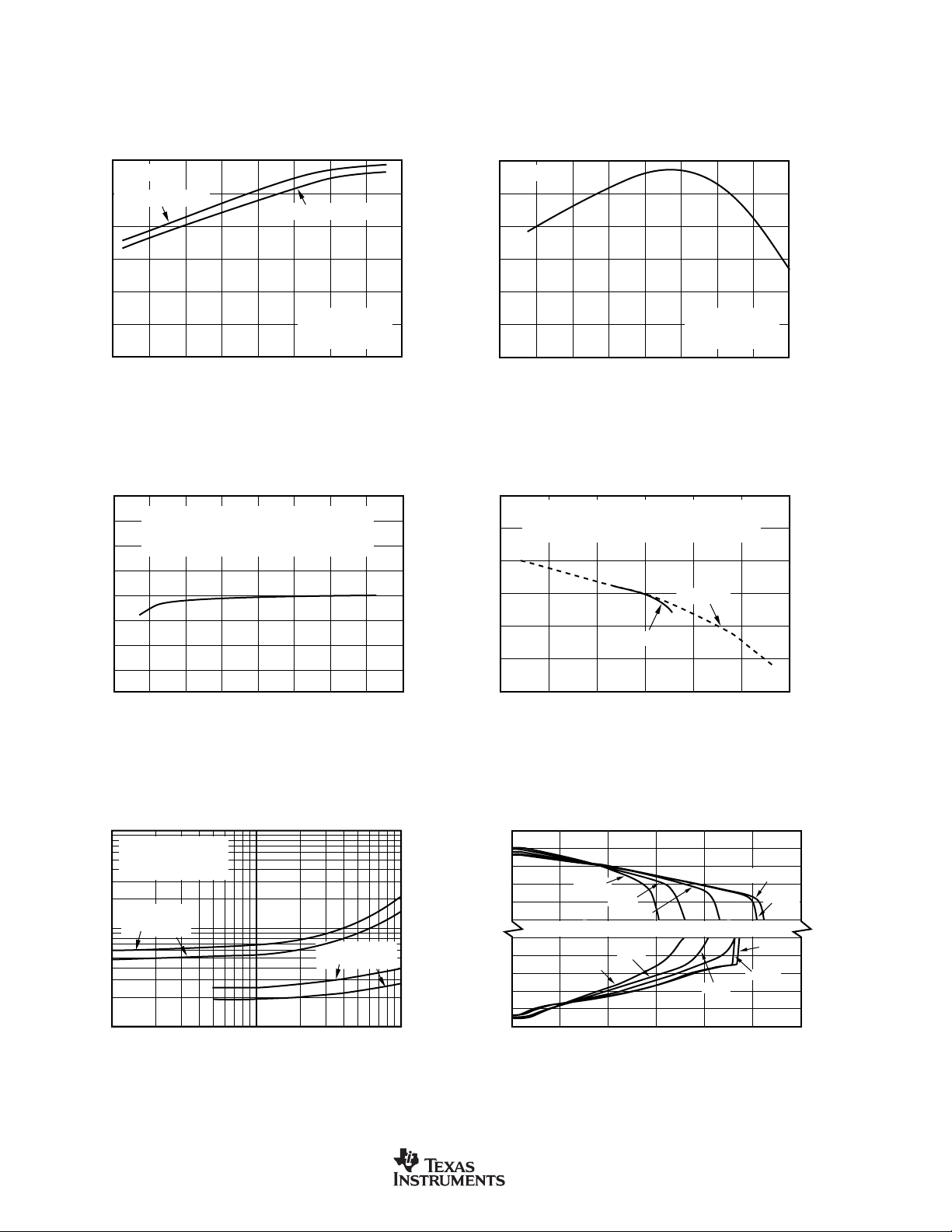
TYPICAL PERFORMANCE CURVES
0.1 101 100 1k 10k
100k
10k
1k
100
10
1
Voltage Noise (nV/√Hz)
Current Noise (fA/√Hz)
Frequency (Hz)
INPUT VOLTAGE AND CURRENT NOISE
SPECTRAL DENSITY vs FREQUENCY
Current Noise
Voltage Noise
At TA = +25°C, RL = 10kΩ, and VS = ±15V, unless otherwise noted.
OPEN-LOOP GAIN/PHASE vs FREQUENCY
OPA227
G
φ
0.01 0.10 1 10 100 1k 10k 100k 1M 10M 100M
Frequency (Hz)
POWER SUPPLY AND COMMON-MODE
REJECTION RATIO vs FREQUENCY
+CMRR
+PSRR
(dB)
OL
A
140
120
100
180
160
140
120
100
80
60
40
20
0
–20
80
0
–20
–40
–60
–80
–100
–120
–140
–160
–180
–200
180
160
140
120
100
(dB)
80
OL
A
Phase (°)
60
40
20
0
–20
OPEN-LOOP GAIN/PHASE vs FREQUENCY
OPA228
G
φ
0.01 0.10 1 10 100 1k 10k 100k 1M 10M 100M
Frequency (Hz)
0
–20
–40
–60
–80
–100
–120
–140
–160
–180
–200
Phase (°)
60
40
PSRR, CMRR (dB)
-20
–0
0.01
0.001
0.0001
THD+Noise (%)
0.00001
10.1 10 100 1k 10k 100k 1M
TOTAL HARMONIC DISTORTION + NOISE
G = 1, RL = 10kΩ
20 100 1k 10k 20k
–PSRR
Frequency (Hz)
vs FREQUENCY
V
= 3.5Vrms
OUT
Frequency (Hz)
OPA227
0.01
0.001
0.0001
THD+Noise (%)
0.00001
20 100 1k 10k 50k
TOTAL HARMONIC DISTORTION + NOISE
G = 1, RL = 10kΩ
vs FREQUENCY
V
= 3.5Vrms
OUT
Frequency (Hz)
OPA228
OPA227, 2227, 4227
OPA228, 2228, 4228
SBOS110A
www.ti.com
5
Page 6
TYPICAL PERFORMANCE CURVES (CONT)
At TA = +25°C, RL =10kΩ, and VS = ±15V, unless otherwise noted.
50nV/div
24
16
INPUT NOISE VOLTAGE vs TIME
1s/div
VOLTAGE NOISE DISTRIBUTION (10Hz)
140
120
100
80
Channel Separation (dB)
60
40
17.5
15.0
12.5
10.0
CHANNEL SEPARATION vs FREQUENCY
Dual and quad devices. G = 1, all channels.
Quad measured Channel A to D, or B to C;
other combinations yield similiar or improved
rejection.
10 100 1k 10k 100k 1M
Frequency (Hz)
OFFSET VOLTAGE PRODUCTION DISTRIBUTION
Typical distribution
of packaged units.
8
Percent of Units (%)
0
3.160 3.25 3.34 3.43 3.51 3.60 3.69 3.78
Noise (nV/√Hz)
OFFSET VOLTAGE DRIFT PRODUCTION DISTRIBUTION
12
8
4
Percent of Amplifiers (%)
0
0 0.5 1.0 1.5
Offset Voltage Drift (µV)/°C
Typical distribution
of packaged units.
5.5
5.0
Percent of Amplifiers (%)
2.5
0
0
–90
–75
–60
–150
–135
–120
–105
10
8
6
4
2
0
–2
–4
–6
Offset Voltage Change (µV)
–8
–10
0 100 150 300
WARM-UP OFFSET VOLTAGE DRIFT
50 200 250
Time from Power Supply Turn-On (s)
–45
Offset Voltage (µV)
–30
–15
1530456075
90
105
120
135
150
OPA227, 2227, 4227
6
www.ti.com
OPA228, 2228, 4228
SBOS110A
Page 7
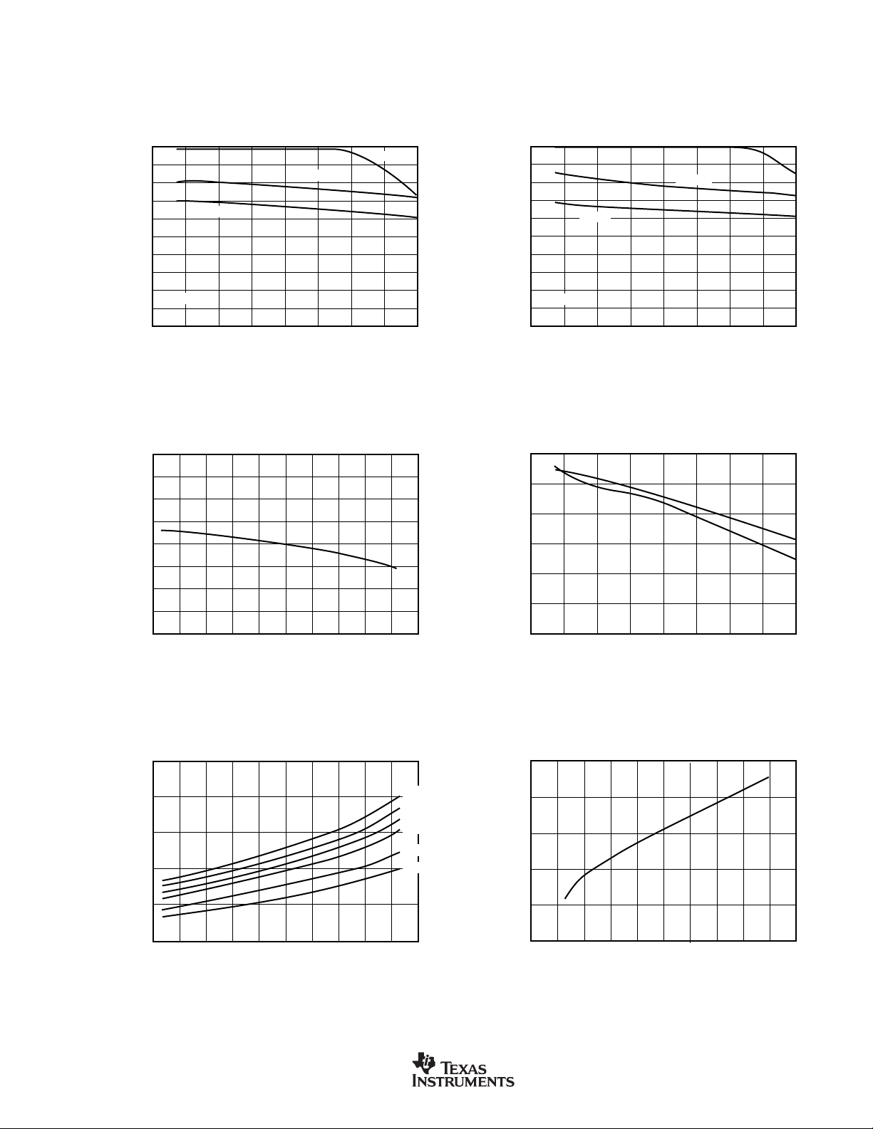
TYPICAL PERFORMANCE CURVES (CONT)
–75 –50 –25 0 25 50 75 100 125
60
50
40
30
20
10
0
Short-Circuit Current (mA)
Temperature (°C)
SHORT-CIRCUIT CURRENT vs TEMPERATURE
+I
SC
–I
SC
–75 –50 –25 0 25 50 75 100 125
160
150
140
130
120
110
100
90
80
70
60
A
OL
, CMRR, PSRR (dB)
Temperature (°C)
A
OL
, CMRR, PSRR vs TEMPERATURE
CMRR
PSRR
A
OL
OPA228
At TA = +25°C, RL = 10kΩ, and VS = ±15V, unless otherwise noted.
, CMRR, PSRR vs TEMPERATURE
A
OPA227
OL
PSRR
CMRR
Temperature (°C)
A
OL
160
150
140
130
120
110
100
, CMRR, PSRR (dB)
90
OL
A
80
70
60
–75 –50 –25 0 25 50 75 100 125
2.0
1.5
1.0
0.5
0
–0.5
–1.0
Input Bias Current (nA)
–1.5
–2.0
5.0
4.5
4.0
3.5
INPUT BIAS CURRENT vs TEMPERATURE
–60
–20 0 20 40 60 80 100 120 140
–40
QUIESCENT CURRENT vs TEMPERATURE
Temperature (°C)
±18V
±15V
±12V
±10V
±5V
±2.5V
3.8
QUIESCENT CURRENT vs SUPPLY VOLTAGE
3.6
3.4
3.2
Quiescent Current (mA)
3.0
2.5
–60 –40 –20 0 20 40 60 80
OPA227, 2227, 4227
OPA228, 2228, 4228
SBOS110A
Temperature (°C)
Quiescent Current (mA)
3.0
2.8
100 120 140
0 2 4 6 8 1012141618
Supply Voltage (±V)
www.ti.com
20
7
Page 8
TYPICAL PERFORMANCE CURVES (CONT)
At TA = +25°C, RL = 10kΩ, and VS = ±15V, unless otherwise noted.
3.0
SLEW RATE vs TEMPERATURE
OPA227
2.5
Positive Slew Rate
2.0
1.5
1.0
Slew Rate (µV/V)
0.5
0
–75 –50 –25 0 25 50 75 100
Temperature (°C)
CHANGE IN INPUT BIAS CURRENT
2.0
1.5
1.0
0.5
0
(nA)
B
∆I
–0.5
–1.0
–1.5
–2.0
0 5 10 15 20 25 30 35 40
vs POWER SUPPLY VOLTAGE
Curve shows normalized change in bias current
with respect to V
from –2nA to +2nA at V
= ±10V. Typical IB may range
S
Supply Voltage (V)
Negative Slew Rate
R
C
= ±10V.
S
LOAD
LOAD
= 2kΩ
= 100pF
125
12
SLEW RATE vs TEMPERATURE
OPA228
10
8
6
4
Slew Rate (µV/V)
2
0
–75 –50 –25 0 25 50 75 100
Temperature (°C)
CHANGE IN INPUT BIAS CURRENT
1.5
1.0
0.5
0
(nA)
B
∆I
–0.5
–1.0
–1.5
–15 –10 –50 510
vs COMMON-MODE VOLTAGE
Curve shows normalized change in bias current
with respect to VCM = 0V. Typical IB may range
from –2nA to +2nA at V
Common-Mode Voltage (V)
CM
VS = ±5V
= 0V.
R
C
LOAD
VS = ±15V
LOAD
= 2kΩ
= 100pF
125
15
100
SETTLING TIME vs CLOSED-LOOP GAIN
VS = ±15V, 10V Step
C
= 1500pF
L
R
= 2kΩ
L
OPA227
0.01%
10
Settling Time (µs)
1
±1 ±10 ±100
0.1%
Gain (V/V)
OPA228
0.01%
0.1%
Output Voltage Swing (V)
OUTPUT VOLTAGE SWING vs OUTPUT CURRENT
15
14
13
12
11
10
–10
–11
–12
–13
–14
–15
0 102030405060
125°C
85°C
125°C
Output Current (mA)
25°C
85°C
25°C
–40°C
–55°C
–55°C
–40°C
V+
(V+) –1V
(V+) –2V
(V+) –3V
(V–) +3V
(V–) +2V
(V–) +1V
V–
OPA227, 2227, 4227
8
www.ti.com
OPA228, 2228, 4228
SBOS110A
Page 9

TYPICAL PERFORMANCE CURVES (CONT)
SMALL-SIGNAL OVERSHOOT
vs LOAD CAPACITANCE
1k100101 10k 100k
Load Capacitance (pF)
70
60
50
40
30
20
10
0
Overshoot (%)
Gain = –10
Gain = +10
OPA227
Gain = +1
Gain = –1
At TA = +25°C, RL = 10kΩ, and VS = ±15V, unless otherwise noted.
MAXIMUM OUTPUT VOLTAGE vs FREQUENCY
30
25
20
15
10
Output Voltage (Vp-p)
5
VS = ±15V
VS = ±5V
OPA227
0
1k
2V/div
10k 100k 1M
Frequency (Hz)
LARGE-SIGNAL STEP RESPONSE
G = –1, C
= 1500pF
L
5µs/div
10M
OPA227
SMALL-SIGNAL STEP RESPONSE
G = +1, C
= 5pF
L
25mV/div
SMALL-SIGNAL STEP RESPONSE
G = +1, C
= 1000pF
L
400ns/div
OPA227
OPA227, 2227, 4227
OPA228, 2228, 4228
SBOS110A
25mV/div
400ns/div
www.ti.com
OPA227
9
Page 10

TYPICAL PERFORMANCE CURVES (CONT)
At TA = +25°C, RL = 10kΩ, and VS = ±15V, unless otherwise noted.
MAXIMUM OUTPUT VOLTAGE vs FREQUENCY
30
25
20
15
10
Output Voltage (Vp-p)
5
VS = ±5V
VS = ±15V
OPA228
70
60
50
40
30
Overshoot (%)
20
10
SMALL-SIGNAL OVERSHOOT
vs LOAD CAPACITANCE
OPA228
G = –100
G = +100
G = ±10
0
1k
5V/div
10k 100k
Frequency (Hz)
LARGE-SIGNAL STEP RESPONSE
G = –10, C
L
2µs/div
= 100pF
1M 10M
OPA228
SMALL-SIGNAL STEP RESPONSE
G = +10, C
= 5pF, RL = 1.8kΩ
L
0
200mV/div
OPA228
1k100101 100k10k
Load Capacitance (pF)
SMALL-SIGNAL STEP RESPONSE
G = +10, C
= 1000pF, RL = 1.8kΩ
L
500ns/div
OPA228
10
200mV/div
500ns/div
www.ti.com
OPA227, 2227, 4227
OPA228, 2228, 4228
SBOS110A
Page 11

APPLICATIONS INFORMATION
OPA227
20kΩ
0.1µF
0.1µF
2
1
7
8
6
3
4
V+
V–
Trim range exceeds
offset voltage specification
OPA227 and OPA228 single op amps only.
Use offset adjust pins only to
null offset voltage of op amp.
See text.
The OP A227 and OPA228 series are precision op amps with
very low noise. The OPA227 series is unity-gain stable with
a slew rate of 2.3V/µs and 8MHz bandwidth. The OPA228
series is optimized for higher-speed applications with gains
of 5 or greater, featuring a slew rate of 10V/µs and 33MHz
bandwidth. Applications with noisy or high impedance
power supplies may require decoupling capacitors close to
the device pins. In most cases, 0.1µF capacitors are adequate.
OFFSET VOLTAGE AND DRIFT
The OPA227 and OPA228 series have very low offset
voltage and drift. To achieve highest dc precision, circuit
layout and mechanical conditions should be optimized.
Connections of dissimilar metals can generate thermal potentials at the op amp inputs which can degrade the offset
voltage and drift. These thermocouple effects can exceed
the inherent drift of the amplifier and ultimately degrade its
performance. The thermal potentials can be made to cancel
by assuring that they are equal at both input terminals. In
addition:
• Keep thermal mass of the connections made to the two
input terminals similar.
• Locate heat sources as far as possible from the critical
input circuitry.
• Shield op amp and input circuitry from air currents such
as those created by cooling fans.
FIGURE 1. OPA227 Offset Voltage Trim Circuit.
amp. This adjustment should not be used to compensate for
offsets created elsewhere in the system since this can
introduce additional temperature drift.
INPUT PROTECTION
Back-to-back diodes (see Figure 2) are used for input protection on the OPA227 and OPA228. Exceeding the turn-on
threshold of these diodes, as in a pulse condition, can cause
current to flow through the input protection diodes due to the
amplifier’s finite slew rate. W ithout external current-limiting
resistors, the input devices can be destroyed. Sources of high
input current can cause subtle damage to the amplifier.
Although the unit may still be functional, important parameters such as input offset voltage, drift, and noise may shift.
OPERATING VOLTAGE
OPA227 and OPA228 series op amps operate from ±2.5V to
±18V supplies with excellent performance. Unlike most op
amps which are specified at only one supply voltage, the
OPA227 series is specified for real-world applications; a
single set of specifications applies over the ±5V to ±15V
supply range. Specifications are assured for applications
between ±5V and ±15V power supplies. Some applications
do not require equal positive and negative output voltage
swing. Power supply voltages do not need to be equal. The
OPA227 and OPA228 series can operate with as little as 5V
between the supplies and with up to 36V between the
supplies. For example, the positive supply could be set to
25V with the negative supply at –5V or vice-versa. In
addition, key parameters are assured over the specified
temperature range, –40°C to +85°C. Parameters which vary
significantly with operating voltage or temperature are shown
in the Typical Performance Curves.
OFFSET VOLTAGE ADJUSTMENT
The OPA227 and OPA228 series are laser-trimmed for
very low offset and drift so most applications will not
require external adjustment. However, the OPA227 and
OPA228 (single versions) provide offset voltage trim connections on pins 1 and 8. Offset voltage can be adjusted by
connecting a potentiometer as shown in Figure 1. This
adjustment should be used only to null the offset of the op
OPA227, 2227, 4227
OPA228, 2228, 4228
SBOS110A
FIGURE 2. Pulsed Operation.
When using the OP A227 as a unity-gain buffer (follower), the
input current should be limited to 20mA. This can be accomplished by inserting a feedback resistor or a resistor in series
with the source. Sufficient resistor size can be calculated:
where RX is either in series with the source or inserted in
the feedback path. For example, for a 10V pulse (VS =
10V), total loop resistance must be 500Ω. If the source
impedance is large enough to sufficiently limit the current
on its own, no additional resistors are needed. The size of
any external resistors must be carefully chosen since they
will increase noise. See the Noise Performance section of
this data sheet for further information on noise calculation. Figure 2 shows an example implementing a currentlimiting feedback resistor.
www.ti.com
R
500Ω
–
+
Input
RX = VS/20mA – R
F
OPA227
Output
SOURCE
11
Page 12

INPUT BIAS CURRENT CANCELLATION
VOLTAGE NOISE SPECTRAL DENSITY
vs SOURCE RESISTANCE
100k 10M
Source Resistance, R
S
(Ω)
100
1k 10k
1.00+03
1.00E+02
1.00E+01
1.00E+00
Votlage Noise Spectral Density, E
0
Typical at 1k (V/√Hz)
OPA227
OPA277
Resistor Noise
Resistor Noise
OPA277
OPA227
R
S
E
O
E
O
2
= e
n
2
+ (in RS)2 + 4kTR
S
The input bias current of the OPA227 and OPA228 series is
internally compensated with an equal and opposite cancellation current. The resulting input bias current is the difference
between with input bias current and the cancellation current.
The residual input bias current can be positive or negative.
When the bias current is cancelled in this manner, the input
bias current and input offset current are approximately equal.
A resistor added to cancel the effect of the input bias current
(as shown in Figure 3) may actually increase offset and noise
and is therefore not recommended.
Conventional Op Amp Configuration
R
2
R
1
Not recommended
for OPA227
Op Amp
NOISE PERFORMANCE
Figure 4 shows total circuit noise for varying source impedances with the op amp in a unity-gain configuration (no
feedback resistor network, therefore no additional noise contributions). T wo dif ferent op amps are shown with total circuit
noise calculated. The OPA227 has very low voltage noise,
making it ideal for low source impedances (less than 20kΩ).
A similar precision op amp, the OPA277, has somewhat higher
voltage noise but lower current noise. It provides excellent
noise performance at moderate source impedance (10kΩ to
100kΩ). Above 100kΩ, a FET-input op amp such as the
OPA132 (very low current noise) may provide improved
performance. The equation is shown for the calculation of the
total circuit noise. Note that e
= voltage noise, in = current
n
noise, RS = source impedance, k = Boltzmann’s constant =
1.38 • 10
–23
J/K and T is temperature in K. For more details on
calculating noise, see the insert titled “Basic Noise Calculations.”
RB = R2 || R
Recommended OPA227 Configuration
FIGURE 3. Input Bias Current Cancellation.
Design of low noise op amp circuits requires careful
consideration of a variety of possible noise contributors:
noise from the signal source, noise generated in the op
amp, and noise from the feedback network resistors. The
total noise of the circuit is the root-sum-square combination of all noise components.
The resistive portion of the source impedance produces
thermal noise proportional to the square root of the
resistance. This function is shown plotted in Figure 4.
Since the source impedance is usually fixed, select the op
amp and the feedback resistors to minimize their contribution to the total noise.
Figure 4 shows total noise for varying source impedances with the op amp in a unity-gain configuration (no
feedback resistor network and therefore no additional
noise contributions). The operational amplifier itself contributes both a voltage noise component and a current
12
External Cancellation Resistor
1
R
1
OPA227
R
2
No cancellation resistor.
See text.
FIGURE 4. Noise Performance of the OPA227 in Unity-
BASIC NOISE CALCULATIONS
noise component. The voltage noise is commonly modeled as a time-varying component of the offset voltage.
The current noise is modeled as the time-varying component of the input bias current and reacts with the source
resistance to create a voltage component of noise. Consequently, the lowest noise op amp for a given application
depends on the source impedance. For low source impedance, current noise is negligible and voltage noise generally dominates. For high source impedance, current noise
may dominate.
Figure 5 shows both inverting and noninverting op amp
circuit configurations with gain. In circuit configurations
with gain, the feedback network resistors also contribute
noise. The current noise of the op amp reacts with the
feedback resistors to create additional noise components.
www.ti.com
The feedback resistor values can generally be chosen to
make these noise sources negligible. The equations for
total noise are shown for both configurations.
Gain Buffer Configuration.
OPA227, 2227, 4227
OPA228, 2228, 4228
SBOS110A
Page 13

Noise in Noninverting Gain Configuration
R
2
R
1
R
S
V
S
Noise at the output:
2
E
11=+
On nSnS
E
O
Where eS = √4kTRS • = thermal noise of R
2
R
21222
2
eeeiReiR
+++
R
1
R
2
1
+
R
1
R
e1 = √4kTR1 • = thermal noise of R
2
R
1
2
2
()
++
2
()
2
S
1
2
R
2
+
R
1
e2 = √4kTR
Noise in Inverting Gain Configuration
R
2
R
1
E
R
S
O
Noise at the output:
2
E
1=+
O
RR
Where eS = √4kTRS • = thermal noise of R
V
S
e1 = √4kTR1 • = thermal noise of R
e2 = √4kTR
For the OPA227 and OPA228 series op amps at 1kHz, en = 3nV/√Hz and in = 0.4pA/√Hz.
2
2
R
2
+
1
2
+++
eeeiRe
nnS
S
RR
RR
2
= thermal noise of R
2
()
2
R
1
R
+
1
122
2
+
S
2
S
2
= thermal noise of R
2
2
+
S
1
2
FIGURE 5. Noise Calculation in Gain Configurations.
OPA227, 2227, 4227
OPA228, 2228, 4228
SBOS110A
www.ti.com
13
Page 14

R
2MΩ
R
1
2MΩ
2
R
8
402kΩ
R
11
178kΩ
C
1
1µF
Input from
Device
Under
Test
C
1µF
1kΩ
2
C
2
3
4
22nF
U2
(OPA227)
R
178kΩ
6
R
9
10
226kΩ
C
0.47µF
5
R
3
9.09kΩ
U1
R
5
634kΩ
R
4
(OPA227)
R
6
40.2kΩ
R
7
97.6kΩ
C
3
0.47µF
2
3
C
6
10nF
U3
(OPA227)
FIGURE 6. 0.1Hz to 10Hz Bandpass Filter Used to Test Wideband Noise of the OPA227 and OPA228 Series.
USING THE OPA228 IN LOW GAINS
The OPA228 family is intended for applications with signal
22pF
gains of 5 or greater, but it is possible to take advantage of
their high speed in lower gains. Without external compensation, the OPA228 has sufficient phase margin to maintain
10Ω
2
3
100kΩ
OPA227
Device
Under
Test
6
V
OUT
stability in unity gain with purely resistive loads. However,
the addition of load capacitance can reduce the phase
margin and destabilize the op amp.
A variety of compensation techniques have been evaluated
specifically for use with the OPA228. The recommended
configuration consists of an additional capacitor (CF) in
parallel with the feedback resistance, as shown in Figures
8 and 11. This feedback capacitor serves two purposes in
compensating the circuit. The op amp’s input capacitance
FIGURE 7. Noise Test Circuit.
and the feedback resistors interact to cause phase shift that
can result in instability. CF compensates the input capaci-
Figure 6 shows the 0.1Hz 10Hz bandpass filter used to test
the noise of the OP A227 and OPA228. The filter circuit was
designed using T exas Instruments’ FilterPro software (available at www.ti.com). Figure 7 shows the configuration of
the OPA227 and OPA228 for noise testing.
tance, minimizing peaking. Additionally, at high frequencies, the closed-loop gain of the amplifier is strongly
influenced by the ratio of the input capacitance and the
feedback capacitor. Thus, CF can be selected to yield good
stability while maintaining high speed.
6
V
OUT
14
www.ti.com
OPA227, 2227, 4227
OPA228, 2228, 4228
SBOS110A
Page 15

Without external compensation, the noise specification of
the OPA228 is the same as that for the OPA227 in gains of
5 or greater. With the additional external compensation, the
output noise of the of the OPA228 will be higher. The
amount of noise increase is directly related to the increase
in high frequency closed-loop gain established by the CIN/
CF ratio.
Figures 8 and 11 show the recommended circuit for gains
of +2 and –2, respectively. The figures suggest approximate
values for CF. Because compensation is highly dependent
on circuit design, board layout, and load conditions, C
should be optimized experimentally for best results. Figures 9 and 10 show the large- and small-signal step responses for the G = +2 configuration with 100pF load
capacitance. Figures 12 and 13 show the large- and smallsignal step responses for the G = –2 configuration with
100pF load capacitance.
F
22pF
2kΩ
2kΩ
OPA228
2kΩ
100pF
FIGURE 8. Compensation of the OPA228 for G =+2.
5mV/div
15pF
1kΩ 2kΩ
OPA228
2kΩ
100pF
FIGURE 11. Compensation for OPA228 for G = –2.
5mV/div
OPA228
400ns/div
FIGURE 9. Large-Signal Step Response, G = +2, C
100pF, Input Signal = 5Vp-p.
25mV/div
OPA228
200ns/div
FIGURE 10. Small-Signal Step Response, G = +2, C
100pF, Input Signal = 50mVp-p.
OPA227, 2227, 4227
OPA228, 2228, 4228
SBOS110A
=
LOAD
=
LOAD
www.ti.com
OPA228
400ns/div
FIGURE 12. Large-Signal Step Response, G = –2, C
100pF, Input Signal = 5Vp-p.
25mV/div
OPA228
200ns/div
FIGURE 13. Small-Signal Step Response, G = –2, C
100pF, Input Signal = 50mVp-p.
LOAD
LOAD
=
=
15
Page 16

1.1kΩ
2.2nF
V
IN
1.65kΩ1.1kΩ
33nF
OPA227
1.43kΩ
1.91kΩ
68nF
1.43kΩ
330pF
OPA227
2.21kΩ
dc Gain = 1
10nF
V
OUT
fN = 13.86kHz
Q = 1.186
FIGURE 14. Three-Pole, 20kHz Low Pass, 0.5dB Chebyshev Filter.
0.1µF
100Ω 100kΩ
2
OPA227
3
Dexter 1M
Thermopile
Detector
Responsivity ≈ 2.5 x 10
Output Noise ≈ 30µVrms, 0.1Hz to 10Hz
NOTE: Use metal film resistors
and plastic film capacitor. Circuit
must be well shielded to achieve
low noise.
4
6
V/W
Output
TTL INPUT
“1”
“0”
Input
TTL
In
fN = 20.33kHz f = 7.2kHz
Q = 4.519
20pF
D1
D2
DG188
GAIN
+1
–1
10kΩ
4.99kΩ
S1
S2
2
OPA227
3
1
Offset
Trim
9.76kΩ
4.75kΩ
1kΩ
+V
500Ω
6
8
CC
Balance
Trim
Output
4.75kΩ
FIGURE 15. Long-Wavelength Infrared Detector Amplifier.
16
FIGURE 16. High Performance Synchronous Demodulator.
www.ti.com
OPA227, 2227, 4227
OPA228, 2228, 4228
SBOS110A
Page 17

+15V
0.1µF
1kΩ
Audio
In
This application uses two op amps
in parallel for higher output current drive.
FIGURE 17. Headphone Amplifier.
R
1
7.5kΩ
1kΩ
Bass Tone Control
R
50kΩ
CW
2
1/2
OPA2227
1/2
OPA2227
–15V
13
0.1µF
R
3
7.5kΩ
200Ω
200Ω
To
Headphone
2
R
10
100kΩ
Midrange Tone Control
C
1
940pF
R
R
4
V
IN
2.7kΩ
50kΩ
CW
5
13
2
R
6
2.7kΩ
C
2
0.0047µF
Treble Tone Control
R
R
7.5kΩ
7
50kΩ
CW
8
13
2
R
9
7.5kΩ
C
680pF
R
11
100kΩ
3
2
OPA227
3
6
V
OUT
FIGURE 18. Three-Band ActiveTone Control (bass, midrange and treble).
OPA227, 2227, 4227
OPA228, 2228, 4228
SBOS110A
www.ti.com
17
Page 18

PACKAGE OPTION ADDENDUM
www.ti.com
PACKAGING INFORMATION
Orderable Device Status
OPA2227P ACTIVE PDIP P 8 50 Green (RoHS &
OPA2227PA ACTIVE PDIP P 8 50 Green (RoHS &
OPA2227PAG4 ACTIVE PDIP P 8 50 Green (RoHS &
OPA2227U ACTIVE SOIC D 8 100 Green (RoHS &
OPA2227U/2K5 ACTIVE SOIC D 8 2500 Green (RoHS &
OPA2227U/2K5E4 ACTIVE SOIC D 8 2500 Pb-Free
OPA2227U/2K5G4 ACTIVE SOIC D 8 2500 Green (RoHS &
OPA2227UA ACTIVE SOIC D 8 100 Green (RoHS &
OPA2227UA/2K5 ACTIVE SOIC D 8 2500 Pb-Free
OPA2227UA/2K5E4 ACTIVE SOIC D 8 2500 Green (RoHS &
OPA2227UAE4 ACTIVE SOIC D 8 100 Green (RoHS &
OPA2227UAG4 ACTIVE SOIC D 8 100 Green (RoHS &
OPA2227UE4 ACTIVE SOIC D 8 100 Pb-Free
OPA2227UG4 ACTIVE SOIC D 8 100 Green (RoHS &
OPA2228P ACTIVE PDIP P 8 50 Green (RoHS &
OPA2228PA ACTIVE PDIP P 8 50 Green (RoHS &
OPA2228PG4 ACTIVE PDIP P 8 50 Green (RoHS &
OPA2228U ACTIVE SOIC D 8 100 Pb-Free
OPA2228U/2K5 ACTIVE SOIC D 8 2500 Pb-Free
OPA2228UA ACTIVE SOIC D 8 100 Pb-Free
OPA2228UA/2K5 ACTIVE SOIC D 8 2500 Pb-Free
OPA227P ACTIVE PDIP P 8 50 Green (RoHS &
OPA227PA ACTIVE PDIP P 8 50 Green (RoHS &
OPA227PAG4 ACTIVE PDIP P 8 50 Green (RoHS &
OPA227U ACTIVE SOIC D 8 100 Pb-Free
(1)
Package
Type
Package
Drawing
Pins Package
Qty
Eco Plan
no Sb/Br)
no Sb/Br)
no Sb/Br)
no Sb/Br)
no Sb/Br)
(RoHS)
no Sb/Br)
no Sb/Br)
(RoHS)
no Sb/Br)
no Sb/Br)
no Sb/Br)
(RoHS)
no Sb/Br)
no Sb/Br)
no Sb/Br)
no Sb/Br)
(RoHS)
(RoHS)
(RoHS)
(RoHS)
no Sb/Br)
no Sb/Br)
no Sb/Br)
(RoHS)
(2)
Lead/Ball Finish MSL Peak Temp
CU NIPDAU N / A for Pkg Type
CU NIPDAU N / A for Pkg Type
CU NIPDAU N / A for Pkg Type
CU NIPDAU Level-3-260C-168 HR
CU NIPDAU Level-3-260C-168 HR
CU NIPDAU Level-3-260C-168 HR
CU NIPDAU Level-3-260C-168 HR
CU NIPDAU Level-3-260C-168 HR
CU NIPDAU Level-3-260C-168 HR
CU NIPDAU Level-3-260C-168 HR
CU NIPDAU Level-3-260C-168 HR
CU NIPDAU Level-3-260C-168 HR
CU NIPDAU Level-3-260C-168 HR
CU NIPDAU Level-3-260C-168 HR
CU NIPDAU N / A for Pkg Type
CU NIPDAU N / A for Pkg Type
CU NIPDAU N / A for Pkg Type
CU NIPDAU Level-3-260C-168 HR
CU NIPDAU Level-3-260C-168 HR
CU NIPDAU Level-3-260C-168 HR
CU NIPDAU Level-3-260C-168 HR
CU NIPDAU N / A for Pkg Type
CU NIPDAU N / A for Pkg Type
CU NIPDAU N / A for Pkg Type
CU NIPDAU Level-3-260C-168 HR
12-Sep-2006
(3)
Addendum-Page 1
Page 19

PACKAGE OPTION ADDENDUM
www.ti.com
Orderable Device Status
(1)
Package
Type
Package
Drawing
Pins Package
Qty
Eco Plan
OPA227U/2K5 ACTIVE SOIC D 8 2500 Pb-Free
(2)
Lead/Ball Finish MSL Peak Temp
CU NIPDAU Level-3-260C-168 HR
12-Sep-2006
(3)
(RoHS)
OPA227UA ACTIVE SOIC D 8 100 Green (RoHS &
CU NIPDAU Level-3-260C-168 HR
no Sb/Br)
OPA227UA/2K5 ACTIVE SOIC D 8 2500 Green (RoHS &
CU NIPDAU Level-3-260C-168 HR
no Sb/Br)
OPA227UA/2K5G4 ACTIVE SOIC D 8 2500 Green (RoHS &
CU NIPDAU Level-3-260C-168 HR
no Sb/Br)
OPA227UAG4 ACTIVE SOIC D 8 100 Green (RoHS &
CU NIPDAU Level-3-260C-168 HR
no Sb/Br)
OPA228P ACTIVE PDIP P 8 50 Green (RoHS &
CU NIPDAU N / A for Pkg Type
no Sb/Br)
OPA228PA ACTIVE PDIP P 8 50 Green (RoHS &
CU NIPDAU N / A for Pkg Type
no Sb/Br)
OPA228PG4 ACTIVE PDIP P 8 50 Green (RoHS &
CU NIPDAU N / A for Pkg Type
no Sb/Br)
OPA228U ACTIVE SOIC D 8 100 Green (RoHS &
CU NIPDAU Level-3-260C-168 HR
no Sb/Br)
OPA228UA ACTIVE SOIC D 8 100 Green (RoHS &
CU NIPDAU Level-3-260C-168 HR
no Sb/Br)
OPA228UA/2K5 ACTIVE SOIC D 8 2500 Pb-Free
CU NIPDAU Level-3-260C-168 HR
(RoHS)
OPA228UAG4 ACTIVE SOIC D 8 100 Green (RoHS &
CU NIPDAU Level-3-260C-168 HR
no Sb/Br)
OPA228UG4 ACTIVE SOIC D 8 100 Green (RoHS &
CU NIPDAU Level-3-260C-168 HR
no Sb/Br)
OPA4227PA ACTIVE PDIP N 14 25 Green (RoHS &
CU NIPDAU N / A for Pkg Type
no Sb/Br)
OPA4227PAG4 ACTIVE PDIP N 14 25 Green (RoHS &
CU NIPDAU N / A for Pkg Type
no Sb/Br)
OPA4227UA ACTIVE SOIC D 14 58 Green (RoHS &
CU NIPDAU Level-3-260C-168 HR
no Sb/Br)
OPA4227UA/2K5 ACTIVE SOIC D 14 2500 Green (RoHS &
CU NIPDAU Level-3-260C-168 HR
no Sb/Br)
OPA4227UA/2K5G4 ACTIVE SOIC D 14 2500 Green (RoHS &
CU NIPDAU Level-3-260C-168 HR
no Sb/Br)
OPA4228PA ACTIVE PDIP N 14 25 Green (RoHS &
CU NIPDAU N / A for Pkg Type
no Sb/Br)
OPA4228UA ACTIVE SOIC D 14 58 Pb-Free
CU NIPDAU Level-3-260C-168 HR
(RoHS)
OPA4228UA/2K5 ACTIVE SOIC D 14 2500 Pb-Free
CU NIPDAU Level-3-260C-168 HR
(RoHS)
(1)
The marketing status values are defined as follows:
ACTIVE: Product device recommended for new designs.
LIFEBUY: TI has announced that the device will be discontinued, and a lifetime-buy period is in effect.
NRND: Not recommended for new designs. Device is in production to support existing customers, but TI does not recommend using this part in
a new design.
PREVIEW: Device has been announced but is not in production. Samples may or may not be available.
OBSOLETE: TI has discontinued the production of the device.
(2)
Eco Plan - The planned eco-friendly classification: Pb-Free (RoHS), Pb-Free (RoHS Exempt), or Green (RoHS & no Sb/Br) - please check
http://www.ti.com/productcontent for the latest availability information and additional product content details.
Addendum-Page 2
Page 20

PACKAGE OPTION ADDENDUM
www.ti.com
TBD: The Pb-Free/Green conversion plan has not been defined.
Pb-Free (RoHS): TI's terms "Lead-Free" or "Pb-Free" mean semiconductor products that are compatible with the current RoHS requirements
for all 6 substances, including the requirement that lead not exceed 0.1% by weight in homogeneous materials. Where designed to be soldered
at high temperatures, TI Pb-Free products are suitable for use in specified lead-free processes.
Pb-Free (RoHS Exempt): This component has a RoHS exemption for either 1) lead-based flip-chip solder bumps used between the die and
package, or 2) lead-based die adhesive used between the die and leadframe. The component is otherwise considered Pb-Free (RoHS
compatible) as defined above.
Green (RoHS & no Sb/Br): TI defines "Green" to mean Pb-Free (RoHS compatible), and free of Bromine (Br) and Antimony (Sb) based flame
retardants (Br or Sb do not exceed 0.1% by weight in homogeneous material)
(3)
MSL, Peak Temp. -- The Moisture Sensitivity Level rating according to the JEDEC industry standard classifications, and peak solder
temperature.
Important Information and Disclaimer:The information provided on this page represents TI's knowledge and belief as of the date that it is
provided. TI bases its knowledge and belief on information provided by third parties, and makes no representation or warranty as to the
accuracy of such information. Efforts are underway to better integrate information from third parties. TI has taken and continues to take
reasonable steps to provide representative and accurate information but may not have conducted destructive testing or chemical analysis on
incoming materials and chemicals. TI and TI suppliers consider certain information to be proprietary, and thus CAS numbers and other limited
information may not be available for release.
In no event shall TI's liability arising out of such information exceed the total purchase price of the TI part(s) at issue in this document sold by TI
to Customer on an annual basis.
12-Sep-2006
Addendum-Page 3
Page 21

MECHANICAL DATA
MPDI001A – JANUARY 1995 – REVISED JUNE 1999
P (R-PDIP-T8) PLASTIC DUAL-IN-LINE
0.400 (10,60)
0.355 (9,02)
8
5
0.260 (6,60)
0.240 (6,10)
1
0.021 (0,53)
0.015 (0,38)
NOTES: A. All linear dimensions are in inches (millimeters).
B. This drawing is subject to change without notice.
C. Falls within JEDEC MS-001
4
0.070 (1,78) MAX
0.020 (0,51) MIN
0.200 (5,08) MAX
0.125 (3,18) MIN
0.100 (2,54)
0.010 (0,25)
Seating Plane
M
0.325 (8,26)
0.300 (7,62)
0.015 (0,38)
Gage Plane
0.010 (0,25) NOM
0.430 (10,92)
MAX
4040082/D 05/98
For the latest package information, go to http://www.ti.com/sc/docs/package/pkg_info.htm
POST OFFICE BOX 655303 • DALLAS, TEXAS 75265
Page 22

Page 23

Page 24

Page 25

IMPORTANT NOTICE
Texas Instruments Incorporated and its subsidiaries (TI) reserve the right to make corrections, modifications,
enhancements, improvements, and other changes to its products and services at any time and to discontinue
any product or service without notice. Customers should obtain the latest relevant information before placing
orders and should verify that such information is current and complete. All products are sold subject to TI’s terms
and conditions of sale supplied at the time of order acknowledgment.
TI warrants performance of its hardware products to the specifications applicable at the time of sale in
accordance with TI’s standard warranty. Testing and other quality control techniques are used to the extent TI
deems necessary to support this warranty . Except where mandated by government requirements, testing of all
parameters of each product is not necessarily performed.
TI assumes no liability for applications assistance or customer product design. Customers are responsible for
their products and applications using TI components. To minimize the risks associated with customer products
and applications, customers should provide adequate design and operating safeguards.
TI does not warrant or represent that any license, either express or implied, is granted under any TI patent right,
copyright, mask work right, or other TI intellectual property right relating to any combination, machine, or process
in which TI products or services are used. Information published by TI regarding third-party products or services
does not constitute a license from TI to use such products or services or a warranty or endorsement thereof.
Use of such information may require a license from a third party under the patents or other intellectual property
of the third party, or a license from TI under the patents or other intellectual property of TI.
Reproduction of information in TI data books or data sheets is permissible only if reproduction is without
alteration and is accompanied by all associated warranties, conditions, limitations, and notices. Reproduction
of this information with alteration is an unfair and deceptive business practice. TI is not responsible or liable for
such altered documentation.
Resale of TI products or services with statements different from or beyond the parameters stated by TI for that
product or service voids all express and any implied warranties for the associated TI product or service and
is an unfair and deceptive business practice. TI is not responsible or liable for any such statements.
Following are URLs where you can obtain information on other Texas Instruments products and application
solutions:
Products Applications
Amplifiers amplifier.ti.com Audio www.ti.com/audio
Data Converters dataconverter.ti.com Automotive www.ti.com/automotive
DSP dsp.ti.com Broadband www.ti.com/broadband
Interface interface.ti.com Digital Control www.ti.com/digitalcontrol
Logic logic.ti.com Military www.ti.com/military
Power Mgmt power.ti.com Optical Networking www.ti.com/opticalnetwork
Microcontrollers microcontroller.ti.com Security www.ti.com/security
Low Power Wireless www.ti.com/lpw Telephony www.ti.com/telephony
Video & Imaging www.ti.com/video
Wireless www.ti.com/wireless
Mailing Address: Texas Instruments
Post Office Box 655303 Dallas, Texas 75265
Copyright 2006, Texas Instruments Incorporated
 Loading...