

Page 1
VIOmax
CHIP FORM
OP07C, OP07D, OP07Y
PRECISION OPERATIONAL AMPLIFIERS
SLOS099B – OCTOBER 1983 – REVISED AUGUST 1996
D
Low Noise
D
No External Components Required
D
Replaces Chopper Amplifiers at a Lower
Cost
D
Single-Chip Monolithic Fabrication
D
Wide Input Voltage Range
OFFSET N1
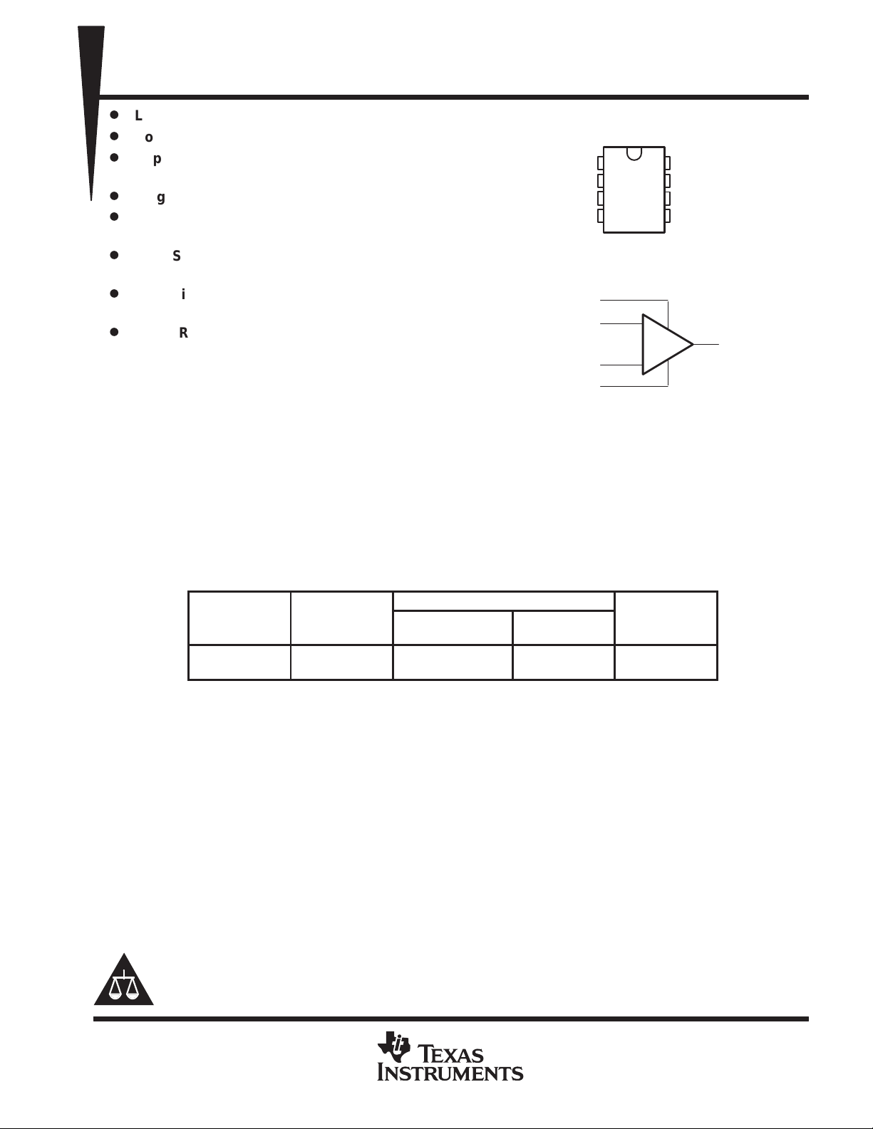
D OR P PACKAGE
(TOP VIEW)
1
IN–
2
IN+
3
V
CC–
4
OFFSET N2
8
V
7
CC+
OUT
6
NC
5
0 to ±14 V Typ
D
Wide Supply Voltage Range
±3 V to ±18 V
D
Essentially Equivalent to Fairchild µA714
Operational Amplifiers
D
Direct Replacement for PMI OP07C and
OP07D
description
symbol
NC–No internal connection
IN
IN –
1
3
+
+
2
–
8
OFFSET N1
OFFSET N2
6
OUT
These devices represent a breakthrough in operational amplifier performance. Low offset and long-term stability
are achieved by means of a low-noise, chopperless, bipolar-input-transistor amplifier circuit. For most
applications, external components are not required for offset nulling and frequency compensation. The true
differential input, with a wide input voltage range and outstanding common-mode rejection, provides maximum
flexibility and performance in high-noise environments and in noninverting applications. Low bias currents and
extremely high input impedances are maintained over the entire temperature range. The OP07 is unsurpassed
for low-noise, high-accuracy amplification of very low-level signals.
These devices are characterized for operation from 0°C to 70°C.
AVAILABLE OPTIONS
PACKAGED DEVICES
T
A
0°C to 70°C 150 µV
The D package is available taped and reeled. Add the suffix R to the device type (e.g., OP07CDR). The chip
form is tested at TA = 25°C.
AT 25°C
SMALL OUTLINE
(D)
OP07CD
OP07DD
PLASTIC DIP
(P)
OP07CP
OP07DP
(Y)
OP07Y
Please be aware that an important notice concerning availability, standard warranty, and use in critical applications of
Texas Instruments semiconductor products and disclaimers thereto appears at the end of this data sheet.
PRODUCTION DATA information is current as of publication date.
Products conform to specifications per the terms of Texas Instruments
standard warranty. Production processing does not necessarily include
testing of all parameters.
POST OFFICE BOX 655303 • DALLAS, TEXAS 75265
Copyright 1996, Texas Instruments Incorporated
1
Page 2
OP07C, OP07D, OP07Y
PRECISION OPERATIONAL AMPLIFIERS
SLOS099B – OCTOBER 1983 – REVISED AUGUST 1996
OP07Y chip information
These chips, properly assembled, display characteristics similar to the OP07. Thermal compression or
ultrasonic bonding may be used on the doped-aluminum bonding pads. Chips may be mounted with conductive
epoxy or a gold-silicon preform.
72
(8)
BONDING PAD ASSIGNMENTS
(7)
(2)
94
IN
IN –
(1)
(3)
+
(2)
(8)
OFFSET N1
(6)
OFFSET N2
CHIP THICKNESS: 15 TYPICAL
BONDING PADS: 4 × 4 MINIMUM
TJmax = 150°C
TOLERANCES ARE ± 10%.
ALL DIMENSIONS ARE IN MILS.
(3)(1)
(4)
PIN (4) IS INTERNALLY CONNECTED
TO BACKSIDE OF CHIP.
V
CC+
(7)
+
–
V
CC–
(4)
(6)
OUT
2
POST OFFICE BOX 655303 • DALLAS, TEXAS 75265
Page 3
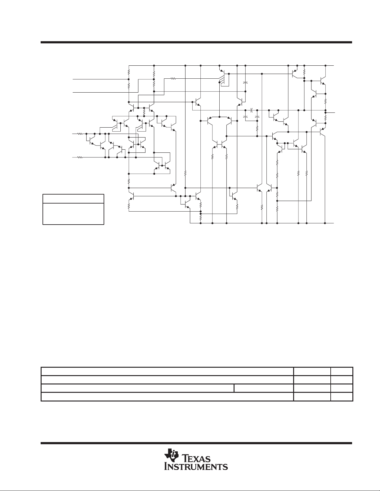
schematic
OFFSET N1
OP07C, OP07D, OP07Y
PRECISION OPERATIONAL AMPLIFIERS
SLOS099B – OCTOBER 1983 – REVISED AUGUST 1996
7
V
CC +
1
IN +
IN –
8
6
OUT
3
2
28
39
4
4
V
CC –
OFFSET N2
COMPONENT COUNT
Resistors
Transistors
Capacitors
absolute maximum ratings over operating free-air temperature range (unless otherwise noted)
Supply voltage, V
Supply voltage, V
Differential input voltage (see Note 2) ±30 V. . . . . . . . . . . . . . . . . . . . . . . . . . . . . . . . . . . . . . . . . . . . . . . . . . . . . . . .
Input voltage, V
Duration of output short circuit (see Note 4) unlimited. . . . . . . . . . . . . . . . . . . . . . . . . . . . . . . . . . . . . . . . . . . . . . .
Continuous total dissipation at (or below) 25°C free-air temperature (see Note 5) 500 mW. . . . . . . . . . . . . . . .
Operating free-air temperature range, T
Storage temperature range –65°C to 150°C. . . . . . . . . . . . . . . . . . . . . . . . . . . . . . . . . . . . . . . . . . . . . . . . . . . . . . . .
Lead temperature 1,6 mm (1/16 inch) from case for 10 seconds 260°C. . . . . . . . . . . . . . . . . . . . . . . . . . . . . . .
NOTES: 1. All voltage values, unless otherwise noted, are with respect to the midpoint between V
2. Differential voltages are at IN+ with respect to IN–.
3. The magnitude of the input voltage must never exceed the magnitude of the supply voltage or 15 V, whichever is less.
4. The output may be shorted to ground or either power supply.
5. For operation above 64°C free-air temperature, derate the D package to 464 mW at 70°C at the rate of 5.8 mW/°C.
(see Note 1) 22 V. . . . . . . . . . . . . . . . . . . . . . . . . . . . . . . . . . . . . . . . . . . . . . . . . . . . . . . . . . .
CC+
–22 V. . . . . . . . . . . . . . . . . . . . . . . . . . . . . . . . . . . . . . . . . . . . . . . . . . . . . . . . . . . . . . . . . . . . .
CC–
(either input, see Note 3) ±22 V. . . . . . . . . . . . . . . . . . . . . . . . . . . . . . . . . . . . . . . . . . . . . . . . . . . .
I
0°C to 70°C. . . . . . . . . . . . . . . . . . . . . . . . . . . . . . . . . . . . . . . . . . . . . .
A
CC+
and V
CC–
.
recommended operating conditions
Supply voltage, V
Common-mode input voltage, V
Operating free-air temperature, T
CC±
IC
A
POST OFFICE BOX 655303 • DALLAS, TEXAS 75265
MIN MAX UNIT
±3 ±18 V
V
= ±15 V –13 13 V
CC±
0 70 °C
3
Page 4

PRECISION OPERATIONAL AMPLIFIERS
PARAMETER
TEST CONDITIONS
†
T
UNIT
VIOInput offset voltage
V
R
Ω
V
IIOInput offset current
nA
IIBInput bias current
nA
V
Common-mode input voltge range
V
VOMPeak output voltage
V
V
±10 V
R
2 kΩ
CMRR
Common-mode rejection ratio
V
±13 V
R
Ω
dB
k
Suppl
oltage sensitivity (∆VIO/∆VCC)
CC±
,
V/V
4
electrical characteristics at specified free-air temperature, VCC ± = ±15 V (unless otherwise noted)
SLOS099B – OCTOBER 1983 – REVISED AUGUST 1996
OP07C, OP97D, OP07Y
POST OFFICE BOX 655303 DALLAS, TEXAS 75265
•
A
p
α
VIO
α
IIO
α
IIB
ICR
A
VD
B
1
r
i
SVS
P
D
†
All characteristics are measured under open-loop conditions with zero common-mode input voltage unless otherwise noted.
NOTE 6: Since long-term drift cannot be measured on the individual devices prior to shipment, this specification is not intended to be a warranty. It is an engineering estimate of the
Temperature coefficient of input offset voltage VO = 0, RS = 50 Ω 0°C to 70°C 0.5 1.8 0.7 2.5 µV/°C
Long-term drift of input offset voltage See Note 6 0.4 0.5 µV/mo
Offset adjustment range RS = 20 kΩ, See Figure 1 25°C ±4 ±4 mV
p
Temperature coefficient of input offset current 0°C to 70°C 12 50 12 50 pA/°C
p
Temperature coefficient of input bias current 0°C to 70°C 18 50 18 50 pA/°C
p
p
Large-signal differential voltage amplification
Unity-gain bandwidth 25°C 0.4 0.6 0.4 0.6 MHz
Input resistance 25°C 8 33 7 31 MΩ
pp
y v
Power dissipation
averaged trend line of drift versus time over extended periods after the first thirty days of operation.
= 0,
O
RL ≥ 10 kΩ ±12 ±13 ±12 ±13
RL ≥ 2 kΩ
RL ≥ 1 kΩ ±12 ±12
RL ≥ 2 kΩ 0°C to 70°C ±11 ±12.6 ±11 ± 12.6
V
= ±3 V ,
CC±
RL ≥ 500 kΩ
=
O
=
IC
V
= ±3 V to ±18 V,
RS = 50 Ω
VO = 0, No load 80 150 80 150
V
= ±3 V,
CC±
No load
,
,
= 50
S
VO = ±0.5 V,
=
L
= 50
S
VO = 0,
25°C 60 150 60 150
0°C to 70°C 85 250 85 250
25°C 0.8 6 0.8 6
0°C to 70°C 1.6 8 1.6 8
25°C ±1.8 ±7 ±2 ±12
0°C to 70°C ±2.2 ±9 ±3 ±14
25°C ±13 ±14 ±13 ±14
0°C to 70°C ±13 ±13.5 ±13 ±13.5
25°C
25°C 100 400 400
25°C 120 400 120 400
0°C to 70°C 100 400 100 400
25°C 100 120 94 110
0°C to 70°C 97 120 94 106
25°C 7 32 7 32
0°C to 70°C 10 51 10 51
25°C
OP07C OP07D
MIN TYP MAX MIN TYP MAX
±11.5 ±12.8 ±11.5 ±12.8
4 8 4 8
µ
V/mV
µ
mW
Page 5
PARAMETER
UNIT
PARAMETER
TEST CONDITIONS
†
UNIT
AVDLarge-signal differential voltage amplification
PDPower dissipation
MΩ
OP07C, OP07D, OP07Y
PRECISION OPERATIONAL AMPLIFIERS
SLOS099B – OCTOBER 1983 – REVISED AUGUST 1996
operating characteristics, V
V
n
V
N(PP)
I
n
I
N(PP)
SR Slew rate RL≥ 2 kΩ 0.3 0.3 V/µs
†
All characteristics are measured under open-loop conditions with zero common-mode input voltage unless otherwise noted.
Equivalent input noise voltage
Peak-to-peak equivalent input noise voltage f = 0.1 Hz to 10 Hz 0.38 0.38 µV
Equivalent input noise current
Peak-to-peak equivalent input noise current f = 0.1 Hz to 10 Hz 15 15 pA
electrical characteristics, V
V
I
IO
I
IB
V
V
B
r
i
CMRR Common-mode input resistance VIC = ±13 V, RS = 50 Ω 94 110 dB
k
NOTE 6: Since long-term drift cannot be measured on the individual devices prior to shipment, this specification is not intended to be a warranty .
Input offset voltage RS = 50 Ω 60 150 µV
IO
Long-term drift of input offset voltage See Note 6 0.5 µV/mo
Offset adjustment range RS = 20 kΩ, See Figure 1 ±4 mV
Input offset current 0.8 6 nA
Input bias current ±2 ±12 nA
Common-mode input voltage range ±13 ±14 V
ICR
Peak output voltage
OM
Unity-gain bandwidth 0.4 0.6 MHz
1
Input resistance 7 31 MΩ
Supply-voltage rejection ratio (∆VCC/∆VIO) V
SVS
p
It is an engineering estimate of the averaged trend line of drift versus time over extended periods after the first thirty days of operation.
CC
CC
=
±
=
±
p
±15 V, T
±15 V, T
RL ≤ 10 kΩ ±12 ±13
RL ≤ 2 kΩ
RL ≤ 1 kΩ ±12
V
VO = ±10 V, RL = 2 kΩ 120 400
VO = 0, No load 80 150
V
= 25°C
A
TEST
CONDITIONS
f = 10 Hz 10.5 10.5
f = 100 Hz 10.2 10.3
f = 1 kHz 9.8 9.8
f = 10 Hz 0.35 0.35
f = 100 Hz 0.15 0.15
f = 1 kHz 0.13 0.13
= 25°C (unless otherwise noted)
A
= ±3 V, VO = ±0.5 V, RL ≤ 500 kΩ 400
CC±
= ±3 V to ±18 V, RS = 50 Ω 7 32 µV/V
CC±
= ±3 V, VO = 0, No load 4 8
CC±
†
OP07C OP07D
MIN TYP MAX MIN TYP MAX
OP07Y
MIN TYP MAX
±11.5 ±12.8
nV/√Hz
pA/√Hz
V
POST OFFICE BOX 655303 • DALLAS, TEXAS 75265
5
Page 6

OP07C, OP07D, OP07Y
PARAMETER
TEST CONDITIONS
†
UNIT
PRECISION OPERATIONAL AMPLIFIERS
SLOS099B – OCTOBER 1983 – REVISED AUGUST 1996
operating characteristics, V
V
n
V
N(PP)
I
n
I
N(PP)
SR Slew rate RL = 2 kΩ 0.3 V/µs
†
All characteristics are measured under open-loop conditions with zero common-mode input voltage unless otherwise noted.
Equivalent input noise voltage
Peak-to-peak equivalent input noise voltage f = 0.1 Hz to 10 Hz 0.38 µV
Equivalent input noise current
Peak-to-peak equivalent input noise current f = 0.1 Hz to 10 Hz 15 pA
CC
=
±
±15 V, T
= 25°C
A
OP07Y
MIN TYP MAX
f = 10 Hz 10.5
f = 1 kHz 10.3
f = 0.1 Hz to 10 Hz 9.8
f = 10 Hz 0.35
f = 100 Hz 0.15
f = 1 kHz 0.13
nV/√Hz
pA/√Hz
APPLICATION INFORMATION
OFFSET N1
3
IN +
2
IN –
+
–
1
20 kΩ
OFFSET
N2
8
4
V
CC–
V
CC+
7
6
OUT
Figure 1. Input Offset Voltage Null Circuit
6
POST OFFICE BOX 655303 • DALLAS, TEXAS 75265
Page 7

IMPORTANT NOTICE
T exas Instruments and its subsidiaries (TI) reserve the right to make changes to their products or to discontinue
any product or service without notice, and advise customers to obtain the latest version of relevant information
to verify, before placing orders, that information being relied on is current and complete. All products are sold
subject to the terms and conditions of sale supplied at the time of order acknowledgement, including those
pertaining to warranty, patent infringement, and limitation of liability.
TI warrants performance of its semiconductor products to the specifications applicable at the time of sale in
accordance with TI’s standard warranty. Testing and other quality control techniques are utilized to the extent
TI deems necessary to support this warranty . Specific testing of all parameters of each device is not necessarily
performed, except those mandated by government requirements.
CERT AIN APPLICATIONS USING SEMICONDUCTOR PRODUCTS MAY INVOLVE POTENTIAL RISKS OF
DEATH, PERSONAL INJURY, OR SEVERE PROPERTY OR ENVIRONMENTAL DAMAGE (“CRITICAL
APPLICATIONS”). TI SEMICONDUCTOR PRODUCTS ARE NOT DESIGNED, AUTHORIZED, OR
WARRANTED TO BE SUITABLE FOR USE IN LIFE-SUPPORT DEVICES OR SYSTEMS OR OTHER
CRITICAL APPLICA TIONS. INCLUSION OF TI PRODUCTS IN SUCH APPLICATIONS IS UNDERST OOD TO
BE FULLY AT THE CUSTOMER’S RISK.
In order to minimize risks associated with the customer’s applications, adequate design and operating
safeguards must be provided by the customer to minimize inherent or procedural hazards.
TI assumes no liability for applications assistance or customer product design. TI does not warrant or represent
that any license, either express or implied, is granted under any patent right, copyright, mask work right, or other
intellectual property right of TI covering or relating to any combination, machine, or process in which such
semiconductor products or services might be or are used. TI’s publication of information regarding any third
party’s products or services does not constitute TI’s approval, warranty or endorsement thereof.
Copyright 1998, Texas Instruments Incorporated
 Loading...