

Page 1
MSP430xG461x
V
V
MIXED SIGNAL MICROCONTROLLER
SLAS508G -- APRIL 2006 -- REVISED OCTOBER 2007
D Low Supply-
oltage Range, 1.8Vto 3.6
D Ultralow-Power Consumption:
-- Active Mode: 400 μAat1MHz,2.2V
-- Standby Mode: 1.3 μA
-- Off Mode (RAM Retention): 0.22 μA
D Five Power-Saving Modes
D Wake-Up From Standby Mode in Less
Than 6 μs
D 16-Bit RISC Architecture, Extended
Memory, 125-ns Instruction Cycle Time
D Three Channel Internal DMA
D 12-Bit A/D Converter With Internal
Reference, Sample-and -Hold and Autoscan
Feature
D Three Configurable Operational Amplifiers
D Dual 12-Bit D/A Converters With
Synchronization
D 16-Bit Timer_A With Three
Capture/Compare Registers
D 16-Bit Timer_B With Seven
Capture/Compare-With-Shadow Registers
D On-Chip Comparator
D Supply Voltage Supervisor/Monitor With
Programmable Level Detection
D Serial Communication Interface (USART1),
Select Asynchronous UART or
Synchronous SPI by Software
D Universal Serial Communication Interface
-- Enhanced UART Supporting
Auto-Baudrate Detection
-- IrDA Encoder and Decoder
-- Synchronous SPI
TM
-- I 2 C
D Serial Onboard Programming,
Programmable Code Protection by Security
Fuse
D Brownout Detector
D Basic Timer With Real Time Clock Feature
D Integrated LCD Driver up to 160 Segments
With Regulated Charge Pump
D Family Members Include:
-- MSP430xG4616:
92KB+256B Flash or ROM Memory
4KB RAM
-- MSP430xG4617:
92KB+256B Flash or ROM Memory,
8KB RAM
-- MSP430xG4618:
116KB+256B Flash or ROM Memory,
8KB RAM
-- MSP430xG4619:
120KB+256B Flash or ROM Memory,
4KB RAM
D For Complete Module Descriptions, Refer
to the MSP430x4xx Family User’s Guide
description
The Texas Instruments MSP430 family of ultralow-power microcontrollers consists of several devices featuring
different sets of peripherals targeted for various applications. The architecture, combined with five low-power
modes, is optimized to achieve extended battery life in portable measurement applications. The device features
a powerful 16-bit RISC CPU, 16-bit registers, and constant generators that contribute to maximum code
efficiency. The digitally controlled oscillator (DCO) allows wake-up from low-power modes to active mode in less
than 6 μs.
The MSP430xG461x series are microcontroller configurations with two 16-bit timers, a high-performance 12-bit
A/D converter, dual 12-bit D/A converters, three configurable operational amplifiers, one universal serial
communication interface (USCI), one universal synchronous/asynchronous communication interface
(USART), DMA, 80 I/O pins, and a liquid crystal display (LCD) driver with regulated charge pump.
Typical applications for this device include portable medical applications and e-meter applications.
This integrated circuit can be damaged by ESD. Texas Instruments recommends that all integrated circuits be handled with
appropriate precautions. Failure to observe proper handling and installation procedures can cause damage. ESD damage can range
from subtle performance degradation to complete device failure. Precision integrated circuits may be more susceptible to damage
because very small parametric changes could cause the device not to meet its published specifications. These devices have limited
built-in ESD protection.
Please be aware that an important notice concerning availability, standard warranty, and use in critical applications of
Texas Instruments semiconductor products and disclaimers thereto appears at the end of this data sheet.
PRODUCTION DATA information is current as of publication date.
Products conform to specifications per the terms of Texas Instruments
standard warranty. Production processing does not necessarily include
testing of all parameters.
Copyright © 2007, Texas Instruments Incorporated
POST OFFICE BOX 655303 • DALLAS, TEXAS 75265
1
Page 2
MSP430xG461x
MIXED SIGNAL MICROCONTROLLER
SLAS508G -- APRIL 2006 -- REVISED OCTOBER 2007
T
A
-- 4 0 °Cto85°C
PLASTIC 100-PIN TQFP
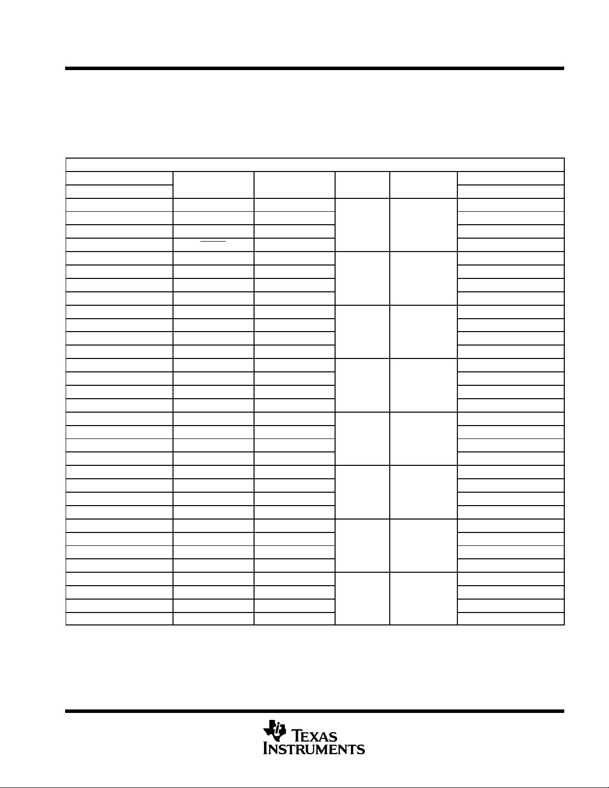
AVAILABLE OPTIONS
PACKAGED DEVICES
(PZ)
MSP430FG4616IPZ MSP430FG4616IZQW
MSP430FG4617IPZ MSP430FG4617IZQW
MSP430FG4618IPZ MSP430FG4618IZQW
MSP430FG4619IPZ MSP430FG4619IZQW
MSP430CG4616IPZ MSP430CG4616IZQW
MSP430CG4617IPZ MSP430CG4617IZQW
MSP430CG4618IPZ MSP430CG4618IZQW
MSP430CG4619IPZ MSP430CG4619IZQW
PLASTIC 113-BALL BGA
(ZQW)
2
POST OFFICE BOX 655303 • DALLAS, TEXAS 75265
Page 3
pin designation, MSP430xG461xIPZ
SS1
CCAVSS
P6.1/A1/OA0O
P6.2/A2/OA0I1
AV
96
97
98
30
29
28
DV
P6.3/A3/OA1O
P6.4/A4/OA1I0
P6.5/A5/OA2O
P6.6/A6/DAC0/OA2I0
P6.7/A7/DAC1/SVSIN
VeREF+/DAC0
VREF--/VeREF--
P5.1/S0/A12/DAC1
P5.0/S1/A13/OA1I1
P10.7/S2/A14/OA2I1
P10.6/S3/A15
CC1
VREF+
XIN
XOUT
P10.5/S4
P10.4/S5
P10.3/S6
P10.2/S7
P10.1/S8
P10.0/S9
P9.7/S10
P9.6/S11
P9.5/S12
P9.4/S13
1
2
3
4
5
6
7
8
9
10
11
12
13
14
15
16
17
18
19
20
21
22
23
24
25
100
26
DV
99
27
P6.0/A0/OA0I0
RST/NMI
TCK
TMS
92
93
94
95
MSP430xG4616IPZ
MSP430xG4617IPZ
MSP430xG4618IPZ
MSP430xG4619IPZ
34
33
32
31
XT2IN
TDI/TCLK
TDO/TDI
89
90
91
37
36
35
XT2OUT
88
38
P1.0/TA0
P1.1/TA0/MCLK
86
87
40
39
MIXED SIGNAL MICROCONTROLLER
P1.3/TBOUTH/SVSOUT
P1.4/TBCLK/SMCLK
84
42
83
43
P1.5/TACLK/ACLK
82
44
P1.2/TA1
85
41
MSP430xG461x
SLAS508G -- APRIL 2006 -- REVISED OCTOBER 2007
P1.7/CA1
P1.6/CA0
P2.0/TA2
79
80
81
47
46
45
P2.3/TB2
P2.1/TB0
P2.2/TB1
76
77
78
50
49
48
75
P2.4/UCA0TXD
74
P2.5/UCA0RXD
73
P2.6/CAOUT
72
P2.7/ADC12CLK/DMAE0
71
P3.0/UCB0STE
70
P3.1/UCB0SIMO/UCB0SDA
69
P3.2/UCB0SOMI/UCB0SCL
P3.3/UCB0CLK
68
P3.4/TB3
67
P3.5/TB4
66
P3.6/TB5
65
P3.7/TB6
64
P4.0/UTXD1
63
P4.1/URXD1
62
DV
61
60
59
58
57
56
55
54
53
52
51
SS2
DV
CC2
LCDCAP/R33
P5.7/R23
P5.6/LCDREF/R13
P5.5/R03
P5.4/COM3
P5.3/COM2
P5.2/COM1
COM0
P4.2/STE1/S39
P9,2/S15
P9.1/S16
P9.3/S14
P9.0/S17
P8.6/S19
P8.7/S18
P8.5/S20
P8.4/S21
P8.3/S22
POST OFFICE BOX 655303 • DALLAS, TEXAS 75265
P8.0/S25
P8.1/S24
P8.2/S23
P7.7/S26
P7.6/S27
P7.5/S28
P7.4/S29
P7.3/UCA0CLK/S30
P7.2/UCA0SOMI/S31
P4.4/SOMI1/S37
P4.3/SIMO1/S38
P4.5/UCLK1/S36
P7.0/UCA0STE/S33
P4.6/UCA0TXD/S35
P4.7/UCA0RXD/S34
P7.1/UCA0SIMO/S32
3
Page 4
MSP430xG461x
MIXED SIGNAL MICROCONTROLLER
SLAS508G -- APRIL 2006 -- REVISED OCTOBER 2007
pin designation, MSP430xG461xIZQW (top view)
A
B
C
D
E
F
G
H
J
K
L
M
12345 6789101112
NOTE: For terminal assignments, see the MSP430xG461x Terminal Functions table.
4
POST OFFICE BOX 655303 • DALLAS, TEXAS 75265
Page 5
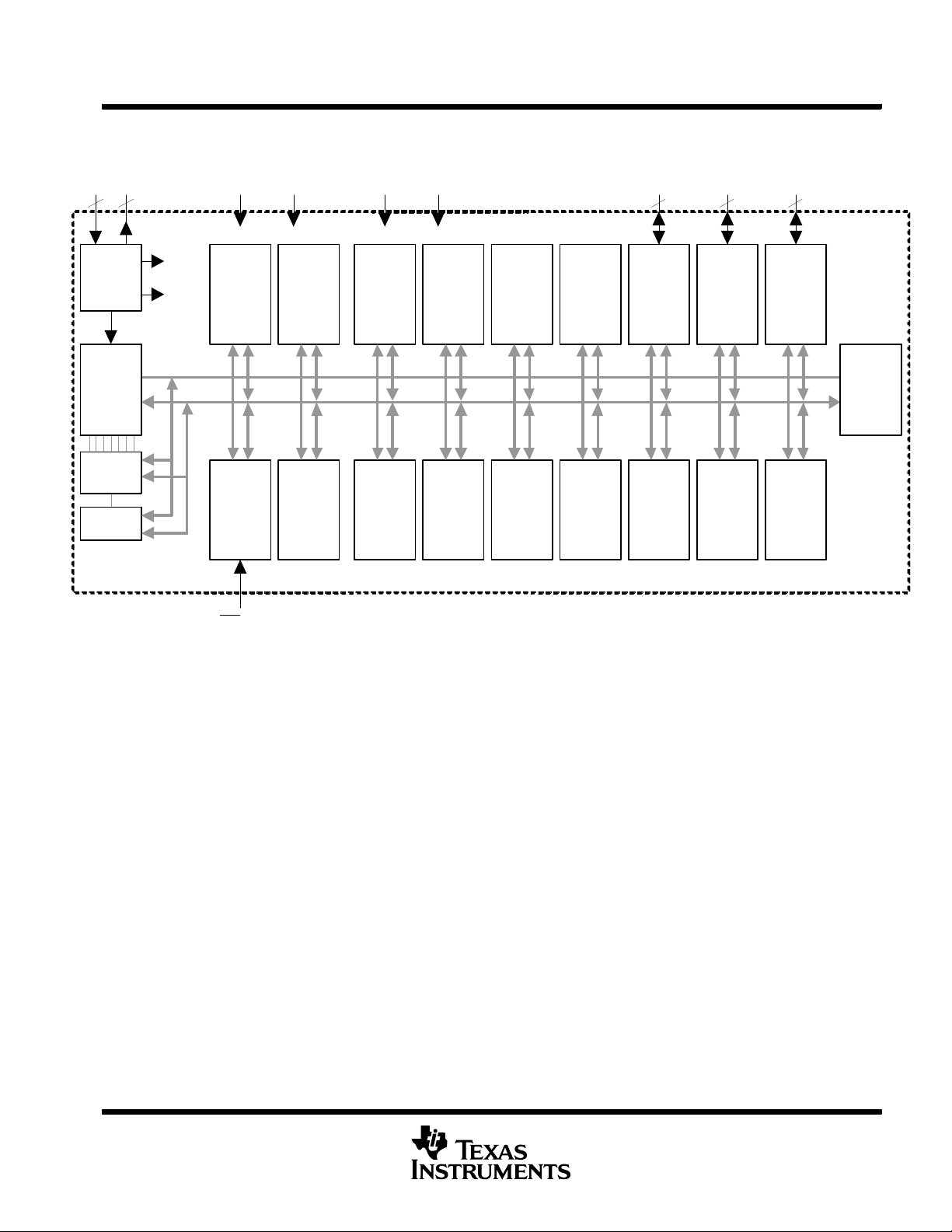
functional block diagram
MSP430xG461x
MIXED SIGNAL MICROCONTROLLER
SLAS508G -- APRIL 2006 -- REVISED OCTOBER 2007
XIN/
XT2IN
Oscillators
FLL+
8MH z
CPUX
incl. 16
Registers
Enhanced
Emulation
(FG only)
JTAG
Interface
XOUT/
XT2OUT
22
MCLK
ACLK
SMCLK
DVCC1/2 DVSS1/2
Flash(FG)
ROM(CG)
120kB
116k B
92kB
92kB
MAB
MDB
Brownout
Protection
SVS/ SVM
RST/NMI
RAM
4kB
8kB
8kB
4kB
Hardware
Multiplier
MPY,
MPYS,
MAC,
MACS
AVC C AVSS P1.x/P2.x
ADC12
12--Bit
12
Channels
Watchdog
WDT+
15/16--Bit
DAC12
12--Bit
2 Channels
Voltage out
Timer _A3
3CC
Registers
OA0, OA1,
OA2
3OpAmps
Timer_B7
7CC
Registers,
Shadow
Reg
Comparator
_A
Basic Timer
Real--Time
Clock
Ports P1/P2
2x8 I/O
Interrupt
capability
LCD_A
&
Segments
1, 2, 3 ,4 Mux
160
2x8
P3 .x/P4.x
P5 .x/P6.x
Ports
P3/P4
P5/P6
4x8 I/O
USCI_A0:
UART,
IrDA, SPI
USCI_B0:
SPI, I2C
4x8
P7.x/P8.x
P9.x/P 10.x
4x8/2x16
Ports
P7/ P8
P9/P10
4x8 / 2x16 I/O
USART1
UART, SPI
DMA
Controller
3 Channels
POST OFFICE BOX 655303 • DALLAS, TEXAS 75265
5
Page 6
MSP430xG461x
MIXED SIGNAL MICROCONTROLLER
SLAS508G -- APRIL 2006 -- REVISED OCTOBER 2007
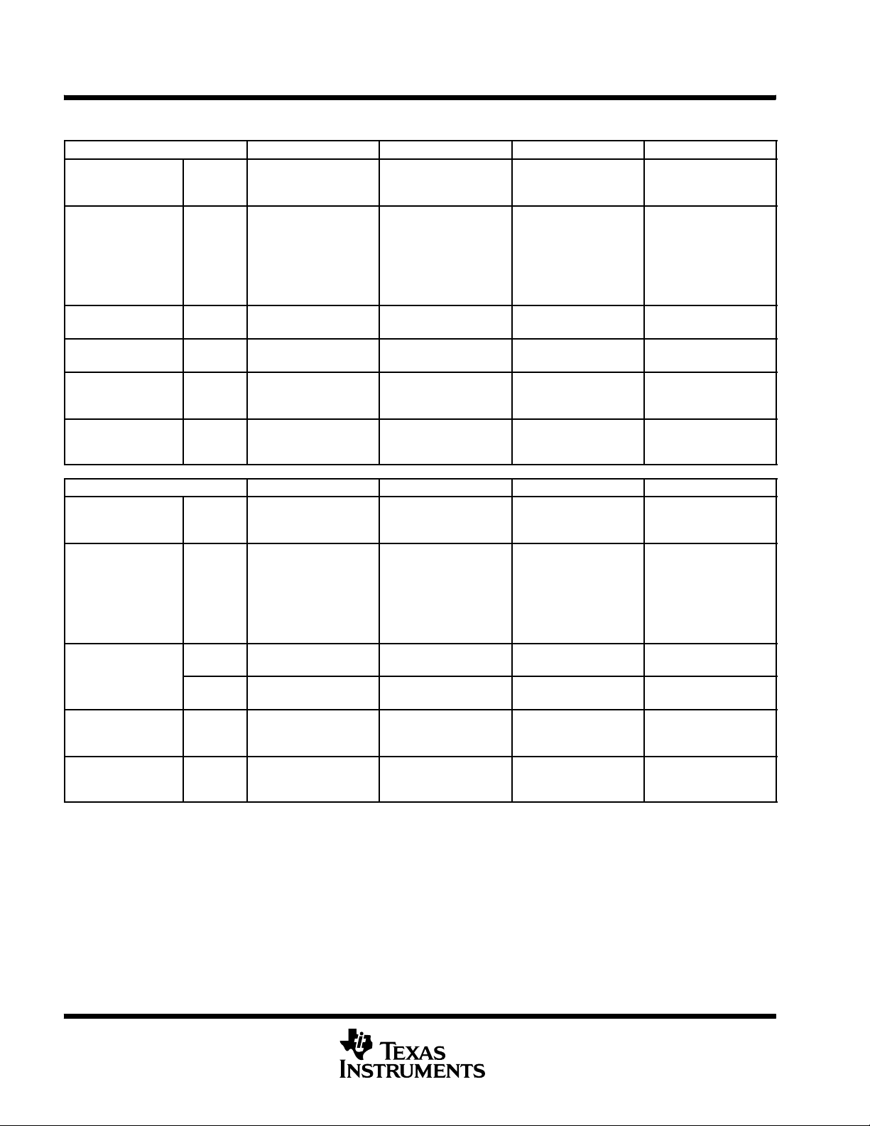
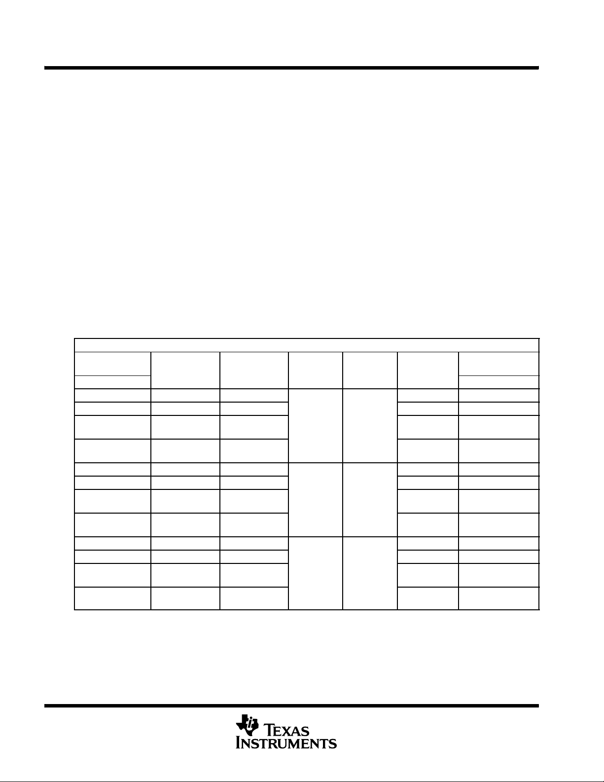
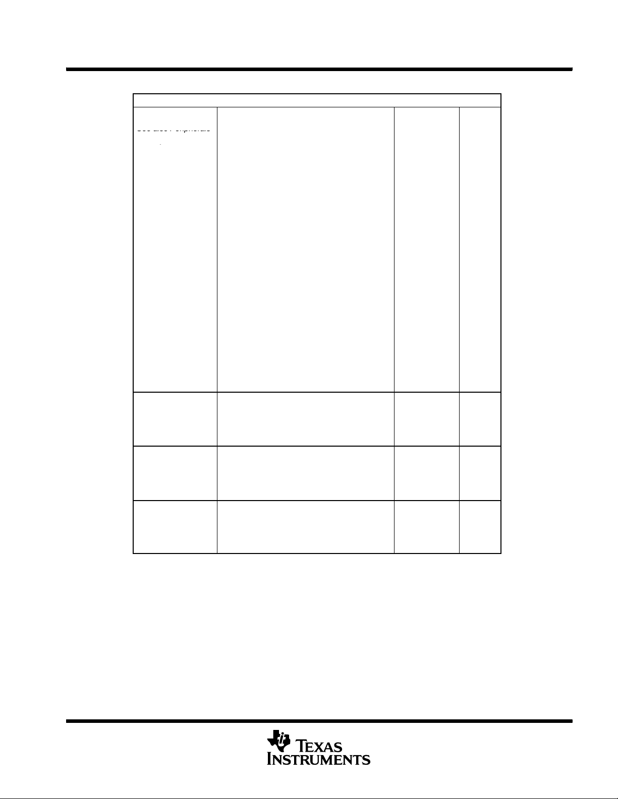
Terminal Functions
TERMINAL
NAME
DV
CC1
P6.3/A3/OA1O 2 B1 I/O General-purpose digital I/O / analog input a3—12-bit ADC / OA1 output
P6.4/A4/OA1I0 3
P6.5/A5/OA2O 4 C2 I/O General-purpose digital I/O / analog input a5—12-bit ADC / OA2 output
P6.6/A6/DAC0/OA2I0 5
P6.7/A7/DAC1/SVSIN 6 C3 I/O
V
REF+
XIN 8 D1 I Input port for crystal oscillator XT1. Standard or watch crystals can be connected.
XOUT 9 E1 O Output terminal of crystal oscillator XT1
Ve
/DAC0 10 E2 I/O Input for an external reference voltage to the ADC / DAC12.0 output
REF+
V
/Ve
REF--
REF--
P5.1/S0/A12/DAC1 (see Note 1) 12 F1 I/O
P5.0/S1/A13/OA1I1 (see Note 1) 13 F2 I/O
P10.7/S2/A14/OA2I1 (see Note 1) 14 E5 I/O
P10.6/S3/A15 (see Note 1) 15 G1 I/O
P10.5/S4 16 G2 I/O General-purpose digital I/O / LCD segment output 4
P10.4/S5 17 F4 I/O General-purpose digital I/O / LCD segment output 5
P10.3/S6 18 H1 I/O General-purpose digital I/O / LCD segment output 6
P10.2/S7 19 H2 I/O General-purpose digital I/O / LCD segment output 7
P10.1/S8 20 F5 I/O General-purpose digital I/O / LCD segment output 8
P10.0/S9 21 J1 I/O General-purpose digital I/O / LCD segment output 9
P9.7/S10 22 J2 I/O General-purpose digital I/O / LCD segment output 10
P9.6/S11 23 G4 I/O General-purpose digital I/O / LCD segment output 11
P9.5/S12 24 K1 I/O General-purpose digital I/O / LCD segment output 12
P9.4/S13 25 L1 I/O General-purpose digital I/O / LCD segment output 13
P9.3/S14 26 M2 I/O General-purpose digital I/O / LCD segment output 14
P9.2/S15 27 K2 I/O General-purpose digital I/O / LCD segment output 15
P9.1/S16 28 L3 I/O General-purpose digital I/O / LCD segment output 16
P9.0/S17 29 M3 I/O General-purpose digital I/O / LCD segment output 17
P8.7/S18 30 H4 I/O General-purpose digital I/O / LCD segment output 18
P8.6/S19 31 L4 I/O General-purpose digital I/O / LCD segment output 19
P8.5/S20 32 M4 I/O General-purpose digital I/O / LCD segment output 20
P8.4/S21 33 G5 I/O General-purpose digital I/O / LCD segment output 21
P8.3/S22 34 L5 I/O General-purpose digital I/O / LCD segment output 22
NOTES: 1. Segments S0 through S3 are disabled when the LCD charge pump feature is enabled (LCDCPEN = 1) and cannot be used together
with the LCD charge pump. In addition, when using segments S0 through S3 with an external LCD voltage supply, V
NO.PZNO.
ZQW
1 A1 Digital supply voltage, positive terminal
7 D2 O Output of positive terminal of the reference voltage in the ADC
11 E4 I
I/O DESCRIPTION
I/O General-purpose digital I/O / analog input a4—12-bit ADC / OA1 input multiplexer
B2
C1
on +terminal and -- terminal
I/O General-purpose digital I/O / analog input a6—12-bit ADC / DAC12.0 output / OA2
input multiplexer on +terminal and --terminal
General-purpose digital I/O / analog input a7—12-bit ADC / DAC12.1 output /
analog input to brownout, supply voltage supervisor
Negative terminal for the ADC reference voltage for both sources, the internal
reference voltage, or an external applied reference voltage
General-purpose digital I/O / LCD segment output 0 / analog input a12 -- 12--bit
ADC / DAC12.1 output
General-purpose digital I/O / LCD segment output 1 / analog input a13 -- 12--bit
ADC/OA1 input multiplexer on +terminal and --terminal
General-purpose digital I/O / LCD segment output 2 / analog input a14 -- 12--bit
ADC/OA2 input multiplexer on +terminal and --terminal
General-purpose digital I/O / LCD segment output 3 / analog input a15 -- 12--bit
ADC
LCD
≤ AVCC.
6
POST OFFICE BOX 655303 • DALLAS, TEXAS 75265
Page 7

MSP430xG461x
MIXED SIGNAL MICROCONTROLLER
SLAS508G -- APRIL 2006 -- REVISED OCTOBER 2007
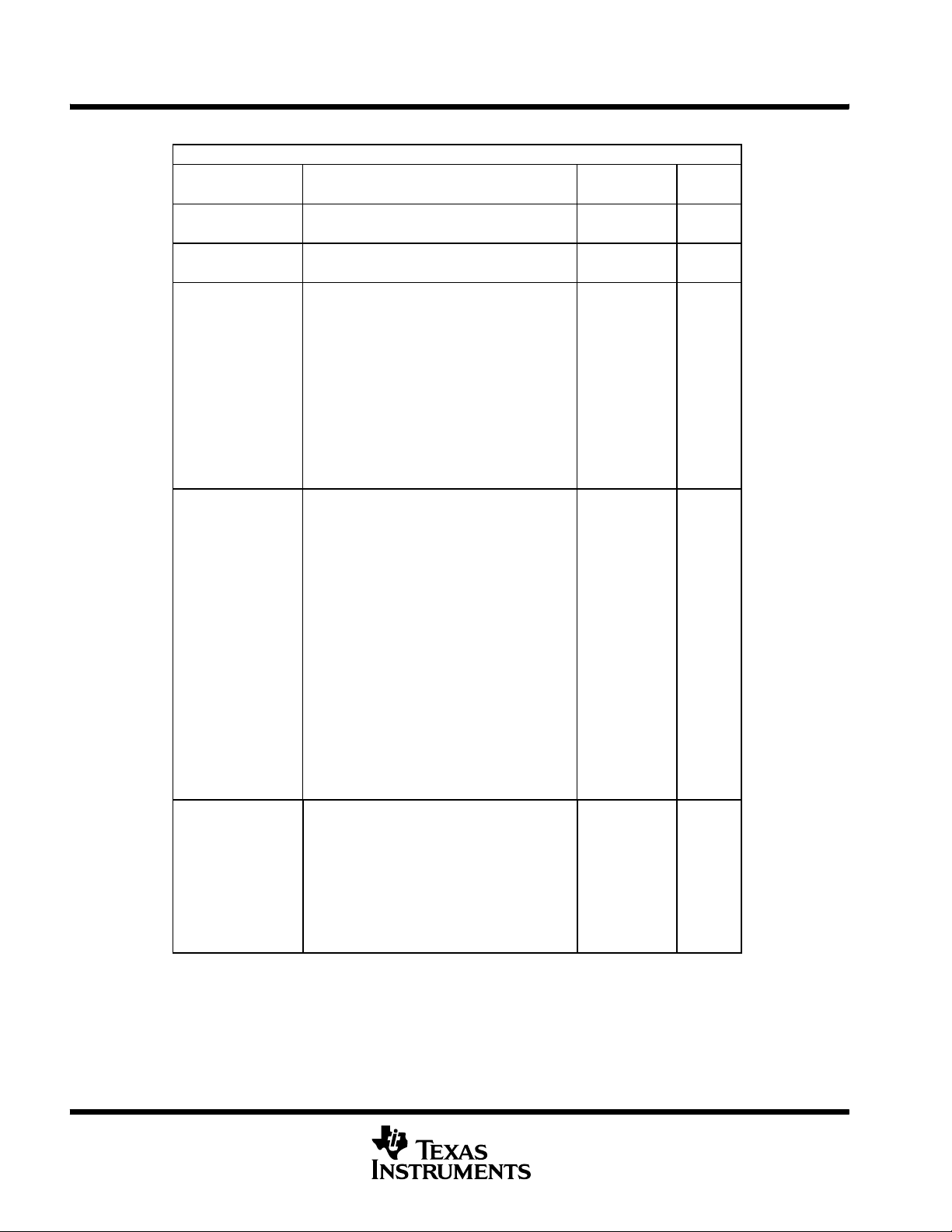
Terminal Functions (Continued)
TERMINAL
NAME
P8.2/S23 35 M5 I/O General-purpose digital I/O / LCD segment output 23
P8.1/S24 36 H5 I/O General-purpose digital I/O / LCD segment output 24
P8.0/S25 37 J5 I/O General-purpose digital I/O / LCD segment output 25
P7.7/S26 38 M6 I/O General-purpose digital I/O / LCD segment output 26
P7.6/S27 39 L6 I/O General-purpose digital I/O / LCD segment output 27
P7.5/S28 40 J6 I/O General-purpose digital I/O / LCD segment output 28
P7.4/S29 41 M7 I/O General-purpose digital I/O / LCD segment output 29
P7.3/UCA0CLK/S30 42 H6 I/O
P7.2/UCA0SOMI/S31 43 L7 I/O
P7.1/UCA0SIMO/S32 44 M8 I/O
P7.0/UCA0STE/S33 45 L8 I/O
P4.7/UCA0RXD/S34 46 J7 I/O
P4.6/UCA0TXD/S35 47 M9 I/O
P4.5/UCLK1/S36 48 L9 I/O
P4.4/SOMI1/S37 49 H7 I/O
P4.3/SIMO1/S38 50 M10 I/O
P4.2/STE1/S39 51 M11 I/O
COM0 52 L10 O COM0--3 are used for LCD backplanes.
P5.2/COM1 53 L12 I/O General-purpose digital I/O / common output, COM0--3 are used for LCD backplanes.
P5.3/COM2 54 J8 I/O General-purpose digital I/O / common output, COM0--3 are used for LCD backplanes.
P5.4/COM3 55 K12 I/O General-purpose digital I/O / common output, COM0--3 are used for LCD backplanes.
P5.5/R03 56 K11 I/O General-purpose digital I/O / Input port of lowest analog LCD level (V5)
P5.6/LCDREF/R13 57 J12 I/O
P5.7/R23 58 J11 I/O General-purpose digital I/O / Input port of second most positive analog LCD level (V2)
LCDCAP/R33 59 H11 I LCD capacitor connection / Input/output port of most positive analog LCD level (V1)
DV
CC2
DV
SS2
P4.1/URXD1 62 G1 1 I/O General-purpose digital I/O / receive data in—USART1/UART mode
P4.0/UTXD1 63 H9 I/O General-purpose digital I/O / transmit data out—USART1/UART mode
P3.7/TB6 64 F12 I/O
P3.6/TB5 65 F11 I/O
P3.5/TB4 66 G9 I/O
NO.PZNO.
ZQW
60 H12 Digital supply voltage, positive terminal
61 G12 Digital supply voltage, negative terminal
I/O DESCRIPTION
General-purpose digital I/O / external clock input -- USCI_A0/UART or SPI mode, clock
output -- USCI_A0/SPI mode / LCD segment 30
General-purpose digital I/O / slave out/master in of USCI_A0/SPI mode / LCD segment
output 31
General-purpose digital I/O / slave in/master out of USCI_A0/SPI mode / LCD segment
output 32
General-purpose digital I/O / slave transmit enable—USCI_A0/SPI mode / LCD segment
output 33
General-purpose digital I/O / receive data in -- USCI_A0/UART or IrDA mode / LCD
segment output 34
General-purpose digital I/O / transmit data out -- USCI_A0/UART or IrDA mode / LCD
segment output 35
General-purpose digital I/O / external clock input -- USART1/UART or SPI mode,
clock output -- USART1/SPI MODE / LCD segment output 36
General-purpose digital I/O / slave out/master in of USART1/SPI mode / LCD segment
output 37
General-purpose digital I/O / slave in/master out of USART1/SPI mode / LCD segment
output 38
General-purpose digital I/O / slave transmit enable—USART1/SPI mode / LCD segment
output 39
General-purpose digital I/O / External reference voltage input for regulated LCD voltage
/ Input port of third most positive analog LCD level (V4 or V3)
General-purpose digital I/O / Timer_B7 CCR6. Capture: CCI6A/CCI6B input, compare:
Out6 output
General-purpose digital I/O / Timer_B7 CCR5. Capture: CCI5A/CCI5B input, compare:
Out5 output
General-purpose digital I/O / Timer_B7 CCR4. Capture: CCI4A/CCI4B input, compare:
Out4 output
POST OFFICE BOX 655303 • DALLAS, TEXAS 75265
7
Page 8
MSP430xG461x
MIXED SIGNAL MICROCONTROLLER
SLAS508G -- APRIL 2006 -- REVISED OCTOBER 2007
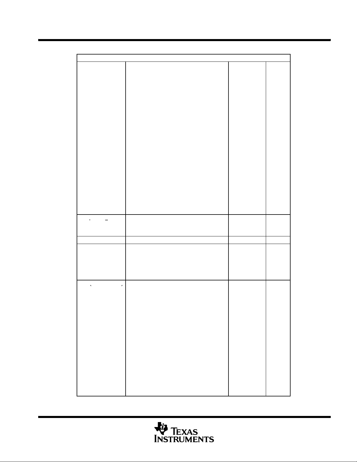
Terminal Functions (Continued)
TERMINAL
NAME
P3.4/TB3 67 E12 I/O
P3.3/UCB0CLK 68 E11 I/O
P3.2/UCB0SOMI/
UCB0SCL
P3.1/UCB0SIMO/
UCB0SDA
P3.0/UCB0STE 71 D11 I/O General-purpose digital I/O / slave transmit enable—USCI_B0/SPI mode
P2.7/ADC12CLK/
DMAE0
P2.6/CAOUT 73 C12 I/O General -purpose digital I/O / Comparator_A output
P2.5/UCA0RXD 74 C11 I/O General-purpose digital I/O / receive data in—USCI_A0/UART or IrDA mode
P2.4/UCA0TXD 75 B12 I/O General-purpose digital I/O / transmit data out—USCI_A0/UART or IrDA mode
P2.3/TB2 76 A11 I/O
P2.2/TB1 77 E8 I/O
P2.1/TB0 78 D8 I/O
P2.0/TA2 79 A10 I/O General-purpose digital I/O / Timer_A Capture: CCI2A input, compare: Out2 output
P1.7/CA1 80 B10 I/O General-purpose digital I/O / Comparator_A input
P1.6/CA0 81 A9 I/O General-purpose digital I/O / Comparator_A input
P1.5/TACLK/ACLK 82 B9 I/O
P1.4/TBCLK/SMCLK 83 B8 I/O
P1.3/TBOUTH/SVSOUT 84 A8 I/O
P1.2/TA1 85 D7 I/O General-purpose digital I/O / Timer_A, Capture: CCI1A input, compare: Out1 output
P1.1/TA0/MCLK 86 E7 I/O
P1.0/TA0 87 A7 I/O
XT2OUT 88 B7 O Output terminal of crystal oscillator XT2
XT2IN 89 B6 I Input port for crystal oscillator XT2. Only standard crystals can be connected.
TDO/TDI 90 A6 I/O Test data output port. TDO/TDI data output or programming data input terminal
TDI/TCLK 91 D6 I Test data input or test clock input. The device protection fuse is connected to TDI/TCLK.
TMS 92 E6 I Test mode select. TMS is used as an input port for device programming and test.
TCK 93 A5 I Test clock. TCK is the clock input port for device programming and test.
RST/NMI 94 B5 I Reset input or nonmaskable interrupt input port
P6.0/A0/OA0I0 95 A4 I/O
P6.1/A1/OA0O 96 D5 I/O General-purpose digital I/O / analog input a1—12-bit ADC / OA0 output
P6.2/A2/OA0I1 97 B4 I/O
NO.PZNO.
ZQW
69 F9 I/O
70 D12 I/O
72 E9 I/O General-purpose digital I/O / conversion clock—12-bit ADC / DMA Channel 0 external trigger
I/O DESCRIPTION
General-purpose digital I/O / Timer_B7 CCR3. Capture: CCI3A/CCI3B input, compare: Out3
output
General-purpose digital I/O / external clock input—USCI_B0/UART or SPI mode, clock
output—USCI_B0/SPI mode
General-purpose digital I/O / slave out/master in of USCI_B0/SPI mode /I2C
clock—USCI_B0/I2C mode
General-purpose digital I/O / slave in/master out of USCI_B0/SPI mode, I2C
data—USCI_B0/I2C mode
General-purpose digital I/O / Timer_B7 CCR2. Capture: CCI2A/CCI2B input, compare: Out2
output
General-purpose digital I/O / Timer_B7 CCR1. Capture: CCI1A/CCI1B input, compare: Out1
output
General-purpose digital I/O / Timer_B7 CCR0. Capture: CCI0A/CCI0B input, compare: Out0
output
General-purpose digital I/O / Timer_A, clock signal TACLK input / ACLK output (divided by
1, 2, 4, or 8)
General-purpose digital I/O / input clock TBCLK—Timer_B7 / submain system clock SMCLK
output
General-purpose digital I/O / switch all PWM digital output ports to high
impedance—Timer_B7 TB0 to TB6 / SVS: output of SVS comparator
General-purpose digital I/O / Timer_A. Capture: CCI0B input / MCLK output.
Note: TA0 is only an input on this pin / BSL receive
General-purpose digital I/O / Timer_A. Capture: CCI0A input, compare: Out0 output / BSL
transmit
General-purpose digital I/O / analog input a0—12-bit ADC / OA0 input multiplexer on
+ terminal and -- terminal
General-purpose digital I/O / analog input a2—12-bit ADC / OA0 input multiplexer on
+ terminal and -- terminal
8
POST OFFICE BOX 655303 • DALLAS, TEXAS 75265
Page 9
MSP430xG461x
MIXED SIGNAL MICROCONTROLLER
SLAS508G -- APRIL 2006 -- REVISED OCTOBER 2007
Terminal Functions (Continued)
TERMINAL
NAME
AV
SS
DV
(see Note 1) 99 B3 Digital supply voltage, negative terminal
SS1
AV
CC
NOTE 1: All unassigned ball locations on the ZQW package should be electrically tied to the ground supply. The shortest ground return path to
the device should be established via ball location B3.
NO.PZNO.
ZQW
98 A3
100 A2
I/O DESCRIPTION
Analog supply voltage, negative terminal. Supplies SVS, brownout, oscillator,comparator_A,
port 1
Analog supply voltage, positive terminal. Supplies SVS, brownout, oscillator, comparator_A,
port 1; must not power up prior to DV
CC1
/DV
CC2
.
POST OFFICE BOX 655303 • DALLAS, TEXAS 75265
9
Page 10
MSP430xG461x
MIXED SIGNAL MICROCONTROLLER
SLAS508G -- APRIL 2006 -- REVISED OCTOBER 2007
short-form description
CPU
The MSP430 CPU has a 16-bit RISC architecture
that is highly transparent to the application. All
operations, other than program-flow instructions,
are performed as register operations in
conjunction with seven addressing modes for
source operand and four addressing modes for
destination operand.
The CPU is integrated with 16 registers that
provide reduced instruction execution time. The
register-to-register operation execution time is
one cycle of the CPU clock.
Four of the registers, R0 to R3, are dedicated as
program counter, stack pointer, status register,
and constant generator respectively. The
remaining registers are general-purpose
registers.
Peripherals are connected to the CPU using data,
address, and control buses, and can be handled
with all instructions.
The MSP430xG461x device family utilizes the
MSP430X CPU and is completely backwards
compatible with the MSP430 CPU. For a complete
description of the MSP430X CPU, refer to the
MSP430x4xx Family User’s Guide.
instruction set
The instruction set consists of the original 51
instructions with three formats and seven address
modes and additional instructions for the
expanded address range. Each instruction can
operate on word and byte data. Table 1 shows
examples of the three types of instruction formats;
the address modes are listed in Table 2.
Program Counter
Stack Pointer
Status Register
Constant Generator
General-Purpose Register
General-Purpose Register
General-Purpose Register
General-Purpose Register
General-Purpose Register
General-Purpose Register
General-Purpose Register
General-Purpose Register
General-Purpose Register
General-Purpose Register
General-Purpose Register
General-Purpose Register
PC/R0
SP/R1
SR/CG1/R2
CG2/R3
R4
R5
R6
R7
R8
R9
R10
R11
R12
R13
R14
R15
10
POST OFFICE BOX 655303 • DALLAS, TEXAS 75265
Page 11
MSP430xG461x
MIXED SIGNAL MICROCONTROLLER
SLAS508G -- APRIL 2006 -- REVISED OCTOBER 2007
Table 1. Instruction Word Formats
Dual operands, source-destination e.g., ADD R4,R5 R4 + R5 ------> R5
Single operands, destination only e.g., CALL R8 PC ---->(TOS), R8----> PC
Relative jump, un/conditional e.g., JNE Jump-on-equal bit = 0
Table 2. Address Mode Descriptions
ADDRESS MODE S D SYNTAX EXAMPLE OPERATION
Register F
Indexed F F MOV X(Rn),Y(Rm) MOV 2(R5),6(R6) M(2+R5)—> M(6+R6)
Symbolic (PC relative) F F MOV EDE,TONI M(EDE) —> M(TONI)
Absolute F F MOV&MEM,&TCDAT M(MEM) —> M(TCDAT)
Indirect F MOV @Rn,Y(Rm) MOV @R10,Tab(R6) M(R10) —> M(Tab+R6)
Indirect
autoincrement
Immediate F MOV #X,TONI MOV #45,TONI #45 —> M(TONI)
NOTE: S = source D = destination
F
F MOV @Rn+,Rm MOV @R10+,R11
MOV Rs,Rd MOV R10,R11 R10 —> R11
M(R10) —> R11
R10 + 2—> R10
POST OFFICE BOX 655303 • DALLAS, TEXAS 75265
11
Page 12

MSP430xG461x
MIXED SIGNAL MICROCONTROLLER
SLAS508G -- APRIL 2006 -- REVISED OCTOBER 2007
operating modes
The MSP430 has one active mode and five software-selectable low-power modes of operation. An interrupt
event can wake up the device from any of the five low-power modes, service the request, and restore back to
the low-power mode on return from the interrupt program.
The following six operating modes can be configured by software:
D Active mode (AM)
-- All clocks are active
D Low-power mode 0 (LPM0)
-- CPU is disabled
ACLK and SMCLK remain active. MCLK is disabled
FLL+ loop control remains active
D Low-power mode 1 (LPM1)
-- CPU is disabled
FLL+ loop control is disabled
ACLK and SMCLK remain active. MCLK is disabled
D Low-power mode 2 (LPM2)
-- CPU is disabled
MCLK, FLL+ loop control and DCOCLK are disabled
DCO’s dc-generator remains enabled
ACLK remains active
D Low-power mode 3 (LPM3)
-- CPU is disabled
MCLK, FLL+ loop control, and DCOCLK are disabled
DCO’s dc-generator is disabled
ACLK remains active
D Low-power mode 4 (LPM4)
-- CPU is disabled
ACLK is disabled
MCLK, FLL+ loop control, and DCOCLK are disabled
DCO’s dc-generator is disabled
Crystal oscillator is stopped
12
POST OFFICE BOX 655303 • DALLAS, TEXAS 75265
Page 13
MSP430xG461x
ReservedReserved(seeNote4
)
MIXED SIGNAL MICROCONTROLLER
SLAS508G -- APRIL 2006 -- REVISED OCTOBER 2007
interrupt vector addresses
The interrupt vectors and the power-up start address are located in the address range 0FFFFh to 0FFC0h. The
vector contains the 16-bit address of the appropriate interrupt-handler instruction sequence.
Table 3. Interrupt Sources, Flags, and Vectors of MSP430xG461x Configurations
INTERRUPT SOURCE INTERRUPT FLAG SYSTEM INTERRUPT
Power-Up
External Reset
Watchdog
Flash Memory
NMI
Oscillator Fault
Flash Memory Access Violation
Timer_B7 TBCCR0 CCIFG0 (see Note 2) Maskable 0FFFAh 29
Timer_B7
Comparator_A CAIFG Maskable 0FFF6h 27
Watchdog Timer+ WDTIFG Maskable 0FFF4h 26
USCI_A0/USCI_B0 Receive UCA0RXIFG, UCB0RXIFG (see Note 1) Maskable 0FFF2h 25
USCI_A0/USCI_B0 Transmit UCA0TXIFG, UCB0TXIFG (see Note 1) Maskable 0FFF0h 24
ADC12 ADC12IFG (see Notes 1 and 2) Maskable 0FFEEh 23
Timer_A3 TACCR0 CCIFG0 (see Note 2) Maskable 0FFECh 22
Timer_A3
I/O Port P1 (Eight Flags) P1IFG.0 to P1IFG.7 (see Notes 1 and 2) Maskable 0FFE8h 20
USART1 Receive URXIFG1 Maskable 0FFE6h 19
USART1 Transmit UTXIFG1 Maskable 0FFE4h 18
I/O Port P2 (Eight Flags) P2IFG.0 to P2IFG.7 (see Notes 1 and 2) Maskable 0FFE2h 17
Basic Timer1/RTC BTIFG Maskable 0FFE0h 16
DMA DMA0IFG, DMA1IFG, DMA2IFG
DAC12 DAC12.0IFG, DAC12.1IFG (see Notes 1 and 2) Maskable 0FFDCh 14
Reserved Reserved (see Note 4)
NOTES: 1. Multiple source flags
2. Interrupt flags are located in the module.
3. A reset is generated if the CPU tries to fetch instructions from within the module register memory address range (0h to 01FFh).
(Non)maskable: the individual interrupt -enable bit can disable an interrupt event, but the general-interrupt enable cannot disable it.
4. The interrupt vectors at addresses 0FFDAh to 0FFC0h are not used in this device and can be used for regular program code if
necessary.
5. Access and key violations, KEYV and ACCVIFG, only applicable to F devices.
NMIIFG (see Notes 1 and 3)
OFIFG (see Notes 1 and 3)
ACCVIFG (see Notes 1, 2, and 5)
TBCCR1 CCIFG1 ... TBCCR6 CCIFG6,
TBIFG (see Notes 1 and 2)
TACCR1 CCIFG1 and TACCR2 CCIFG2,
TAIFG (see Notes 1 and 2)
WDTIFG
KEYV
(see Note 1 and 5)
(see Notes 1 and 2)
Reset 0FFFEh 31, highest
(Non)maskable
(Non)maskable
(Non)maskable
Maskable 0FFF8h 28
Maskable 0FFEAh 21
Maskable 0FFDEh 15
WORD
ADDRESS
0FFFCh 30
0FFDAh 13
... ...
0FFC0h 0, lowest
PRIORITY
POST OFFICE BOX 655303 • DALLAS, TEXAS 75265
13
Page 14
MSP430xG461x
MIXED SIGNAL MICROCONTROLLER
SLAS508G -- APRIL 2006 -- REVISED OCTOBER 2007
special function registers (SFRs)
The MSP430 SFRs are located in the lowest address space and are organized as byte mode registers. SFRs
should be accessed with byte instructions.
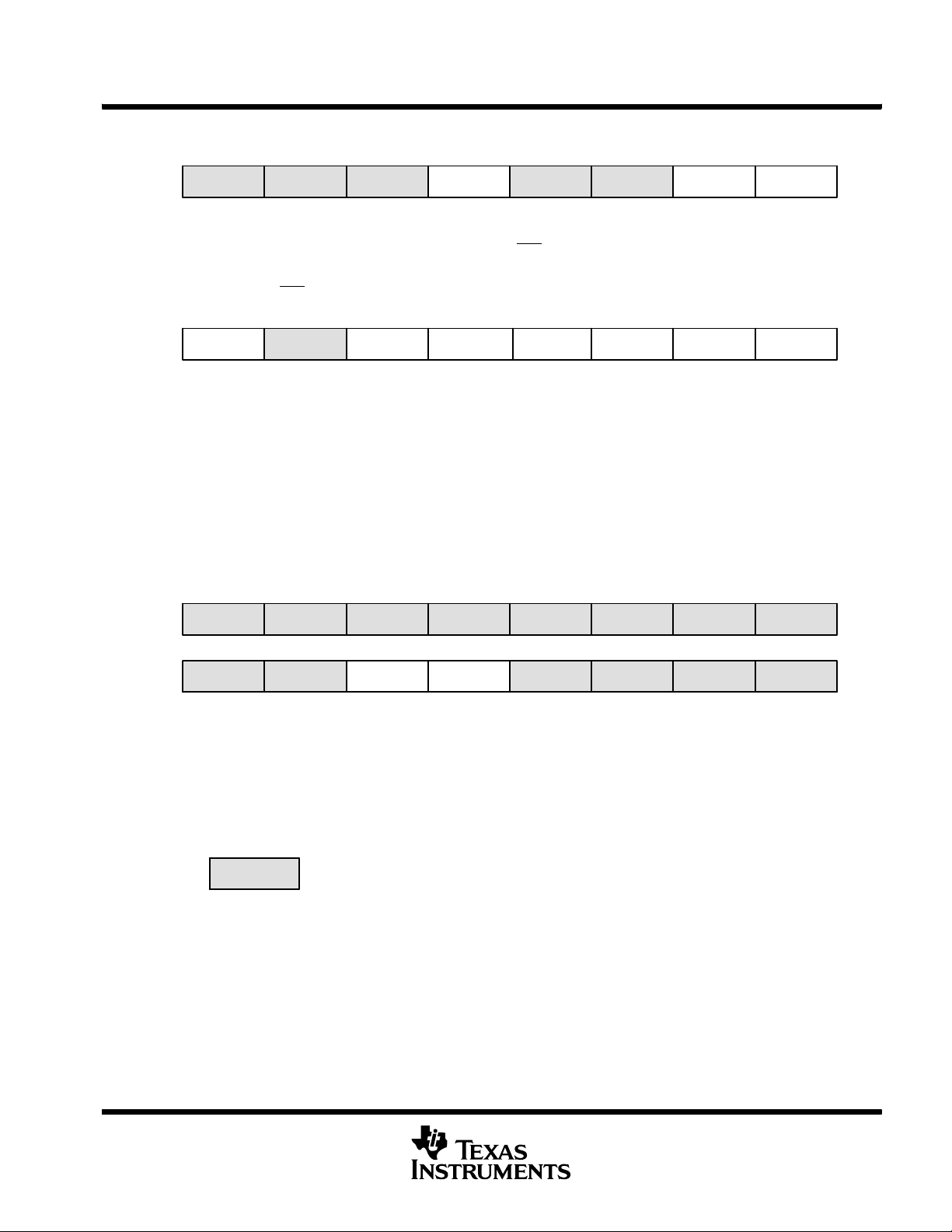
interrupt enable 1 and 2
Address
0h ACCVIE NMIIE
WDTIE Watchdog-timer interrupt enable. Inactive if watchdog mode is selected.
OFIE Oscillator-fault-interrupt enable
NMIIE Nonmaskable-interrupt enable
ACCVIE Flash access violation interrupt enable
Address
01h
UCA0RXIE USCI_A0 receive-interrupt enable
UCA0TXIE USCI_A0 transmit-interrupt enable
UCB0RXIE USCI_B0 receive-interrupt enable
UCB0TXIE USCI_B0 transmit-interrupt enable
URXIE1 USART1 UART and SPI receive-interrupt enable
UTXIE1 USART1 UART and SPI transmit-interrupt enable
BTIE Basic timer interrupt enable
7654 0
rw–0
Active if watchdog timer is configured as a general-purpose timer.
7654 032 1
BTIE UTXIE1 URXIE1
rw–0
rw–0 rw–0
rw–0 rw–0 rw–0
32 1
UCB0TXIE UCB0RXIE
rw–0 rw–0
OFIE WDTIE
UCA0TXIE UCA0RXIE
rw–0 rw–0
14
POST OFFICE BOX 655303 • DALLAS, TEXAS 75265
Page 15
interrupt flag register 1 and 2
MSP430xG461x
MIXED SIGNAL MICROCONTROLLER
SLAS508G -- APRIL 2006 -- REVISED OCTOBER 2007
Address
02h NMIIFG
WDTIFG: Set on watchdog timer overflow (in watchdog mode) or security key violation
OFIFG: Flag set on oscillator fault
NMIIFG: Set via RST
Address
03h
UCA0RXIFG USCI_A0 receive-interrupt flag
UCA0TXIFG USCI_A0 transmit-interrupt flag
UCB0RXIFG USCI_B0 receive-interrupt flag
UCB0TXIFG USCI_B0 transmit-interrupt flag
URXIFG0: USART1: UART and SPI receive flag
UTXIFG0: USART1: UART and SPI transmit flag
BTIFG: Basic timer flag
7654 0
rw–0 rw–1 rw–(0)
Reset on V
7654 032 1
BTIFG
rw–0
power-on or a reset condition at the RST/NMI pin in reset mode
CC
/NMI pin
UTXIFG1 URXIFG1
rw–1 rw–0
32 1
UCB0TXIFG UCB0RXIFG
rw–0 rw–0
module enable registers 1 and 2
Address
04h
7654 032 1
OFIFG WDTIFG
UCA0TXIFG UCA0RXIFG
rw–0 rw–0
Address
05h
URXE1: USART1: UART mode receive enable
UTXE1: USART1: UART mode transmit enable
USPIE1: USART1: SPI mode transmit and receive enable
Legend rw:
7654 0
rw-0,1:
rw-(0,1):
UTXE1
rw–0 rw–0
Bit can be read and written.
Bit can be read and written. It is Reset or Set by PUC.
Bit can be read and written. It is Reset or Set by POR.
SFR bit is not present in device
URXE1
USPIE1
32 1
POST OFFICE BOX 655303 • DALLAS, TEXAS 75265
15
Page 16
MSP430xG461x
MIXED SIGNAL MICROCONTROLLER
SLAS508G -- APRIL 2006 -- REVISED OCTOBER 2007
memory organization
MSP430FG4616 MSP430FG4617 MSP430FG4618 MSP430FG4619
Memory
Main: interrupt vector
Main: code memory
RAM (Total) Size 4KB
Extended Size 2KB
Mirrored Size 2KB
Information memory Size
Boot memory Size
RAM
(mirrored at
018FFh -- 01100h)
Peripherals 16 bit
Size
Flash
Flash
Flash
ROM
Size 2KB
8bit
8-bit SFR
018FFFh -- 002100h
92KB
0FFFFh -- 0FFC0h
020FFh -- 01100h
020FFh -- 01900h
018FFh -- 01100h
256 Byte
010FFh -- 01000h
1KB
0FFFh -- 0C00h
09FFh -- 0200h
01FFh -- 0100h
0FFh -- 010h
0Fh -- 00h
92KB
0FFFFh -- 0FFC0h
019FFFh -- 003100h
8KB
030FFh -- 01100h
6KB
030FFh -- 01900h
2KB
018FFh -- 01100h
256 Byte
010FFh -- 01000h
1KB
0FFFh -- 0C00h
2KB
09FFh -- 0200h
01FFh -- 0100h
0FFh -- 010h
0Fh -- 00h
116KB
0FFFFh -- 0FFC0h
01FFFFh -- 003100h
8KB
030FFh -- 01100h
6KB
030FFh -- 01900h
2KB
018FFh -- 01100h
256 Byte
010FFh -- 01000h
1KB
0FFFh -- 0C00h
2KB
09FFh -- 0200h
01FFh -- 0100h
0FFh -- 010h
0Fh -- 00h
120KB
0FFFFh -- 0FFC0h
01FFFFh -- 002100h
4KB
020FFh -- 01100h
2KB
020FFh -- 01900h
2KB
018FFh -- 01100h
256 Byte
010FFh -- 01000h
1KB
0FFFh -- 0C00h
2KB
09FFh -- 0200h
01FFh -- 0100h
0FFh -- 010h
0Fh -- 00h
MSP430CG4616 MSP430CG4617 MSP430CG4618 MSP430CG4619
Memory
Main: interrupt vector
Main: code memory
RAM (Total) Size 4KB
Extended Size 2KB
Mirrored Size 2KB
Information memory Size
Boot memory
(Optional on CG)
RAM
(mirrored at
018FFh -- 01100h)
Peripherals 16 bit
Size
ROM
ROM
ROM
Size
ROM
Size 2KB
8bit
8-bit SFR
018FFFh -- 002100h
92KB
0FFFFh -- 0FFC0h
020FFh -- 01100h
020FFh -- 01900h
018FFh -- 01100h
256 Byte
010FFh -- 01000h
1KB
0FFFh -- 0C00h
09FFh -- 0200h
01FFh -- 0100h
0FFh -- 010h
0Fh -- 00h
92KB
0FFFFh -- 0FFC0h
019FFFh -- 003100h
8KB
030FFh -- 01100h
6KB
030FFh -- 01900h
2KB
018FFh -- 01100h
256 Byte
010FFh -- 01000h
1KB
0FFFh -- 0C00h
2KB
09FFh -- 0200h
01FFh -- 0100h
0FFh -- 010h
0Fh -- 00h
116KB
0FFFFh -- 0FFC0h
01FFFFh -- 003100h
8KB
030FFh -- 01100h
6KB
030FFh -- 01900h
2KB
018FFh -- 01100h
256 Byte
010FFh -- 01000h
1KB
0FFFh -- 0C00h
2KB
09FFh -- 0200h
01FFh -- 0100h
0FFh -- 010h
0Fh -- 00h
120KB
0FFFFh -- 0FFC0h
01FFFFh -- 002100h
4KB
020FFh -- 01100h
2KB
020FFh -- 01900h
2KB
018FFh -- 01100h
256 Byte
010FFh -- 01000h
1KB
0FFFh -- 0C00h
2KB
09FFh -- 0200h
01FFh -- 0100h
0FFh -- 010h
0Fh -- 00h
16
POST OFFICE BOX 655303 • DALLAS, TEXAS 75265
Page 17
MSP430xG461x
MIXED SIGNAL MICROCONTROLLER
SLAS508G -- APRIL 2006 -- REVISED OCTOBER 2007
bootstrap loader (BSL)
The MSP430 BSL enables users to program the flash memory or RAM using a UART serial interface. Access
to the MSP430 memory via the BSL is protected by user-defined password. A bootstrap loader security key is
provided at address 0FFBEh to disable the BSL completely or to disable the erasure of the flash if an invalid
password is supplied. The BSL is optional for ROM-based devices. For complete description of the features of
the BSL and its implementation, see the application report Features of the MSP430 Bootstrap Loader, literature
number SLAA089.
BSLKEY DESCRIPTION
00000h Erasure of flash disabled if an invalid password is supplied
0AA55h BSL disabled
any other value BSL enabled
BSL FUNCTION PZ/ZQW PACKAGE PINS
Data Transmit 87/A7 -- P1.0
Data Receive 86/E7 -- P1.1
flash memory
The flash memory can be programmed via the JTAG port, the bootstrap loader, or in system by the CPU. The
CPU can perform single-byte and single-word writes to the flash memory. Features of the flash memory include:
D Flash memory has n segments of main memory and two segments of information memory (A and B) of 128
bytes each. Each segment in main memory is 512 bytes in size.
D Segments 0 to n may be erased in one step, or each segment may be individually erased.
D Segments A and B can be erased individually, or as a group with segments 0--n.
Segments A and B are also called information memory.
D New devices may have some bytes programmed in the information memory (needed for test during
manufacturing). The user should perform an erase of the information memory prior to the first use.
POST OFFICE BOX 655303 • DALLAS, TEXAS 75265
17
Page 18

MSP430xG461x
MIXED SIGNAL MICROCONTROLLER
SLAS508G -- APRIL 2006 -- REVISED OCTOBER 2007
peripherals
Peripherals are connected to the CPU through data, address, and control buses and can be handled using all
instructions. For complete module descriptions, refer to the MSP430x4xx Family User’s Guide.
DMA controller
The DMA controller allows movement of data from one memory address to another without CPU intervention.
For example, the DMA controller can be used to move data from the ADC12 conversion memory to RAM. Using
the DMA controller can increase the throughput of peripheral modules. The DMA controller reduces system
power consumption by allowing the CPU to remain in sleep mode without having to awaken to move data to
or from a peripheral.
oscillator and system clock
The clock system in the MSP430xG461x family of devices is supported by the FLL+ module, which includes
support for a 32768-Hz watch crystal oscillator, an internal digitally-controlled oscillator (DCO), and a high
frequency crystal oscillator. The FLL+ clock module is designed to meet the requirements of both low system
cost and low-power consumption. The FLL+ features digital frequency locked loop (FLL) hardware that, in
conjunction with a digital modulator, stabilizes the DCO frequency to a programmable multiple of the watch
crystal frequency. The internal DCO provides a fast turn-on clock source and stabilizes in less than 6 μs. The
FLL+ module provides the following clock signals:
D Auxiliary clock (ACLK), sourced from a 32768-Hz watch crystal or a high frequency c rystal
D Main clock (MCLK), the system clock used by the CPU
D Sub-Main clock (SMCLK), the subsystem clock used by the peripheral modules
D ACLK/n, the buffered output of ACLK, ACLK/2, ACLK/4, or ACLK/8
brownout, supply voltage supervisor
The brownout circuit is implemented to provide the proper internal reset signal to the device during power-on
and power-off. The supply voltage supervisor (SVS) circuitry detects if the supply voltage drops below a user
selectable level and supports both supply voltage supervision (the device is automatically reset) and supply
voltage monitoring (SVM, the device is not automatically reset).
The CPU begins code execution after the brownout circuit releases the device reset. However, V
have ramped to V
reaches V
CC(min)
CC(min)
. If desired, the SVS circuit can be used to determine when VCCreaches V
at that time. The user must insure the default FLL+ settings are not changed until V
CC(min)
digital I/O
There are ten 8-bit I/O ports implemented—ports P1 through P10:
D All individual I/O bits are independently programmable.
D Any combination of input, output, and interrupt conditions is possible.
D Edge-selectable interrupt input capability for all the eight bits of ports P1 and P2.
D Read/write access to port-control registers is supported by all instructions.
D Ports P7/P8 and P9/P10 can be accessed word-wise as ports PA and PB respectively.
CC
.
may not
CC
Basic Timer1 and Real-Time Clock
The Basic Timer1 has two independent 8-bit timers that can be cascaded to form a 16-bit timer/counter. Both
timers can be read and written by software. Basic Timer1 is extended to provide an integrated real-time clock
(RTC). An internal calendar compensates for months with less than 31 days and includes leap-year correction.
18
POST OFFICE BOX 655303 • DALLAS, TEXAS 75265
Page 19

MSP430xG461x
MIXED SIGNAL MICROCONTROLLER
SLAS508G -- APRIL 2006 -- REVISED OCTOBER 2007
LCD_A drive with regulated charge pump
The LCD_A driver generates the segment and common signals required to drive an LCD display. The LCD_A
controller has dedicated data memory to hold segment drive information. Common and segment signals are
generated as defined by the mode. Static, 2-MUX, 3-MUX, and 4-MUX LCDs are supported by this peripheral.
The module can provide a LCD voltage independent of the supply voltage with its integrated charge pump.
Furthermore it is possible to control the level of the LCD voltage and, thus, contrast by software.
watchdog timer (WDT+)
The primary function of the WDT+ module is to perform a controlled system restart after a software problem
occurs. If the selected time interval expires, a system reset is generated. If the watchdog function is not needed
in an application, the module can be configured as an interval timer and can generate interrupts at selected time
intervals.
universal serial communication interface (USCI)
The USCI modules are used for serial data communication. The USCI module supports synchronous
communication protocols like SPI (3 or 4 pin), I2C and asynchronous communication protocols like UART,
enhanced UART with automatic baudrate detection, and IrDA.
The USCI_A0 module provides support for SPI (3 or 4 pin), UART, enhanced UART and IrDA.
The USCI_B0 module provides support for SPI (3 or 4 pin) and I2C.
USART1
The hardware universal synchronous/asynchronous receive transmit (USART) peripheral module is used for
serial data communication. The USART supports synchronous SPI (3 or 4 pin) and asynchronous UART
communication protocols, using double-buffered transmit and receive channels.
hardware multiplier
The multiplication operation is supported by a dedicated peripheral module. The module performs 16×16,
16×8, 8×16, and 8×8 bit operations. The module is capable of supporting signed and unsigned multiplication,
as well as signed and unsigned multiply and accumulate operations. The result of an operation can be accessed
immediately after the operands have been loaded into the peripheral registers. No additional clock cycles are
required.
POST OFFICE BOX 655303 • DALLAS, TEXAS 75265
19
Page 20
MSP430xG461x
DeviceInput
ModuleInput
Modul
e
ModuleOutpu
t
A
MIXED SIGNAL MICROCONTROLLER
SLAS508G -- APRIL 2006 -- REVISED OCTOBER 2007
timer_A3
Timer_A3 is a 16-bit timer/counter with three capture/compare registers. Timer_A3 can support multiple
capture/compares, PWM outputs, and interval timing. Timer_A3 also has extensive interrupt capabilities.
Interrupts may be generated from the counter on overflow conditions and from each of the capture/compare
registers.
Timer_A3 Signal Connections
Input Pin Number
PZ/ZQW
82/B9 - P1.5 TA C L K TA C L K
82/B9 - P1.5 TACLK INCLK
87/A7 - P1.0 TA0 CCI0A
86/E7 - P1.1 TA0 CCI0B
85/D7 - P1.2 TA1 CCI1A
79/A10 - P2.0 TA 2 CCI2A
Device Input Module Input Module Module Output
Signal
ACLK ACLK
SMCLK SMCLK
DV
SS
DV
CC
CAOUT (internal) CCI1B
DV
SS
DV
CC
ACLK (internal) CCI2B
DV
SS
DV
CC
Name
GND
V
CC
GND
V
CC
GND
V
CC
Block
Timer N
CCR0 TA0
CCR1 TA1
CCR2 TA2
Signal
Output Pin Number
PZ/ZQW
87/A7 - P1.0
85/D7 - P1.2
ADC12 (internal)
79/A10 - P2.0
20
POST OFFICE BOX 655303 • DALLAS, TEXAS 75265
Page 21
MSP430xG461x
DeviceInput
ModuleInput
Modul
e
ModuleOutpu
t
A
MIXED SIGNAL MICROCONTROLLER
SLAS508G -- APRIL 2006 -- REVISED OCTOBER 2007
timer_B7
Timer_B7 is a 16-bit timer/counter with seven capture/compare registers. Timer_B7 can support multiple
capture/compares, PWM outputs, and interval timing. Timer_B7 also has extensive interrupt capabilities.
Interrupts may be generated from the counter on overflow conditions and from each of the capture/compare
registers.
Timer_B7 Signal Connections
Input Pin Number
PZ/ZQW
Device Input Module Input Module Module Output
Signal
83/B8 - P1.4 TBCLK TBCLK
ACLK ACLK
SMCLK SMCLK
83/B8 - P1.4 TBCLK INCLK
78/D8 - P2.1 TB0 CCI0A
78/D8 - P2.1 TB0 CCI0B
DV
SS
DV
CC
77/E8 - P2.2 TB1 CCI1A
77/E8 - P2.2 TB1 CCI1B
DV
SS
DV
CC
76/A11 - P2.3 TB2 CCI2A
76/A11 - P2.3 TB2 CCI2B
DV
SS
DV
CC
67/E12 - P3.4 TB3 CCI3A
67/E12 - P3.4 TB3 CCI3B
DV
SS
DV
CC
66/G9 - P3.5 TB4 CCI4A
66/G9 - P3.5 TB4 CCI4B
DV
SS
DV
CC
65/F11 - P3.6 TB5 CCI5A
65/F11 - P3.6 TB5 CCI5B
DV
SS
DV
CC
64/F12 - P3.7 TB6 CCI6A
ACLK (internal) CCI6B
DV
SS
DV
CC
Name
GND
V
CC
GND
V
CC
GND
V
CC
GND
V
CC
GND
V
CC
GND
V
CC
GND
V
CC
Block
Signal
Timer N
CCR0 TB0
CCR1 TB1
CCR2 TB2
CCR3 TB3
CCR4 TB4
CCR5 TB5
CCR6 TB6
Output Pin Number
PZ/ZQW
78/D8 - P2.1
ADC12 (internal)
77/E8 - P2.2
ADC12 (internal)
76/A11 - P2.3
67/E12 - P3.4
66/G9 - P3.5
65/F11 - P3.6
64/F12 - P3.7
POST OFFICE BOX 655303 • DALLAS, TEXAS 75265
21
Page 22
MSP430xG461x
p
p
Outpu
t
Outpu
t
MIXED SIGNAL MICROCONTROLLER
SLAS508G -- APRIL 2006 -- REVISED OCTOBER 2007
comparator_A
The primary function of the comparator_A module is to support precision slope analog-to-digital conversions,
battery-voltage supervision, and monitoring of external analog signals.
ADC12
The ADC12 module supports fast, 12-bit analog-to-digital conversions. The module implements a 12-bit SAR
core, sample select control, reference generator and a 16 word conversion-and-control buffer. The
conversion-and-control buffer allows up to 16 independent ADC samples to be converted and stored without
any CPU intervention.
DAC12
The DAC12 module is a 12-bit, R-ladder, voltage output DAC. The DAC12 may be used in 8- or 12-bit mode,
and may be used in conjunction with the DMA controller. When multiple DAC12 modules are present, they may
be grouped together for synchronous operation.
OA
The MSP430xG461x has three configurable low-current general-purpose operational amplifiers. Each OA input
and output terminal is software-selectable and offer a flexible choice of connections for various applications.
The OA op amps primarily support front-end analog signal conditioning prior to analog-to-digital conversion.
Input Pin
Number
PZ
95 - P6.0 OA0I0 OA0I0
97 - P6.2 OA0I1 OA0I1
3- P6.4 OA1I0 OA1I0
13 - P5.0 OA1I1 OA1I1
5-P6.6 OA2I0 OA2I0
14 - P10.7 OA2I1 OA2I1
Device Input
Signal Name Block
DAC12_0OUT
(internal)
DAC12_1OUT
(internal)
DAC12_0OUT
(internal)
DAC12_1OUT
(internal)
DAC12_0OUT
(internal)
DAC12_1OUT
(internal)
Module Input
DAC12_0OUT
DAC12_1OUT
DAC12_0OUT
DAC12_1OUT
DAC12_0OUT
DAC12_1OUT
OA Signal Connections
Module
OA0 OA0OUT
OA1 OA1OUT
OA2 OA2OUT
Module
Out
ut
Signal
Device
Out
ut
Signal
OA0O 96 - P6.1
OA0O ADC12 (internal)
OA1O 2-P6.3
OA1O 13- P5.0
OA1O ADC12 (internal)
OA2O 4-P6.5
OA2O 14 - P10.7
OA2O ADC12 (internal)
Output Pin
Number
PZ
22
POST OFFICE BOX 655303 • DALLAS, TEXAS 75265
Page 23
peripheral file map
_
_
Watchdog+ Watchdog timer control WDTCTL 0120h
Timer_B7
Timer_A3
Hardware
Multiplier
Flash
(FG devices only)
MSP430xG461x
MIXED SIGNAL MICROCONTROLLER
SLAS508G -- APRIL 2006 -- REVISED OCTOBER 2007
PERIPHERALS WITH W ORD ACCESS
Capture/compare register 6 TBCCR6 019Eh
Capture/compare register 5 TBCCR5 019Ch
Capture/compare register 4 TBCCR4 019Ah
Capture/compare register 3 TBCCR3 0198h
Capture/compare register 2 TBCCR2 0196h
Capture/compare register 1 TBCCR1 0194h
Capture/compare register 0 TBCCR0 0192h
Timer_B register TBR 0190h
Capture/compare control 6 TBCCTL6 018Eh
Capture/compare control 5 TBCCTL5 018Ch
Capture/compare control 4 TBCCTL4 018Ah
Capture/compare control 3 TBCCTL3 0188h
Capture/compare control 2 TBCCTL2 0186h
Capture/compare control 1 TBCCTL1 0184h
Capture/compare control 0 TBCCTL0 0182h
Timer_B control TBCTL 0180h
Timer_B interrupt vector TBIV 011Eh
Capture/compare register 2 TACCR2 0176h
Capture/compare register 1 TACCR1 0174h
Capture/compare register 0 TACCR0 0172h
Timer_A register TAR 0170h
Capture/compare control 2 TACCTL2 0166h
Capture/compare control 1 TACCTL1 0164h
Capture/compare control 0 TACCTL0 0162h
Timer_A control TAC T L 0160h
Timer_A interrupt vector TAI V 012Eh
Sum extend SUMEXT 013Eh
Result high word RESHI 013Ch
Result low word RESLO 013Ah
Second operand OP2 0138h
Multiply signed + accumulate/operand1 MACS 0136h
Multiply + accumulate/operand1 MAC 0134h
Multiply signed/operand1 MPYS 0132h
Multiply unsigned/operand1 MPY 0130h
Flash control 3 FCTL3 012Ch
Flash control 2 FCTL2 012Ah
Flash control 1 FCTL1 0128h
POST OFFICE BOX 655303 • DALLAS, TEXAS 75265
23
Page 24
MSP430xG461x
MIXED SIGNAL MICROCONTROLLER
SLAS508G -- APRIL 2006 -- REVISED OCTOBER 2007
peripheral file map (continued)
PERIPHERALS WITH WORD ACCESS (CONTINUED)
DMA
DMA Channel 0
DMA Channel 1
DMA Channel 2
DMA module control 0 DMACTL0 0122h
DMA module control 1 DMACTL1 0124h
DMA interrupt vector DMAIV 0126h
DMA channel 0 control DMA0CTL 01D0h
DMA channel 0 source address DMA0SA 01D2h
DMA channel 0 destination address DMA0DA 01D6h
DMA channel 0 transfer size DMA0SZ 01DAh
DMA channel 1 control DMA1CTL 01DCh
DMA channel 1 source address DMA1SA 01DEh
DMA channel 1 destination address DMA1DA 01E2h
DMA channel 1 transfer size DMA1SZ 01E6h
DMA channel 2 control DMA2CTL 01E8h
DMA channel 2 source address DMA2SA 01EAh
DMA channel 2 destination address DMA2DA 01EEh
DMA channel 2 transfer size DMA2SZ 01F2h
24
POST OFFICE BOX 655303 • DALLAS, TEXAS 75265
Page 25
peripheral file map (continued)
SeealsoPeripheral
s
y
PERIPHERALS WITH WORD ACCESS (CONTINUED)
ADC12
See also Peripherals
With Byte Access
DAC12
Port PA
Port PB
Conversion memory 15 ADC12MEM15 015Eh
Conversion memory 14 ADC12MEM14 015Ch
Conversion memory 13 ADC12MEM13 015Ah
Conversion memory 12 ADC12MEM12 0158h
Conversion memory 11 ADC12MEM11 0156h
Conversion memory 10 ADC12MEM10 0154h
Conversion memory 9 ADC12MEM9 0152h
Conversion memory 8 ADC12MEM8 0150h
Conversion memory 7 ADC12MEM7 014Eh
Conversion memory 6 ADC12MEM6 014Ch
Conversion memory 5 ADC12MEM5 014Ah
Conversion memory 4 ADC12MEM4 0148h
Conversion memory 3 ADC12MEM3 0146h
Conversion memory 2 ADC12MEM2 0144h
Conversion memory 1 ADC12MEM1 0142h
Conversion memory 0 ADC12MEM0 0140h
Interrupt-vector-word register ADC12IV 01A8h
Inerrupt-enable register ADC12IE 01A6h
Inerrupt-flag register ADC12IFG 01A4h
Control register 1 ADC12CTL1 01A2h
Control register 0 ADC12CTL0 01A0h
DAC12_1 data DAC12_1DAT 01CAh
DAC12_1 control DAC12_1CTL 01C2h
DAC12_0 data DAC12_0DAT 01C8h
DAC12_0 control DAC12_0CTL 01C0h
Port PA selection PASEL 03Eh
Port PA direction PAD I R 03Ch
Port PA output PA OUT 03Ah
Port PA input PAI N 038h
Port PB selection PBSEL 00Eh
Port PB direction PBDIR 00Ch
Port PB output PBOUT 00Ah
Port PB input PBIN 008h
MSP430xG461x
MIXED SIGNAL MICROCONTROLLER
SLAS508G -- APRIL 2006 -- REVISED OCTOBER 2007
POST OFFICE BOX 655303 • DALLAS, TEXAS 75265
25
Page 26
MSP430xG461x
)
MIXED SIGNAL MICROCONTROLLER
SLAS508G -- APRIL 2006 -- REVISED OCTOBER 2007
peripheral file map (continued)
PERIPHERALS WITH BYTE ACCESS
OA2 Operational Amplifier 2 control register 1
Operational Amplifier 2 control register 0
OA1 Operational Amplifier 1 control register 1
Operational Amplifier 1 control register 0
OA0 Operational Amplifier 0 control register 1
Operational Amplifier 0 control register 0
LCD_A LCD Voltage Control 1
LCD Voltage Control 0
LCD Voltage Port Control 1
LCD Voltage Port Control 0
LCD memory 20
:
LCD memory 16
LCD memory 15
:
LCD memory 1
LCD control and mode
ADC12
(Memory control
registers require byte
access
USART1
ADC memory-control register 15 ADC12MCTL15 08Fh
ADC memory-control register 14 ADC12MCTL14 08Eh
ADC memory-control register 13 ADC12MCTL13 08Dh
ADC memory-control register 12 ADC12MCTL12 08Ch
ADC memory-control register 11 ADC12MCTL11 08Bh
ADC memory-control register 10 ADC12MCTL10 08Ah
ADC memory-control register 9 ADC12MCTL9 089h
ADC memory-control register 8 ADC12MCTL8 088h
ADC memory-control register 7 ADC12MCTL7 087h
ADC memory-control register 6 ADC12MCTL6 086h
ADC memory-control register 5 ADC12MCTL5 085h
ADC memory-control register 4 ADC12MCTL4 084h
ADC memory-control register 3 ADC12MCTL3 083h
ADC memory-control register 2 ADC12MCTL2 082h
ADC memory-control register 1 ADC12MCTL1 081h
ADC memory-control register 0 ADC12MCTL0 080h
Transmit buffer U1TXBUF 07Fh
Receive buffer U1RXBUF 07Eh
Baud rate U1BR1 07Dh
Baud rate U1BR0 07Ch
Modulation control U1MCTL 07Bh
Receive control U1RCTL 07Ah
Transmit control U1TCTL 079h
USART control U1CTL 078h
OA2CTL1
OA2CTL0
OA1CTL1
OA1CTL0
OA0CTL1
OA0CTL0
LCDAVCTL1
LCDAVCTL0
LCDAPCTL1
LCDAPCTL0
LCDM20
:
LCDM16
LCDM15
:
LCDM1
LCDCTL
0C5h
0C4h
0C3h
0C2h
0C1h
0C0h
0AFh
0AEh
0ADh
0ACh
0A4h
:
0A0h
09Fh
:
091h
090h
26
POST OFFICE BOX 655303 • DALLAS, TEXAS 75265
Page 27
peripheral file map (continued)
p
_
(
)
PERIPHERALS WITH BYTE ACCESS (CONTINUED)
USCI
Comparator_A
BrownOUT, SVS SVS control register (Reset by brownout signal) SVSCTL 056h
FLL+Clock
RTC (Basic Timer 1)
USCI I2C Slave Address UCBI2CSA 011Ah
USCI I2C Own Address UCBI2COA 0118h
USCI Synchronous Transmit Buffer UCBTXBUF 06Fh
USCI Synchronous Receive Buffer UCBRXBUF 06Eh
USCI Synchronous Status UCBSTAT 06Dh
USCI I2C Interrupt Enable UCBI2CIE 06Ch
USCI Synchronous Bit Rate 1 UCBBR1 06Bh
USCI Synchronous Bit Rate 0 UCBBR0 06Ah
USCI Synchronous Control 1 UCBCTL1 069h
USCI Synchronous Control 0 UCBCTL0 068h
USCI Transmit Buffer UCATXBUF 067h
USCI Receive Buffer UCARXBUF 066h
USCI Status UCASTAT 065h
USCI Modulation Control UCAMCTL 064h
USCI Baud Rate 1 UCABR1 063h
USCI Baud Rate 0 UCABR0 062h
USCI Control 1 UCACTL1 061h
USCI Control 0 UCACTL0 060h
USCI IrDA Receive Control UCAIRRCTL 05Fh
USCI IrDA Transmit Control UCAIRTCTL 05Eh
USCI LIN Control UCAABCTL 05Dh
Comparator_A port disable CAPD 05Bh
Comparator_A control 2 CACTL2 05Ah
Comparator_A control 1 CACTL1 059h
FLL+ Control 1 FLL_CTL1 054h
FLL+ Control 0 FLL_CTL0 053h
System clock frequency control SCFQCTL 052h
System clock frequency integrator SCFI1 051h
System clock frequency integrator SCFI0 050h
Real Time Clock Year High Byte RTCYEARH 04Fh
Real Time Clock Year Low Byte RTCYEARL 04Eh
Real Time Clock Month RTCMON 04Dh
Real Time Clock Day of Month RTCDAY 04Ch
Basic Timer1 Counter 2 BTCNT2 047h
Basic Timer1 Counter 1 BTCNT1 046h
Real Time Counter 4
(Real Time Clock Day of Week)
Real Time Counter 3
(Real Time Clock Hour)
Real Time Counter 2
(Real Time Clock Minute)
Real Time Counter 1
(Real Time Clock Second)
Real Time Clock Control RTCCTL 041h
Basic Timer1 Control BTCTL 040h
MSP430xG461x
MIXED SIGNAL MICROCONTROLLER
SLAS508G -- APRIL 2006 -- REVISED OCTOBER 2007
RTCNT4
(RTCDOW)
RTCNT3
(RTCHOUR)
RTCNT2
(RTCMIN)
RTCNT1
(RTCSEC)
045h
044h
043h
042h
POST OFFICE BOX 655303 • DALLAS, TEXAS 75265
27
Page 28
MSP430xG461x
MIXED SIGNAL MICROCONTROLLER
SLAS508G -- APRIL 2006 -- REVISED OCTOBER 2007
peripheral file map (continued)
PERIPHERALS WITH BYTE ACCESS (CONTINUED)
Port P10 Port P10 selection P10SEL 00Fh
Port P10 direction P10DIR 00Dh
Port P10 output P10OUT 00Bh
Port P10 input P10IN 009h
Port P9 Port P9 selection P9SEL 00Eh
Port P9 direction P9DIR 00Ch
Port P9 output P9OUT 00Ah
Port P9 input P9IN 008h
Port P8 Port P8 selection P8SEL 03Fh
Port P8 direction P8DIR 03Dh
Port P8 output P8OUT 03Bh
Port P8 input P8IN 039h
Port P7 Port P7 selection P7SEL 03Eh
Port P7 direction P7DIR 03Ch
Port P7 output P7OUT 03Ah
Port P7 input P7IN 038h
Port P6
Port P5
Port P4
Port P3
Port P2
Port P1
Port P6 selection P6SEL 037h
Port P6 direction P6DIR 036h
Port P6 output P6OUT 035h
Port P6 input P6IN 034h
Port P5 selection P5SEL 033h
Port P5 direction P5DIR 032h
Port P5 output P5OUT 031h
Port P5 input P5IN 030h
Port P4 selection P4SEL 01Fh
Port P4 direction P4DIR 01Eh
Port P4 output P4OUT 01Dh
Port P4 input P4IN 01Ch
Port P3 selection P3SEL 01Bh
Port P3 direction P3DIR 01Ah
Port P3 output P3OUT 019h
Port P3 input P3IN 018h
Port P2 selection P2SEL 02Eh
Port P2 interrupt enable P2IE 02Dh
Port P2 interrupt -edge select P2IES 02Ch
Port P2 interrupt flag P2IFG 02Bh
Port P2 direction P2DIR 02Ah
Port P2 output P2OUT 029h
Port P2 input P2IN 028h
Port P1 selection P1SEL 026h
Port P1 interrupt enable P1IE 025h
Port P1 interrupt -edge select P1IES 024h
Port P1 interrupt flag P1IFG 023h
Port P1 direction P1DIR 022h
Port P1 output P1OUT 021h
Port P1 input P1IN 020h
28
POST OFFICE BOX 655303 • DALLAS, TEXAS 75265
Page 29

peripheral file map (continued)
p
PERIPHERALS WITH BYTE ACCESS (CONTINUED)
Special functions
SFR module enable 2 ME2 005h
SFR module enable 1 ME1 004h
SFR interrupt flag 2 IFG2 003h
SFR interrupt flag 1 IFG1 002h
SFR interrupt enable 2 IE2 001h
SFR interrupt enable 1 IE1 000h
MSP430xG461x
MIXED SIGNAL MICROCONTROLLER
SLAS508G -- APRIL 2006 -- REVISED OCTOBER 2007
POST OFFICE BOX 655303 • DALLAS, TEXAS 75265
29
Page 30

MSP430xG461x
(
2
)
kHz
f
(Sy
)
Processorfrequency(signalMCLK),
f
(System
)
MHz
MIXED SIGNAL MICROCONTROLLER
SLAS508G -- APRIL 2006 -- REVISED OCTOBER 2007
absolute maximum ratings over operating free-air temperature (unless otherwise noted)
Voltage range applied at VCCto V
Voltage range applied to any pin (see Note) --0.3 V to V
SS
†
--0.3 V to 4.1 V................................................
+0.3V...................................
CC
Diode current at any device terminal . ±2mA......................................................
Storage temperature range, T
: Unprogrammed device --55°C to 150°C...........................
stg
Programmed device --40°Cto85°C...............................
†
Stresses beyond those listed under “absolute maximum ratings” may cause permanent damage to the device. These are stress ratings only,and
functional operation of the device at these or any other conditions beyond those indicated under “recommended operating conditions” is not
implied. Exposure to absolute-maximum-rated conditions for extended periods may affect device reliability.
NOTE: All voltages referenced to V
to the TDI/TCLK pin when blowing the JTAG fuse.
The JTAG fuse-blow voltage, VFB, is allowed to exceed the absolute maximum rating. The voltage is applied
SS.
recommended operating conditions
MIN NOM MAX UNITS
Supply voltage during program execution (see Note 1),
V
(AVCC=DV
CC
Supply voltage during flash memory programming (see Note 1),
V
(AVCC=DV
CC
Supply voltage during program execution,
SVS enabled and PORON = 1 (see Note 1 and Note 2),
V
(AVCC=DV
CC
Supply voltage (see Note 1), VSS(AVSS=DV
Operating free-air temperature range, T
LFXT1 crystal frequency, f
seeNote
XT2 crystalfrequency,
Processor frequency (signal MCLK), f
NOTES: 1. It is recommended to power AVCCand DVCCfrom the s ame source. A maximum difference of 0.3 V between AVCCand DVCCcan
CC1/2=VCC
CC1/2=VCC
CC1/2=VCC
be tolerated during power up and operation.
2. The minimum operating s upply voltage is defined according to the trip point where POR is going active by decreasing the supply
voltage. POR is going inactive when the supply voltage is raised above the minimum supply voltage plus the hysteresis of the SVS
circuitry.
3. In LF mode, the LFXT1 oscillator requires a watch crystal. In XT1 mode, LFXT1 accepts a ceramic resonator or a crystal.
(XT2)
)
)
)
(LFXT1)
SS1/2=VSS
A
LF selected, XTS_FLL = 0 Watch crystal 32.768
XT1 selected, XTS_FLL = 1 Ceramic resonator 450 8000
XT1 selected, XTS_FLL = 1 Crystal 1000 8000
stem
) 0 0 V
MSP430xG461x 1.8 3.6 V
MSP430FG461x 2.7 3.6 V
MSP430xG461x 2 3.6 V
MSP430xG461x -- 4 0 85 °C
kHz
Ceramic resonator 450 8000
Crystal 1000 8000
VCC=1.8V DC 3.0
VCC=2.0V DC 4.6
VCC=3.6V DC 8.0
kHz
MHz
f
(MHz)
System
8.0 MHz
4.6 MHz
3.0 MHz
Supply voltage range,
MSP430xG461x, during
program execution
1.8 3.62.7 3
2.0
Supply Voltage -- V
Supply voltage range, MSP430FG461x,
during flash memory programming
Figure 1. Frequency vs Supply Voltage, Typical Characteristic
30
POST OFFICE BOX 655303 • DALLAS, TEXAS 75265
Page 31

MSP430xG461x
(
)
f
x
A
f
(ACLK
)
=32,768Hz
x
A
)
x
x
Lowpowermode(LPM0
)
xG461
x
A
f=f
f
(MCLK
)
=
f
(SMCLK)
=0MHz
A
f
f
0MH
z
(
ACLK
)
V
V
f
(ACLK
)
32,768Hz,SCG0
1
_
A
A
(staticmode;f
f
/32
)
(seeoteadote3adote)
V
V
f
f
0MH
z
(
ACLK
)
V
V
f
(ACLK
)
32,768Hz,SCG0
1
_
A
A(4--muxmode;f
f
/32
)
(seeoteadote3adote)
V
V
V
V
L
(LP
M4)
f
f
f
(MCLK
)
=0MHz,f
(SMCLK)
=0MHz
A
(ACLK
)
V
V
MIXED SIGNAL MICROCONTROLLER
SLAS508G -- APRIL 2006 -- REVISED OCTOBER 2007
electrical characteristics over recommended operating free-air temperature (unless otherwise
noted)
supply current into AVCC+DVCCexcluding external current
PARAMETER TEST CONDITIONS MIN TYP MAX UNIT
Active mode (see Note 1 and Note 4)
I
(AM)
f
(MCLK)=f(SMCLK)
=32,768 Hz
XTS=0, SELM=(0,1)
=1MHz,
(FG461x: Program executesfrom
flash)
I
(LPM0)
Low-power mode(LPM0
(see Note 1 and Note 4)
Low-power mode (LPM2),
I
(LPM2)
f
= 32,768 Hz, SCG0 = 0 (see Note 2 and
(ACLK)
=0MHz,
Note 4)
Low-power mode (LPM3)
=
=
(MCLK)
f
= 32,768 Hz, SCG0 = 1
(SMCLK)
=
=
Basic Timer1 enabled, ACLK selected
LCD
I
(LPM3)
enabled, LCDCPEN = 0;
=
=
LCD
(ACLK)
(see Note 2 and Note 3 and Note 4)
Low-power mode (LPM3)
=
=
(MCLK)
f
= 32,768 Hz, SCG0 = 1
(SMCLK)
=
=
Basic Timer1 enabled, ACLK selected
LCD
I
(LPM3)
enabled, LCDCPEN = 0;
--
LCD
=
=
(ACLK)
(see Note 2 and Note 3 and Note 4)
ow-power mode
I
(LPM4)
=0MHz,
f
= 0 Hz, SCG0 = 1
(ACLK)
(see Note 2 and Note 4)
NOTES: 1. Timer_Bisclockedbyf
2. All inputs are tied to 0 V or to V
3. The LPM3 currents are characterized with a Micro Crystal CC4V--T1A (9 pF) crystal and OSCCAPx = 1h.
4. Current for brownout included.
,
,
,
=0MHz,
,
(DCOCLK)=f(DCO)
. Outputs do not source or sink any current.
CC
CG461
FG461
G461
TA=--40°Cto85°C
TA=--40°Cto85°C
TA=--40°Cto85°C
=--40°Cto85°C
T
A
TA=--40°C 1.3 4.0
TA=25°C
T
=60°C
A
TA=85°C 6.5 15.0
TA=--40°C 1.9 5.0
T
=25°C
A
TA=60°C
TA=85°C 7.5 18.0
TA=--40°C 1.5 5.5
TA=25°C
T
=60°C
A
TA=85°C 7.2 17.0
TA=--40°C 2.5 6.5
T
=25°C
A
TA=60°C
TA=85°C 8.5 20.0
TA=--40°C 0.13 1.0
TA=25°C
TA=60°C
=85°C 4.3 12.5
T
A
TA=--40°C 0.13 1.6
=25°C
T
A
TA=60°C
TA=85°C 5.0 15.0
= 1 MHz. All inputs are tied to 0 V or to VCC. Outputs do not source or sink any current.
VCC=2.2V 280 370
VCC=3V 470 580
VCC=2.2V 400 480
VCC=3V 600 740
VCC=2.2V 45 70
VCC=3V 75 110
VCC=2.2V 11 20
VCC=3V 17 24
CC
CC
CC
CC
CC
CC
=2.2
=3
=2.2
=3
=2.2
=3
1.3 4.0
2.22 6.5
1.9 5.0
2.5 7.5
1.5 5.5
2.8 7.0
2.5 6.5
3.2 8.0
0.22 1.0
0.9 2.5
0.3 1.6
1.1 3.0
μ
μ
μ
μ
μ
μ
μ
Current consumption of active mode versus system frequency, F version:
I
(AM)=I(AM)
[1 MHz] × f
(System)
[MHz]
Current consumption of active mode versus supply voltage, F version:
I
(AM)=I(AM) [3 V]
+ 200 μA/V × (VCC–3V)
POST OFFICE BOX 655303 • DALLAS, TEXAS 75265
31
Page 32

MSP430xG461x
V
V
V
PortP1,P2:P1.xtoP2.x,externaltriggersigna
l
Timer_A,Timer_Bcaptur
e
f
Timer_A,Timer_Bcloc
k
MIXED SIGNAL MICROCONTROLLER
SLAS508G -- APRIL 2006 -- REVISED OCTOBER 2007
electrical characteristics over recommended operating free-air temperature (unless otherwise
noted) (continued)
Schmitt-trigger inputs -- Ports P1 to P10, RST/NMI, JTAG (TCK, TMS, TDI/TCLK, TDO/TDI)
PARAMETER TEST CONDITIONS MIN TYP MAX UNIT
V
IT+
V
IT--
V
hys
Positive-going input threshold voltage
Negative-going input threshold voltage
Input voltage hysteresis (V
IT+
-- V
IT--
)
inputs Px.x, TAx, TBx
PARAMETER TEST CONDITIONS V
t
(int)
t
(cap)
f
(TAext)
f
(TBext)
f
(TAint)
f
(TBint)
External interrupt timing
Timer_A, Timer_B capture
timing
Timer_A, Timer_B clock
requency externally applied
to pin
Timer_A, Timer_B clock
frequency
Port P1, P2: P1.x to P2.x, external trigger signal
for the interrupt flag, (see Note 1)
TA0 , TA1, TA 2 2.2 V 62
TB0, TB1, TB2, TB3, TB4, TB5, TB6
TACLK, TBCLK, INCLK: t
(H)=t(L)
SMCLK orACLK signal selected
NOTES: 1. The external signal sets the interrupt flag every time the minimum t
shorter than t
(int)
.
leakage current -- Ports P1 to P10 (see Note 1)
PARAMETER TEST CONDITIONS MIN TYP MAX UNIT
I
lkg(Px.y)
Leakage
current
Port Px
NOTES: 1. The leakage current is measured with VSSor VCCapplied to the corresponding pin(s), unless otherwise noted.
2. The port pin must be selected as input.
V
(see Note 2)
(Px.y)
(1 ≤ x ≤ 10, 0 ≤ y ≤ 7)
VCC=2.2V 1.1 1.55
V
=3V 1.5 1.98
CC
VCC=2.2V 0.4 0.9
V
=3V 0.9 1.3
CC
VCC=2.2V 0.3 1.1
VCC=3V 0.5 1
CC
MIN TYP MAX UNIT
2.2 V 62
3V 50
3V 50
2.2 V 8
3V 10
2.2 V 8
3V 10
parameters are met. It may be set even with trigger signals
(int)
VCC=2.2V/3V ±50 nA
ns
ns
MHz
MHz
32
POST OFFICE BOX 655303 • DALLAS, TEXAS 75265
Page 33

MSP430xG461x
V
V
f
CL=20pF
V
V
CL20p
F
P
1.5/TACLK/ACL
K
CL20p
F
,
P
1.1/TA0/MCL
K
,
P
1.4/TBCLK/SMCLK
MIXED SIGNAL MICROCONTROLLER
SLAS508G -- APRIL 2006 -- REVISED OCTOBER 2007
electrical characteristics over recommended operating free-air temperature (unless otherwise
noted) (continued)
outputs -- Ports P1 to P10
PARAMETER TEST CONDITIONS MIN TYP MAX UNIT
V
High-level output voltage
OH
V
Low-level output voltage
OL
NOTES: 1. The maximum total current, I
specified voltage drop.
2. The maximum total current, I
specified voltage drop.
output frequency
PARAMETER TEST CONDITIONS MIN TYP MAX UNIT
(Px.y)
f
(MCLK)
f
(SMCLK)
f
(ACLK)
t
(Xdc)
(1 ≤ x ≤ 10, 0 ≤ y ≤ 7)
P1.1/TA0/MCLK,
P1.4/TBCLK/SMCLK,
P1.5/TACLK/ACLK
Duty cycle of output frequency
I
I
I
I
I
I
I
I
=--1.5mA, VCC=2.2V, SeeNote1 VCC--0.25 V
OH(max)
=--6mA, VCC=2.2V, SeeNote2 VCC-- 0 . 6 V
OH(max)
=--1.5mA, VCC=3V, SeeNote1 VCC--0.25 V
OH(max)
=--6mA, VCC=3V, SeeNote2 VCC-- 0 . 6 V
OH(max)
=1.5mA, VCC=2.2V, SeeNote1 V
OL(max)
=6mA, VCC=2.2V, SeeNote2 V
OL(max)
=1.5mA, VCC=3V, SeeNote1 V
OL(max)
=6mA, VCC=3V, SeeNote2 V
OL(max)
OH(max)
OH(max)
C
I
C
and I
and I
=20pF,
= ±1.5 mA
L
=20pF
L
for all outputs combined, should not exceed ±12 mA to satisfy the maximum
OL(max),
for all outputs combined, should not exceed ±48 mA to satisfy the maximum
OL(max),
,
VCC=2.2V DC 10 MHz
VCC=3V DC 12 MHz
=2.2
CC
SS
SS
SS
SS
VCC=3V DC 12 MHz
C
=20pF
L
VCC=2.2V/3V
P1.1/TA0/MCLK
C
=20pF,
L
V
=2.2V/3V
CC
,
P1.4/TBCLK/SMCLK
C
=20pF,
L
V
=2.2V/3V
CC
f
(ACLK)=f(LFXT1)=f(XT1)
,
f
(ACLK)=f(LFXT1)=f(LF)
f
(ACLK)=f(LFXT1)
f
(MCLK)=f(XT1)
f
(MCLK)=f(DCOCLK)
f
(SMCLK)=f(XT2)
,
f
(SMCLK)=f(DCOCLK)
40% 60%
30% 70%
40% 60%
50%--
15 ns
40% 60%
50%--
15 ns
50%
50%
50%
CC
CC
CC
CC
VSS+0.25
VSS+0.6
VSS+0.25
VSS+0.6
10 MHz
50%+
15 ns
50%+
15 ns
POST OFFICE BOX 655303 • DALLAS, TEXAS 75265
33
Page 34

MSP430xG461x
A
A
MIXED SIGNAL MICROCONTROLLER
SLAS508G -- APRIL 2006 -- REVISED OCTOBER 2007
electrical characteristics over recommended ranges of supply voltage and operating free-air
temperature (unless otherwise noted) (continued)
typical characteristics -- outputs
TYPICAL LOW-LEVEL OUTPUT CURRENT
vs
LOW-LEVEL OUTPUT VOLTAGE
25.0
VCC=2.2V
P2.0
20.0
15.0
10.0
5.0
OL
I -- Typical Low-Level Output Current -- m
0.0
0.0 0.5 1.0 1.5 2.0 2.5
VOL-- Low-Level Output Voltage -- V
TA=25°C
TA=85°C
Figure 2
TYPICAL LOW-LEVEL OUTPUT CURRENT
vs
LOW-LEVEL OUTPUT VOLTAGE
50.0
VCC=3V
P2.0
40.0
30.0
20.0
10.0
OL
I -- Typical Low-Level Output Current -- mA
0.0
0.0 0.5 1.0 1.5 2.0 2.5 3.0 3.5
VOL-- Low-Level Output Voltage -- V
Figure 3
TA=25°C
TA=85°C
TYPICAL HIGH-LEVEL OUTPUT CURRENT
vs
HIGH-LEVEL OUTPUT VOLTAGE
0.0
VCC=2.2V
P2.0
-- 5 . 0
--10.0
--15.0
I -- Typical High-Level Output Current -- m
OH
--20.0
--25.0
TA=85°C
TA=25°C
0.0 0.5 1.0 1.5 2.0 2.5
VOH-- High-Level Output Voltage -- V
Figure 4
TYPICAL HIGH-LEVEL OUTPUT CURRENT
vs
HIGH-LEVEL OUTPUT VOLTAGE
0.0
VCC=3V
P2.0
--10.0
--20.0
--30.0
TA=85°C
TA=25°C
0.0 0.5 1.0 1.5 2.0 2.5 3.0 3.5
VOH-- High-Level Output Voltage -- V
OH
I -- Typical High-Level Output Current -- mA
--40.0
--50.0
Figure 5
34
POST OFFICE BOX 655303 • DALLAS, TEXAS 75265
Page 35

MSP430xG461x
)
t
d(LPM3)
Delaytime
V
C
C
2.2V/3V
μ
s
MIXED SIGNAL MICROCONTROLLER
SLAS508G -- APRIL 2006 -- REVISED OCTOBER 2007
electrical characteristics over recommended operating free-air temperature (unless otherwise
noted)
wake-up LPM3
PARAMETER TEST CONDITIONS MIN TYP MAX UNIT
f=1MHz 6
t
d(LPM3
Delay time
f=2MHz
f=3MHz
VCC=2.2V/3V
RAM
PARAMETER TEST CONDITIONS MIN TYP MAX UNIT
VRAMh CPUhalted(seeNote1) 1.6 V
NOTE 1: This parameter defines the minimum supply voltage when the data in program memory RAM remain unchanged. No program execution
should take place during this supply voltage condition.
6
μs
6
POST OFFICE BOX 655303 • DALLAS, TEXAS 75265
35
Page 36

MSP430xG461x
V
MIXED SIGNAL MICROCONTROLLER
SLAS508G -- APRIL 2006 -- REVISED OCTOBER 2007
electrical characteristics over recommended operating free-air temperature (unless otherwise
noted) (continued)
LCD_A
V
CC(LCD)
I
CC(LCD)
C
LCD
f
LCD
PARAMETER TEST CONDITIONS
Supply voltage (see Note 2)
Supply current (see Note 2 )
Capacitor on LCDCAP
(see Note 1 and Note 3)
Charge pump enabled
(LCDCPEN = 1; VLCDx > 0000)
V
VLCDx= 1000; all segments on,
f
no LCD connected (see Note 4)
T
Charge pump enabled
(LCDCPEN = 1; VLCDx > 0000)
=3 V; LCDCPEN = 1,
LCD(typ)
LCD =fACLK
=25°C
A
/32,
LCD frequency 1.1 kHz
V
CC
2.2 V 3 μA
VLCDx = 0000 V
VLCDx = 0001 2.60
VLCDx = 0010 2.66
VLCDx = 0011 2.72
VLCDx = 0100 2.78
VLCDx = 0101 2.84
VLCDx = 0110 2.90
V
LCD
LCD voltage (see Note 3)
VLCDx = 0111 2.96
VLCDx = 1000
VLCDx = 1001 3.08
VLCDx = 1010 3.14
VLCDx = 1011 3.20
VLCDx = 1100 3.26
VLCDx = 1101 3.32
VLCDx = 1110 3.38
VLCDx = 1111 3.44 3.60
V
=3 V; CPEN = 1;
R
LCD
LCD driver output impedance
LCD
VLCDx = 1000, I
LOAD
= ¦ 10 μΑ
2.2 V 10 kΩ
NOTES: 1. Enabling the internal charge pump with an external capacitor smaller than the minimum specified might damage the device.
2. Refer to the supply current specifications I
for additional current specifications with the LCD_A module active.
(LPM3)
3. Segments S0 through S3 are disabled when the LCD charge pump feature is enabled (LCDCPEN = 1) and cannot be used together
with the LCD charge pump. In addition, when using segments S0 through S3 with an external LCD voltage supply, V
4. Connecting an actual display will increase the current consumption depending on the size of the LCD.
MIN TYP MAX UNIT
2.2 3.6 V
4.7 μF
CC
3.02
≤ AVCC.
LCD
36
POST OFFICE BOX 655303 • DALLAS, TEXAS 75265
Page 37

MSP430xG461x
A
A
V
TA=25
C
TA=25
C
TA=25
C
TA=25
C
MIXED SIGNAL MICROCONTROLLER
SLAS508G -- APRIL 2006 -- REVISED OCTOBER 2007
electrical characteristics over recommended operating free-air temperature (unless otherwise
noted) (continued)
Comparator_A (see Note 1)
PARAMETER TEST CONDITIONS MIN TYP MAX UNIT
I
(CC)
CAON=1, CARSEL=0, CAREF=0
CAON=1, CARSEL=0, CAREF=1/2/3,
I
(Refladder/RefDiode)
V
(Ref025)
V
(Ref050)
Voltage @ 0.25 VCCnode
Voltage @ 0.5 VCCnode
V
CC
V
CC
No load at P1.6/CA0 and
P1.7/CA1
PCA0=1, CARSEL=1, CAREF=1,
No load at P1.6/CA0 and P1.7/CA1
PCA0=1, CARSEL=1, CAREF=2,
No load at P1.6/CA0 and P1.7/CA1
PCA0=1, CARSEL=1, CAREF=3,
V
(RefVT)
V
IC
Vp-- V
V
hys
Common-mode input
voltage range
Offset voltage SeeNote2 VCC = 2.2 V / 3 V -- 3 0 30 mV
S
Input hysteresis CAON = 1 VCC=2.2V/3V 0 0.7 1.4 mV
No load at P1.6/CA0 and P1.7/CA1;
T
=85°C
A
CAON=1 VCC=2.2V/3V 0 VCC-- 1 V
T
=25°C,
,
Overdrive 10 mV, without filter: CAF = 0
t
(response LH)
T
=25°C
Overdrive 10 mV, with filter: CAF = 1
T
=25°C
Overdrive 10 mV, without filter: CAF = 0
t
(response HL)
T
=25°C,
,
Overdrive 10 mV, with filter: CAF = 1
NOTES: 1. The leakage current for the Comparator_A terminals is identical to I
2. The input offset voltage can be cancelled by using the CAEX bit to invert the Comparator_A inputs on successive measurements.
The two successive measurements are then summed together.
VCC=2.2V 25 40
VCC=3V 45 60
VCC=2.2V 30 50
VCC=3V 45 71
VCC=2.2V/3V 0.23 0.24 0.25
VCC=2.2V/3V 0.47 0.48 0.5
VCC=2.2V 390 480 540
VCC=3V 400 490 550
VCC=2.2V 160 210 300
VCC=3V 80 150 240
VCC=2.2V 1.4 1.9 3.4
VCC=3V 0.9 1.5 2.6
VCC=2.2V 130 210 300
VCC=3V 80 150 240
VCC=2.2V 1.4 1.9 3.4
VCC=3V 0.9 1.5 2.6
specification.
lkg(Px.x)
μ
μ
m
ns
μs
ns
μs
POST OFFICE BOX 655303 • DALLAS, TEXAS 75265
37
Page 38

MSP430xG461x
(
)
(
)
MIXED SIGNAL MICROCONTROLLER
SLAS508G -- APRIL 2006 -- REVISED OCTOBER 2007
typical characteristics
REFERENCEVOLTAGE
vs
FREE-AIR TEMPERATURE
650
600
Typical
550
500
-- Reference Voltage -- mV
REF
450
V
400
-- 4 5 -- 2 5 -- 5 1 5 3 5 5 5 7 5 9 5
TA-- Free-Air Temperature -- °C
Figure 6. V
vs Temperature
RefVT
V
0V
0
CC
1
CAON
VCC=3V
REFERENCE VOLTAGE
vs
FREE-AIR TEMPERATURE
650
600
Typical
550
500
-- Reference Voltage -- mV
REF
450
V
400
-- 4 5 -- 2 5 -- 5 1 5 3 5 5 5 7 5 9 5
TA-- Free-Air Temperature -- °C
Figure 7. V
CAF
vs Temperature
RefVT
VCC=2.2V
V+
V--
Low-Pass Filter
+
_
0
1
0
1
τ≈2 μs
Figure 8. Block Diagram of Comparator_A Module
V
CAOUT
V--
400 mV
V+
Overdrive
t
(response)
Figure 9. Overdrive Definition
To I n t ernal
Modules
CAOUT
Set CAIFG
Flag
38
POST OFFICE BOX 655303 • DALLAS, TEXAS 75265
Page 39

MSP430xG461x
MIXED SIGNAL MICROCONTROLLER
SLAS508G -- APRIL 2006 -- REVISED OCTOBER 2007
electrical characteristics over recommended operating free-air temperature (unless otherwise
noted) (continued)
POR/brownout reset (BOR) (see Note 1)
PARAMETER TEST CONDITIONS MIN TYP MAX UNIT
t
d(BOR)
V
CC(start)
V
(B_IT--)
V
hys(B_IT--)
t
(reset)
NOTES: 1. The current consumption of the brownout module is already included in the ICCcurrent consumption data.
Brownout
(see Notes 2 and 3)
2. The voltage level V
3. During power up, the CPU begins code execution following a period of t
FLL+ settings must not be changed until V
operating frequency. See the MSP430x4xx Family User’s Guide for more information on the brownout/SVS circuit.
dVCC/dt ≤ 3 V/s (see Figure 10) 0.7 × V
dVCC/dt ≤ 3 V/s (see Figure 10 through Figure 12) 1.79 V
dVCC/dt ≤ 3 V/s (see Figure 10) 70 130 210 mV
Pulse length needed at RST/NMI pin to accepted reset
internally, V
(B_IT--)+Vhys(B_IT--)
=2.2V/3V
CC
is ≤ 1.89V.
≥ V
CC
CC(min)
, where V
after VCC=V
d(BOR)
is the minimum supply voltage for the desired
CC(min)
2 μs
(B_IT--)+Vhys(B_IT--)
typical characteristics
V
CC
(B_IT--)
2000 μs
V
. The default
V
hys(B_IT--)
V
(B_IT--)
V
CC(start)
1
0
t
d(BOR)
Figure 10. POR/Brownout Reset (BOR) vs Supply Voltage
V
2
1.5
-- V
1
=3V
V
CC
Typical Conditions
CC
3V
t
pw
CC(drop)
V
0.5
0
0.001 1 1000
tpw-- Pulse Width -- μst
Figure 11. V
CC(drop)
Level With a Square Voltage Drop to Generate a POR/Brownout Signal
POST OFFICE BOX 655303 • DALLAS, TEXAS 75265
V
CC(drop)
1ns 1ns
-- Pulse Width -- μs
pw
39
Page 40
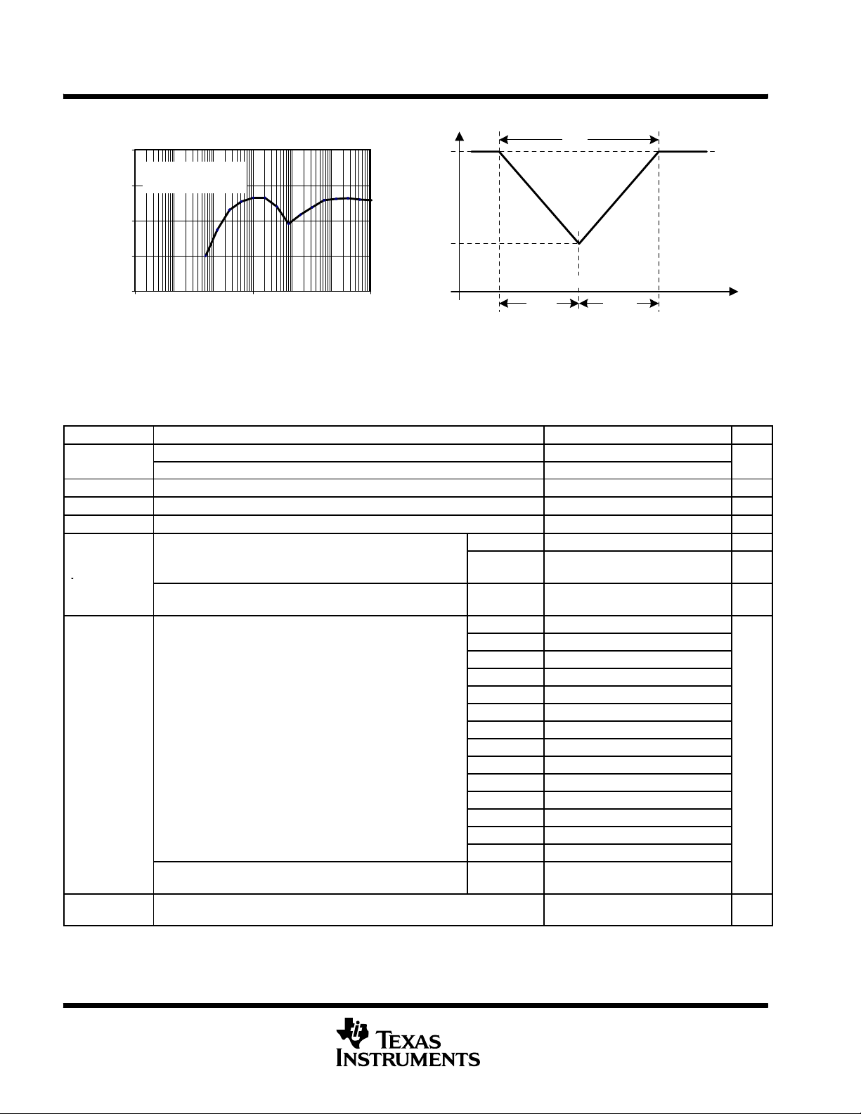
MSP430xG461x
)
V
hys(SVS_I
T--)
/
V
V
MIXED SIGNAL MICROCONTROLLER
SLAS508G -- APRIL 2006 -- REVISED OCTOBER 2007
typical characteristics (continued)
V
CC
2
V
CC
Typical Conditions
1.5
=3V
3V
-- V
1
V
CC(drop)
V
0.5
0
0.001 1 1000
t
-- Pulse Width -- μs
pw
Figure 12. V
CC(drop)
Level With a Triangle Voltage Drop to Generate a POR/Brownout Signal
CC(drop)
electrical characteristics over recommended operating free-air temperature (unless otherwise
noted)
SVS (supply voltage supervisor/monitor) (see Note 1)
PARAMETER TEST CONDITIONS MIN TYP MAX UNIT
t
(SVSR)
t
d(SVSon)
t
settle
V
(SVSstart)
V
hys(SVSIT--
(SVS_IT--)
I
CC(SVS)
(see Note 1)
†
The recommended operating voltage range is limited to 3.6 V.
‡
t
is the settling time that the comparator o/p needs to have a stable level after VLD is switched VLD ≠ 0 to a different VLD value somewhere
settle
between 2 and 15. The overdrive is assumed to be > 50 mV.
NOTE 1: The current consumption of the SVS module is not included in the I
dVCC/dt > 30 V/ms (see Figure 13) 5 150
dVCC/dt ≤ 30 V/ms 2000
SVS on, switch from VLD = 0 to VLD ≠ 0, VCC=3V 20 150 μs
‡
VLD ≠ 0
VLD ≠ 0, VCC/dt ≤ 3 V/s (see Figure 13) 1.55 1.7 V
VLD = 1 70 120 155 mV
VCC/dt ≤ 3 V/s (see Figure 13)
VCC/dt ≤ 3 V/s (see Figure 13), external voltage applied
on A7
VLD = 2 .. 14
VLD = 15 4.4 20 mV
VLD = 1 1.8 1.9 2.05
VLD = 2 1.94 2.1 2.23
VLD = 3 2.05 2.2 2.35
VLD = 4 2.14 2.3 2.46
VLD = 5 2.24 2.4 2.58
VLD = 6 2.33 2.5 2.69
V
dt ≤ 3V/s (see Figure 13)
CC
VLD = 7 2.46 2.65 2.84
VLD = 8 2.58 2.8 2.97
VLD = 9 2.69 2.9 3.10
VLD = 10 2.83 3.05 3.26
VLD = 11 2.94 3.2 3.39
VLD = 12 3.11 3.35 3.58
VLD = 13 3.24 3.5 3.73
VLD = 14 3.43 3.7
VCC/dt ≤ 3 V/s (see Figure 13), external voltage applied
on A7
VLD = 15 1.1 1.2 1.3
VLD ≠ 0, VCC=2.2V/3V 10 15 μA
current consumption data.
CC
t
pw
tf=t
r
t
f
t
r
tpw-- Pulse Width -- μs
V
(SVS_IT--)
x 0.001
†
12 μs
V
(SVS_IT--)
x 0.016
†
†
†
3.96
μs
40
POST OFFICE BOX 655303 • DALLAS, TEXAS 75265
Page 41

typical characteristics
V
V
(SVS_IT--)
V
(SVSstart)
V
(B_IT--)
V
CC(start)
Brownout
SVS
CC
1
0
Out
1
V
hys(SVS_IT--)
V
hys(B_IT--)
Brownout
Region
t
d(BOR)
MIXED SIGNAL MICROCONTROLLER
SLAS508G -- APRIL 2006 -- REVISED OCTOBER 2007
Software Sets VLD>0:
SVS is Active
SVS Circuit is Active From VLD > to VCC<V(
B_IT-- )
MSP430xG461x
Brown-
Out
Region
t
d(BOR)
Set POR
2
1.5
-- V
1
CC(drop)
V
0.5
0
0
1
undefined
0
t
d(SVSon)
Figure 13. SVS Reset (SVSR) vs Supply Voltage
Rectangular Drop
Triangular Drop
1 10 1000
t
-- Pulse Width -- μs
pw
100
V
V
CC(drop)
V
CC
3V
CC
3V
t
d(SVSR)
t
pw
1ns 1ns
t
pw
Figure 14. V
CC(drop)
V
CC(drop)
tf=t
r
t
f
t -- Pulse Width -- μs
t
r
With a Square Voltage Drop and a Triangle Voltage Drop to Generate an SVS Signal
POST OFFICE BOX 655303 • DALLAS, TEXAS 75265
41
Page 42
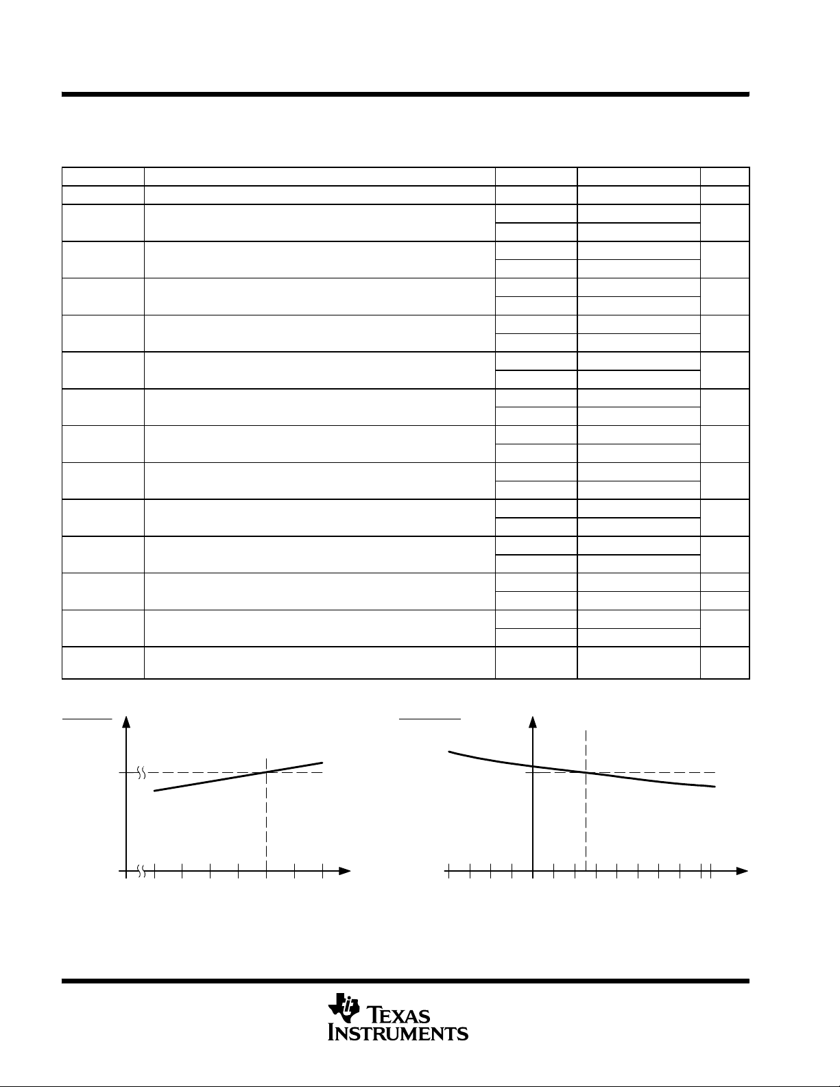
MSP430xG461x
f
f
f
f
f
f
f
f
f
f
StepsizebetweenadjacentDCOtaps:
Temperaturedrif
t,N
(DCO)
=01Eh,FN_8=FN_4=FN_3=FN_2=0
MIXED SIGNAL MICROCONTROLLER
SLAS508G -- APRIL 2006 -- REVISED OCTOBER 2007
electrical characteristics over recommended operating free-air temperature (unless otherwise
noted)
DCO
PARAMETER TEST CONDITIONS V
f
(DCOCLK)
(DCO=2)
(DCO=27)
(DCO=2)
(DCO=27)
(DCO=2)
(DCO=27)
(DCO=2)
(DCO=27)
(DCO=2)
(DCO=27)
S
n
D
t
D
V
N
=01Eh, FN_8=FN_4=FN_3=FN_2=0, D = 2; DCOPLUS= 0 2.2 V/3 V 1 MHz
(DCO)
FN_8=FN_4=FN_3=FN_2=0 ; DCOPLUS = 1
FN_8=FN_4=FN_3=FN_2=0; DCOPLUS = 1
FN_8=FN_4=FN_3=0, FN_2=1; DCOPLUS = 1
FN_8=FN_4=FN_3=0, FN_2=1; DCOPLUS = 1
FN_8=FN_4=0, FN_3= 1, FN_2=x; DCOPLUS = 1
FN_8=FN_4=0, FN_3= 1, FN_2=x; DCOPLUS = 1
FN_8=0, FN_4= 1, FN_3= FN_2=x; DCOPLUS = 1
FN_8=0, FN_4=1, FN_3= FN_2=x; DCOPLUS = 1
FN_8=1, FN_4=FN_3=FN_2=x; DCOPLUS = 1
FN_8=1,FN_4=FN_3=FN_2=x; DCOPLUS = 1
Stepsize between adjacent DCO taps:
Sn=f
DCO(Tap n+1)/fDCO(Tap n)
Temperature drift, N
(see Figure 16 for taps 21 to 27)
= 01Eh, FN_8=FN_4=FN_3=FN_2=0
1<TAP≤ 20 1.06 1.11
D = 2; DCOPLUS = 0
Drift with VCCvariation, N
= 01Eh, FN_8=FN_4=FN_3=FN_2=0
(DCO)
D = 2; DCOPLUS = 0
CC
2.2 V 0.3 0.65 1.25
2.2 V 2.5 5.6 10.5
2.2 V 0.7 1.3 2.3
2.2 V 5.7 10.8 18
2.2 V 1.2 2 3
2.2 V 9 15.5 25
2.2 V 1.8 2.8 4.2
2.2 V 13.5 21.5 33
2.2 V 2.8 4.2 6.2
2.2 V 21 32 46
TAP = 27 1.07 1.17
2.2 V –0.2 –0.3 –0.4
MIN TYP MAX UNIT
3V 0.3 0.7 1.3
3V 2.7 6.1 11.3
3V 0.8 1.5 2.5
3V 6.5 12.1 20
3V 1.3 2.2 3.5
3V 10.3 17.9 28.5
3V 2.1 3.4 5.2
3V 16 26.6 41
3V 4.2 6.3 9.2
3V 30 46 70
3V –0.2 –0.3 –0.4
0 5 15 %/V
MHz
MHz
MHz
MHz
MHz
MHz
MHz
MHz
MHz
MHz
%/_C
f
(DCO)
f
(DCO3V)
1.0
1.8 3.02.4 3.6
f
(DCO)
f
(DCO20°C)
1.0
20 6040 85
0-- 2 0-- 4 00
TA-- °CVCC-- V
Figure 15. DCO Frequency vs Supply Voltage VCCand vs Ambient Temperature
42
POST OFFICE BOX 655303 • DALLAS, TEXAS 75265
Page 43

MSP430xG461x
MIXED SIGNAL MICROCONTROLLER
SLAS508G -- APRIL 2006 -- REVISED OCTOBER 2007
electrical characteristics over recommended operating free-air temperature (unless otherwise
noted) (continued)
1.17
(DCO)
f
- Stepsize Ratio between DCO Taps
S
1.11
1.07
n
1.06
Min
12720
DCO Tap
Max
Figure 16. DCO Tap Step Size
Legend
Tolerance at Tap 27
DCO Frequency
Adjusted by Bits
9
2
to 25in SCFI1 {N
Tol e r a nce at Tap 2
{DCO}
}
FN_2=0
FN_3=0
FN_4=0
FN_8=0
Overlapping DCO Ranges:
Uninterrupted Frequency Range
FN_2=1
FN_3=0
FN_4=0
FN_8=0
FN_2=x
FN_3=1
FN_4=0
FN_8=0
FN_2=x
FN_3=x
FN_4=1
FN_8=0
FN_2=x
FN_3=x
FN_4=x
FN_8=1
Figure 17. Five Overlapping DCO Ranges Controlled by FN_x Bits
POST OFFICE BOX 655303 • DALLAS, TEXAS 75265
43
Page 44

MSP430xG461x
Integratedinputcapacitanc
e
Integratedoutputcapacitance
V
/3V
V
V
/3V
MIXED SIGNAL MICROCONTROLLER
SLAS508G -- APRIL 2006 -- REVISED OCTOBER 2007
electrical characteristics over recommended operating free-air temperature (unless otherwise
noted)
crystal oscillator, LFXT1 oscillator (see Notes 1 and 2)
PARAMETER TEST CONDITIONS MIN TYP MAX UNIT
OSCCAPx = 0h, VCC=2.2V/3V 0
C
XIN
C
XOUT
V
IL
V
IH
NOTES: 1. The parasitic capacitance from the package and board may be estimated to be 2 pF. The effective load capacitor for the crystal is
Integrated input capacitance
(see Note 4)
Integrated output capacitance
(see Note 4)
Input levels at XIN VCC=2.2
(C
XINxCXOUT
2. Toimprove E MI on the l ow-power LFXT1 oscillator,particularly in the LF mode (32 kHz), the following guidelines should be observed.
)/(C
XIN+CXOUT
OSCCAPx = 1h, V
OSCCAPx = 2h, V
OSCCAPx = 3h, VCC=2.2V/3V 18
OSCCAPx = 0h, VCC=2.2V/3V 0
OSCCAPx = 1h, V
OSCCAPx = 2h, V
OSCCAPx = 3h, VCC=2.2V/3V 18
). This is independent of XTS_FLL.
-- Keep as short of a trace as possible between the ’xG461x and the crystal.
-- Design a good ground plane around the oscillator pins.
-- Prevent crosstalk from other clock or data lines into oscillator pins XIN and XOUT.
-- Avoid running PCB traces underneath or adjacent to the XIN and XOUT pins.
-- Use assembly materials and praxis to avoid any parasitic load on the oscillator XIN and XOUT pins.
-- If conformal coating is used, ensure that it does not induce capacitive/resistive leakage between the oscillator pins.
-- Do not route the XOUT line to the JTAG header to support the serial programming adapter as shown in other
documentation. This signal is no longer required for the serial programming adapter.
3. Applies only when using an external logic-level clock source. XTS_FLL must be set. Not applicable when using a crystal or resonator.
4. External capacitance is recommended for precision real-time clock applications; OSCCAPx = 0h.
=2.2V/3V 10
CC
=2.2V/3V 14
CC
=2.2V/3V 10
CC
=2.2V/3V 14
CC
V
(see Note 3)
SS
0.8×V
CC
0.2×V
V
pF
pF
CC
CC
crystal oscillator, XT2 oscillator (see Note 1)
PARAMETER TEST CONDITIONS MIN NOM MAX UNIT
C
XT2IN
C
XT2OUT
V
IL
V
IH
NOTES: 1. The oscillator needs capacitors at both terminals, with values specified by the crystal manufacturer.
Integrated input capacitance VCC=2.2V/3V 2 pF
Integrated output capacitance VCC=2.2V/3V 2 pF
V
Input levels at XT2IN VCC=2.2
2. Applies only when using an external logic-level clock source. Not applicable when using a crystal or resonator.
(see Note 2)
SS
0.8 × V
CC
0.2 × V
V
CC
CC
V
V
44
POST OFFICE BOX 655303 • DALLAS, TEXAS 75265
Page 45
MSP430xG461x
UARTreceivedeglitchtime
UCLKedgetoSIMOvalid
;
UCLKedgetoSOMIvalid
;
MIXED SIGNAL MICROCONTROLLER
SLAS508G -- APRIL 2006 -- REVISED OCTOBER 2007
electrical characteristics over recommended ranges of supply voltage and operating free-air
temperature (unless otherwise noted) (continued)
USCI (UART Mode)
PARAMETER TEST CONDITIONS VCC MIN TYP MAX UNIT
Internal: SMCLK, ACLK
f
USCI
f
BITCLK
t
τ
USCI input clock frequency
BITCLK clock frequency
(equals Baudrate in MBaud)
UART receive deglitch time
(see Note 1)
NOTE 1: Pulses on the UART receive input (UCxRX) shorter than the UART receive deglitch time are suppressed. To ensure that pulses are
correctly recognized their width should exceed the maximum specification of the deglitch time.
USCI (SPI Master Mode, see Figure 18 and Figure 19)
PARAMETER TEST CONDITIONS VCC MIN TYP MAX UNIT
f
USCI
t
SU,MI
t
HD,MI
t
VAL ID, M O
USCI input clock frequency
SOMI input data setup time
SOMI input data hold time
SIMO output data valid time
External: UCLK
Duty Cycle = 50% ± 10%
SMCLK, ACLK
Duty Cycle = 50% ± 10%
UCLK edgetoSIMOvalid;
CL=20pF
f
SYSTEM
MHz
2.2V /3 V 1 MHz
2.2 V 50 150 600
3V 50 100 600
f
SYSTEM
2.2 V 11 0
3V 75
2.2 V 0
3V 0
2.2 V 30
3V 20
ns
MHz
ns
ns
ns
USCI (SPI Slave Mode, see Figure 20 and Figure 21)
PARAMETER TEST CONDITIONS VCC MIN TYP MAX UNIT
t
STE,LEAD
t
STE,LAG
t
STE,ACC
t
STE,DIS
t
SU,SI
t
HD,SI
t
VAL ID, S O
STE lead time
STE low to clock
STE lag time
Last clock to STE high
STE access time
STE low to SOMI data out
STE disable time
STE high to SOMI high impedance
SIMO input data setup time
SIMO input data hold time
SOMI output data valid time
UCLK edgetoSOMIvalid;
CL=20pF
2.2 V/3 V 50 ns
2.2 V/3 V 10 ns
2.2 V/3 V 50 ns
2.2 V/3 V 50 ns
2.2 V 20
3V 15
2.2 V 10
3V 10
2.2 V 75 110
3V 50 75
ns
ns
ns
POST OFFICE BOX 655303 • DALLAS, TEXAS 75265
45
Page 46

MSP430xG461x
MIXED SIGNAL MICROCONTROLLER
SLAS508G -- APRIL 2006 -- REVISED OCTOBER 2007
electrical characteristics over recommended ranges of supply voltage and operating free-air
temperature (unless otherwise noted) (continued)
1/f
UCxCLK
CKPL = 0
UCLK
CKPL = 1
SOMI
SIMO
t
LOW/HIGHtLOW/HIGH
Figure 18. SPI Master Mode, CKPH = 0
t
VAL ID ,M O
t
SU,MI
t
HD,MI
UCLK
SOMI
SIMO
CKPL = 0
CKPL = 1
1/f
UCxCLK
t
LOW/HIGHtLOW/HIGH
t
SU,MI
t
VAL ID ,M O
Figure 19. SPI Master Mode, CKPH = 1
t
HD,MI
46
POST OFFICE BOX 655303 • DALLAS, TEXAS 75265
Page 47

MSP430xG461x
MIXED SIGNAL MICROCONTROLLER
SLAS508G -- APRIL 2006 -- REVISED OCTOBER 2007
electrical characteristics over recommended ranges of supply voltage and operating free-air
temperature (unless otherwise noted) (continued)
STE
UCLK
SIMO
SOMI
STE
CKPL = 0
CKPL = 1
t
STE,LEAD
1/f
UCxCLK
t
LOW/HIGHtLOW/HIGH
t
ACC
t
VAL ID ,S OM I
Figure 20. SPI Slave Mode, CKPH = 0
t
STE, LEAD
t
SU,SIMO
t
HD,SIMO
t
STE,LAG
t
STE,LAG
t
DIS
UCLK
SIMO
SOMI
CKPL=0
CKPL=1
1/f
UCxCLK
t
LOW/HIGHtLOW/HIGH
t
ACC
t
VAL ID ,S O
Figure 21. SPI Slave Mode, CKPH = 1
t
SU,SI
t
HD,SI
t
DIS
POST OFFICE BOX 655303 • DALLAS, TEXAS 75265
47
Page 48

MSP430xG461x
p
p
y
Pulsewidthofspikessuppressedb
y
MIXED SIGNAL MICROCONTROLLER
SLAS508G -- APRIL 2006 -- REVISED OCTOBER 2007
electrical characteristics over recommended ranges of supply voltage and operating free-air
temperature (unless otherwise noted) (continued)
USCI (I2C Mode, see Figure 22)
PARAMETER TEST CONDITIONS VCC MIN TYP MAX UNIT
Internal: SMCLK, ACLK
f
USCI
f
SCL
t
HD,STA
t
SU,STA
t
HD,DAT
t
SU,DAT
t
SU,STO
t
SP
USCI input clock frequency
SCL clock frequency 2.2 V/3 V 0 400 kHz
Hold time (repeated) START
Set--up timefor a repeated START
Data hold time 2.2 V/3 V 0 ns
Data set--up time 2.2 V/3 V 250 ns
Set--uptimeforSTOP 2.2 V/3 V 4.0 μs
Pulse width ofspikes su
ressed b
input filter
External: UCLK
Duty Cycle = 50% ± 10%
f
≤ 100kHz 2.2 V/3 V 4.0
SCL
f
> 100kHz 2.2 V/3 V 0.6
SCL
f
≤ 100kHz 2.2 V/3 V 4.7
SCL
f
> 100kHz 2.2 V/3 V 0.6
SCL
2.2 V 50 150 600
3V 50 100 600
f
SYSTEM
MHz
μs
μs
ns
SDA
SCL
t
HD ,STA
t
t
LOW
HIGH
t
HD ,DAT
t
SU , DAT
t
SU , STAtHD ,STA
t
SP
t
SU , STO
Figure 22. I2C Mode Timing
USART1 (see Note 1)
PARAMETER TEST CONDITIONS MIN TYP MAX UNIT
t
(τ)
USART1 deglitch time
NOTE 1: The signal applied to the USART1 receive signal/terminal (URXD1) should meet the timing requirements of t
flip-flop is set. The URXS flip-flop is set with negative pulses meeting the minimum-timing condition of t
set the flag must be met independently from this timing constraint. The deglitch circuitry is active only on negative transitions on the
URXD1 line.
VCC= 2.2 V, SYNC = 0, UART mode 200 430 800
VCC= 3 V, SYNC = 0, UART mode 150 280 500
(τ
)
t
BUF
ns
to ensure that the URXS
(τ
)
. The operating conditions to
48
POST OFFICE BOX 655303 • DALLAS, TEXAS 75265
Page 49

MSP430xG461x
A
A
(seeNote4)A
A
MIXED SIGNAL MICROCONTROLLER
SLAS508G -- APRIL 2006 -- REVISED OCTOBER 2007
electrical characteristics over recommended operating free-air temperature (unless otherwise
noted) (continued)
12-bit ADC, power supply and input range conditions (see Note 1)
PARAMETER TEST CONDITIONS MIN TYP MAX UNIT
AVCCand DVCCare connected together,
AV
AV
CC
V
(P6.x/Ax)
Analog supply voltage
Analog input voltage
range (see Note 2)
Operating supply current
I
ADC12
intoAVCCterminal
(see Note 3)
Operating supply current
I
REF+
into AVCCterminal
(see Note 4)
C
I
R
I
Input capacitance
Input MUX ON resistance 0V ≤ VAx≤ V
NOTES: 1. The leakage current is defined in the leakage current table with A x parameter.
2. The analog input voltage range must be within the selected reference voltage range V
3. The internal reference supply current is not included in current consumption parameter I
4. The internal reference current is supplied via terminal AV
conversion is active. The REFON bit enables to settle the built-in reference before starting an A/D conversion.
and DVSSare connected together,
SS
V
(AVSS)=V(DVSS)
=0V
All external Ax terminals. Analog inputs
selected in ADC12MCTLx register and P6Sel.x=1,
V
≤ VAx≤ V
(AVSS)
f
ADC12CLK
(AVCC)
=5.0MHz,
VCC=2.2V 0.65 1.3
DC12ON = 1, REFON = 0,
SHT0=0, SHT1=0, ADC12DIV=0
f
ADC12CLK
=5.0MHz,
ADC12ON = 0,
VCC=3V 0.8 1.6
VCC=3V 0.5 0.8 mA
REFON = 1, REF2_5V = 1
f
ADC12CLK
=5.0MHz,
VCC=2.2V 0.5 0.8
DC12ON = 0,
REFON = 1, REF2_5V = 0
Only one terminal can be selected
at one time, Ax
AVC C
. Consumption is independent of the ADC12ON control bit, unless a
CC
VCC=3V 0.5 0.8
VCC=2.2V 40 pF
VCC=3V 2000 Ω
R+
2.2 3.6 V
0 V
to V
for valid conversion results.
R--
.
ADC12
AVC C
V
m
m
12-bit ADC, external reference (see Note 1)
PARAMETER TEST CONDITIONS MIN TYP MAX UNIT
V
eREF+
V
REF-- /VeREF--
(V
--
eREF+
V
REF--/VeREF--
I
VeREF+
I
VREF--/VeREF--
NOTES: 1. The external reference is used during conversion to charge and discharge the capacitance array. The input capacitance, CI,isalso
2. The accuracy limits the minimum positive external reference voltage. Lower reference voltage levels may be applied with reduced
3. The accuracy limits the maximum negative external reference voltage. Higher reference voltage levels may be applied with reduced
4. The accuracy limits minimum external differential reference voltage. Lower differential reference voltage levels may be applied with
Positive external
reference voltage input
Negative external
reference voltage input
Differential external
reference voltage input
)
Input leakage current 0V ≤V
Input leakage current 0V ≤ V
V
eREF+>VREF--/VeREF--
V
eREF+>VREF--/VeREF--
V
eREF+>VREF--/VeREF--
≤ V
eREF+
eREF--
≤ V
AVC C
AVC C
,(seeNote2) 1.4 V
AVC C
,(seeNote3) 0 1.2 V
,(seeNote4) 1.4 V
AVC C
VCC=2.2V/3V ±1 μA
VCC=2.2V/3V ±1 μA
V
V
the dynamic load for an external reference during conversion. The dynamic impedance of the reference supply should follow the
recommendations on analog-source impedance to allow the charge to settle for 12-bit accuracy.
accuracy requirements.
accuracy requirements.
reduced accuracy requirements.
POST OFFICE BOX 655303 • DALLAS, TEXAS 75265
49
Page 50

MSP430xG461x
Positivebuiltinreferenc
e
V
)
A
VCCminimumvoltag
e
A
V
CC(min)
Positivebuiltinreferenc
e
V
LoadcurrentoutofV
REF
A
A
Loadcurrentregulation
Loadcurrentregulation
x
V
V
V
MIXED SIGNAL MICROCONTROLLER
SLAS508G -- APRIL 2006 -- REVISED OCTOBER 2007
electrical characteristics over recommended operating free-air temperature (unless otherwise
noted) (continued)
12-bit ADC, built-in reference
PARAMETER TEST CONDITIONS MIN NOM MAX UNIT
REF2_5V = 1 for 2.5 V,
V
REF+
AV
I
VREF+
CC(min
Positive built-in reference
voltage output
Positive built-in reference
active
Load current out ofV
terminal
max ≤ I
VREF+
REF2_5V = 0 for 1.5 V,
I
max ≤ I
VREF+
REF2_5V = 0, I
,
REF2_5V = 1, I
REF2_5V = 1, I
+
I
= 500 μA +/-- 100 μA,
VREF+
VREF+
VREF+
VREF+
VREF+
VREF+
≤ I
VREF+
≤ I
VREF+
max ≤ I
min ≥ I
min ≥ I
min
min
VREF+
VREF+
VREF+
I
nalog input voltage ~0.75V;
I
L(VREF)+
Load-current regulation
V
terminal
REF+
REF2_5V = 0
I
= 500 μA ± 100 μA,
VREF+
Analog input voltage ~1.25 V,
REF2_5V = 1
I
=100 μA → 900 μA,
I
DL(VREF) +
C
VREF+
T
REF+
t
REFON
Load current regulation
V
terminal
REF+
Capacitance at pin V
(see Note 1)
Temperature coefficient of
built-in reference
Settle time of internal
reference voltage (see
Figure 23 and Note 2)
VREF+
=5 μF, ax~0.5
C
VREF+
Error of conversion result ≤ 1LSB
REFON =1,
REF+
0mA≤ I
I
VREF+
0mA≤ I
I
VREF+
V
REF+
≤ I
VREF+
is a constant in the range of
≤ 1mA
VREF+
=0.5mA,C
=1.5V,V
AVC C
VREF+
VREF+
REF+
max
=10μF,
=2.2V
NOTES: 1. The internal buffer operational amplifier and the accuracy specifications require an external capacitor. All INL and DNL tests uses
two capacitors between pins V
2. The condition is that the error in a conversion started after t
and AVSSand V
REF+
REF--/VeREF--
REFON
and AVSS:10μF tantalum and 100 nF ceramic.
is less than ±0.5 LSB. The settling time depends on the external
capacitive load.
C
VREF+
100 μF
VCC=3V 2.4 2.5 2.6
VCC=
2.2 V/3 V
≤ I
min 2.2
VREF+
1.44 1.5 1.56
≥ --0.5mA 2.8
≥ -- 1 m A 2.9
VCC=2.2V 0.01 -- 0 . 5
VCC=3V 0.01 -- 1
VCC=2.2V ±2
VCC=3V ±2
VCC=3V ±2 LSB
,
=3
CC
VCC=
2.2 V/3 V
5 10 μF
VCC=
2.2 V/3 V
V
m
LSB
20 ns
±100 ppm/°C
17 ms
10 μF
REFON
≈ .66xC
VREF+
[ms] with C
VREF+
in μF
t
1 μF
0
1ms
Figure 23. Typical Settling Time of Internal Reference t
50
POST OFFICE BOX 655303 • DALLAS, TEXAS 75265
10 ms
100 ms t
REFON
REFON
vs External Capacitor on V
REF
+
Page 51

MSP430xG461x
MIXED SIGNAL MICROCONTROLLER
SLAS508G -- APRIL 2006 -- REVISED OCTOBER 2007
From
Power
Supply
+
--
10 μ F 100 nF
+
--
10 μ F 100 nF
Apply External Reference [V
or Use Internal Reference [V
eREF+
REF+
]
]
+
--
Apply
External
Reference
10 μ F 100 nF
+
--
10 μ F 100 nF
Figure 24. Supply Voltage and Reference Voltage Design V
From
Power
Supply
+
--
10 μ F 100 nF
DV
DV
AV
AV
V
V
DV
DV
CC1/2
SS1/2
CC
MSP430FG461x
SS
or V
REF+
-- / V
REF
eREF--
CC1/2
SS1/2
eREF+
REF--/VeREF--
External Supply
+
--
10 μ F 100 nF
Apply External Reference [V
or Use Internal Reference [V
eREF+
REF+
]
]
+
--
10 μ F 100 nF
Reference Is Internally
Switched to AV
SS
Figure 25. Supply Voltage and Reference Voltage Design V
AV
CC
MSP430FG461x
AV
SS
or V
V
REF+
V
REF--/VeREF--
REF--/VeREF--
eREF+
=AVSS, Internally Connected
POST OFFICE BOX 655303 • DALLAS, TEXAS 75265
51
Page 52
MSP430xG461x
]
x
V
V
C
C
=
MIXED SIGNAL MICROCONTROLLER
SLAS508G -- APRIL 2006 -- REVISED OCTOBER 2007
electrical characteristics over recommended operating free-air temperature (unless otherwise
noted) (continued)
12-bit ADC, timing parameters
PARAMETER TEST CONDITIONS MIN NOM MAX UNIT
f
ADC12CLK
f
ADC12OSC
t
CONVERT
t
ADC12ON
t
Sample
Internal ADC12
oscillator
Conversion time
Turn on settling time
of the ADC
Sampling time
NOTES: 1. The condition is that the error in a conversion started after t
settled.
2. Approximately ten Tau (τ) are needed to get an error of less than ±0.5 LSB:
t
Sample
=ln(2
n+1
)x(RS+RI)xCI+ 800 ns where n = ADC resolution = 12, RS= external source resistance.
12-bit ADC, linearity parameters
PARAMETER TEST CONDITIONS MIN NOM MAX UNIT
EIIntegral linearity error
Differential linearity
E
D
error
E
Offset error
O
E
Gain error
G
Total unadjusted
E
T
error
1.4 V ≤ (V
1.6 V < (V
(V
C
(V
Internal impedance of source R
C
(V
C
(V
C
For specified performance of
ADC12 linearity parameters
ADC12DIV=0,
f
ADC12CLK=fADC12OSC
C
≥ 5 μF, Internal oscillator,
VREF+
f
ADC12OSC
External f
= 3.7 MHz to 6.3 MHz
ADC12CLK
from ACLK, MCLK, or SMCLK,
ADC12SSEL ≠ 0
VCC=2.2V/3V 0.45 5 6.3 MHz
VCC=2.2V/3V 3.7 5 6.3 MHz
VCC=2.2V/3V 2.06 3.51 μs
13×ADC12DIV×
1/f
ADC12CLK
(see Note 1) 100 ns
RS= 400 Ω,RI= 1000 Ω,
CI=30pF,τ =[RS+R
I
(see Note 2)
-- V
eREF+
eREF+
-- V
eREF+
=10μF (tantalum) and 100 nF (ceramic)
VREF+
-- V
eREF+
=10μF (tantalum) and 100 nF (ceramic)
VREF+
-- V
eREF+
=10μF (tantalum) and 100 nF (ceramic)
VREF+
-- V
eREF+
=10μF (tantalum) and 100 nF (ceramic)
VREF+
REF--/VeREF--
-- V
REF--/VeREF--
REF--/VeREF--)min
REF--/VeREF--)min
REF--/VeREF--)min
REF--/VeREF--)min
)min≤ 1.6 V
)min≤ [V
≤ (V
eREF+
≤ (V
eREF+
< 100 Ω,
S
≤ (V
eREF+
≤ (V
eREF+
CI,
VCC=3V 1220
VCC=2.2V 1400
ADC12ON
-- V
-- V
-- V
-- V
is less than ±0.5 LSB. The reference and input signal are already
]
AVC C
REF--/VeREF--
REF--/VeREF--
REF--/VeREF--
REF--/VeREF--
),
),
),
),
=
2.2 V/3 V
VCC=
2.2 V/3 V
VCC=
2.2 V/3 V
VCC=
2.2 V/3 V
VCC=
2.2 V/3 V
±2 ±4 LSB
±1.1 ±2 LSB
±2 ±5 LSB
±2
±1.7
±1 LSB
μs
ns
LSB
52
POST OFFICE BOX 655303 • DALLAS, TEXAS 75265
Page 53

MSP430xG461x
p
ply
Operatingsupplycurrentint
o
REFON=0,INCH=0A
h
A
A
V
/
ADC12ON=1,INCH=0A
h
2.2V/
V
V
/
A
2.2V/
V
/
A
ADC12ON=1,INCH=0A
h
Currentintodividera
t
A
A
A
A
ADC12ON=1,INCH=0B
h
V
A
ADC12ON=1,INCH=0B
h
V
/3V
A
MIXED SIGNAL MICROCONTROLLER
SLAS508G -- APRIL 2006 -- REVISED OCTOBER 2007
electrical characteristics over recommended operating free-air temperature (unless otherwise
noted) (continued)
12-bit ADC, temperature sensor and built-in V
PARAMETER
I
SENSOR
V
SENSOR
TC
SENSOR
Operatingsu
AVCCterminal (see Note 1)
(see Note 2)
Sample time required if
t
SENSOR(sample)
I
VMID
V
MID
channel 10 is selected
(see Note 3)
Current into divider at
channel 11 (see Note 4)
VCCdivider at channel 11
Sample time required if
t
VMID(sample)
channel 11 is selected
(see Note 5)
NOTES: 1. The sensor current I
is high). W hen REFON = 1, I
2. The temperature sensor offset can be as much as ±20_C. A single-point calibration is recommended in order to minimize the offset
error of the built-in temperature sensor.
3. The typical equivalent impedance of the sensor is 51 k Ω. The sample time required includes the sensor-on time t
4. No additional current is needed. The V
5. The on-time t
VMID(on)
current into REFON = 0, INCH = 0Ah,
ADC12ON=NA, T
DC12ON = 1, INCH = 0Ah, 2.2
T
=0°C
A
DC12ON = 1, INCH = 0Ah
DC12ON = 1, INCH = 0Ah,
Error of conversion result ≤ 1LSB
DC12ON = 1, INCH = 0Bh
DC12ON = 1, INCH = 0Bh,
V
MID
DC12ON = 1, INCH = 0Bh,
Error of conversion result ≤ 1LSB
is consumed if (ADC12ON = 1 and REFON=1), or (ADC12ON=1 AND INCH=0Ah and sample signal
SENSOR
is already included in I
SENSOR
MID
is used during sampling.
is included in the sampling time t
MID
TEST CONDITIONS V
,
=25_C
A
,
,
,
is ~0.5 x V
AVC C
,
.
REF+
VMID(sample)
; no additional on time is needed.
MIN NOM MAX UNIT
CC
2.2 V 40 120
3V 60 160
3V
2.2
3V
986 m
3.55±3% m
2.2 V 30
3V 30
2.2 V NA
3V NA
2.2 V 1.1 1.1±0.04
3V 1.5 1.50±0.04
2.2 V 1400
3V 1220
SENSOR(on)
μ
°C
μs
μ
ns
12-bit DAC, supply specifications
AV
PARAMETER TEST CONDITIONS V
Analog supply voltage
CC
AV
CC =DVCC
AV
SS
,
=DVSS=0 V
CC
DAC12AMPx=2, DAC12IR=0,
DAC12_xDAT=0800h
DAC12AMPx=2, DAC12IR=1,
DAC12_xDAT=0800h
,VeREF+=VREF+
DAC12AMPx=5, DAC12IR=1,
DAC12_xDAT=0800h, V
eREF+=VREF+
=AV
=AV
CC
CC
2.2
I
DD
Supply current:
Single DAC Channel
(see Notes 1 and 2)
DAC12AMPx=7, DAC12IR=1,
PSRR
Power-supply
rejection ratio
(see Notes 3 and 4)
DAC12_xDAT=0800h, V
DAC12_xDAT = 800h, V
∆AV
= 100mV
CC
DAC12_xDAT = 800h, V
∆AV
= 100mV
CC
eREF+=VREF+
=1.5V,
REF
= 1.5 V or 2.5 V,
REF
=AV
CC
2.2 V
3V
NOTES: 1. No load at the output pin, DAC12_0 or DAC12_1, assuming that the control bits for the shared pins are set properly.
2. Current into reference terminals not included. If DAC12IR = 1 current flows through the input divider; see Reference Input
specifications.
3. PSRR = 20*log{∆AV
4. V
is applied externally. The internal reference is not used.
REF
CC
/∆V
DAC12_xOUT
}.
MIN TYP MAX UNIT
2.20 3.60 V
50 110
50 110
200 440
700 1500
70 dB
μ
POST OFFICE BOX 655303 • DALLAS, TEXAS 75265
53
Page 54

MSP430xG461x
Integralnonlinearit
y
Differentialnonlinearit
y
V
f
f
t
Offset_Ca
l
2.2V/3V6m
s
MIXED SIGNAL MICROCONTROLLER
SLAS508G -- APRIL 2006 -- REVISED OCTOBER 2007
electrical characteristics over recommended operating free-air temperature (unless otherwise
noted) (continued)
12-bit DAC, linearity specifications (see Figure 26)
PARAMETER TEST CONDITIONS V
CC
Resolution (12-bit Monotonic) 12 bits
V
=1.5V,
INL
DNL
E
O
d
E(O)/dT
Integral nonlinearity
(see Note 1)
Differential nonlinearity
(see Note 1)
Offset voltage without
calibration
(see Notes 1, 2)
Offset voltage with
calibration
(see Notes 1, 2)
Offset error
temperature coefficient
ref
DAC12AMPx = 7, DAC12IR = 1
V
=2.5V,
ref
DAC12AMPx = 7, DAC12IR = 1
V
=1.5V,
ref
DAC12AMPx = 7, DAC12IR = 1
V
=2.5V,
ref
DAC12AMPx = 7, DAC12IR = 1
V
=1.5V,
ref
DAC12AMPx = 7, DAC12IR = 1
V
=2.5V,
ref
DAC12AMPx = 7, DAC12IR = 1
V
=1.5V,
ref
DAC12AMPx = 7, DAC12IR = 1
V
=2.5V,
ref
DAC12AMPx = 7, DAC12IR = 1
2.2 V
3V
2.2 V
3V
2.2 V
3V
2.2 V
3V
2.2 V/3 V ±30 μV/°C
(see Note 1)
V
=1.5V 2.2 V
E
G
d
E(G)/dT
t
Offset Cal
Gainerror(seeNote1)
Gain temperature
coefficient (see Note 1)
Timefor o
set calibration
(see Note 3)
REF
V
=2.5V 3V
REF
2.2 V/3 V 10
DAC12AMPx = 2 100
DAC12AMPx = 3,5
2.2 V/3 V
DAC12AMPx = 4,6,7
NOTES: 1. Parameters calculated from the best -fit curve from 0x0A to 0xFFF. The best-fit curve method is used to deliver coefficients “a” and
“b” of the first order equation: y = a + b*x. V
DAC12_xOUT=EO
+(1+EG)*(V
/4095) * DAC12_xDAT, DAC12IR = 1.
eREF+
2. The offset calibration works on the output operational amplifier. Offset Calibration is triggered setting bit DAC12CALON
3. The offset calibration can be done if DAC12AMPx = {2, 3, 4, 5, 6, 7}. The output operational amplifier is switched off with
DAC12AMPx = {0, 1}. It is recommended that the DAC12 module be configured prior to initiating calibration. Port activity during
calibration may effect accuracy and is not recommended.
MIN TYP MAX UNIT
±2.0 ±8.0 LSB
±0.4 ±1.0 LSB
±21
m
±2.5
±3.50 % FSR
ppm of
FSR/°C
32
ms
DAC V
OUT
DAC Output
R
Load
=
AV
CC
V
R+
Ideal transfer
function
2
C
Load
= 100pF
Offset Error
Positive
Negative
Gain Error
DAC Code
Figure 26. Linearity Test Load Conditions and Gain/Offset Definition
54
POST OFFICE BOX 655303 • DALLAS, TEXAS 75265
Page 55

MSP430xG461x
MIXED SIGNAL MICROCONTROLLER
SLAS508G -- APRIL 2006 -- REVISED OCTOBER 2007
electrical characteristics over recommended operating free-air temperature (unless otherwise
noted) (continued)
12-bit DAC, linearity specifications (continued)
TYPICAL INL ERROR
vs
DIGITAL INPUT DATA
4
VCC=2.2V,V
DAC12AMPx = 7
3
DAC12IR = 1
2
1
0
-- 1
REF
=1.5V
-- 2
INL -- Integral Nonlinearity Error -- LSB
-- 3
-- 4
0 512 1024 1536 2048 2560 3072 3584
DAC12_xDAT -- Digital Code
TYPICAL DNL ERROR
vs
DIGITAL INPUT DATA
2.0
1.5
1.0
0.5
0.0
-- 0 . 5
-- 1 . 0
VCC=2.2V,V
DAC12AMPx = 7
DAC12IR = 1
REF
=1.5V
4095
-- 1 . 5
DNL -- Differential Nonlinearity Error -- LSB
-- 2 . 0
0 512 1024 1536 2048 2560 3072 3584
DAC12_xDAT -- Digital Code
POST OFFICE BOX 655303 • DALLAS, TEXAS 75265
4095
55
Page 56
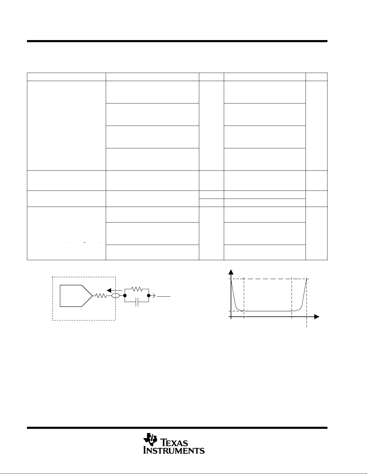
MSP430xG461x
g
range
V
/3V
V
MaxDAC1
2
A
(g)
MIXED SIGNAL MICROCONTROLLER
SLAS508G -- APRIL 2006 -- REVISED OCTOBER 2007
electrical characteristics over recommended operating free-air temperature (unless otherwise
noted) (continued)
12-bit DAC, output specifications
PARAMETER TEST CONDITIONS V
No Load, Ve
REF+
=AVCC,
DAC12_xDAT = 0h, DAC12IR = 1,
DAC12AMPx = 7
No Load, Ve
Output voltage
ran
V
O
e
(see Note 1,
Figure 29)
DAC12_xDAT = 0FFFh, DAC12IR = 1,
DAC12AMPx = 7
=3kΩ,Ve
R
Load
DAC12_xDAT = 0h, DAC12IR = 1,
REF+
=AVCC,
REF+
=AVCC,
DAC12AMPx = 7
R
=3kΩ,Ve
Load
REF+
=AVCC,
DAC12_xDAT = 0FFFh, DAC12IR = 1,
DAC12AMPx = 7
Max DAC12
C
L(DAC12)
load
capacitance
I
L(DAC12)
Max DAC12
load current
R
Load
=3kΩ,V
O/P(DAC12)
< 0.3 V,
DAC12AMPx = 2, DAC12_xDAT = 0h
R
=3kΩ,
Load
V
O/P(DAC12)
> AVCC-- 0 . 3 V
DAC12_xDAT = 0FFFh
R
=3kΩ,
Load
0.3V ≤ V
O/P(DAC12)
≤ AVCC-- 0.3V
R
O/P(DAC12)
Output
resistance
(see Figure 29)
NOTE 1: Data is valid after the offset calibration of the output amplifier.
R
C
Load
Load
= 100pF
AV
CC
2
DAC12
I
Load
O/P(DAC12_x)
Figure 29. DAC12_x Output Resistance Tests
CC
2.2
2.2V/3V 100 pF
2.2V -- 0 . 5 +0.5
3V -- 1 . 0 +1.0
2.2 V/3 V
R
O/P(DAC12_x)
Max
Min
MIN TYP MAX UNIT
0 0.005
AVCC--0.05 AV
0 0.1
AVCC--0.13 AV
150 250
150 250
1 4
0.3
AVCC--0.3V
CC
CC
AV
CC
m
V
Ω
OUT
56
POST OFFICE BOX 655303 • DALLAS, TEXAS 75265
Page 57

MSP430xG461x
Referenceinpu
t
V
/3V
V
(VREF+)
,
p
2.2V/3V
DAC12_xDAT=800h
V
t
O
N
Error
V(O
)
<±0.5LS
B
2.2V/3V
μ
s
)
t
S(FS)
f
2.2V/3V
μ
s
)
DAC12_xDAT=
t
S(C-C
)
3F8h408h3F8
h
2.2V/3V
μ
s
DAC12_xDAT=
SRSlewrate80hF7Fh80
h
2.2V/3V
V
/μs
Glitchenergy,fullscal
e
2.2V/3V30nVs
MIXED SIGNAL MICROCONTROLLER
SLAS508G -- APRIL 2006 -- REVISED OCTOBER 2007
electrical characteristics over recommended operating free-air temperature (unless otherwise
noted)
12-bit DAC, reference input specifications
Ve
PARAMETER TEST CONDITIONS V
REF+
Reference input
voltage range
DAC12IR=0 (see Notes 1 and 2)
DAC12IR=1 (see Notes 3 and 4)
CC
2.2
DAC12_0 IR=DAC12_1 IR =0 20 MΩ
DAC12_0 IR=1, DAC12_1 IR = 0
Ri
Ri
, Reference input
(VREF+)
(VeREF+)
resistance
DAC12_0 IR=0, DAC12_1 IR = 1
DAC12_0 IR=DAC12_1 IR =1,
DAC12_0 SREFx = DAC12_1 SREFx
(see Note 5)
NOTES: 1. For a full-scale output, the reference input voltage can be as high as 1/3 of the maximum output voltage swing (AVCC).
2. The maximum voltage applied at reference input voltage terminal Ve
REF+
=[AVCC-- V
3. For a full-scale output, the reference input voltage can be as high as the maximum output voltage swing (AV
4. The maximum voltage applied at reference input voltage terminal Ve
REF+
=[AVCC-- V
5. When DAC12IR = 1 and DAC12SREFx = 0 or 1 for both channels, the reference input resistive dividers for each DAC are in parallel
reducing the reference input resistance.
MIN TYP MAX UNIT
AVCC/3 AVCC+0.2
AVc c AVcc+0.2
40 48 56
20 24 28
]/[3*(1+EG)].
E(O)
]/(1+EG).
E(O)
CC
).
kΩ
12-bit DAC, dynamic specifications; V
ref=VCC
, DAC12IR = 1 (see Figure 30 and Figure 31)
PARAMETER TEST CONDITIONS V
t
ON
t
S(FS
t
S(C-C
DAC12
on-time
Settling time,
ull-scale 80h→ F7Fh→ 80h
Settling time,
code to code
SR Slew rate
Glitch energy, full-scale
NOTES: 1. R
Load
DAC12_xDAT = 800h,
Error
(see Note 1,Figure 30)
DAC12_xDAT=
DAC12_xDAT=
3F8h→ 408h→ 3F8h
BF8h→ C08h→ BF8h
DAC12_xDAT=
80h→ F7Fh→ 80h
(see Note 2)
DAC12_xDAT=
80h→ F7Fh→ 80h
and C
connected to AVSS(not AVCC/2) in Figure 30.
Load
< ±0.5 LSB
(O)
DAC12AMPx = 0 → {2,3,4} 60 120
,
DAC12AMPx = 0 → {5, 6}
DAC12AMPx = 0 → 7
DAC12AMPx = 2 100 200
DAC12AMPx = 3,5
DAC12AMPx = 4,6,7
DAC12AMPx = 2 5
DAC12AMPx = 3,5
DAC12AMPx = 4,6,7
DAC12AMPx = 2 0.05 0.12
DAC12AMPx = 3,5
DAC12AMPx = 4,6,7
DAC12AMPx = 2 600
DAC12AMPx = 3,5
DAC12AMPx = 4,6,7
2. Slew rate applies to output voltage steps >= 200mV.
Conversion 1 Conversion 2
CC
V
OUT
Glitch
Energy
DAC Output
I
Load
R
Load
=3kΩ
AV
2
C
= 100pF
R
O/P(DAC12.x)
Load
CC
2.2 V/3 V
2.2 V/3 V
2.2 V/3 V
2.2 V/3 V
2.2 V/3 V
+/-- 1/2 LSB
MIN TYP MAX UNIT
15 30
μs
6 12
40 80
μs
15 30
2
μs
1
0.35 0.7
V/μs
1.5 2.7
150
nV-s
Conversion 3
+/-- 1/2 LSB
t
settleLH
t
settleHL
Figure 30. Settling Time and Glitch Energy Testing
POST OFFICE BOX 655303 • DALLAS, TEXAS 75265
57
Page 58

MSP430xG461x
V
/3V
MIXED SIGNAL MICROCONTROLLER
SLAS508G -- APRIL 2006 -- REVISED OCTOBER 2007
electrical characteristics over recommended operating free-air temperature (unless otherwise
noted)
V
Conversion 1 Conversion 2
OUT
Conversion 3
90%
10%
t
Figure 31. Slew Rate Testing
12-bit DAC, dynamic specifications continued (T
PARAMETER TEST CONDITIONS V
DAC12AMPx = {2, 3, 4}, DAC12SREFx = 2,
3-dB bandwidth,
BW
--3dB
Channel-to-channel crosstalk
(see Note 1 and Figure 33)
NOTE 1: R
V
=1.5V, VAC=0.1V
DC
(see Figure 32)
=3kΩ,C
LOAD
LOAD
= 100 pF
DAC12IR = 1, DAC12_xDAT = 800h
DAC12AMPx = {5, 6}, DAC12SREFx = 2,
PP
DAC12IR = 1, DAC12_xDAT = 800h
DAC12AMPx = 7, DAC12SREFx = 2,
DAC12IR = 1, DAC12_xDAT = 800h
DAC12_0DAT = 800h, No Load,
DAC12_1DAT = 80h<-->F7Fh, R
f
DAC12_1OUT
DAC12_0DAT = 80h<-->F7Fh, R
DAC12_1DAT = 800h, No Load,
f
DAC12_0OUT
Ve
REF+
AC
DC
= 10kHz @ 50/50 duty cycle
= 10kHz @ 50/50 duty cycle
DAC12_x
90%
10%
Load
Load
I
Load
DACx
t
SRHL
=3kΩ
=3kΩ,
R
C
Load
Load
2.2 V/3 V
2.2
=3kΩ
= 100pF
SRLH
=25°C unless otherwise noted)
A
CC
AV
MIN TYP MAX UNIT
40
180
550
-- 8 0
-- 8 0
CC
2
kHz
dB
Figure 32. Test Conditions for 3-dB Bandwidth Specification
R
C
C
Load
Load
Load
= 100pF
R
Load
= 100pF
AV
AV
2
2
CC
CC
DAC12_xDAT 080h
V
OUT
V
DAC12_yOUT
V
DAC12_xOUT
7F7h
080h 7F7h 080h
f
Toggle
V
REF+
DAC12_0
DAC12_1
I
Load
DAC0
I
Load
DAC1
Figure 33. Crosstalk Test Conditions
58
POST OFFICE BOX 655303 • DALLAS, TEXAS 75265
Page 59

MSP430xG461x
FastMod
e
MediumMod
e
p
ply
Supplycurrent
V
/3VμA(seeNote1)FastMode
MediumMod
e
SlowMod
e
MIXED SIGNAL MICROCONTROLLER
SLAS508G -- APRIL 2006 -- REVISED OCTOBER 2007
electrical characteristics over recommended operating free-air temperature (unless otherwise
noted)
operational amplifier OA, supply specifications
PARAMETER TEST CONDITIONS V
V
I
CC
PSRR Power supply rejection ratio Non-inverting 2.2 V/3 V 70 dB
NOTE 1: P6SEL.x = 1 for each corresponding pin when used in OA input or OA output mode.
Supply voltage — 2.2 3.6 V
CC
Su
current
(see Note 1)
Fast Mode,
OARRIP = 1 (rail-to-rail mode off)
Medium Mode,
OARRIP = 1 (rail-to-rail mode off)
Slow Mode,
OARRIP = 1 (rail-to-rail mode off)
Fast Mode,
OARRIP = 0 (rail-to-rail mode on)
Medium Mode,
OARRIP = 0 (rail-to-rail mode on)
Slow Mode,
OARRIP = 0 (rail-to-rail mode on)
,
,
,
,
,
CC
2.2
MIN TYP MAX UNIT
180 290
110 190
50 80
300 490
190 350
90 190
POST OFFICE BOX 655303 • DALLAS, TEXAS 75265
59
Page 60
MSP430xG461x
—
V
Inputleakagecurrent,I/P
—
A
V
(I/P)
f
V(I/P
)
1kH
z
—
V
/
V
(I/P)
f
V(I/P
)
10kHz
f
f
V
/3V
V
V
V
MIXED SIGNAL MICROCONTROLLER
SLAS508G -- APRIL 2006 -- REVISED OCTOBER 2007
operational amplifier OA, input/output specifications
PARAMETER TEST CONDITIONS V
V
I
Ikg
Voltage supply, I/P
I/P
Input leakage current, I/P
(see Notes 1 and 2)
OARRIP = 1 (rail-to-rail mode off) -- 0 . 1 VCC-- 1 . 2
OARRIP = 0 (rail-to-rail mode on)
TA=--40to+55_C -- 5 ±0.5 5
TA=+55to+85_C
CC
Fast Mode 50
Medium Mode
V
Voltage noise density, I/P
n
Slow Mode
Fast Mode
Medium Mode
f
f
=1kHz
=10kHz
Slow Mode
V
O
IO
set voltage, I/P 2.2
Offset temperature drift, I/P seeNote3 2.2 V/3 V ±10 μV/°C
Offset voltage drift
with supply, I/P
V
V
High-level output voltage, O/P
OH
Low-level output voltage, O/P
OL
0.3V ≤ VIN≤ VCC--0.3V
∆V
≤±10%, TA=25°C
CC
Fast Mode, I
Slow Mode,I
Fast Mode, I
Slow Mode,I
R
Load
SOURCE
SOURCE
SOURCE
SOURCE
=3kΩ,C
Load
= 50pF,
2.2 V/3 V ±1.5 mV/V
≤ --500μA 2.2 V VCC-- 0 . 2 V
≤ --150μA 3V VCC-- 0 . 1 V
≤ +500μA 2.2 V V
≤ +150μA 3V V
OARRIP = 0 (rail -to-rail mode on),
R
O/P
(OAx
Output
Resistance
)
(see Figure 34 and Note 4)
V
R
OARRIP = 0 (rail -to-rail mode on),
V
R
O/P(OAx)
=3kΩ,C
Load
O/P(OAx)
=3kΩ,C
Load
< 0.2 V
= 50pF,
Load
> AVCC-- 0 . 2 V
= 50pF,
Load
2.2 V/3 V
OARRIP = 0 (rail -to-rail mode on),
0.2 V ≤ V
O/P(OAx)
≤ AVCC-- 0 . 2 V
CMRR Common-mode rejection ratio Non-inverting 2.2 V/3 V 70 dB
NOTES: 1. ESD damage can degrade input current leakage.
2. The input bias current is overridden by the input leakage current.
3. Calculated using the box method.
4. Specification valid for voltage-follower OAx configuration.
MIN TYP MAX UNIT
-- 0 . 1 VCC+0.1
-- 2 0 ±5 20
80
140
30
n
50
65
±10 m
CC
CC
SS
SS
0.2
0.1
150 250
150 250
0.1 4
n
√Hz
Ω
60
POST OFFICE BOX 655303 • DALLAS, TEXAS 75265
Page 61

MSP430xG461x
SRSlewrat
e
V
/μs
Gai
n-BandwidthProduc
t
V
/3V
GBW(seeFigure352.2V/3VMHzandFigure36)
MIXED SIGNAL MICROCONTROLLER
SLAS508G -- APRIL 2006 -- REVISED OCTOBER 2007
electrical characteristics over recommended operating free-air temperature (unless otherwise
noted)
R
O/P(OAx)
R
C
Load
AV
Load
OAx
O/P(OAx)
I
Load
Figure 34. OAx Output Resistance Tests
operational amplifier OA, dynamic specifications
PARAMETER TEST CONDITIONS V
Fast Mode — 1.2
SR Slew rate
Open-loop voltage gain — 100 dB
φ
GBW
t
en(on)
t
en(off)
Phase margin CL=50pF — 60 deg
m
Gain margin CL=50pF — 20 dB
-
(see Figure 35
Enable time on ton, non-inverting, Gain = 1 2.2 V/3 V 10 20 μs
Enable time off 2.2 V/3 V 1 μs
Medium Mode — 0.8
Slow Mode — 0.3
Non--inverting, Fast Mode, RL= 47kΩ,CL= 50pF 2.2
Non--inverting, Medium Mode, RL=300kΩ,CL= 50pF 2.2
Non--inverting, Slow Mode, RL=300kΩ,CL= 50pF 0.5
CC
2
Max
Min
0.2V
CC
AVCC--0.2V
MIN TYP MAX UNIT
1.4 MHz
AV
CC
V
OUT
V/μs
TYPICAL OPEN-LOOP GAIN vs FREQUENCY
140
120
100
80
60
40
20
Gain -- dB
0
-- 2 0
-- 4 0
-- 6 0
-- 8 0
0.001 0.01 0.1 1 10 100 1000 10000
Fast Mode
Medium Mode
Slow Mode
Input Frequency -- kHz
Figure 35
TYPICAL PHASE vs FREQUENCY
0
-- 5 0
Fast Mode
--100
Medium Mode
--150
Phase -- degrees
Slow Mode
--200
--250
1 10 100 1000 10000
Input Frequency -- kHz
Figure 36
POST OFFICE BOX 655303 • DALLAS, TEXAS 75265
61
Page 62

MSP430xG461x
f
MIXED SIGNAL MICROCONTROLLER
SLAS508G -- APRIL 2006 -- REVISED OCTOBER 2007
electrical characteristics over recommended operating free-air temperature (unless otherwise
noted)
Flash Memory (FG461x devices only)
TEST
CONDITIONS
V
CC
MIN TYP MAX UNIT
V
CC(PGM/
ERASE)
PARAMETER
Program and Erase supply voltage 2.7 3.6 V
f
FTG
I
PGM
I
ERASE
I
GMERASE
t
CPT
t
CMErase
t
Retention
t
Word
t
Block, 0
t
Block, 1-63
t
Block, End
t
Mass Erase
t
Global Mass Erase
t
Seg Erase
Flash Timing Generator frequency 257 476 kHz
Supply current from DVCCduring program 2.7 V/ 3.6 V 3 5 mA
Supply current from DVCCduring erase SeeNote3 2.7 V/ 3.6 V 3 7 mA
Supply current from DVCCduring global
mass erase
SeeNote4 2.7 V/ 3.6 V 6 14 mA
Cumulative program time SeeNote1 2.7 V/ 3.6 V 10 ms
Cumulative mass erase time 2.7 V/ 3.6 V 20 ms
Program/Erase endurance 10
4
10
5
cycles
Data retention duration TJ=25°C 100 years
Word or byte program time 30
Block program time for 1stbyte or word 25
Block program time for each additional byte
or word
Block program end-sequence wait time
SeeNote2
18
t
6
FTG
Mass erase time 10593
Global mass erase time 10593
Segment erase time 4819
NOTES: 1. The cumulative program time must not be exceeded during a block-write operation. This parameter is only relevant if the block write
feature is used.
2. These values are hardwired into the Flash Controller’s state machine (t
FTG
=1/f
FTG
).
3. Lower 64-KB or upper 64-KB Flash memory erased.
4. All Flash memory erased.
JTAG Interface
TEST
CONDITIONS
V
CC
MIN TYP MAX UNIT
2.2 V 0 5 MHz
3V 0 10 MHz
TCK
R
Internal
NOTES: 1. f
2. TMS, TDI/TCLK, and TCK pull-up resistors are implemented in all versions.
PARAMETER
TCK inputfrequency SeeNote1
Internal pull-up resistance on TMS, TCK, TDI/TCLK SeeNote2 2.2 V/ 3 V 25 60 90 kΩ
may be restricted to meet the timing requirements of the module selected.
TCK
JTAG Fuse (see Note 1)
PARAMETER
V
CC(FB)
V
FB
I
FB
t
FB
Supply voltage during fuse-blow condition TA=25°C 2.5 V
Voltage level on TDI/TCLK for fuse-blow: F versions 6 7 V
Supply current into TDI/TCLK during fuse blow 100 mA
Time to blow fuse 1 ms
NOTE 1: Once the fuse is blown, no further access to the MSP430 JTAG/Test and emulation features is possible. The J TAG block is switched
to bypass mode.
62
POST OFFICE BOX 655303 • DALLAS, TEXAS 75265
TEST
CONDITIONS
V
CC
MIN TYP MAX UNIT
Page 63

input/output schematic
Port P1, P1.0 to P1.5, input/output with Schmitt-trigger
DV
SS
DV
SS
DV
SS
MSP430xG461x
MIXED SIGNAL MICROCONTROLLER
SLAS508G -- APRIL 2006 -- REVISED OCTOBER 2007
Pad Logic
P1DIR.x
P1OUT.x
Module X OUT
P1SEL.x
P1IN.x
Module X IN
P1IRQ.x
0
1
0
1
P1IE.x
P1IFG.x
P1SEL.x
P1IES.x
EN
D
Direction
0: Input
1: Output
EN
Q
Set
Interrupt
Edge
Select
Bus
Keeper
EN
P1.0/TA0
P1.1/TA0/MCLK
P1.2/TA1
P1.3/TBOUTH/SVSOUT
P1.4/TBCLK/SMCLK
P1.5/TACLK/ACLK
Note: x = 0,1,2,3,4,5
POST OFFICE BOX 655303 • DALLAS, TEXAS 75265
63
Page 64

MSP430xG461x
X
/
/
/
/
/
/
/
/
/
/
MIXED SIGNAL MICROCONTROLLER
SLAS508G -- APRIL 2006 -- REVISED OCTOBER 2007
Port P1 (P1.0 to P1.5) pin functions
PIN NAME (P1.X)
P1.0/TA0 0
P1.1/TA0/MCLK 1
P1.2/TA1 2
P1.3/TBOUTH/SVSOUT 3
P1.4/TBCLK/SMCLK 4
P1.5/TACLK/ACLK 5
P1.0 (I/O) I: 0; O: 1 0
Timer_A3.CCI0A 0 1
Timer_A3.TA0 1 1
P1.1 (I/O) I: 0; O: 1 0
Timer_A3.CCI0B 0 1
MCLK 1 1
P1.2 (I/O) I: 0; O: 1 0
Timer_A3.CCI1A 0 1
Timer_A3.TA1 1 1
P1.3 (I/O) I: 0; O: 1 0
Timer_B7.TBOUTH 0 1
SVSOUT 1 1
P1.4 (I/O) I: 0; O: 1 0
Timer_B7.TBCLK 0 1
SMCLK 1 1
P1.5 (I/O) I: 0; O: 1 0
Timer_A3.TACLK 0 1
ACLK 1 1
FUNCTION
CONTROL BITS / SIGNALS
P1DIR.x P1SEL.x
64
POST OFFICE BOX 655303 • DALLAS, TEXAS 75265
Page 65

input/output schematic (continued)
X
/
/
Port P1, P1.6, P1.7, input/output with Schmitt-trigger
DV
SS
DV
SS
CAPD.x
MSP430xG461x
MIXED SIGNAL MICROCONTROLLER
SLAS508G -- APRIL 2006 -- REVISED OCTOBER 2007
Pad Logic
P1DIR.x
P1OUT.x
Module X OUT
P1SEL.x
P1IN.x
Module X IN
P1IRQ.x
0
1
0
1
P1IE.x
P1IFG.x
P1SEL.x
P1IES.x
EN
D
Direction
0: Input
1: Output
EN
Q
Set
Interrupt
Edge
Select
Bus
Keeper
EN
Comp_A
+
P1.6/CA0
P1.7/CA1
P2CA0
0
CA0
1
-0
CA1
1
Note: x = 6,7
P2CA1
Port P1 (P1.6 and P1.7) pin functions
PIN NAME (P1.X)
P1.6/CA0 6
P1.7/CA1 7
NOTE 1: X: Don’t care.
P1.6 (I/O) 0 I: 0; O: 1 0
CA0 1 X X
P1.7 (I/O) 0 I: 0; O: 1 0
CA1 1 X X
FUNCTION
POST OFFICE BOX 655303 • DALLAS, TEXAS 75265
CONTROL BITS / SIGNALS
CAPD.x P1DIR.x P1SEL.x
65
Page 66

MSP430xG461x
MIXED SIGNAL MICROCONTROLLER
SLAS508G -- APRIL 2006 -- REVISED OCTOBER 2007
input/output schematic (continued)
port P2, P2.0 to P2.3, P2.6 to P2.7, input/output with Schmitt-trigger
DV
SS
DV
SS
TBOUTH
Pad Logic
P2DIR.x
P2OUT.x
Module X OUT
P2SEL.x
P2IN.x
Module X IN
P2IRQ.x
Note: x = 0,1,2,3,6,7
0
1
0
1
P2IE.x
P2IFG.x
P2SEL.x
P2IES.x
EN
D
Direction
0: Input
1: Output
EN
Q
Set
Interrupt
Edge
Select
Bus
Keeper
EN
P2.0/TA2
P2.1/TB0
P2.2/TB1
P2.3/TB2
P2.6/CAOUT
P2.7/ADC12CLK/DMAE0
66
POST OFFICE BOX 655303 • DALLAS, TEXAS 75265
Page 67

Port P2 (P2.0, P2.1, P2.2, P2.3, P2.6 and P2.7) pin functions
X
/
/
/
/
/
/
/
PIN NAME (P2.X)
P2.0/TA2 0
P2.1/TB0 1
P2.2/TB1 2
P2.3/TB3 3
P2.6/CAOUT 6
P2.7/ADC12CLK/DMAE0 7
NOTE 1: Setting TBOUTH causes all Timer_B outputs to be set to high impedance.
P2.0 (I/O) I: 0; O: 1 0
Timer_A3.CCI2A 0 1
Timer_A3.TA2 1 1
P2.1 (I/O) I: 0; O: 1 0
Timer_B7.CCI0A and Timer_B7.CCI0B 0 1
Timer_B7.TB0 (see Note 1) 1 1
P2.2 (I/O) I: 0; O: 1 0
Timer_B7.CCI1A and Timer_B7.CCI1B 0 1
Timer_B7.TB1 (see Note 1) 1 1
P2.3 (I/O) I: 0; O: 1 0
Timer_B7.CCI2A and Timer_B7.CCI2B 0 1
Timer_B7.TB3 (see Note 1) 1 1
P2.6 (I/O) I: 0; O: 1 0
CAOUT 1 1
P2.7 (I/O) I: 0; O: 1 0
ADC12CLK 1 1
DMAE0 0 1
FUNCTION
MSP430xG461x
MIXED SIGNAL MICROCONTROLLER
SLAS508G -- APRIL 2006 -- REVISED OCTOBER 2007
CONTROL BITS / SIGNALS
P2DIR.x P2SEL.x
POST OFFICE BOX 655303 • DALLAS, TEXAS 75265
67
Page 68

MSP430xG461x
X
/
/
MIXED SIGNAL MICROCONTROLLER
SLAS508G -- APRIL 2006 -- REVISED OCTOBER 2007
input/output schematic (continued)
port P2, P2.4 to P2.5, input/output with Schmitt-trigger
DV
SS
DV
SS
DV
SS
Pad Logic
P2DIR.x
Direction control
from Module X
P2OUT.x
Module X OUT
P2SEL.x
P2IN.x
Module X IN
P2IRQ.x
0
1
0
1
P2IE.x
P2IFG.x
P2SEL.x
P2IES.x
EN
D
Direction
0: Input
1: Output
EN
Q
Set
Interrupt
Edge
Select
Bus
Keeper
EN
P2.4/UCA0TXD
P2.5/UCA0RXD
Note: x = 4,5
Port P2 (P2.4 and P2.5) pin functions
PIN NAME (P2.X)
P2.4/UCA0TXD 4
P2.5/UCA0RXD 5
NOTES: 1. X: Don’t care.
68
2. When in USCI mode, P2.4 is set to output, P2.5 is set to input.
P2.4 (I/O) I: 0; O: 1 0
USCI_A0.UCA0TXD (see Note 1, 2) X 1
P2.5 (I/O) I: 0; O: 1 0
USCI_A0.UCA0RXD (see Note 1, 2) X 1
POST OFFICE BOX 655303 • DALLAS, TEXAS 75265
FUNCTION
CONTROL BITS / SIGNALS
P2DIR.x P2SEL.x
Page 69

input/output schematic (continued)
X
/
/
/
/
/
/
port P3, P3.0 to P3.3, input/output with Schmitt-trigger
DV
SS
DV
SS
DV
SS
MSP430xG461x
MIXED SIGNAL MICROCONTROLLER
SLAS508G -- APRIL 2006 -- REVISED OCTOBER 2007
Pad Logic
P3DIR.x
0
1
P3OUT.x
Module X OUT
0
1
P3SEL.x
P3IN.x
EN
Module X IN
D
Note: x = 0,1,2,3
Port P3 (P3.0 to P3.3) pin functions
PIN NAME (P3.X)
P3.0/UCB0STE 0
P3.1/UCB0SIMO/ 1
UCB0SDA
P3.2/UCB0SOMI/ 2
UCB0SCL
P3.3/UCB0CLK 3
NOTES: 1. X: Don’t care.
2. The pin direction is controlled by the USCI module.
3. In case the I2C functionality is selected the output drives only the logical 0 to V
P3.0 (I/O) I: 0; O: 1 0
UCB0STE (see Notes 1, 2) X 1
P3.1 (I/O) I: 0; O: 1 0
UCB0SIMO/UCB0SDA (see Notes 1, 2, 3) X 1
P3.2 (I/O) I: 0; O: 1 0
UCB0SOMI/UCB0SCL (see Notes 1, 2, 3) X 1
P3.3 (I/O) I: 0; O: 1 0
UCB0CLK (see Notes 1, 2) X 1
Direction
0: Input
1: Output
FUNCTION
Bus
Keeper
EN
SS
P3.0/UCB0STE
P3.1/UCB0SIMO/UCB0SDA
P3.2/UCB0SOMI/UCB0SCL
P3.3/UCB0CLK
CONTROL BITS / SIGNALS
P3DIR.x P3SEL.x
level.
POST OFFICE BOX 655303 • DALLAS, TEXAS 75265
69
Page 70

MSP430xG461x
X
/
/
/
/
MIXED SIGNAL MICROCONTROLLER
SLAS508G -- APRIL 2006 -- REVISED OCTOBER 2007
input/output schematic (continued)
port P3, P3.4 to P3.7, input/output with Schmitt-trigger
DV
SS
DV
SS
TBOUTH
Pad Logic
P3DIR.x
0
1
Direction
0: Input
1: Output
P3OUT.x
Module X OUT
0
1
P3SEL.x
P3IN.x
EN
Module X IN
D
Note: x = 4,5,6,7
Port P3 (P3.4 to P3.7) pin functions
PIN NAME (P3.X)
P3.4/TB3 4
P3.5/TB4 5
P3.6/TB5 6
P3.7/TB6 7
NOTE 1: Setting TBOUTH causes all Timer_B outputs to be set to high impedance.
P3.4 (I/O) I: 0; O: 1 0
Timer_B7.CCI3A and Timer_B7.CCI3B 0 1
Timer_B7.TB3 (see Note 1) 1 1
P3.5 (I/O) I: 0; O: 1 0
Timer_B7.CCI4A and Timer_B7.CCI4B 0 1
Timer_B7.TB4 (see Note 1) 1 1
P3.6 (I/O) I: 0; O: 1 0
Timer_B7.CCI5A and Timer_B7.CCI5B 0 1
Timer_B7.TB5 (see Note 1) 1 1
P3.7 (I/O) I: 0; O: 1 0
Timer_B7.CCI6A and Timer_B7.CCI6B 0 1
Timer_B7.TB6 (see Note 1) 1 1
FUNCTION
Bus
Keeper
EN
P3.4/TB3
P3.5/TB4
P3.6/TB5
P3.7/TB6
CONTROL BITS / SIGNALS
P3DIR.x P3SEL.x
70
POST OFFICE BOX 655303 • DALLAS, TEXAS 75265
Page 71

input/output schematic (continued)
X
/
/
port P4, P4.0 to P4.1, input/output with Schmitt-trigger
DV
SS
DV
SS
DV
SS
MSP430xG461x
MIXED SIGNAL MICROCONTROLLER
SLAS508G -- APRIL 2006 -- REVISED OCTOBER 2007
Pad Logic
P4DIR.x
Direction control
0
1
from Module X
P4OUT .x
Module X OUT
0
1
P4SEL.x
P4IN.x
EN
Module X IN
D
Note: x = 0,1
Port P4 (P4.0 to P4.1) pin functions
PIN NAME (P4.X)
P4.0/UTXD1 0
P4.1/URXD1 1
NOTES: 1. X: Don’t care.
2. When in USART1 mode, P4.0 is set to output, P4.1 is set to input.
P4.0 (I/O) I: 0; O: 1 0
USART1.UTXD1 (see Notes 1, 2) X 1
P4.1 (I/O) I: 0; O: 1 0
USART1.URXD1 (see Notes 1, 2) X 1
Direction
0: Input
1: Output
FUNCTION
Bus
Keeper
EN
P4.1/URXD1
P4.0/UTXD1
CONTROL BITS / SIGNALS
P4DIR.x P4SEL.x
POST OFFICE BOX 655303 • DALLAS, TEXAS 75265
71
Page 72

MSP430xG461x
MIXED SIGNAL MICROCONTROLLER
SLAS508G -- APRIL 2006 -- REVISED OCTOBER 2007
input/output schematic (continued)
port P4, P4.2 to P4.7, input/output with Schmitt-trigger
LCDS32/36
Segment Sy
DV
SS
Pad Logic
P4DIR.x
Direction control
from Module X
P4OUT .x
Module X OUT
P4SEL.x
P4IN.x
Module X IN
Note : x = 2,3,4,5,6,7
= 34,35,36,37,38,39
y
0
1
Direction
0: Input
1: Output
0
1
Bus
Keeper
EN
P4.7/UCA0RXD/S 34
P4.6/UCA0TXD/S35
P4.5/UCLK1/S36
P4.4/SOMI1/S37
P4.3/SIMO1/S38
P4.2/STE1/S39
EN
D
72
POST OFFICE BOX 655303 • DALLAS, TEXAS 75265
Page 73

Port P4 (P4.2 to P4.5) pin functions
X
/
/
/
/
/
/
/
/
/
/
/
/
PIN NAME (P4.X)
P4.2/STE1/S39 2
P4.3/SIMO/S38 3
P4.4/SOMI/S37 4
P4.5/SOMI/S36 5
P4.6/UCA0TXD/S35 6
P4.7/UCA0RXD/S34 7
NOTES: 1. X: Don’t care.
2. The pin direction is controlled by the USART1 module.
3. When in USCI mode, P4.6 is set to output, P4.7 is set to input.
P4.2 (I/O) I: 0; O: 1 0 0
USART1.STE1 X 1 0
S39(seeNote1) X X 1
P4.3 (I/O) I: 0; O: 1 0 0
USART1.SIMO1 (see Notes 1, 2) X 1 0
S38(seeNote1) X X 1
P4.4 (I/O) I: 0; O: 1 0 0
USART1.SOMI1 (see Notes 1, 2) X 1 0
S37(seeNote1) X X 1
P4.5 (I/O) I: 0; O: 1 0 0
USART1.UCLK1 (see Notes 1, 2) X 1 0
S36(seeNote1) X X 1
P4.6 (I/O) I: 0; O: 1 0 0
USCI_A0.UCA0TXD (see Notes 1, 3) X 1 0
S35(seeNote1) X X 1
P4.7 (I/O) I: 0; O: 1 0 0
USCI_A0.UCA0RXD (see Notes 1, 3) X 1 0
S34(seeNote1) X X 1
FUNCTION
MSP430xG461x
MIXED SIGNAL MICROCONTROLLER
SLAS508G -- APRIL 2006 -- REVISED OCTOBER 2007
CONTROL BITS / SIGNALS
P4DIR.x P4SEL.x LCDS36
POST OFFICE BOX 655303 • DALLAS, TEXAS 75265
73
Page 74

MSP430xG461x
MIXED SIGNAL MICROCONTROLLER
SLAS508G -- APRIL 2006 -- REVISED OCTOBER 2007
input/output schematic (continued)
port P5, P5.0, input/output with Schmitt-trigger
INCH=13
A13
LCDS0
Segment Sy
P5DIR.x
P5OUT .x
DV
SS
P5SEL.x
#
Pad Logic
#
0
1
Direction
0: Input
1: Output
0
1
Bus
P5.0/S 1 /A13/OA1I1
Keeper
EN
P5IN.x
Note:x = 0
y=1
+
OA1
--
74
POST OFFICE BOX 655303 • DALLAS, TEXAS 75265
Page 75

Port P5 (P5.0) pin functions
///
PIN NAME (P5.X)
P5.0/S1/A13/OA1I1 0
NOTES: 1. X: Don’t care.
2. N/A: Not available or not applicable.
3. Setting the P5SEL.x bit disables the output driver as well as the input Schmitt trigger to prevent parasitic cross currents when
applying analog signals.
X FUNCTION
P5.0 (I/O) (see Note 1) I: 0; O: 1 0 X X 0
OAI11(seeNote1) 0 X X 1 0
A13 (see Notes 1, 3) X 1 13 X X
S1 enabled (see Note 1) X 0 X X 1
S1 disabled (see Note 1) X 1 X X 1
MIXED SIGNAL MICROCONTROLLER
SLAS508G -- APRIL 2006 -- REVISED OCTOBER 2007
CONTROL BITS / SIGNALS
P5DIR.x P5SEL.x INCHx
MSP430xG461x
OAPx(OA1)
OANx(OA1)
LCDS0
POST OFFICE BOX 655303 • DALLAS, TEXAS 75265
75
Page 76
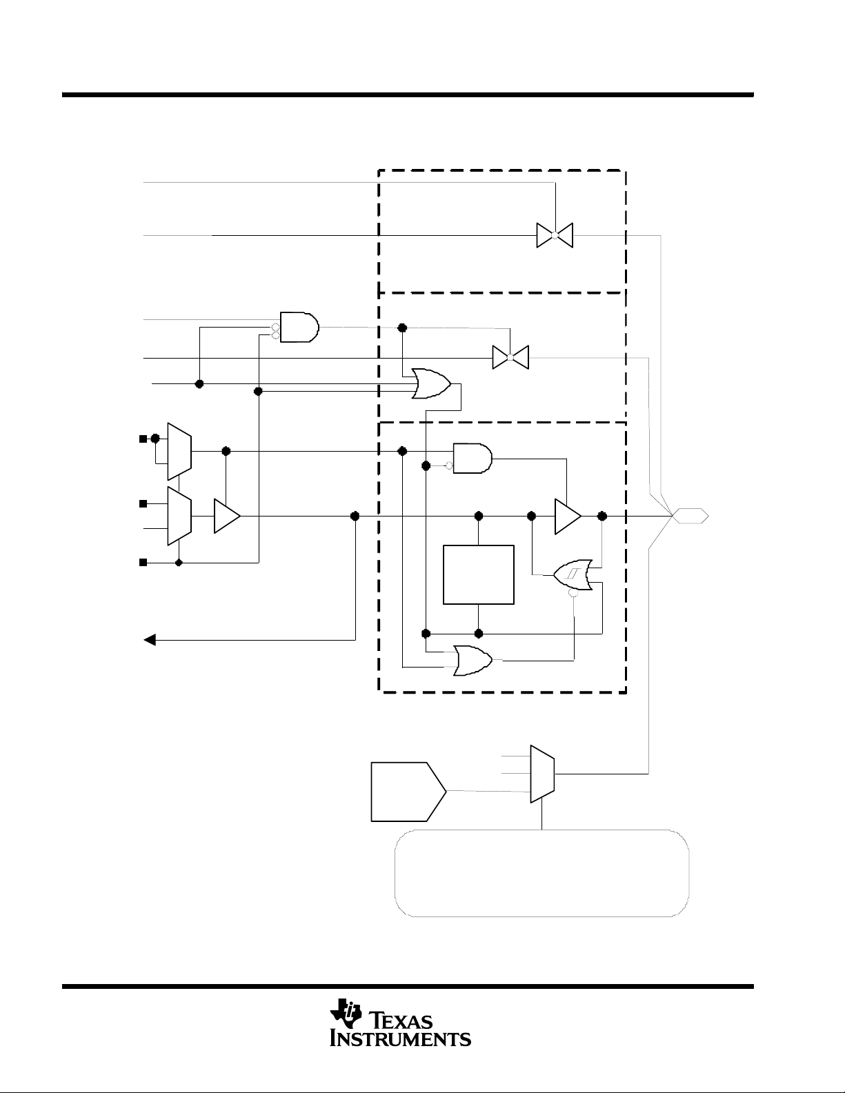
MSP430xG461x
MIXED SIGNAL MICROCONTROLLER
SLAS508G -- APRIL 2006 -- REVISED OCTOBER 2007
input/output schematic (continued)
port P5, P5.1, input/output with Schmitt-trigger
INCH=12
A12
LCDS0
Segment Sy
DAC12.1OPS
P5DIR.x
P5OUT.x
DV
P5SEL.x
SS
#
Pad Logic
#
0
1
Direction
0: Input
1: Output
0
1
Bus
P5.1/S0/A12/DAC1
Keeper
EN
P5IN.x
Note:x = 1
y=0
0
DAC1
DV
SS
1
2
0 if DAC12.1AMPx = 0 and DAC12.1OPS= 1
1 if DAC12.1AMPx = 1 and DAC12.1OPS= 1
2 if DAC12.1AMPx > 1 and DAC12.1OPS= 1
76
POST OFFICE BOX 655303 • DALLAS, TEXAS 75265
Page 77

Port P5 (P5.1) pin functions
X
///
PIN NAME (P5.X)
P5.1/S0/A12/DAC1 1
NOTES: 1. X: Don’t care.
2. Setting the P5SEL.x bit disables the output driver as well as the input Schmitt trigger to prevent parasitic cross currents when
applying analog signals.
P5.1 (I/O) (see Note 1) I: 0; O: 1 0 X 0 X 0
DAC1 high impedance
(see Note 1)
DVSS (see Note 1) X X X 1 1 X
DAC1 output
(see Note 1)
A12 (see Notes 1, 2) X 1 12 0 X 0
S0 enabled (see Note 1) X 0 X 0 X 1
S0 disabled
(see Note 1)
FUNCTION
MSP430xG461x
MIXED SIGNAL MICROCONTROLLER
SLAS508G -- APRIL 2006 -- REVISED OCTOBER 2007
CONTROL BITS / SIGNALS
P5DIR.x P5SEL.x INCHx DAC12.1OPS DAC12.1AMPx LCDS0
X X X 1 0 X
X X X 1 >1 X
X 1 X 0 X 1
POST OFFICE BOX 655303 • DALLAS, TEXAS 75265
77
Page 78

MSP430xG461x
X
/
/
/
MIXED SIGNAL MICROCONTROLLER
SLAS508G -- APRIL 2006 -- REVISED OCTOBER 2007
input/output schematic (continued)
port P5, P5.2 to P5.4, input/output with Schmitt-trigger
LCD Signal
DV
SS
Pad Logic
P5DIR.x
0
1
P5OUT .x
DV
SS
0
1
P5SEL.x
P5IN.x
Note: x = 2,3,4
Port P5 (P5.2 to P5.4) pin functions
PIN NAME (P5.X)
P5.2/COM1 2
P5.3/COM2 3
P5.4/COM3 4
NOTE 1: X: Don’t care.
P5.2 (I/O) I: 0; O: 1 0
COM1 (see Note 1) X 1
P5.3 (I/O) I: 0; O: 1 0
COM2 (see Note 1) X 1
P5.4 (I/O) I: 0; O: 1 0
COM3 (see Note 1) X 1
Direction
0: Input
1: Output
FUNCTION
Bus
Keeper
EN
P5.2/COM1
P5.3/COM2
P5.4/COM3
CONTROL BITS / SIGNALS
P5DIR.x P5SEL.x
78
POST OFFICE BOX 655303 • DALLAS, TEXAS 75265
Page 79

input/output schematic (continued)
X
/
/
/
/
port P5, P5.5 to P5.7, input/output with Schmitt-trigger
LCD Signal
DV
SS
MSP430xG461x
MIXED SIGNAL MICROCONTROLLER
SLAS508G -- APRIL 2006 -- REVISED OCTOBER 2007
Pad Logic
P5DIR.x
0
1
Direction
0: Input
1: Output
P5OUT .x
DV
SS
0
1
P5SEL.x
P5IN.x
Note: x = 5,6,7
Port P5 (P5.5 to P5.7) pin functions
PIN NAME (P5.X)
P5.5/R03 5
P5.6/LCDREF/R13 6
P5.7/R03 7
NOTES: 1. X: Don’t care.
2. External reference for the LCD_A charge pump is applied when VLCDREFx = 01. Otherwise R13 is selected.
P5.5 (I/O) I: 0; O: 1 0
R03(seeNote1) X 1
P5.6 (I/O) I: 0; O: 1 0
R13 or LCDREF (see Notes 1, 2) X 1
P5.7 (I/O) I: 0; O: 1 0
R03(seeNote1) X 1
FUNCTION
Bus
Keeper
EN
P5.5/R03
P5.6/LCDREF/R13
P5.7/R03
CONTROL BITS / SIGNALS
P5DIR.x P5SEL.x
POST OFFICE BOX 655303 • DALLAS, TEXAS 75265
79
Page 80

MSP430xG461x
/
/
/
/
/
/
MIXED SIGNAL MICROCONTROLLER
SLAS508G -- APRIL 2006 -- REVISED OCTOBER 2007
input/output schematic (continued)
port P6, P6.0, P6.2, and P6.4, input/output with Schmitt-trigger
Ay
#
#
0
INCH=0/2/4
P6DIR.x
1
P6OUT.x
DV
SS
0
1
P6SEL.x
P6IN.x
Note:x=0,2,4
y=0,1
# = Signal from or to ADC12
Direction
0: Input
1: Output
Pad Logic
P6.0/A0/OA0I0
P6.2/A2/OA0I1
P6.4/A4/OA1I0
Bus
Keeper
EN
Port P6 (P6.0, P6.2, and P6.4) pin functions
PIN NAME (P6.X)
P6.0/A0/OA0I0 0
P6.2/A2/OA0I1 2
P6.4/A4/OA1I0 4
NOTES: 1. X: Don’t care.
2. N/A: Not available or not applicable.
3. Setting the P6SEL.x bit disables the output driver as well as the input Schmitt trigger to prevent parasitic cross currents when
applying analog signals.
X FUNCTION
P6.0 (I/O) (see Note 1) I: 0; O: 1 0 X X X
OA0I0(seeNote1) 0 X 0 X X
A0 (see Notes 1, 3) X 1 X X 0
P6.2 (I/O) (see Note 1) I: 0; O: 1 0 X X X
OA0I1(seeNote1) 0 X 1 X X
A2 (see Notes 1, 3) X 1 X X 2
P6.4 (I/O) (see Note 1) I: 0; O: 1 0 X X X
OA1I0(seeNote1) 0 X X 0 X
A4 (see Notes 1, 3) X 1 X X 4
+
OA0/1
--
CONTROL BITS / SIGNALS
P6DIR.x P6SEL.x
OAPx (OA0)
OANx (OA0)
OAPx (OA1)
OANx(OA1)
INCHx
80
POST OFFICE BOX 655303 • DALLAS, TEXAS 75265
Page 81

input/output schematic (continued)
port P6, P6.1, P6.3, and P6.5 input/output with Schmitt-trigger
MSP430xG461x
MIXED SIGNAL MICROCONTROLLER
SLAS508G -- APRIL 2006 -- REVISED OCTOBER 2007
INCH=1/3/5
Ay
P6DIR.x
P6OUT.x
DV
P6SEL.x
P6IN.x
#
#
SS
Pad Logic
0
1
Direction
0: Input
1: Output
P6.1/A1/OA0O
P6.3/A3/OA1O
P6.5/A5/OA2O
0
1
Bus
Keeper
EN
OAPMx> 0
OAADC1
Note:x=1,3,5
y = 0, 1, 2
# = Signal from or to ADC12
+
OAy
--
POST OFFICE BOX 655303 • DALLAS, TEXAS 75265
81
Page 82

MSP430xG461x
X
/
/
/
/
/
/
MIXED SIGNAL MICROCONTROLLER
SLAS508G -- APRIL 2006 -- REVISED OCTOBER 2007
Port P6 (P6.1, P6.3, and P6.5) pin functions
PIN NAME (P6.X)
P6.1/A1/OA0O 1
P6.3/A3/OA1O 3
P6.5/A5/OA2O 5
NOTES: 1. X: Don’t care.
2. N/A: Not available or not applicable.
3. Setting the P6SEL.x bit disables the output driver as well as the input Schmitt trigger to prevent parasitic cross currents when
applying analog signals.
4. Setting the OAADC1 bit or setting OAFCx = 00 will cause the operational amplifier to be present at the pin as well as internally
connected to the corresponding ADC12 input.
FUNCTION
P6.1 (I/O) (see Note 1) I: 0; O: 1 0 X 0 X
OA0O (see Notes 1, 4) X X 1 >0 X
A1 (see Notes 1, 3) X 1 X 0 1
P6.3 (I/O) (see Note 1) I: 0; O: 1 0 X 0 X
OA1O (see Notes 1, 4) X X 1 >0 X
A3 (see Notes 1, 3) X 1 X 0 3
P6.5 (I/O) (see Note 1) I: 0; O: 1 0 X 0 X
OA2O (see Notes 1, 4) X X 1 >0 X
A5 (see Notes 1, 3) X 1 X 0 5
CONTROL BITS / SIGNALS
P6DIR.x P6SEL.x OAADC1 OAPMx INCHx
82
POST OFFICE BOX 655303 • DALLAS, TEXAS 75265
Page 83
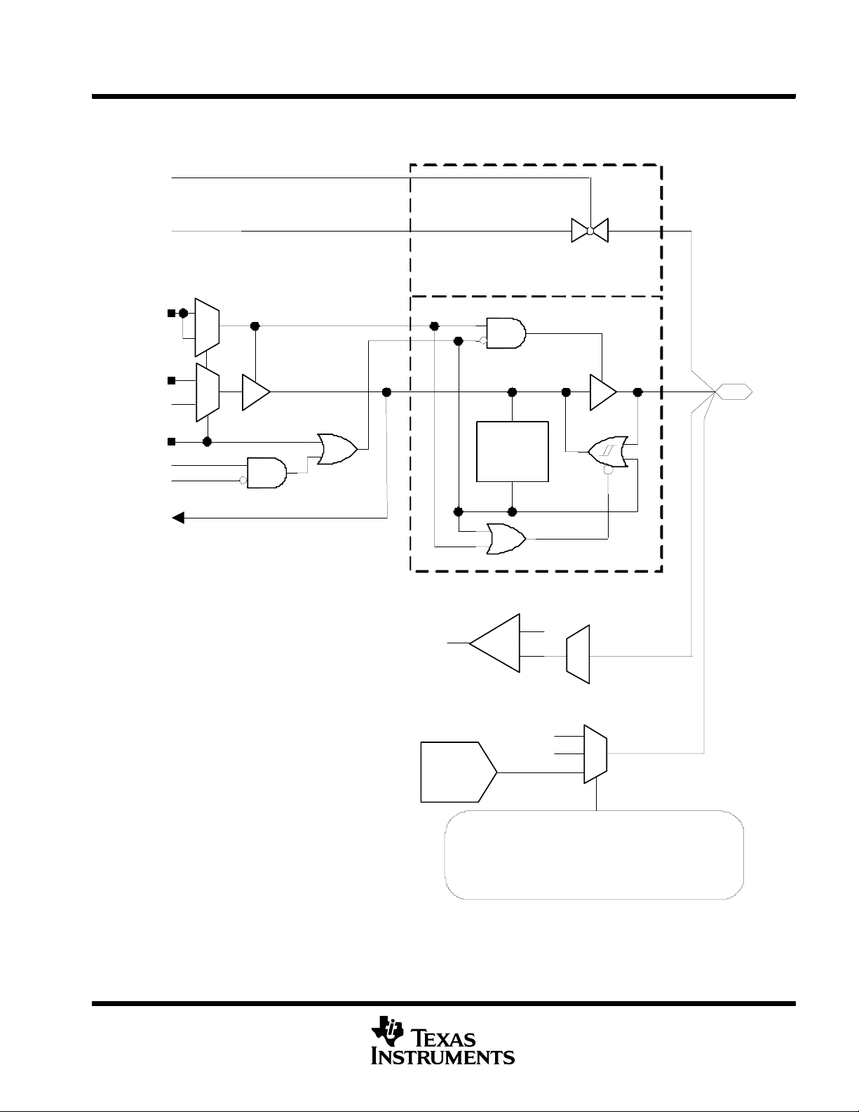
input/output schematic (continued)
port P6, P6.6, input/output with Schmitt-trigger
MSP430xG461x
MIXED SIGNAL MICROCONTROLLER
SLAS508G -- APRIL 2006 -- REVISED OCTOBER 2007
INCH=6
A6
P6DIR.x
P6OUT.x
DV
SS
P6SEL.x
DAC12.0AMP> 0
DAC12.0OPS
P6IN.x
#
Pad Logic
#
0
1
Direction
0: Input
1: Output
P6.6 /A6/DAC0/OA2I0
0
1
Bus
Keeper
EN
Note:x = 6
# = Signal from or to ADC12
+
OA2
--
0
DVSS
DAC0
1
2
0 if DAC12.0AMPx= 0 and DAC12.0OPS = 0
1 if DAC12.0AMPx= 1 and DAC12.0OPS = 0
2 if DAC12.0AMPx> 1 and DAC12.0OPS = 0
POST OFFICE BOX 655303 • DALLAS, TEXAS 75265
83
Page 84

MSP430xG461x
///
MIXED SIGNAL MICROCONTROLLER
SLAS508G -- APRIL 2006 -- REVISED OCTOBER 2007
Port P6 (P6.6) pin functions
PIN NAME (P6.X)
P6.6/A6/DAC0/OA2I0 6
NOTES: 1. X: Don’t care.
2. Setting the P6SEL.x bit disables the output driver as well as the input Schmitt trigger to prevent parasitic cross currents when
applying analog signals.
X FUNCTION
P6.6 (I/O) (see Note 1) I: 0; O: 1 0 X 1 X X
DAC0 high impedance
(see Note 1)
DVSS (see Note 1) X X X 0 1 X
DAC0 output
(see Note 1)
A6 (see Notes 1, 2) X 1 6 X X X
OA2I0(seeNote1) 0 X 0 X X 0
CONTROL BITS / SIGNALS
P6DIR.x P6SEL.x INCHx DAC12.0OPS DAC12.0AMPx
X X X 0 0 X
X X X 0 >1 X
OAPx (OA2)
OANx (OA2)
84
POST OFFICE BOX 655303 • DALLAS, TEXAS 75265
Page 85

input/output schematic (continued)
port P6, P6.7, input/output with Schmitt-trigger
To SVS Mux
MSP430xG461x
MIXED SIGNAL MICROCONTROLLER
SLAS508G -- APRIL 2006 -- REVISED OCTOBER 2007
INCH=7
A7
P6DIR.x
P6OUT.x
DV
SS
P6SEL.x
VLD =15
DAC12.1AMP> 0
DAC12.1OPS
#
Pad Logic
#
0
1
Direction
0: Input
1: Output
0
1
Bus
P6.7/A7/DAC1/SVSIN
Keeper
EN
P6IN.x
Note:x = 7
# = Signal from or to ADC12
0
DVSS
DAC1
1
2
0 if DAC12.1AMPx = 0 and DAC12.1OPS= 0
1 if DAC12.1AMPx = 1 and DAC12.1OPS= 0
2 if DAC12.1AMPx > 1 and DAC12.1OPS= 0
POST OFFICE BOX 655303 • DALLAS, TEXAS 75265
85
Page 86

MSP430xG461x
X
///
MIXED SIGNAL MICROCONTROLLER
SLAS508G -- APRIL 2006 -- REVISED OCTOBER 2007
Port P6 (P6.7) pin functions
PIN NAME (P6.X)
P6.7/A7/DAC1/SVSIN 7
NOTES: 1. X: Don’t care.
2. Setting the P6SEL.x bit disables the output driver as well as the input Schmitt trigger to prevent parasitic cross currents when
applying analog signals.
3. Setting VLDx = 15 will also cause the external SVSIN to be used. In this case, the P6SEL.x bit is a do not care.
FUNCTION
P6.7 (I/O) (see Note 1) I: 0; O: 1 0 X 1 X
DAC1 high impedance
(see Note 1)
DVSS (see Note 1) X X X 0 1
DAC1 output
(see Note 1)
A7 (see Notes 1, 2) X 1 7 X X
SVSIN (see Notes 1,3) 0 1 0 1 X
CONTROL BITS / SIGNALS
P6DIR.x P6SEL.x INCHx DAC12.1OPS DAC12.1AMPx
X X X 0 0
X X X 0 >1
86
POST OFFICE BOX 655303 • DALLAS, TEXAS 75265
Page 87

input/output schematic (continued)
port P7, P7.0 to P7.3, input/output with Schmitt-trigger
LCDS28/32
Segment Sy
DV
SS
MSP430xG461x
MIXED SIGNAL MICROCONTROLLER
SLAS508G -- APRIL 2006 -- REVISED OCTOBER 2007
Pad Logic
P7DIR.x
Direction control
from Module X
P7OUT.x
Module X OUT
P7SEL.x
P7IN.x
Module X IN
Note:x=0,1,2,3
y = 30, 31, 32, 33
0
1
Direction
0: Input
1: Output
0
1
Bus
Keeper
P7.3/UCA0CLK/S30
P7.2/UCA0SOMI/S31
P7.1/UCA0SIMO/S32
P7.0/UCA0STE/S33
EN
EN
D
POST OFFICE BOX 655303 • DALLAS, TEXAS 75265
87
Page 88

MSP430xG461x
X
/
/
/
/
/
/
/
/
MIXED SIGNAL MICROCONTROLLER
SLAS508G -- APRIL 2006 -- REVISED OCTOBER 2007
Port P7 (P7.0 to P7.1) pin functions
PIN NAME (P7.X)
P7.0/UCA0STE/S33 0
P7.1/UCA0SIMO/S32 1
P7.2/UCA0SOMI/S31 2
P7.3/UCA0CLK/S30 3
NOTES: 1. X: Don’t care.
2. The pin direction is controlled by the USCI module.
3. The pin direction is controlled by the USCI module.
P7.0 (I/O) I: 0; O: 1 0 0
USCI_A0.UCA0STE (see Notes 1, 2) X 1 0
S33(seeNote1) X X 1
P7.1 (I/O) I: 0; O: 1 0 0
USCI_A0.UCA0SIMO (see Notes 1, 2) X 1 0
S32(seeNote1) X X 1
P7.2 (I/O) I: 0; O: 1 0 0
USCI_A0.UCA0SOMI (see Notes 1, 3) X 1 0
S31(seeNote1) X X 1
P7.3 (I/O) I: 0; O: 1 0 0
USCI_A0.UCA0CLK (see Notes 1, 3) X 1 0
S30(seeNote1) X X 1
FUNCTION
CONTROL BITS / SIGNALS
P7DIR.x P7SEL.x LCDS32
88
POST OFFICE BOX 655303 • DALLAS, TEXAS 75265
Page 89
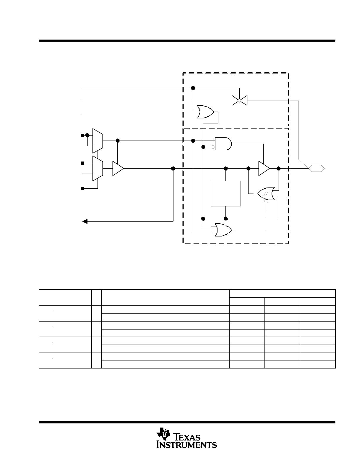
input/output schematic (continued)
X
/
/
/
/
port P7, P7.4 to P7.7, input/output with Schmitt-trigger
LCDS24/28
Segment Sy
DV
SS
MSP430xG461x
MIXED SIGNAL MICROCONTROLLER
SLAS508G -- APRIL 2006 -- REVISED OCTOBER 2007
Pad Logic
P7DIR.x
0
1
P7OUT .x
DV
SS
0
1
P7SEL.x
P7IN.x
Note:x=4,5,6,7
y = 26, 27, 28, 29
Port P7 (P7.4 to P7.5) pin functions
PIN NAME (P7.X)
P7.4/S29 4
P7.5/S28 5
P7.6/S27 6
P7.7/S26 7
NOTE 1: X: Don’t care.
P7.4 (I/O) I: 0; O: 1 0 0
S29(seeNote1) X X 1
P7.5 (I/O) I: 0; O: 1 0 0
S28(seeNote1) X X 1
P7.6 (I/O) I: 0; O: 1 0 0
S27(seeNote1) X X 1
P7.7 (I/O) I: 0; O: 1 0 0
S26(seeNote1) X X 1
Direction
0: Input
1: Output
FUNCTION
Bus
Keeper
EN
P7.7/S26
P7.6/S27
P7.5/S28
P7.4/S29
CONTROL BITS / SIGNALS
P7DIR.x P7SEL.x LCDS28
POST OFFICE BOX 655303 • DALLAS, TEXAS 75265
89
Page 90

MSP430xG461x
MIXED SIGNAL MICROCONTROLLER
SLAS508G -- APRIL 2006 -- REVISED OCTOBER 2007
input/output schematic (continued)
port P8, P8.0 to P8.7, input/output with Schmitt-trigger
LCDS16/20/24
Segment Sy
DV
SS
Pad Logic
P8DIR.x
0
1
P8OUT .x
DV
SS
0
1
P8SEL.x
P8IN.x
Note: x = 0,1,2,3,4,5,6,7
y= 25,24,23,22,21,20,19,18
Direction
0: Input
1: Output
Bus
Keeper
EN
P8.7/S18
P8.6/S19
P8.5/S20
P8.4/S21
P8.3/S22
P8.2/S23
P8.1/S24
P8.0/S25
90
POST OFFICE BOX 655303 • DALLAS, TEXAS 75265
Page 91

Port P8 (P8.0 to P8.1) pin functions
X
/
/
/
/
/
/
X
/
/
PIN NAME (P8.X)
P8.0/S18 0
P8.1/S19 0
P8.2/S20 2
P8.3/S21 3
P8.4/S22 4
P8.5/S23 5
NOTE 1: X: Don’t care.
P8.0 (I/O) I: 0; O: 1 0 0
S18(seeNote1) X X 1
P8.0 (I/O) I: 0; O: 1 0 0
S19(seeNote1) X X 1
P8.2 (I/O) I: 0; O: 1 0 0
S20(seeNote1) X X 1
P8.3 (I/O) I: 0; O: 1 0 0
S21(seeNote1) X X 1
P8.4 (I/O) I: 0; O: 1 0 0
S22(seeNote1) X X 1
P8.5 (I/O) I: 0; O: 1 0 0
S23(seeNote1) X X 1
Port P8 (P8.6 to P8.7) pin functions
PIN NAME (P8.X)
P8.6/S24 6
P8.7/S25 7
NOTE 1: X: Don’t care.
P8.6 (I/O) I: 0; O: 1 0 0
S24(seeNote1) X X 1
P8.7 (I/O) I: 0; O: 1 0 0
S25(seeNote1) X X 1
FUNCTION
FUNCTION
MSP430xG461x
MIXED SIGNAL MICROCONTROLLER
SLAS508G -- APRIL 2006 -- REVISED OCTOBER 2007
CONTROL BITS / SIGNALS
P8DIR.x P8SEL.x LCDS16
CONTROL BITS / SIGNALS
P8DIR.x P8SEL.x LCDS24
POST OFFICE BOX 655303 • DALLAS, TEXAS 75265
91
Page 92

MSP430xG461x
MIXED SIGNAL MICROCONTROLLER
SLAS508G -- APRIL 2006 -- REVISED OCTOBER 2007
input/output schematic (continued)
port P9, P9.0 to P9.7, input/output with Schmitt-trigger
LCDS8/12/16
Segment Sy
DV
SS
Pad Logic
P9DIR.x
0
1
P9OUT .x
DV
SS
0
1
P9SEL.x
P9IN.x
Note: x = 0,1,2,3,4,5,6,7
y= 17,16,15,14,13,12,11,10
Direction
0: Input
1: Output
Bus
Keeper
EN
P9.7/S10
P9.6/S11
P9.5/S12
P9.4/S13
P9.3/S14
P9.2/S15
P9.1/S16
P9.0/S17
92
POST OFFICE BOX 655303 • DALLAS, TEXAS 75265
Page 93

Port P9 (P9.0 to P9.1) pin functions
X
/
/
/
/
/
/
/
/
PIN NAME (P9.X)
P9.0/S17 0
P9.1/S16 1
P9.2/S20 2
P9.3/S21 3
P9.4/S22 4
P9.5/S23 5
P9.6/S24 6
P9.7/S25 7
NOTE 1: X: Don’t care.
P9.0 (I/O) I: 0; O: 1 0 0
S17(seeNote1) X X 1
P9.1 (I/O) I: 0; O: 1 0 0
S16(seeNote1) X X 1
P9.2 (I/O) I: 0; O: 1 0 0
S15(seeNote1) X X 1
P9.3 (I/O) I: 0; O: 1 0 0
S14(seeNote1) X X 1
P9.4 (I/O) I: 0; O: 1 0 0
S13(seeNote1) X X 1
P9.5 (I/O) I: 0; O: 1 0 0
S12(seeNote1) X X 1
P9.6 (I/O) I: 0; O: 1 0 0
S11(seeNote1) X X 1
P9.7 (I/O) I: 0; O: 1 0 0
S10(seeNote1) X X 1
FUNCTION
MSP430xG461x
MIXED SIGNAL MICROCONTROLLER
SLAS508G -- APRIL 2006 -- REVISED OCTOBER 2007
CONTROL BITS / SIGNALS
P9DIR.x P9SEL.x LCDS16
POST OFFICE BOX 655303 • DALLAS, TEXAS 75265
93
Page 94

MSP430xG461x
X
/
/
/
/
/
/
MIXED SIGNAL MICROCONTROLLER
SLAS508G -- APRIL 2006 -- REVISED OCTOBER 2007
input/output schematic (continued)
port P10, P10.0 to P10.5, input/output with Schmitt-trigger
LCDS4/8
Segment Sy
DV
SS
Pad Logic
P10DIR.x
0
1
Direction
0: Input
1: Output
P10OUT.x
DV
SS
0
1
P10SEL.x
P10IN.x
Note: x = 0,1,2,3,4,5
y = 9,8,7,6,5,4
Port P10 (P10.0 to P10.1) pin functions
PIN NAME (P10.X)
P10.0/S8 0
P10.1/S7 1
P10.2/S7 2
P10.3/S6 3
P10.4/S5 4
P10.5/S4 5
NOTE 1: X: Don’t care.
P10.0 (I/O) I: 0; O: 1 0 0
S8 (see Note 1) X X 1
P10.1 (I/O) I: 0; O: 1 0 0
S7 (see Note 1) X X 1
P10.2 (I/O) I: 0; O: 1 0 0
S7 (see Note 1) X X 1
P10.3 (I/O) I: 0; O: 1 0 0
S6 (see Note 1) X X 1
P10.4 (I/O) I: 0; O: 1 0 0
S5 (see Note 1) X X 1
P10.5 (I/O) I: 0; O: 1 0 0
S4 (see Note 1) X X 1
FUNCTION
Bus
Keeper
EN
P10.5/S4
P10.4/S5
P10.3/S6
P10.2/S7
P10.1/S8
P10.0/S9
CONTROL BITS / SIGNALS
P10DIR.x P10SEL.x LCDS8
94
POST OFFICE BOX 655303 • DALLAS, TEXAS 75265
Page 95

input/output schematic (continued)
X
/
/
port P10, P10.6, input/output with Schmitt-trigger
MSP430xG461x
MIXED SIGNAL MICROCONTROLLER
SLAS508G -- APRIL 2006 -- REVISED OCTOBER 2007
INCH=15
A15
LCDS0
Segment Sy
P10DIR.x
P10OUT.x
DV
SS
P10SEL.x
#
Pad Logic
#
0
1
Direction
0: Input
1: Output
0
1
P10.6/S3/A15
Bus
Keeper
EN
P10IN.x
Note: x = 6
=3
y
Port P10 (P10.6) pin functions
PIN NAME (P10.X)
P10.6/S3/A15 6
NOTES: 1. X: Don’t care.
2. N/A: Not available or not applicable.
3. Setting the P10SEL.x bit disables the output driver as well as the input Schmitt trigger to prevent parasitic cross currents when
applying analog signals.
P5.0 (I/O) (see Note 1) I: 0; O: 1 0 X 0
A15 (see Notes 1, 3) X 1 15 0
S3 enabled (see Note 1) X 0 X 1
S3 disabled (see Note 1) X 1 X 1
FUNCTION
CONTROL BITS / SIGNALS
P10DIR.x P10SEL.x INCHx LCDS0
POST OFFICE BOX 655303 • DALLAS, TEXAS 75265
95
Page 96

MSP430xG461x
MIXED SIGNAL MICROCONTROLLER
SLAS508G -- APRIL 2006 -- REVISED OCTOBER 2007
input/output schematic (continued)
port P10, P10.7, input/output with Schmitt-trigger
INCH=14
A14
LCDS0
Segment Sy
P10DIR.x
P10OUT.x
DV
SS
P10SEL.x
#
Pad Logic
#
0
1
Direction
0: Input
1: Output
0
1
Bus
P10.7/S2/A14/OA2I1
Keeper
EN
P10IN.x
Note: x = 7
y= 2
+
OA2
--
96
POST OFFICE BOX 655303 • DALLAS, TEXAS 75265
Page 97

Port P10 (P10.7) pin functions
///
PIN NAME (P10.X)
P10.7/S2/A14/OA2I1 7
NOTES: 1. X: Don’t care.
2. N/A: Not available or not applicable.
3. Setting the P10SEL.x bit disables the output driver as well as the input Schmitt trigger to prevent parasitic cross currents when
applying analog signals.
X FUNCTION
P10.7(I/O)(seeNote1) I: 0; O: 1 0 X X 0
A14 (see Notes 1, 3) X 1 14 X 0
OA2I1 (see Notes 1, 3) 0 X X 1 0
S2 enabled (see Note 1) X 0 X X 1
S2 disabled (see Note 1) X 1 X X 1
MIXED SIGNAL MICROCONTROLLER
SLAS508G -- APRIL 2006 -- REVISED OCTOBER 2007
CONTROL BITS / SIGNALS
P10DIR.x P10SEL.x INCHx
MSP430xG461x
OAPx (OA1)
OANx (OA1)
LCDS0
POST OFFICE BOX 655303 • DALLAS, TEXAS 75265
97
Page 98

MSP430xG461x
MIXED SIGNAL MICROCONTROLLER
SLAS508G -- APRIL 2006 -- REVISED OCTOBER 2007
input/output schematic (continued)
Ve
#
/DAC0
REF+
DAC12.0OPS
DAC0_2_OA
Reference Voltage to DAC1
Reference Voltage to ADC12
Reference Voltage to DAC0
’0’, if DAC12CALON = 0
DAC12AMPx>1 AND DAC12OPS=1
+
’1’, if DAC12AMPx>1
’1’, if DAC12AMPx=1
DAC12OPS
If the reference of DAC0 is taken from pin Ve
In this situation, the DAC0 output is fed back to its own reference input.
1
0
--
REF+
0
1
#
/DAC0, unpredictable voltage levels will be on pin.
P6.6/A6/DAC0/OA2I0
Ve
/DAC0
REF+
98
POST OFFICE BOX 655303 • DALLAS, TEXAS 75265
Page 99

MSP430xG461x
MIXED SIGNAL MICROCONTROLLER
SLAS508G -- APRIL 2006 -- REVISED OCTOBER 2007
input/output schematic (continued)
JTAG pins TMS, TCK, TDI/TCLK, TDO/TDI, input/output with Schmitt-trigger or output
TDO
Controlled by JTAG
Controlled by JTAG
JTAG
Controlled
by JTAG
TDI
DV
CC
Burn and Test
TDO/TDI
Fuse
Test
and
Emulation
Module
TMS
TCK
TCK
Tau ~ 50 ns
Brownout
TDI/TCLK
DV
CC
TMS
DV
CC
TCK
RST/NMI
D
G
G
U
S
D
U
S
POST OFFICE BOX 655303 • DALLAS, TEXAS 75265
99
Page 100

MSP430xG461x
MIXED SIGNAL MICROCONTROLLER
SLAS508G -- APRIL 2006 -- REVISED OCTOBER 2007
JTAG fuse check mode
MSP430 devices that have the fuse on the TDI/TCLK terminal have a fuse check mode that tests the continuity
of the fuse the first time the JTAG port is accessed after a power-on reset (POR). When activated, a fuse check
current (I
taken to avoid accidentally activating the fuse check mode and increasing overall system power consumption.
Activation of the fuse check mode occurs with the first negative edge on the TMS pin after power up or if the
TMS is being held low during power up. The second positive edge on the TMS pin deactivates the fuse check
mode. After deactivation, the fuse check mode remains inactive until another POR occurs. After each POR the
fuse check mode has the potential to be activated.
The fuse check current only flows when the fuse check mode is active and the TMS pin is in a low state (see
Figure 37). Therefore, the additional current flow can be prevented by holding the TMS pin high (default
condition). The JTAG pins are terminated internally and therefore do not require external termination.
) of 1 mA at 3 V can flow from the TDI/TCLK pin to ground if the fuse is not burned. Care must be
(TF)
Time TMS Goes Low After POR
TMS
I
(TF)
I
TDI/TCLK
Figure 37. Fuse Check Mode Current
100
POST OFFICE BOX 655303 • DALLAS, TEXAS 75265
 Loading...