

Page 1

MSP430x241x, MSP430x261x
http://www.xinpian.net
提供单片机解密、IC解密、芯片解密业务
010-62245566 13810019655
MIXED SIGNAL MICROCONTROLLER
SLAS541A -- JUNE 2007 -- REVISED OCTOBER 2007
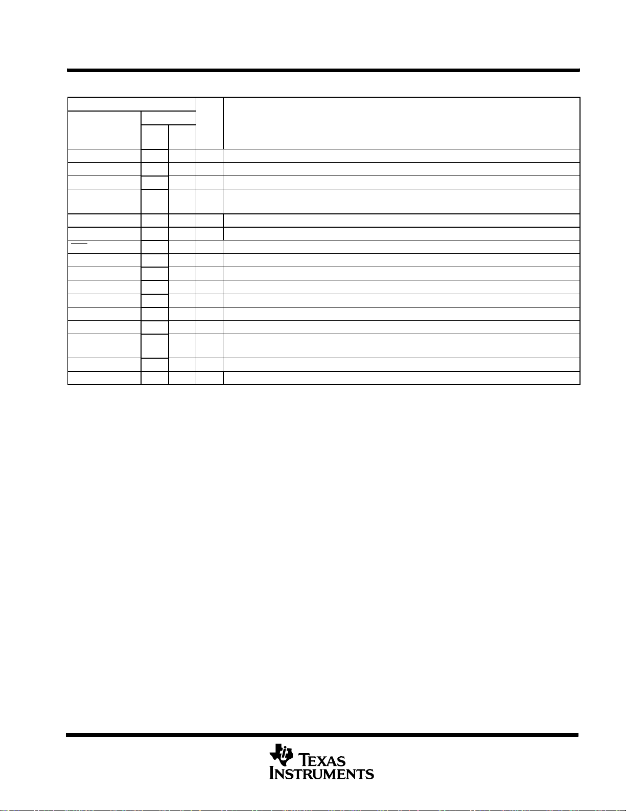
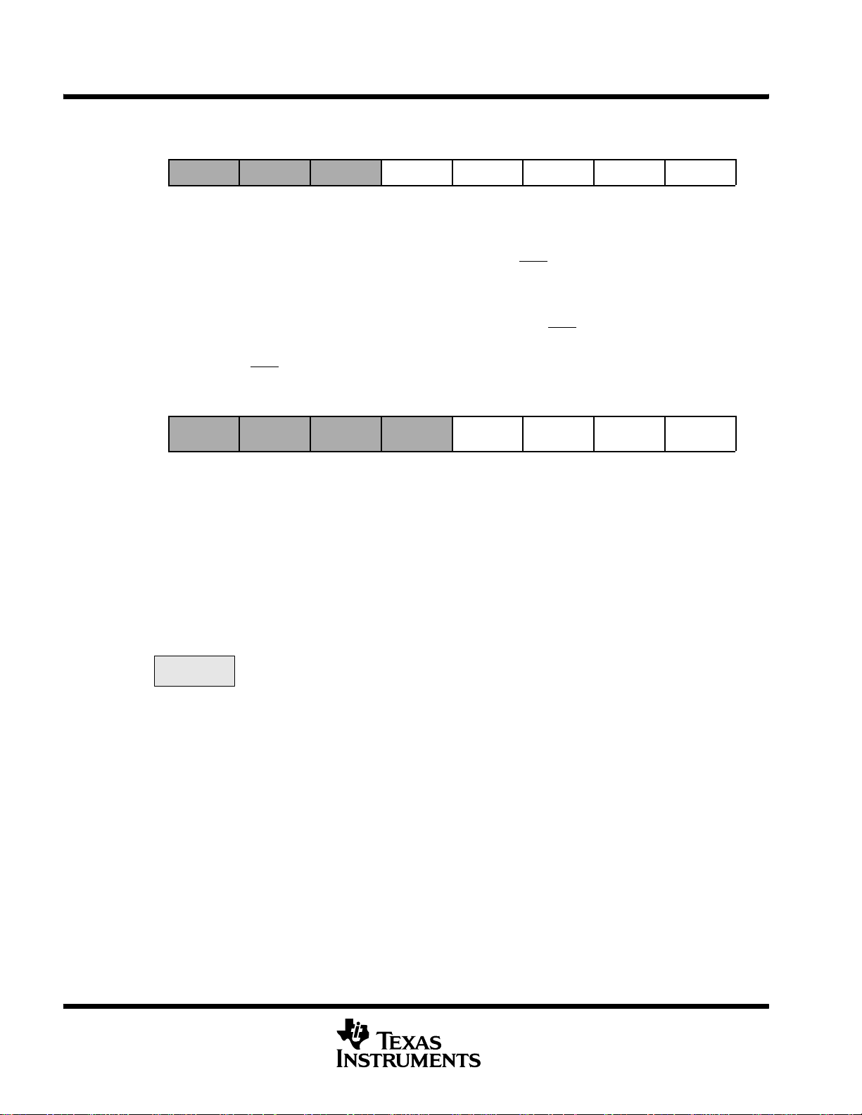
D Low Supply-Voltage Range, 1.8 V to 3.6 V
D Ultralow-Power Consumption:
-- Active Mode: 365 μAat1MHz,2.2V
-- Standby Mode (VLO): 0.5 μA
-- Off Mode (RAM Retention): 0.1 μA
D Wake-Up From Standby Mode in Less
Than 1 μs
D 16-Bit RISC Architecture,
62.5-nsInstruction Cycle Time
D Three-Channel Internal DMA
D 12-Bit Analog-to-Digital (A/D) Converter
With Internal Reference, Sample-and-Hold,
and Autoscan Feature
D Dual 12-Bit Digital-to-Analog (D/A)
Converters With Synchronization
D 16-Bit Timer_A With Three
Capture/Compare Registers
D 16-Bit Timer_B With Seven
Capture/Compare-With-Shadow Registers
D On-Chip Comparator
D Four Universal Serial Communication
Interfaces (USCIs)
-- USCI_A0 and USCI_A1
-- Enhanced UART Supporting
Auto-Baudrate Detection
-- IrDA Encoder and Decoder
-- Synchronous SPI
-- USCI_B0 and USCI_B1
2
Ct
-- I
-- Synchronous SPI
description
D Supply Voltage Supervisor/Monitor With
Programmable Level Detection
D Brownout Detector
D Bootstrap Loader
D Serial Onboard Programming,
No External Programming Voltage Needed
Programmable Code Protection by Security
Fuse
D Family Members Include:
-- MSP430F2416:
92KB+256B Flash Memory, 4KB RAM
-- MSP430F2417:
92KB+256B Flash Memory, 8KB RAM
-- MSP430F2418:
116KB+256B Flash Memory, 8KB RAM
-- MSP430F2419:
120KB+256B Flash Memory, 4KB RAM
-- MSP430F2616:
92KB+256B Flash Memory, 4KB RAM
-- MSP430F2617:
92KB+256B Flash Memory, 8KB RAM
-- MSP430F2618:
116KB+256B Flash Memory, 8KB RAM
-- MSP430F2619:
120KB+256B Flash Memory, 4KB RAM
D Availablein80-PinQuadFlatPack(QFP)
and 64-Pin QFP (See Available Options)
D For Complete Module Descriptions, See the
MSP430x2xx Family User’s Guide,
Literature Number SLAU144
†
The MSP430F241x devices are identical to the MSP430F261x
devices, with the exception that the DAC12 modules and the DMA
controller are not implemented.
The Texas Instruments MSP430 family of ultralow-power microcontrollers consists of several devices featuring
different sets of peripherals targeted for various applications. The architecture, combined with five low-power
modes is optimized to achieve extended battery life in por table measurement applications. The device features
a powerful 16-bit RISC CPU, 16-bit registers, and constant generators that contribute to maximum code
efficiency. The calibrated digitally controlled oscillator (DCO) allows wake-up from low-power modes to active
mode in less than 1 μs.
The MSP430F261x/241x series are microcontroller configurations with two built-in 16-bit timers, a fast 12-bit
A/D converter, a comparator, dual 12-bit D/A converters, four universal serial communication interface (USCI)
modules, DMA, and up to 64 I/O pins. The MSP430F241x devices are identical to the MSP430F261x devices,
with the exception that the DAC12 and the DMA modules are not implemented.
Typical applications include sensor systems, industrial control applications, hand-held meters, etc.
Please be aware that an important notice concerning availability, standard warranty, and use in critical applications of
Texas Instruments semiconductor products and disclaimers thereto appears at the end of this data sheet.
I2C is a registered trademark of Philips Incorporated.
PRODUCTION DATA information is current as of publication date.
Products conform to specifications per the terms of Texas Instruments
standard warranty. Production processing does not necessarily include
testing of all parameters.
POST OFFICE BOX 655303 • DALLAS, TEXAS 75265
Copyright © 2007, Texas Instruments Incorporated
1
Page 2
MSP430x241x, MSP430x261x
http://www.xinpian.net
提供单片机解密、IC解密、芯片解密业务
010-62245566 13810019655
MIXED SIGNAL MICROCONTROLLER
SLAS541A -- JUNE 2007 -- REVISED OCTOBER 2007
T
A
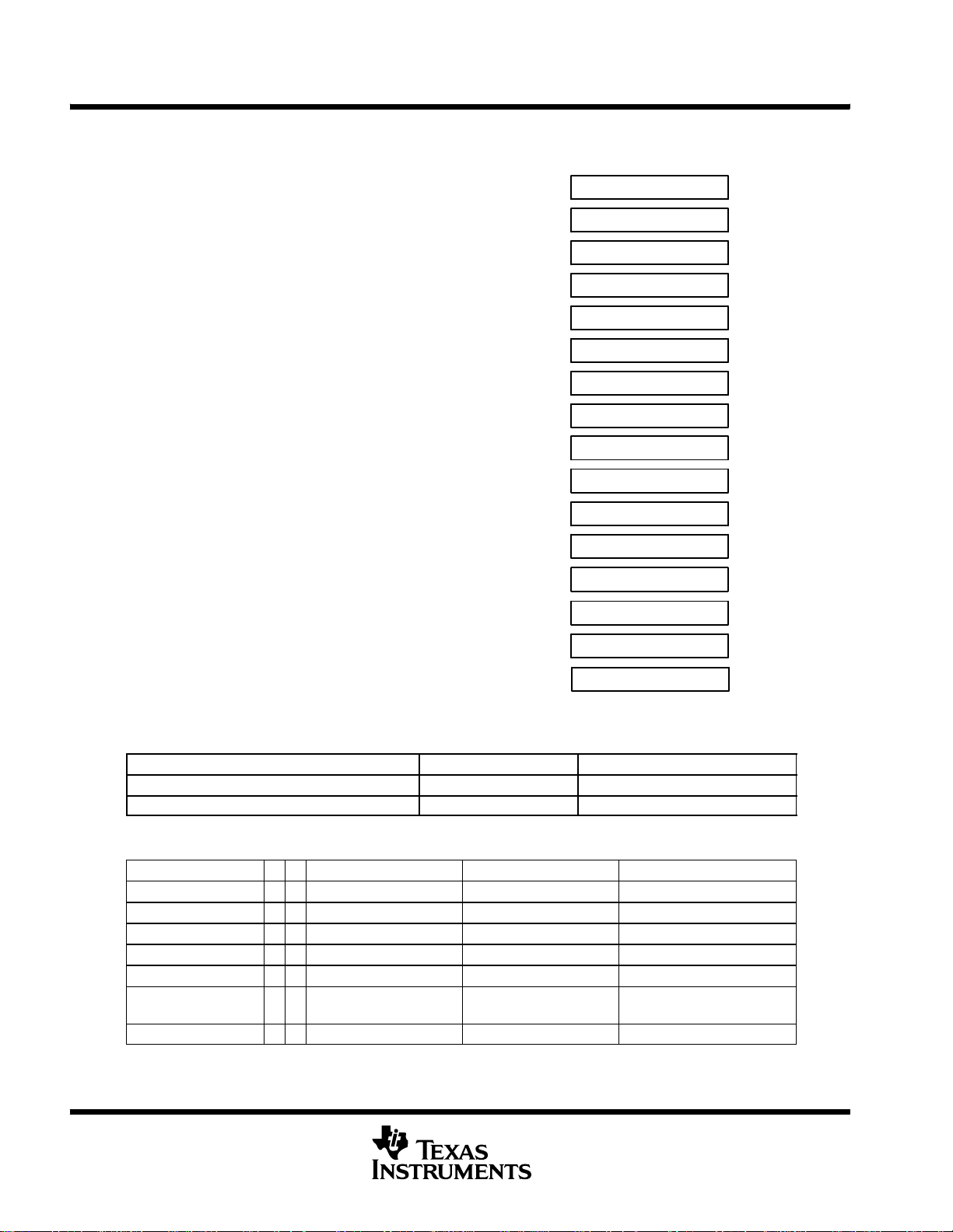
-- 4 0 °C to 105°C
PLASTIC 80-PIN LQFP (PN) PLASTIC 64-PIN LQFP (PM)
MSP430F2416TPN
MSP430F2417TPN
MSP430F2418TPN
MSP430F2419TPN
MSP430F2616TPN
MSP430F2617TPN
MSP430F2618TPN
MSP430F2619TPN
AVAILABLE OPTIONS
PACKAGED DEVICES
MSP430F2416TPM
MSP430F2417TPM
MSP430F2418TPM
MSP430F2419TPM
MSP430F2616TPM
MSP430F2617TPM
MSP430F2618TPM
MSP430F2619TPM
2
POST OFFICE BOX 655303 • DALLAS, TEXAS 75265
Page 3

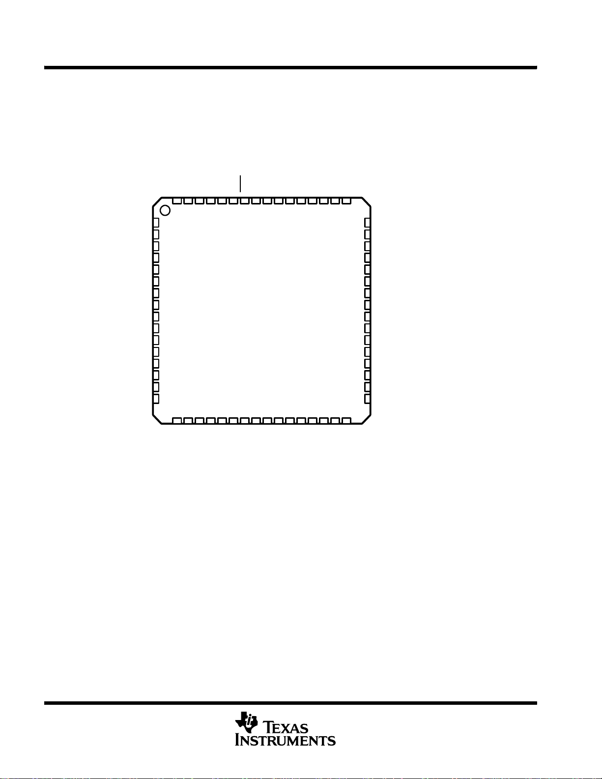
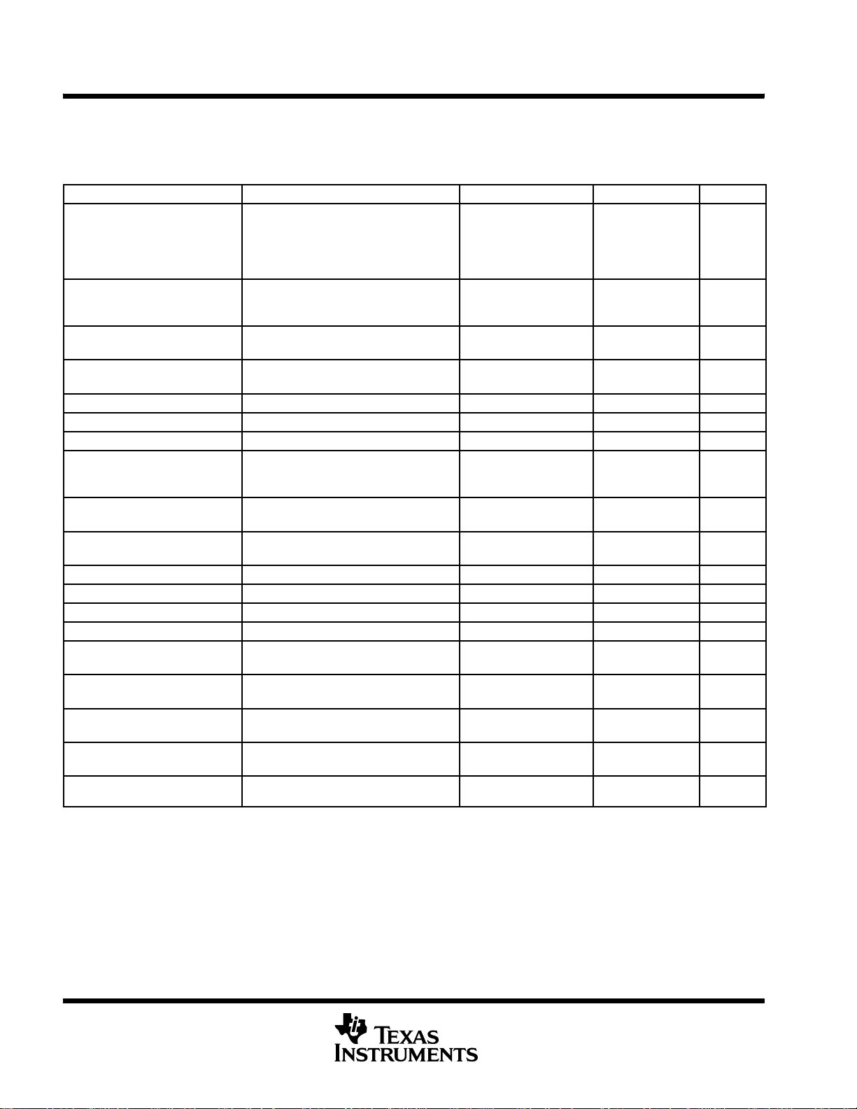
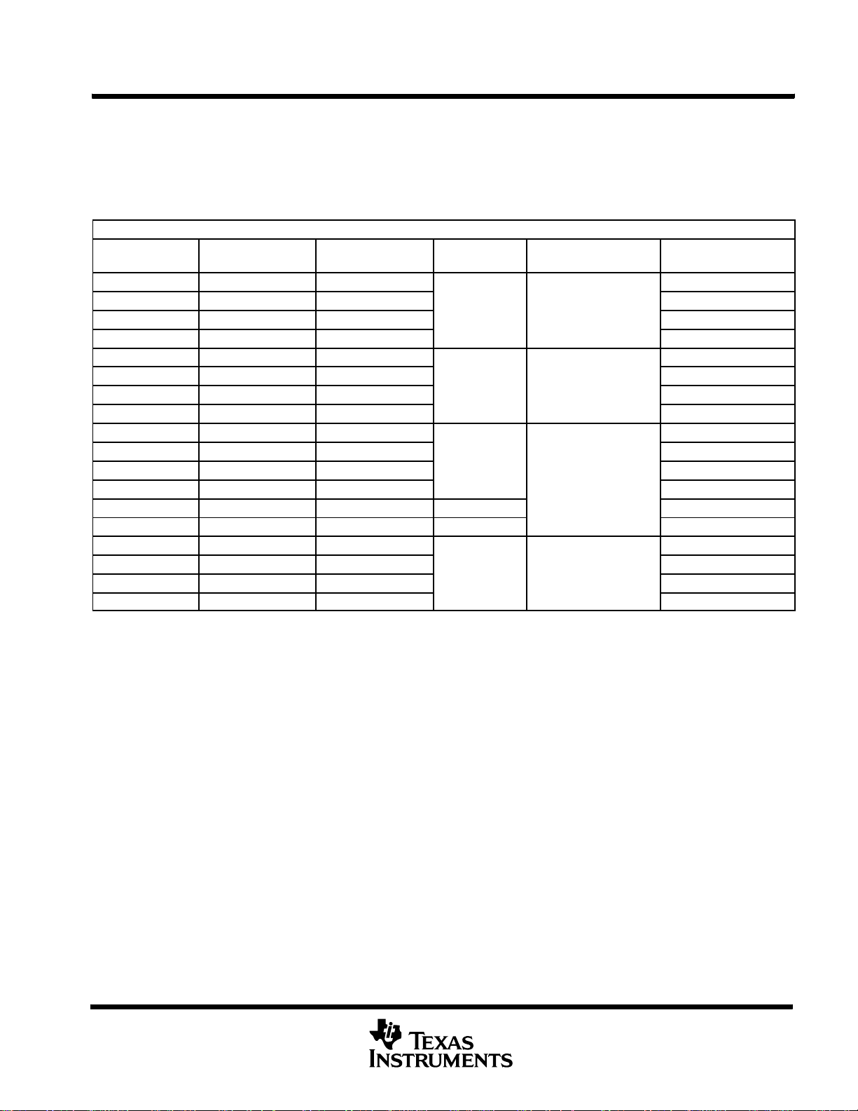
pin designation, MSP430F241x, 80-pin package
http://www.xinpian.net
提供单片机解密、IC解密、芯片解密业务
010-62245566 13810019655
SS1
AVSSP6.2/A2
P6.1/A1
P6.0/A0
RST/NMI
TCK
TMS
AVCCDV
TDI/TCLK
MSP430x241x, MSP430x261x
MIXED SIGNAL MICROCONTROLLER
SLAS541A -- JUNE 2007 -- REVISED OCTOBER 2007
TDO/TDI
P8.7/XT2IN
P8.5
P8.6/XT2OUT
P8.2
P8.3
P8.4
P7.7
P8.0
P8.1
DV
CC1
P6.3/A3
P6.4/A4
P6.5/A5
P6.6/A6
P6.7/A7/SVSIN
V
REF+
XIN
XOUT
Ve
REF+
V
/Ve
REF-
REF-
P1.0/TACLK/CAOUT
P1.1/TA0
P1.2/TA1
P1.3/TA2
P1.4/SMCLK
P1.5/TA0
P1.6/TA1
P1.7/TA2
P2.0/ACLK/CA2
78 77 76 75 74 73 72 71 70 69 68 67 66 65
80 79
1
2
3
4
5
6
7
8
9
10
11
12
80-pin
PN PACKAGE
(TOP VIEW)
13
14
15
16
17
18
19
20
21 22 23 24 25 26 27 28 29 30 31 32 33 34 35 36
/CA5
OSC
P2.7/TA0/CA7
P2.5/R
P2.6/ADC12CLK/CA6
P3.0/UCB0STE/UCA0CLK
P3.3/UCB0CLK/UCA0STE
P3.2/UCB0SOMI/UCB0SCL
P3.1/UCB0SIMO/UCB0SDA
P3.4/UCA0TXD/UCA0SIMO
P3.5/UCA0RXD/UCA0SOMI
P2.1/TAINCLK/CA3
P2.2/CAOUT/TA0/CA4
P2.3/CA0/TA1
P2.4/CA1/TA2
P3.6/UCA1TXD/UCA1SIMO
P3.7/UCA1RXD/UCA1SOMI
64
37
P4.0/TB0
63 62 61
38 39 40
P4.1/TB1
P4.2/TB2
P4.3/TB3
60
P7.6
59
P7.5
58
P7.4
57
P7.3
56
P7.2
55
P7.1
54
P7.0
53
DV
SS2
52
DV
CC2
51
P5.7/TBOUTH/SVSOUT
50
P5.6/ACLK
49
P5.5/SMCLK
48
P5.4/MCLK
47
P5.3/UCB1CLK/UCA1STE
46
P5.2/UCB1SOMI/UCB1SCL
45
P5.1/UCB1SIMO/UCB1SDA
44
P5.0/UCB1STE/UCA1CLK
43
P4.7/TBCLK
42
P4.6/TB6
P4.5/TB5
41
P4.4/TB4
POST OFFICE BOX 655303 • DALLAS, TEXAS 75265
3
Page 4
MSP430x241x, MSP430x261x
http://www.xinpian.net
提供单片机解密、IC解密、芯片解密业务
010-62245566 13810019655
MIXED SIGNAL MICROCONTROLLER
SLAS541A -- JUNE 2007 -- REVISED OCTOBER 2007
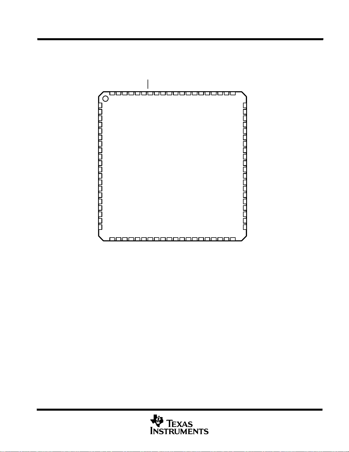
pin designation, MSP430F241x, 64-pin package
SS1
AVSSP6.2/A2
P6.1/A1
P6.0/A0
RST/NMI
TCK
TMS
64-pin
(TOP VIEW)
DV
CC1
P6.3/A3
P6.4/A4
P6.5/A5
P6.6/A6
P6.7/A7/SVSIN
V
REF+
XIN
XOUT
Ve
REF+
V
/Ve
REF-
REF-
P1.0/TACLK/CAOUT
P1.1/TA0
P1.2/TA1
P1.3/TA2
P1.4/SMCLK
AVCCDV
64 63
62 61 60 59 58 57 56 55 54 53 52 51 50 49
1
2
3
4
5
6
7
8
9
PM PACKAGE
10
11
12
13
14
15
16
17 18 19 20 21 22 23 24 25 26 27 28 29 30 31 32
TDI/TCLK
TDO/TDI
XT2IN
XT2OUT
P5.5/SMCLK
P5.7/TBOUTH/SVSOUT
P5.6/ACLK
48
P5.4/MCLK
47
P5.3/UC B1CLK/UCA1 STE
46
P5.2/UCB1SOMI/UCB1SCL
45
P5.1/UC B1SIMO/UCB 1 SDA
44
P5.0/UC B1STE/UCA1 CLK
43
P4.7/TBCLK
42
P4.6/TB6
41
P4.5/TB5
40
P4.4/TB4
39
P4.3/TB3
38
P4.2/TB2
37
P4.1/TB1
36
P4.0/TB0
35
P3.7/UC A1RXD/UCA1SOMI
34
P3.6/UC A1TXD/UCA1 SIMO
33
P3.5/UC A0RXD/UCA0SOMI
/CA5
P2.3/CA0/TA1
P2.4/CA1/TA2
OSC
P2.7/TA0/CA7
P2.5/R
P2.6/ADC12CLK/CA6
P3.0/UCB0STE/UCA0CLK
P3.3/UCB0CLK/UCA0STE
P3.2/UCB0SOMI/UCB0SCL
P3.1/UCB0SIMO/UCB0SDA
P3.4/UCA0TXD/UCA0SIMO
P1.5/TA0
P1.6/TA1
P1.7/TA2
P2.0/ACLK/CA2
P2.1/TAINCLK/CA3
P2.2/CAOUT/TA0/CA4
4
POST OFFICE BOX 655303 • DALLAS, TEXAS 75265
Page 5
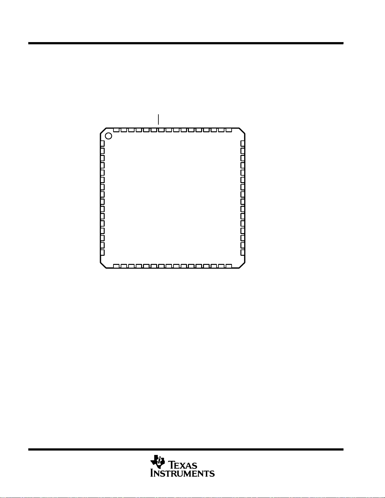
pin designation, MSP430F261x, 80-pin package
http://www.xinpian.net
提供单片机解密、IC解密、芯片解密业务
010-62245566 13810019655
SS1
AVSSP6.2/A2
P6.1/A1
P6.0/A0
RST/NMI
TCK
TMS
AVCCDV
TDI/TCLK
MSP430x241x, MSP430x261x
MIXED SIGNAL MICROCONTROLLER
SLAS541A -- JUNE 2007 -- REVISED OCTOBER 2007
TDO/TDI
P8.5
P8.6/XT2OUT
P8.7/XT2IN
P8.2
P8.3
P8.4
P7.7
P8.0
P8.1
DV
CC1
P6.3/A3
P6.4/A4
P6.5/A5/DAC1
P6.6/A6/DAC0
P6.7/A7/DAC1/SVSIN
V
REF+
XIN
XOUT
Ve
/DAC0
REF+
V
/Ve
REF-
REF-
P1.0/TACLK/CAOUT
P1.1/TA0
P1.2/TA1
P1.3/TA2
P1.4/SMCLK
P1.5/TA0
P1.6/TA1
P1.7/TA2
P2.0/ACLK/CA2
80 79
78 77 76 75 74 73 72 71 70 69 68 67 66 65
1
2
3
4
5
6
7
8
9
10
11
12
80-pin
PN PACKAGE
(TOP VIEW)
13
14
15
16
17
18
19
20
21 22 23 24 25 26 27 28 29 30 31 32 33 34 35 36
/CA5
OSC
P2.3/CA0/TA1
P2.4/CA1/TA2
P2.7/TA0/CA7
P2.5/R
P2.1/TAINCLK/CA3
P2.2/CAOUT/TA0/CA4
P3.0/UCB0STE/UCA0CLK
P2.6/ADC12CLK/DMAE0/CA6
P3.3/UCB0CLK/UCA0STE
P3.2/UCB0SOMI/UCB0SCL
P3.1/UCB0SIMO/UCB0SDA
P3.4/UCA0TXD/UCA0SIMO
P3.5/UCA0RXD/UCA0SOMI
P3.6/UCA1TXD/UCA1SIMO
P3.7/UCA1RXD/UCA1SOMI
64
37
P4.0/TB0
63 62 61
38 39 40
P4.1/TB1
P4.2/TB2
60
P7.6
59
P7.5
58
P7.4
57
P7.3
56
P7.2
55
P7.1
54
P7.0
53
DV
SS2
52
DV
CC2
51
P5.7/TBOUTH/SVSOUT
50
P5.6/ACLK
49
P5.5/SMCLK
48
P5.4/MCLK
47
P5.3/UCB1CLK/UCA1STE
46
P5.2/UCB1SOMI/UCB1SCL
45
P5.1/UCB1SIMO/UCB1SDA
44
P5.0/UCB1STE/UCA1CLK
43
P4.7/TBCLK
42
P4.6/TB6
P4.5/TB5
41
P4.3/TB3
P4.4/TB4
POST OFFICE BOX 655303 • DALLAS, TEXAS 75265
5
Page 6
MSP430x241x, MSP430x261x
http://www.xinpian.net
提供单片机解密、IC解密、芯片解密业务
010-62245566 13810019655
MIXED SIGNAL MICROCONTROLLER
SLAS541A -- JUNE 2007 -- REVISED OCTOBER 2007
pin designation, MSP430F261x, 64-pin package
SS1
AVSSP6.2/A2
P6.1/A1
P6.0/A0
RST/NMI
TCK
TMS
64-pin
(TOP VIEW)
DV
CC1
P6.3/A3
P6.4/A4
P6.5/A5/DAC1
P6.6/A6/DAC0
P6.7/A7/DAC1/SVSIN
V
REF+
XIN
XOUT
Ve
/DAC0
REF+
V
/Ve
REF-
REF-
P1.0/TACLK/CAOUT
P1.1/TA0
P1.2/TA1
P1.3/TA2
P1.4/SMCLK
AVCCDV
64 63
62 61 60 59 58 57 56 55 54 53 52 51 50 49
1
2
3
4
5
6
7
8
9
10
11
12
13
14
15
16
17 18 19 20 21 22 23 24 25 26 27 28 29 30 31 32
PM PACKA GE
TDI/TCLK
TDO/TDI
XT2IN
XT2OUT
P5.5/SMCLK
P5.7/TBOUTH/SVSOUT
P5.6/ACLK
48
P5.4/MCLK
47
P5.3/UCB1CLK/UCA1STE
46
P5.2/UCB1SOMI/UCB1SCL
45
P5.1/UCB1SIMO/UCB1SDA
44
P5.0/UCB1STE/UCA1CLK
43
P4.7/TBCLK
42
P4.6/TB6
41
P4.5/TB5
40
P4.4/TB4
39
P4.3/TB3
38
P4.2/TB2
37
P4.1/TB1
36
P4.0/TB0
35
P3.7/UCA1RXD/UCA1SOMI
34
P3.6/UCA1TXD/UCA1SIMO
33
P3.5/UCA0RXD/UCA0SOMI
/CA5
P1.5/TA0
P1.6/TA1
P1.7/TA2
P2.0/ACLK/CA2
P2.1/TAINCLK/CA3
P2.2/CAOUT/TA0/CA4
OSC
P2.3/CA0/TA1
P2.4/CA1/TA2
P2.7/TA0/CA7
P2.5/R
P3.0/UCB0STE/UCA0CLK
P2.6/ADC12CLK/DMAE0/CA6
P3.3/UCB0CLK/UCA0STE
P3.2/UCB0SOMI/UCB0SCL
P3.1/UCB0SIMO/UCB0SDA
P3.4/UCA0TXD/UCA0SIMO
6
POST OFFICE BOX 655303 • DALLAS, TEXAS 75265
Page 7
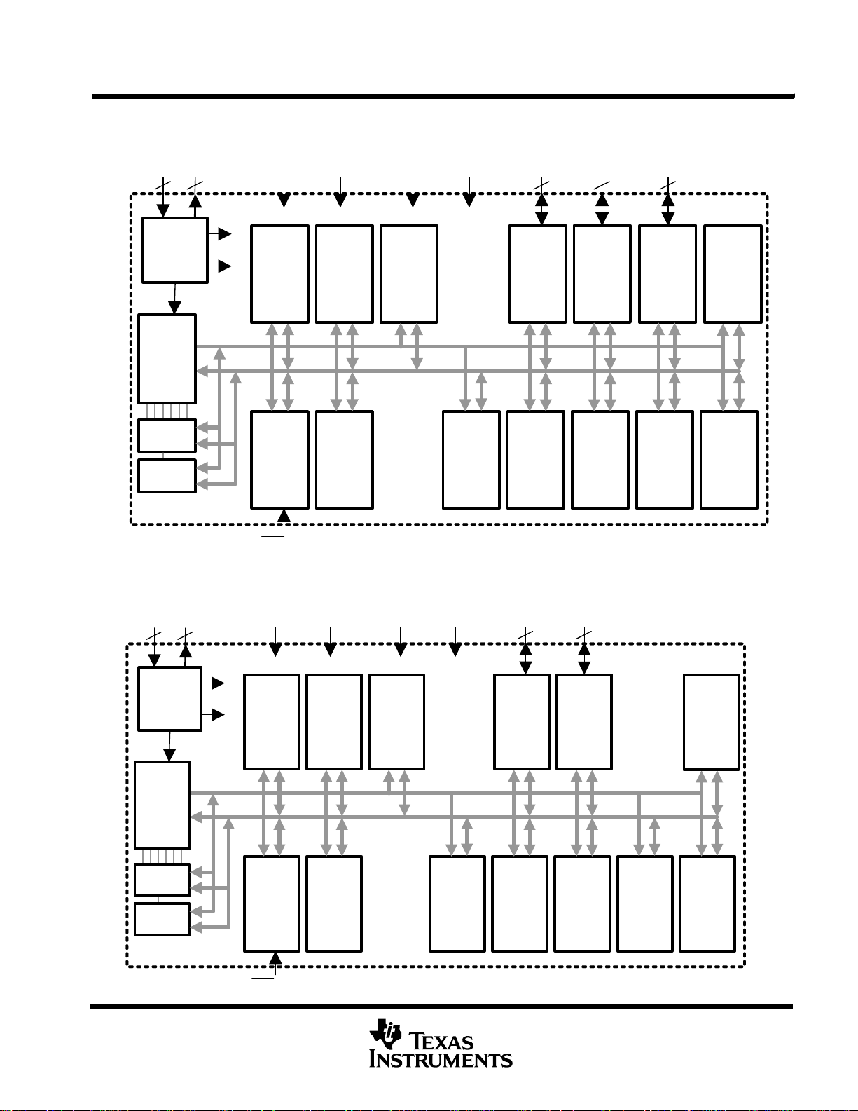
functional block diagram, MSP430F241x, 80-pin package
http://www.xinpian.net
提供单片机解密、IC解密、芯片解密业务
010-62245566 13810019655
MSP430x241x, MSP430x261x
MIXED SIGNAL MICROCONTROLLER
SLAS541A -- JUNE 2007 -- REVISED OCTOBER 2007
XIN/
XT2IN
Oscillators
Basic Clock
System+
16MHz
CPU
1MB
incl. 16
Registers
Emulation
JTAG
Interface
XOUT/
XT2OUT
22
MCLK
ACLK
SMCLK
DVCC1/2 DVSS1/2
Flash
120kB
116kB
92kB
92kB
MAB
MDB
Brownout
Protection
SVS,
SVM
RST/NMI
RAM
4kB
8kB
8kB
4kB
Hardware
Multiplier
MPY,
MPYS,
MAC,
MACS
AVCC AVSS P1.x/P2.x
ADC12
12-Bit
8
Channels
Watchdog
WDT+
15-Bit
Ports
P1/P2
2x8 I/O
Interrupt
capability
Timer_A3
3 CC
Registers
2x8
P3.x/P4.x
P5.x/P6.x
4x8
Ports
P3/P4
P5/P6
4x8 I/O
Timer_B7
7 CC
Registers,
Shadow
Reg
P7.x/P8.x
Ports
P7/P8
2x8/1x16
I/O
Comp_A+
8
Channels
2x8/
1x16
USCI A0
UART/
LIN,
IrDA, SPI
USCI B0
SPI, I2C
USCI A1
UART/
LIN,
IrDA, SPI
USCI B1
SPI, I2C
functional block diagram, MSP430F241x, 64-pin package
XOUT/
XIN/
XT2IN
Oscillators
Basic Clock
System+
16MHz
CPU
1MB
incl. 16
Registers
Emulation
JTAG
Interface
XT2OUT
22
ACLK
SMCLK
MCLK
DVCC DVSS
Flash
120kB
116kB
92kB
92kB
MAB
MDB
Brownout
Protection
SVS,
SVM
RAM
4kB
8kB
8kB
4kB
Hardware
Multiplier
MPY,
MPYS,
MAC,
MACS
AVCC AVSS P1.x/P2.x
ADC12
12-Bit
8
Channels
Watchdog
WDT+
15-Bit
Ports
P1/P2
2x8 I/O
Interrupt
capability
Timer_A3
3 CC
Registers
2x8
P3.x/P4.x
P5.x/P6.x
4x8
Ports
P3/P4
P5/P6
4x8 I/O
Timer_B7
7 CC
Registers,
Shadow
Reg
Comp_A+
8
Channels
USCI A0
UART/
LIN,
IrDA, SPI
USCI B0
SPI, I2C
USCI A1
UART/
LIN,
IrDA, SPI
USCI B1
SPI, I2C
RST/NMI
POST OFFICE BOX 655303 • DALLAS, TEXAS 75265
7
Page 8
MSP430x241x, MSP430x261x
http://www.xinpian.net
提供单片机解密、IC解密、芯片解密业务
010-62245566 13810019655
MIXED SIGNAL MICROCONTROLLER
SLAS541A -- JUNE 2007 -- REVISED OCTOBER 2007
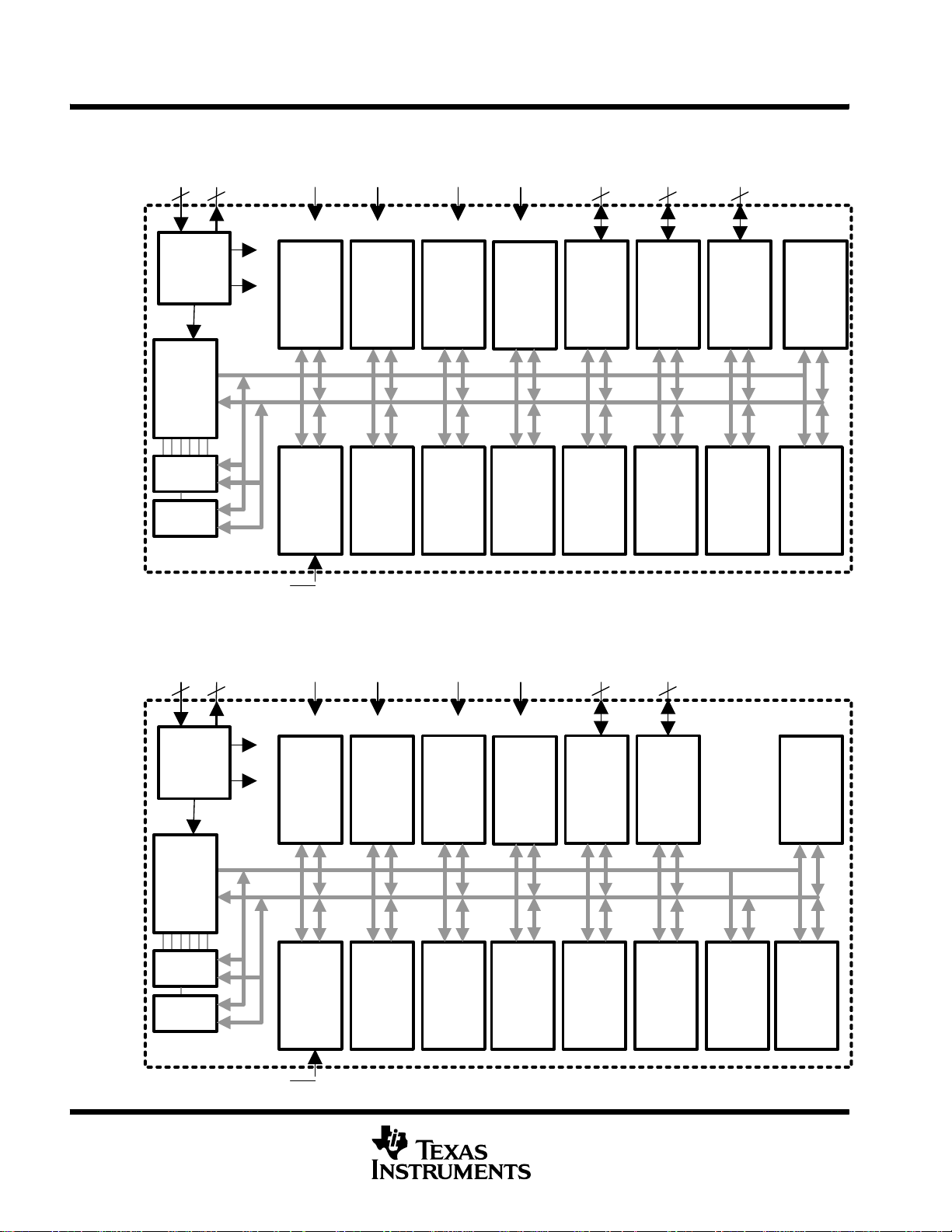
functional block diagram, MSP430F261x, 80-pin package
XIN/
XT2IN
Oscillators
Basic Clock
System+
16MHz
CPU
1MB
incl. 16
Registers
Emulation
JTAG
Interface
XOUT/
XT2OUT
22
MCLK
ACLK
SMCLK
DVCC1/2 DVSS1/2
Flash
120kB
116kB
92kB
92kB
56kB
MAB
MDB
Brownout
Protection
SVS,
SVM
RST/NMI
RAM
4kB
8kB
8kB
4kB
4kB
Hardware
Multiplier
MPY,
MPYS,
MAC,
MACS
AVCC AVSS P1.x/P2.x
ADC12
12-Bit
8
Channels
DMA
Controller
3
Channels
DAC12
12-Bit
2
Channels
Voltage
Out
Watchdog
WDT+
15-Bit
Ports
P1/P2
2x8 I/O
Interrupt
capability
Timer_A3
3 CC
Registers
2x8
P3.x/P4.x
P5.x/P6.x
4x8
Ports
P3/P4
P5/P6
4x8 I/O
Timer_B7
7 CC
Registers,
Shadow
Reg
P7.x/P8.x
Ports
P7/P8
2x8/1x16
I/O
Comp_A+
8
Channels
2x8/
1x16
USCI A0
UART/
LIN,
IrDA, SPI
USCI B0
SPI, I2C
USCI A1
UART/
LIN,
IrDA, SPI
USCI B1
SPI, I2C
functional block diagram, MSP430F261x, 64-pin package
XIN/
XT2IN
Oscillators
Basic Clock
System+
16MHz
CPU
1MB
incl. 16
Registers
Emulation
JTAG
Interface
XOUT/
XT2OUT
22
ACLK
SMCLK
MCLK
DVCC DVSS
Flash
120kB
116kB
92kB
92kB
56kB
MAB
MDB
Brownout
Protection
SVS,
SVM
RAM
4kB
8kB
8kB
4kB
4kB
Hardware
Multiplier
MPY,
MPYS,
MAC,
MACS
AVCC AVSS P1.x/P2.x
ADC12
12-Bit
8
Channels
DMA
Controller
3
Channels
DAC12
12-Bit
2
Channels
Voltage
Out
Watchdog
WDT+
15-Bit
Ports
P1/P2
2x8 I/O
Interrupt
capability
Timer_A3
3 CC
Registers
2x8
P3.x/P4.x
P5.x/P6.x
4x8
Ports
P3/P4
P5/P6
4x8 I/O
Timer_B7
7 CC
Registers,
Shadow
Reg
Comp_A+
8
Channels
USCI A0
UART/
LIN,
IrDA, SPI
USCI B0
SPI, I2C
USCI A1
UART/
LIN,
IrDA, SPI
USCI B1
SPI, I2C
8
RST/NMI
POST OFFICE BOX 655303 • DALLAS, TEXAS 75265
Page 9
MSP430x241x, MSP430x261x
I/ODESCRIPTIO
N
http://www.xinpian.net
提供单片机解密、IC解密、芯片解密业务
010-62245566 13810019655
MIXED SIGNAL MICROCONTROLLER
SLAS541A -- JUNE 2007 -- REVISED OCTOBER 2007
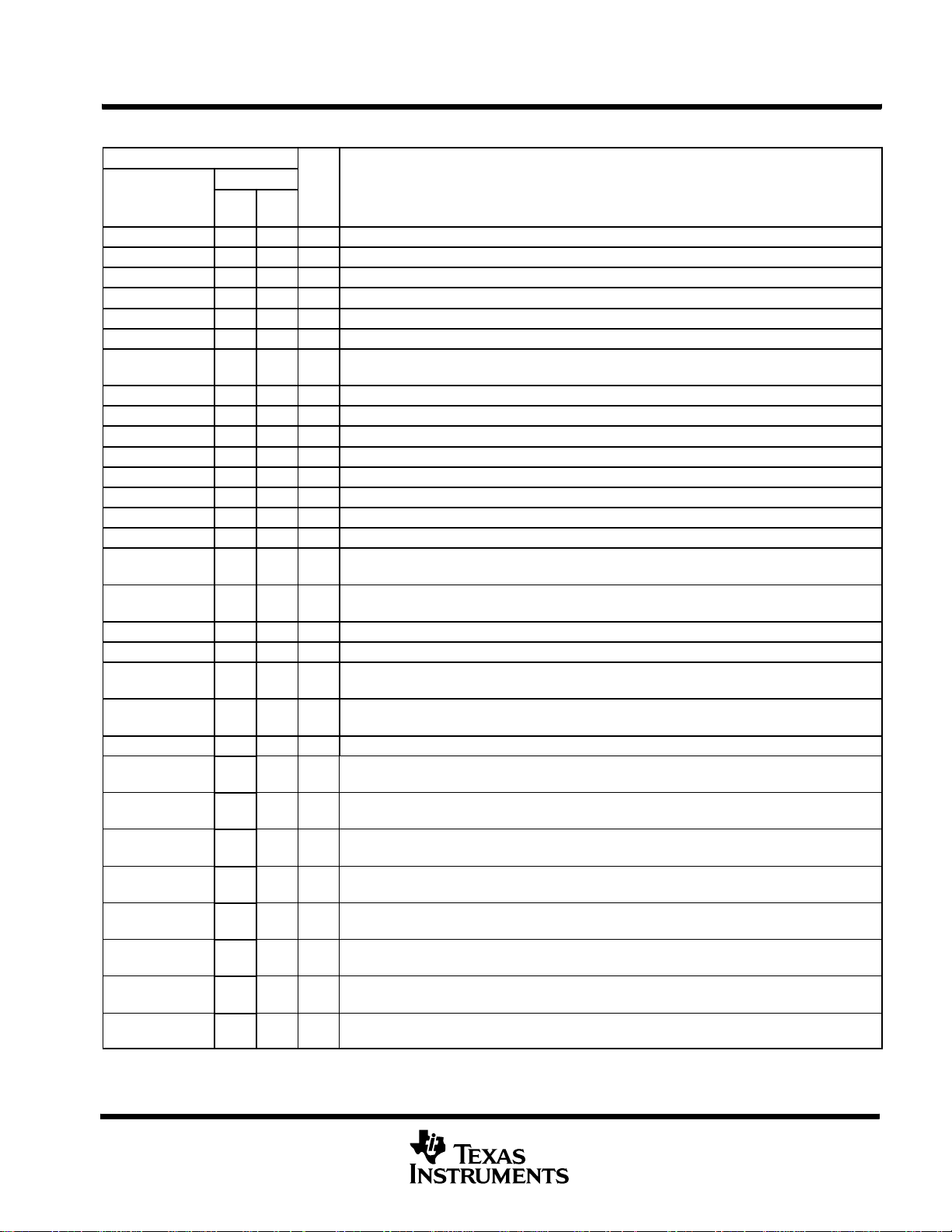
Terminal Functions
TERMINAL
NO.
NAME
AV
CC
AV
SS
DV
CC1
DV
SS1
DV
CC2
DV
SS2
P1.0/TACLK/
CAOUT
P1.1/TA0 13 13 I/O General-purpose digital I/O pin/Timer_A, capture: CCI0A input, compare: Out0 output/BSL transmit
P1.2/TA1 14 14 I/O General-purpose digital I/O pin/Timer_A, capture: CCI1A input, compare: Out1 output
P1.3/TA2 15 15 I/O General-purpose digital I/O pin/Timer_A, capture: CCI2A input, compare: Out2 output
P1.4/SMCLK 16 16 I/O General-purpose digital I/O pin/SMCLK signal output
P1.5/TA0 17 17 I/O General-purpose digital I/O pin/Timer_A, compare: Out0 output
P1.6/TA1 18 18 I/O General-purpose digital I/O pin/Timer_A, compare: Out1 output
P1.7/TA2 19 19 I/O General-purpose digital I/O pin/Timer_A, compare: Out2 output
P2.0/ACLK/CA2 20 20 I/O General-purpose digital I/O pin/ACLK output/Comparator_A input
P2.1/TAINCLK/
CA3
P2.2/CAOUT/
TA0 / C A 4
P2.3/CA0/TA1 23 23 I/O General-purpose digital I/O pin/Timer_A, compare: Out1 output/Comparator_A input
P2.4/CA1/TA2 24 24 I/O General-purpose digital I/O pin/Timer_A, compare: Out2 output/Comparator_A input
P2.5/Rosc/CA5 25 25 I/O
P2.6/ADC12CLK/
DMAE0†/CA6
P2.7/TA0/CA7 27 27 I/O General-purpose digital I/O pin/Timer_A, compare: Out0 output/Comparator_A input
P3.0/UCB0STE/
UCA0CLK
P3.1/UCB0SIMO/
UCB0SDA
P3.2/UCB0SOMI/
UCB0SCL
P3.3/UCB0CLK/
UCA0STE
P3.4/UCA0TXD/
UCA0SIMO
P3.5/UCA0RXD/
UCA0SOMI
P3.6/UCA1TXD/
UCA1SIMO
P3.7/UCA1RXD/
UCA1SOMI
†
MSP430F261x devices only
64
PIN80PIN
64 80 Analog supply voltage, positive terminal. Supplies only the analog portion of ADC12 and DAC12.
62 78 Analog supply voltage, negative terminal. Supplies only the analog portion of ADC12 and DAC12.
1 1 Digital supply voltage, positive terminal. Supplies all digital parts.
63 79 Digital supply voltage, negative terminal. Supplies all digital parts.
52 Digital supply voltage, positive terminal. Supplies all digital parts.
53 Digital supply voltage, negative terminal. Supplies all digital parts.
12 12 I/O General-purpose digital I/O pin/Timer_A, clock signal TACLK input/Comparator_A output
21 21 I/O General-purpose digital I/O pin/Timer_A, clock signal at INCLK
22 22 I/O
26 26 I/O
28 28 I/O General-purpose digital I/O pin/USCI B0 slave transmit enable/USCI A0 clock input/output
29 29 I/O General-purpose digital I/O pin/USCI B0 slave in/master out in SPI mode, SDA I2C data in I2Cmode
30 30 I/O General-purpose digital I/O pin/USCI B0 slave out/master in in SPI mode, SCL I2C clock in I2Cmode
31 31 I/O General-purpose digital I/O/USCI B0 clock input/output, USCI A0 slave transmit enable
32 32 I/O
33 33 I/O
34 34 I/O
35 35 I/O
General-purpose digital I/O pin/Timer_A, capture: CCI0B input/Comparator_A output/BSL
receive/Comparator_A input
General-purpose digital I/O pin/input for external resistor defining the DCO nominal
frequency/Comparator_A input
General-purpose digital I/O pin/conversion clock – 12 -bit ADC/DMA channel 0 external
trigger/Comparator_A input
General-purpose digital I/O pin/USCIA transmit data output in UART mode, slave data in/master out
in SPI mode
General-purpose digital I/O pin/USCI A0 receive data input in UART mode, slave data out/master
in in SPI mode
General-purpose digital I/O pin/USCI A1 transmit data output in UART mode, slave data in/master
out in SPI mode
General-purpose digital I/O pin/USCIA1 receive data input in UART mode, slave data out/master
in in SPI mode
POST OFFICE BOX 655303 • DALLAS, TEXAS 75265
9
Page 10
MSP430x241x, MSP430x261x
I/ODESCRIPTIO
N
http://www.xinpian.net
提供单片机解密、IC解密、芯片解密业务
010-62245566 13810019655
MIXED SIGNAL MICROCONTROLLER
SLAS541A -- JUNE 2007 -- REVISED OCTOBER 2007
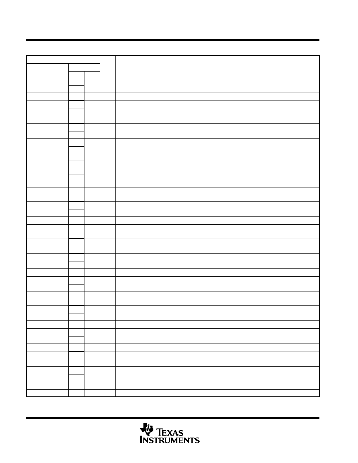
Terminal Functions (Continued)
TERMINAL
NO.
NAME
P4.0/TB0 36 36 I/O General-purpose digital I/O pin/Timer_B, capture: CCI0A/B input, compare: Out0 output
P4.1/TB1 37 37 I/O General-purpose digital I/O pin/Timer_B, capture: CCI1A/B input, compare: Out1 output
P4.2/TB2 38 38 I/O General-purpose digital I/O pin/Timer_B, capture: CCI2A/B input, compare: Out2 output
P4.3/TB3 39 39 I/O General-purpose digital I/O pin/Timer_B, capture: CCI3A/B input, compare: Out3 output
P4.4/TB4 40 40 I/O General-purpose digital I/O pin/Timer_B, capture: CCI4A/B input, compare: Out4 output
P4.5/TB5 41 41 I/O General-purpose digital I/O pin/Timer_B, capture: CCI5A/B input, compare: Out5 output
P4.6/TB6 42 42 I/O General-purpose digital I/O pin/Timer_B, capture: CCI6A input, compare: Out6 output
P4.7/TBCLK 43 43 I/O General-purpose digital I/O pin/Timer_B, clock signal TBCLK input
P5.0/UCB1STE/
UCA1CLK
P5.1/UCB1SIMO/
UCB1SDA
P5.2/UCB1SOMI/
UCB1SCL
P5.3/UCB1CLK/
UCA1STE
P5.4/MCLK 48 48 I/O General-purpose digital I/O pin/main system clock MCLK output
P5.5/SMCLK 49 49 I/O General-purpose digital I/O pin/submain system clock SMCLK output
P5.6/ACLK 50 50 I/O General-purpose digital I/O pin/auxiliary clock ACLK output
P5.7/TBOUTH/
SVSOUT
P6.0/A0 59 75 I/O General-purpose digital I/O pin/analog input A0 – 12-bit ADC
P6.1/A1 60 76 I/O General-purpose digital I/O pin/analog input A1 – 12-bit ADC
P6.2/A2 61 77 I/O General-purpose digital I/O pin/analog input A2 – 12-bit ADC
P6.3/A3 2 2 I/O General-purpose digital I/O pin/analog input A3 – 12-bit ADC
P6.4/A4 3 3 I/O General-purpose digital I/O pin/analog input A4 – 12-bit ADC
P6.5/A5/DAC1
P6.6/A6/DAC0
P6.7/A7/DAC1†/
SVSIN
P7.0 54 I/O General-purpose digital I/O pin
P7.1 55 I/O General-purpose digital I/O pin
P7.2 56 I/O General-purpose digital I/O pin
P7.3 57 I/O General-purpose digital I/O pin
P7.4 58 I/O General-purpose digital I/O pin
P7.5 59 I/O General-purpose digital I/O pin
P7.6 60 I/O General-purpose digital I/O pin
P7.7 61 I/O General-purpose digital I/O pin
P8.0 62 I/O General-purpose digital I/O pin
P8.1 63 I/O General-purpose digital I/O pin
P8.2 64 I/O General-purpose digital I/O pin
P8.3 65 I/O General-purpose digital I/O pin
†
MSP430F261x devices only
64
PIN80PIN
44 44 I/O General-purpose digital I/O pin/USCI B1 slave transmit enable/USCI A1 clock input/output
45 45 I/O General-purpose digital I/O pin/USCI B1slave in/master out in SPI mode, SDA I2C data in I2C mode
46 46 I/O General-purpose digital I/O pin/USCI B1slave out/master in in SPI mode, SCL I2C clock in I2C mode
47 47 I/O General-purpose digital I/O/USCI B1 clock input/output, USCI A1 slave transmit enable
51 51 I/O
†
4 4 I/O General-purpose digital I/O pin/analog input A5 – 12-bit ADC/DAC12.1 output
†
5 5 I/O General-purpose digital I/O pin/analog input A6 – 12-bit ADC/DAC12.0 output
6 6 I/O General-purpose digital I/O pin/analog input a7 – 12-bit ADC/DAC12.1 output/SVS input
General-purpose digital I/O pin/switch all PWM digital output ports to high impedance -- Timer_B
TB0 to TB6/SVS comparator output
10
POST OFFICE BOX 655303 • DALLAS, TEXAS 75265
Page 11
MSP430x241x, MSP430x261x
I/ODESCRIPTIO
N
http://www.xinpian.net
提供单片机解密、IC解密、芯片解密业务
010-62245566 13810019655
MIXED SIGNAL MICROCONTROLLER
SLAS541A -- JUNE 2007 -- REVISED OCTOBER 2007
Terminal Functions (Continued)
TERMINAL
NO.
NAME
P8.4 66 I/O General-purpose digital I/O pin
P8.5 67 I/O General-purpose digital I/O pin
P8.6/XT2OUT 68 O General-purpose digital I/O pin/Output terminal of crystal oscillator XT2
P8.7/XT2IN 69 I
XT2OUT 52 O Output terminal of crystal oscillator XT2
XT2IN 53 I Input port for crystal oscillator XT2
RST/NMI 58 74 I Reset input, nonmaskable interrupt input port, or bootstrap loader start (in flash devices).
TCK 57 73 I Test clock (JTAG). TCK is the clock input port for device programming test and bootstrap loader start.
TDI/TCLK 55 71 I Test data input or test clock input. The device protection fuse is connected to TDI/TCLK.
TDO/TDI 54 70 I/O Test data output port. TDO/TDI data output or programming data input terminal.
TMS 56 72 I Test mode select. TMS is used as an input port for device programming and test.
Ve
/DAC0
REF+
V
REF+
V
/Ve
REF--
REF--
XIN 8 8 I Input port for crystal oscillator XT1. Standard or watch crystals can be connected.
XOUT 9 9 O Output port for crystal oscillator XT1. Standard or watch crystals can be connected.
†
MSP430F261x devices only
64
PIN80PIN
General-purpose digital I/O pin/Input port for crystal oscillator XT2. Only standard crystals can be
connected.
†
10 10 I Input for an external reference voltage/DAC12.0 output
7 7 O Output of positive terminal of the reference voltage in the ADC12
11 11 I
Negative terminal for the reference voltage for both sources, the internal reference voltage, or an
external applied reference voltage
POST OFFICE BOX 655303 • DALLAS, TEXAS 75265
11
Page 12
MSP430x241x, MSP430x261x
http://www.xinpian.net
提供单片机解密、IC解密、芯片解密业务
010-62245566 13810019655
MIXED SIGNAL MICROCONTROLLER
SLAS541A -- JUNE 2007 -- REVISED OCTOBER 2007
short-form description
CPU
The MSP430 CPU has a 16-bit RISC architecture
that is highly transparent to the application. All
operations, other than program-flow instructions,
are performed as register operations in
conjunction with seven addressing modes for
source operand and four addressing modes for
destination operand.
The CPU is integrated with 16 registers that
provide reduced instruction execution time. The
register-to-register operation execution time is
one cycle of the CPU clock.
Four of the registers, R0 to R3, are dedicated as
program counter, stack pointer, status register,
and constant generator, respectively. The
remaining registers are general-purpose
registers.
Peripherals are connected to the CPU using data,
address, and control buses, and can be handled
with all instructions.
instruction set
The instruction set consists of 51 instructions with
three formats and seven address modes. Each
instruction can operate on word and byte data.
Table 1 shows examples of the three types of
instruction formats; the address modes are listed
in Table 2.
Program Counter
Stack Pointer
Status Register
Constant Generator
General-Purpose Register
General-Purpose Register
General-Purpose Register
General-Purpose Register
General-Purpose Register
General-Purpose Register
General-Purpose Register
General-Purpose Register
General-Purpose Register
General-Purpose Register
General-Purpose Register
General-Purpose Register
PC/R0
SP/R1
SR/CG1/R2
CG2/R3
R4
R5
R6
R7
R8
R9
R10
R11
R12
R13
R14
R15
Table 1. Instruction Word Formats
Dual operands, source-destination e.g., ADD R4,R5 R4 + R5 ------> R5
Single operands, destination only e.g., CALL R8 PC ---->(TOS), R8----> PC
Relative jump, un/conditional e.g., JNE Jump-on-equal bit = 0
Table 2. Address Mode Descriptions
ADDRESS MODE S D SYNTAX EXAMPLE OPERATION
Register D
Indexed D D MOV X(Rn),Y(Rm) MOV 2(R5),6(R6) M(2+R5)-- --> M(6+R6)
Symbolic (PC relative) D D MOV EDE,TONI M(EDE) ----> M(TONI)
Absolute D D MOV &MEM,&TCDAT M(MEM) -- --> M(TCDAT)
Indirect D MOV @Rn,Y(Rm) MOV @R10,Tab(R6) M(R10) -- --> M(Tab+R6)
Indirect
autoincrement
Immediate D MOV #X,TONI MOV #45,TONI #45 -- --> M(TONI)
NOTE: S = source D = destination
D
D MOV @Rn+,Rm MOV @R10+,R11
MOV Rs,Rd MOV R10,R11 R10 ----> R11
M(R10) -- --> R11
R10 + 2----> R10
12
POST OFFICE BOX 655303 • DALLAS, TEXAS 75265
Page 13

MSP430x241x, MSP430x261x
http://www.xinpian.net
提供单片机解密、IC解密、芯片解密业务
010-62245566 13810019655
MIXED SIGNAL MICROCONTROLLER
SLAS541A -- JUNE 2007 -- REVISED OCTOBER 2007
operating modes
The MSP430 has one active mode and five software selectable low-power modes of operation. An interrupt
event can wake up the device from any of the five low-power modes, service the request, and restore back to
the low-power mode on return from the interrupt program.
The following six operating modes can be configured by software:
D Active mode (AM)
-- All clocks are active.
D Low-power mode 0 (LPM0)
-- CPU is disabled.
ACLK and SMCLK remain active. MCLK is disabled.
D Low-power mode 1 (LPM1)
-- CPU is disabled.
ACLK and SMCLK remain active. MCLK is disabled.
DCO’s dc-generator is disabled if DCO not used in active mode.
D Low-power mode 2 (LPM2)
-- CPU is disabled.
MCLK and SMCLK are disabled.
DCO’s dc-generator remains enabled.
ACLK remains active.
D Low-power mode 3 (LPM3)
-- CPU is disabled.
MCLK and SMCLK are disabled.
DCO’s dc-generator is disabled.
ACLK remains active.
D Low-power mode 4 (LPM4)
-- CPU is disabled.
ACLK is disabled.
MCLK and SMCLK are disabled.
DCO’s dc-generator is disabled.
Crystal oscillator is stopped.
POST OFFICE BOX 655303 • DALLAS, TEXAS 75265
13
Page 14
MSP430x241x, MSP430x261x
0x0FFDAto1
3to0
Reserved(seeNotes7and8)Reserved
http://www.xinpian.net
提供单片机解密、IC解密、芯片解密业务
010-62245566 13810019655
MIXED SIGNAL MICROCONTROLLER
SLAS541A -- JUNE 2007 -- REVISED OCTOBER 2007
interrupt vector addresses
The interrupt vectors and the power-up starting address are located in the address range 0x0FFFF to 0x0FFC0.
The vector contains the 16-bit address of the appropriate interrupt-handler instruction sequence. If the reset
vector (0x0FFFE) contains 0xFFFF (e.g., flash is not programmed), the CPU enters LPM4 after power-up.
INTERRUPT SOURCE INTERRUPT FLAG SYSTEM INTERRUPT WORD ADDRESS PRIORITY
Power-up
External Reset
Watchdog
Flash Key Violation
PC out of range (see Note 1)
NMI
Oscillator Fault
Flash memory access violation
Timer_B7
Timer_B7
Comparator_A+ CAIFG Maskable 0x0FFF6 27
Watchdog timer+ WDTIFG Maskable 0x0FFF4 26
Timer_A3 TACCR0 CCIFG (see Note 3) Maskable 0x0FFF2 25
Timer_A3
USCI_A0/USCI_B0 receive
USCI_B0 I2C status
USCI_A0/USCI_B0 transmit
USCI_B0 I2C receive/transmit
ADC12 ADC12IFG (see Notes 2 and 3) Maskable 0x0FFEA 21
I/O port P2 (eight flags) P2IFG.0 to P2IFG.7 (see Notes 2 and 3) Maskable 0x0FFE6 19
I/O port P1 (eight flags) P1IFG.0 to P1IFG.7 (see Notes 2 and 3) Maskable 0x0FFE4 18
USCI_A0/USCI_B1 receive
USCI_B1 I2C status
USCI_A1/USCI_B1 transmit
USCI_B1 I2C receive/transmit
DMA
DAC12
NOTES: 1. A reset is executed if the CPU tries to fetch instructions from within the module register memory address range (0x00000 to 0x001FF)
or from within unused address ranges.
2. Multiple source flags.
3. Interrupt flags are located in the module.
4. In SPI mode: UCB0RXIFG. In I2C mode: UCALIFG, UCNACKIFG, ICSTTIFG, UCSTPIFG.
5. In UART/SPI mode: UCB0TXIFG. In I2C mode: UCB0RXIFG, UCB0TXIFG.
6. (Non)maskable: The individual interrupt-enable bit can disable an interrupt event, but the general-interrupt enable cannot.
7. The address 0x0FFBE is used as bootstrap loader security key (BSLSKEY).
A 0x0AA55 at this location disables the BSL completely.
A zero disables the erasure of the flash if an invalid password is supplied.
8. The interrupt vectors at addresses 0x0FFDA to 0x0FFC0 are not used in this device and can be used for regular program code if
necessary.
ACCVIFG (see Notes 2 and 6)
TBCCR1 to TBCCR6 CCIFGs, TBIFG
TAIFG (see Notes 2 and 3)
UCA0RXIFG, UCB0RXIFG
UCA0TXIFG, UCB0TXIFG
UCA1RXIFG, UCB1RXIFG
UCA1TXIFG, UCB1TXIFG
DMA0IFG, DMA1IFG, DMA2IFG
DAC12_0IFG, DAC12_1IFG
PORIFG
WDTIFG
RSTIFG
KEYV (see Note 2)
NMIIFG
OFIFG
TBCCR0 CCIFG
(see Note 3)
(see Notes 2 and 3)
TACCR1 CCIFG
TACCR2 CCIFG
(see Notes 2 and 4)
(see Note 2 and 4)
(see Notes 2 and 4)
(see Notes 2 and 5)
(see Notes 2 and 3)
(see Notes 2 and 3)
Reset 0x0FFFE 31, highest
(Non)maskable
(Non)maskable
(Non)maskable
Maskable 0x0FFFA 29
Maskable 0x0FFF8 28
Maskable 0x0FFF0 24
Maskable 0x0FFEE 23
Maskable 0x0FFEC 22
Maskable 0x0FFE2 17
Maskable 0x0FFE0 16
Maskable 0x0FFDE 15
Maskable 0x0FFDC 14
0x0FFFC 30
0x0FFE8 20
0x0FFC0 lowest
,
14
POST OFFICE BOX 655303 • DALLAS, TEXAS 75265
Page 15
MSP430x241x, MSP430x261x
http://www.xinpian.net
提供单片机解密、IC解密、芯片解密业务
010-62245566 13810019655
MIXED SIGNAL MICROCONTROLLER
SLAS541A -- JUNE 2007 -- REVISED OCTOBER 2007
special function registers
Most interrupt enable bits are collected in the lowest address space. Special-function register bits not allocated
to a functional purpose are not physically present in the device. This arrangement provides simple software
access.
interrupt enable 1 and 2
Address76543210
00h
WDTIE Watchdog timer interrupt enable. Inactive if watchdog mode is selected.
Active if watchdog timer is configured as general-purpose timer.
OFIE Oscillator-fault-interrupt enable
NMIIE Nonmaskable-interrupt enable
ACCVIE Flash memory access violation interrupt enable
ACCVIE NMIIE OFIE WDTIE
rw--0 rw--0 rw--0 rw--0
Interrupt Enable Register 1
Address76543210
01h
UCB0TXIE UCB0RXIE UCA0TXIE UCA0RXIE
rw--0 rw--0 rw--0 rw--0
Interrupt Enable Register 2
UCA0RXIE USCI_A0 receive-interrupt enable
UCA0TXIE USCI_A0 transmit-interrupt enable
UCB0RXIE USCI_B0 receive-interrupt enable
UCB0TXIE USCI_B0 transmit-interrupt enable
POST OFFICE BOX 655303 • DALLAS, TEXAS 75265
15
Page 16
MSP430x241x, MSP430x261x
http://www.xinpian.net
提供单片机解密、IC解密、芯片解密业务
010-62245566 13810019655
MIXED SIGNAL MICROCONTROLLER
SLAS541A -- JUNE 2007 -- REVISED OCTOBER 2007
interrupt flag register 1 and 2
Address76543210
02h
Interrupt Flag Register 1
WDTIFG Set on watchdog timer overflow or security key violation
Reset on V
power-on or a reset condition at the RST/NMI pin in reset mode
CC
OFIFG Flag set on oscillator fault7
PORIFG Power--on interrupt flag. Set on V
RSTIFG External reset interrupt flag. Set on a reset condition at RST
on V
NMIIFG Set via RST
Address76543210
03h
power up.
CC
/NMI pin
NMIIFG RSTIFG PORIFG OFIFG WDTIFG
rw--0 rw--(0) rw--(1) rw--1 rw --(0)
power up.
CC
UCB0TX
IFG
rw--1 rw--0 rw--1 rw--0
/NMI pin in reset mode. Reset
UCB0RX
IFG
UCA0TX
IFG
UCA0RX
IFG
Interrupt Flag Register 2
UCA0RXIFG USCI_A0 receive-interrupt flag
UCA0TXIFG USCI_A0 transmit-interrupt flag
UCB0RXIFG USCI_B0 receive-interrupt flag
UCB0TXIFG USCI_B0 transmit-interrupt flag
Legend rw: Bit can be read and written.
rw-0,1: B it can be read and w ritten. It is R eset or Set by PU C.
rw-(0,1) B it can be read and w ritten. It is R eset or Set by PO R.
SFR bit is not present in device.
16
POST OFFICE BOX 655303 • DALLAS, TEXAS 75265
Page 17
memory organization
http://www.xinpian.net
提供单片机解密、IC解密、芯片解密业务
010-62245566 13810019655
MSP430x241x, MSP430x261x
MIXED SIGNAL MICROCONTROLLER
SLAS541A -- JUNE 2007 -- REVISED OCTOBER 2007
Memory
Main: interrupt vector
Main: code memory
RAM (total)
Extended
Mirrored
Information memory Size
Boot memory Size
RAM (mirrored at
0x18FF to 0x01100)
Peripherals 16-bit
Memory
Main: interrupt vector
Main: code memory
RAM (total)
Extended
Mirrored
Information memory Size
Boot memory Size
RAM (mirrored at
0x18FF to 0x01100)
Peripherals 16-bit
Size
Flash
Flash
Size
Size
Size
Flash
ROM
Size 2KB
8-bit
8-bit SFR
Size
Flash
Flash
Size
Size
Size
Flash
ROM
Size 2KB
8-bit
8-bit SFR
MSP430F2416
MSP430F2616
92KB
0x0FFFF -- 0x0FFC0
0x18FFF -- 0x02100
4kB
0x020FF -- 0x01100
2kB
0x020FF -- 0x01900
2kB
0x018FF -- 0x01100
256 Byte
0x010FF -- 0x01000
1KB
0x00FFF -- 0x00C00
0x009FF -- 0x00200
0x001FF -- 0x00100
0x000FF -- 0x00010
0x0000F -- 0x00000
MSP430F2618
MSP430F2418
116KB
0x0FFFF -- 0x0FFC0
0x1FFFF -- 0x03100
8kB
0x030FF -- 0x01100
6kB
0x030FF -- 0x01900
2kB
0x018FF -- 0x01100
256 Byte
0x010FF -- 0x01000
1KB
0x00FFF -- 0x00C00
0x009FF -- 0x00200
0x001FF -- 0x00100
0x000FF -- 0x00010
0x0000F -- 0x00000
MSP430F2417
MSP430F2617
92KB
0x0FFFF -- 0x0FFC0
0x19FFF -- 0x03100
8kB
0x030FF -- 0x01100
6kB
0x030FF -- 0x01900
2kB
0x018FF -- 0x01100
256 Byte
0x010FF -- 0x01000
1KB
0x00FFF -- 0x00C00
2KB
0x009FF -- 0x00200
0x001FF -- 0x00100
0x000FF -- 0x00010
0x0000F -- 0x00000
MSP430F2619
MSP430F2419
120KB
0x0FFFF -- 0x0FFC0
0x1FFFF -- 0x02100
4kB
0x020FF -- 0x01100
2kB
0x020FF -- 0x01900
2kB
0x018FF -- 0x01100
256 Byte
0x010FF -- 0x01000
1KB
0x00FFF -- 0x00C00
2KB
0x009FF -- 0x00200
0x001FF -- 0x00100
0x000FF -- 0x00010
0x0000F -- 0x00000
bootstrap loader (BSL)
The MSP430 BSL enables users to program the flash memory or RAM using a UART serial interface. Access
to the MSP430 memory via the BSL is protected by a user-defined password. For complete description of the
features of the BSL and its implementation, see the application report Features of the MSP430 Bootstrap
Loader, literature number SLAA089.
BSL Function PM, RTD Package Pins
Data Transmit 13 - P1.1
Data Receive 22 - P2.2
POST OFFICE BOX 655303 • DALLAS, TEXAS 75265
17
Page 18

MSP430x241x, MSP430x261x
http://www.xinpian.net
提供单片机解密、IC解密、芯片解密业务
010-62245566 13810019655
MIXED SIGNAL MICROCONTROLLER
SLAS541A -- JUNE 2007 -- REVISED OCTOBER 2007
flash memory
The flash memory can be programmed via the JTAG port, the bootstrap loader, or in-system by the CPU. The
CPU can perform single-byte and single-word writes to the flash memory. Features of the flash memory include:
D Flash memory has n segments of main memory and four segments of information memory (A to D) of 64
bytes each. Each segment in main memory is 512 bytes in size.
D Segments 0 to n may be erased in one step, or each segment may be individually erased.
D Segments A to D can be erased individually, or as a group with segments 0 to n.
Segments A to D are also called information memory.
D Segment A contains calibration data. After reset, segment A is protected against programming or erasing.
It can be unlocked, but care should be taken not to erase this segment if the calibration data is required.
D Flash content integrity check with marginal read modes
peripherals
Peripherals are connected to the CPU through data, address, and control buses and can be handled using all
instructions. For complete module descriptions, see the MSP430x2xx Family User’s Guide, literature number
SLAU144.
DMA controller
The DMA controller allows movement of data from one memory address to another without CPU intervention.
For example, the DMA controller can be used to move data from the ADC12 conversion memory to RAM. Using
the DMA controller can increase the throughput of peripheral modules. The DMA controller reduces system
power consumption by allowing the CPU to remain in sleep mode without having to awaken to move data to
or from a peripheral.
oscillator and system clock
The clock system in the MSP430x241x and MSP43x261x family of devices is supported by the basic clock
module that includes support for a 32768-Hz watch crystal oscillator, an internal very low power, low frequency
oscillator,an internal digitally-controlled oscillator (DCO) and a high frequency crystal oscillator. The basic clock
module is designed to meet the requirements of both low system cost and low-power consumption. The internal
DCO provides a fast turn-on clock source and stabilizes in less than 1 μs. The basic clock module provides the
following clock signals:
D Auxiliary clock (ACLK), sourced from a 32768-Hz watch crystal, a high frequency crystal, or a very
low-power LF oscillator
D Main clock (MCLK), the system clock used by the CPU
D Sub-Main clock (SMCLK), the subsystem clock used by the peripheral modules
The DCO settings to calibrate the DCO output frequency are stored in the information memory segment A.
18
POST OFFICE BOX 655303 • DALLAS, TEXAS 75265
Page 19
MSP430x241x, MSP430x261x
http://www.xinpian.net
提供单片机解密、IC解密、芯片解密业务
010-62245566 13810019655
MIXED SIGNAL MICROCONTROLLER
SLAS541A -- JUNE 2007 -- REVISED OCTOBER 2007
calibration data stored in information memory segment A
Calibration data is stored for the DCO and for the ADC12. It is organized in a tag-length-value (TLV) structure.
TAGS USED BY THE ADC CALIBRATION TAGS
NAME ADDRESS VALU E DESCRIPTION
TAG_DCO_30 0x10F6 0x01 DCO frequency calibration at VCC = 3 V and TA=25°C at calibration
TAG_ADC12_1 0x10DA 0x10 ADC12_1 calibration tag
TAG_EMPTY -- 0xFE Identifier for empty memory areas
LABELS USED BY THE ADC CALIBRATION TAGS
LABEL CONDITION AT CALIBRATION / DESCRIPTION SIZE ADDRESS OFFSET
CAL_ADC_25T85 INCHx = 0x1010; REF2_5 = 1, TA=85°C word 0x000E
CAL_ADC_25T30 INCHx = 0x1010; REF2_5 = 1, TA=30°C word 0x000C
CAL_ADC_25VREF_FACTOR REF2_5 = 1, TA=30°C word 0x000A
CAL_ADC_15T85 INCHx = 0x1010; REF2_5 = 0, TA=85°C word 0x0008
CAL_ADC_15T30 INCHx = 0x1010; REF2_5 = 0, TA=30°C word 0x0006
CAL_ADC_15VREF_FACTOR REF2_5 = 0, TA=30°C word 0x0004
CAL_ADC_OFFSET External V
CAL_ADC_GAIN_FACTOR External V
CAL_BC1_1MHz -- byte 0x0007
CAL_DCO_1MHz -- byte 0x0006
CAL_BC1_8MHz -- byte 0x0005
CAL_DCO_8MHz -- byte 0x0004
CAL_BC1_12MHz -- byte 0x0003
CAL_DCO_12MHz -- byte 0x0002
CAL_BC1_16MHz -- byte 0x0001
CAL_DCO_16MHz -- byte 0x0000
REF
REF
=1.5V,f
=1.5V,f
ADC12CLK
ADC12CLK
=5MHz word 0x0002
=5MHz word 0x0000
brownout, supply voltage supervisor (SVS)
The brownout circuit is implemented to provide the proper internal reset signal to the device during power on
and power off. The SVS circuitry detects if the supply voltage drops below a user selectable level and supports
both supply voltage supervision (the device is automatically reset) and supply voltage monitoring (SVM, the
device is not automatically reset).
The CPU begins code execution after the brownout circuit releases the device reset. However, V
have ramped to V
reaches V
V
CC
CC(min)
CC(min)
at that time. The user must ensure that the default DCO settings are not changed until
. If desired, the SVS circuit can be used to determine when VCCreaches V
may not
CC
CC(min)
.
POST OFFICE BOX 655303 • DALLAS, TEXAS 75265
19
Page 20

MSP430x241x, MSP430x261x
http://www.xinpian.net
提供单片机解密、IC解密、芯片解密业务
010-62245566 13810019655
MIXED SIGNAL MICROCONTROLLER
SLAS541A -- JUNE 2007 -- REVISED OCTOBER 2007
digital I/O
There are up to eight 8-bit I/O ports implemented—ports P1 through P8:
D All individual I/O bits are independently programmable.
D Any combination of input, output, and interrupt conditions is possible.
D Edge-selectable interrupt input capability for all eight bits of ports P1 and P2.
D Read/write access to port-control registers is supported by all instructions.
D Each I/O has an individually programmable pullup/pulldown r esistor.
D Ports P7/P8 can be accessed word wise.
watchdog timer+ (WDT+)
The primary function of the WDT+ module is to perform a controlled system restart after a software problem
occurs. If the selected time interval expires, a system reset is generated. If the watchdog function is not needed
in an application, the module can be configured as an interval timer and can generate interrupts at selected time
intervals.
hardware multiplier
The multiplication operation is supported by a dedicated peripheral module. The module performs 16×16,
16×8, 8×16, and 8×8 bit operations. The module is capable of supporting signed and unsigned multiplication
as well as signed and unsigned multiply and accumulate operations. The result of an operation can be accessed
immediately after the operands have been loaded into the peripheral registers. No additional clock cycles are
required.
universal serial communication interface (USCI)
The USCI modules are used for serial data communication. The USCI module supports synchronous
communication protocols such as SPI (3 pin or 4 pin) or I
UART, enhanced UART with automatic baudrate detection (LIN), and IrDA.
The USCI A module provides support for SPI (3 pin or 4 pin), UART, enhanced UART, and IrDA.
The USCI B module provides support for SPI (3 pin or 4 pin) and I
2
C, and asynchronous combination protocols such as
2
C.
20
POST OFFICE BOX 655303 • DALLAS, TEXAS 75265
Page 21
MSP430x241x, MSP430x261x
A
http://www.xinpian.net
提供单片机解密、IC解密、芯片解密业务
010-62245566 13810019655
MIXED SIGNAL MICROCONTROLLER
SLAS541A -- JUNE 2007 -- REVISED OCTOBER 2007
timer_A3
Timer_A3 is a 16-bit timer/counter with three capture/compare registers. Timer_A3 can support multiple
capture/compares, PWM outputs, and interval timing. Timer_A3 also has extensive interrupt capabilities.
Interrupts may be generated from the counter on overflow conditions and from each of the capture/compare
registers.
TIMER_A3 SIGNAL CONNECTIONS
INPUT PIN
NUMBER
12 - P1.0 TACLK TACL K
21 - P2.1 TAINCLK INCLK
13 - P1.1 TA 0 CCI0A
22 - P2.2 TA 0 CCI0B
14 - P1.2 TA 1 CCI1A
15 - P1.3 TA 2 CCI2A
DEVICE INPUT
SIGNAL
ACLK ACLK
SMCLK SMCLK
DV
SS
DV
CC
CAOUT (internal) CCI1B
DV
SS
DV
CC
ACLK (internal) CCI2B
DV
SS
DV
CC
MODULE INPUT
NAME
GND
V
CC
GND
V
CC
GND
V
CC
MODULE
BLOCK
Timer N
CCR0 TA0
CCR1
CCR2 TA2
MODULE OUTPUT
SIGNAL
TA1
OUTPUT PIN NUMBER
13 - P1.1
17 - P1.5
27 - P2.7
14 - P1.2
18 - P1.6
23 - P2.3
ADC12 (internal)
DAC12_0 (internal)
DAC12_1 (internal)
15 - P1.3
19 - P1.7
24 - P2.4
POST OFFICE BOX 655303 • DALLAS, TEXAS 75265
21
Page 22
MSP430x241x, MSP430x261x
A
http://www.xinpian.net
提供单片机解密、IC解密、芯片解密业务
010-62245566 13810019655
MIXED SIGNAL MICROCONTROLLER
SLAS541A -- JUNE 2007 -- REVISED OCTOBER 2007
timer_B7
Timer_B7 is a 16-bit timer/counter with seven capture/compare registers. Timer_B7 can support multiple
capture/compares, PWM outputs, and interval timing. Timer_B7 also has extensive interrupt capabilities.
Interrupts may be generated from the counter on overflow conditions and from each of the capture/compare
registers.
TIMER_B3/B7 SIGNAL CONNECTIONS
INPUT PIN
NUMBER
DEVICE INPUT
SIGNAL
MODULE INPUT
NAME
43 - P4.7 TBCLK TBCLK
ACLK ACLK
SMCLK SMCLK
43 - P4.7 TBCLK INCLK
36 - P4.0 TB0 CCI0A
36 - P4.0 TB0 CCI0B
DV
DV
SS
CC
GND
V
CC
37 - P4.1 TB1 CCI1A
37 - P4.1 TB1 CCI1B
DV
DV
SS
CC
GND
V
CC
38 - P4.2 TB2 CCI2A
38 - P4.2 TB2 CCI2B
DV
DV
SS
CC
GND
V
CC
39 - P4.3 TB3 CCI3A
39 - P4.3 TB3 CCI3B
DV
DV
SS
CC
GND
V
CC
40 - P4.4 TB4 CCI4A
40 - P4.4 TB4 CCI4B
DV
DV
SS
CC
GND
V
CC
41 - P4.5 TB5 CCI5A
41 - P4.5 TB5 CCI5B
DV
DV
SS
CC
GND
V
CC
42 - P4.6 TB6 CCI6A
ACLK (internal) CCI6B
DV
DV
SS
CC
GND
V
CC
†
MODULE
BLOCK
MODULE OUTPUT
SIGNAL
Timer N
CCR0 TB0
CCR1 TB1
CCR2 TB2
CCR3 TB3
CCR4 TB4
CCR5 TB5
CCR6 TB6
OUTPUT PIN NUMBER
36 - P4.0
ADC12 (internal)
37 - P4.1
ADC12 (internal)
38 - P4.2
DAC_0(internal)
DAC_1(internal)
39 - P4.3
40 - P4.4
41 - P4.5
42 - P4.6
22
POST OFFICE BOX 655303 • DALLAS, TEXAS 75265
Page 23

MSP430x241x, MSP430x261x
http://www.xinpian.net
提供单片机解密、IC解密、芯片解密业务
010-62245566 13810019655
MIXED SIGNAL MICROCONTROLLER
SLAS541A -- JUNE 2007 -- REVISED OCTOBER 2007
comparator_A+
The primary function of the comparator_A+ module is to support precision slope analog-to-digital conversions,
battery-voltage supervision, and monitoring of external analog signals.
ADC12
The ADC12 module supports fast, 12-bit analog-to-digital conversions. The module implements a 12-bit SAR
core, sample select control, reference generator, and a 16-word conversion-and-control buffer. The
conversion-and-control buffer allows up to 16 independent ADC samples to be converted and stored without
any CPU intervention.
DAC12
The DAC12 module is a 12-bit, R-ladder, voltage output DAC. The DAC12 may be used in 8-bit or 12-bit mode
and may be used in conjunction with the DMA controller. When multiple DAC12 modules are present, they may
be grouped together for synchronous operation.
POST OFFICE BOX 655303 • DALLAS, TEXAS 75265
23
Page 24
MSP430x241x, MSP430x261x
http://www.xinpian.net
提供单片机解密、IC解密、芯片解密业务
010-62245566 13810019655
MIXED SIGNAL MICROCONTROLLER
SLAS541A -- JUNE 2007 -- REVISED OCTOBER 2007
peripheral file map
†
DMA
†
DAC12
ADC12
†
MSP430F261x devices only
DMA channel 2 transfer size DMA2SZ 0x01F2
DMA channel 2 destination address DMA2DA 0x01EE
DMA channel 2 source address DMA2SA 0x01EA
DMA channel 2 control DMA2CTL 0x01E8
DMA channel 1 transfer size DMA1SZ 0x01E6
DMA channel 1 destination address DMA1DA 0x01E2
DMA channel 1 source address DMA1SA 0x01DE
DMA channel 1 control DMA1CTL 0x01DC
DMA channel 0 transfer size DMA0SZ 0x01DA
DMA channel 0 destination address DMA0DA 0x01D6
DMA channel 0 source address DMA0SA 0x01D2
DMA channel 0 control DMA0CTL 0x01D0
DMA module interrupt vector word DMAIV 0x0126
DMA module control 1 DMACTL1 0x0124
DMA module control 0 DMACTL0 0x0122
DAC12_1 data DAC12_1DAT 0x01CA
DAC12_1 control DAC12_1CTL 0x01C2
DAC12_0 data DAC12_0DAT 0x01C8
DAC12_0 control DAC12_0CTL 0x01C0
Interrupt-vector-word register ADC12IV 0x01A8
Inerrupt-enable register ADC12IE 0x01A6
Inerrupt-flag register ADC12IFG 0x01A4
Control register 1 ADC12CTL1 0x01A2
Control register 0 ADC12CTL0 0x01A0
Conversion memory 15 ADC12MEM15 0x015E
Conversion memory 14 ADC12MEM14 0x015C
Conversion memory 13 ADC12MEM13 0x015A
Conversion memory 12 ADC12MEM12 0x0158
Conversion memory 11 ADC12MEM11 0x0156
Conversion memory 10 ADC12MEM10 0x0154
Conversion memory 9 ADC12MEM9 0x0152
Conversion memory 8 ADC12MEM8 0x0150
Conversion memory 7 ADC12MEM7 0x014E
Conversion memory 6 ADC12MEM6 0x014C
Conversion memory 5 ADC12MEM5 0x014A
Conversion memory 4 ADC12MEM4 0x0148
Conversion memory 3 ADC12MEM3 0x0146
Conversion memory 2 ADC12MEM2 0x0144
Conversion memory 1 ADC12MEM1 0x0142
Conversion memory 0 ADC12MEM0 0x0140
PERIPHERAL FILE MAP
24
POST OFFICE BOX 655303 • DALLAS, TEXAS 75265
Page 25
ADC12
_
_
http://www.xinpian.net
提供单片机解密、IC解密、芯片解密业务
010-62245566 13810019655
(continued)
Timer_B7
Timer_A3
MSP430x241x, MSP430x261x
MIXED SIGNAL MICROCONTROLLER
SLAS541A -- JUNE 2007 -- REVISED OCTOBER 2007
PERIPHERAL FILE MAP (CONTINUED)
ADC memory-control register15 ADC12MCTL15 0x008F
ADC memory-control register14 ADC12MCTL14 0x008E
ADC memory-control register13 ADC12MCTL13 0x008D
ADC memory-control register12 ADC12MCTL12 0x008C
ADC memory-control register11 ADC12MCTL11 0x008B
ADC memory-control register10 ADC12MCTL10 0x008A
ADC memory-control register9 ADC12MCTL9 0x0089
ADC memory-control register8 ADC12MCTL8 0x0088
ADC memory-control register7 ADC12MCTL7 0x0087
ADC memory-control register6 ADC12MCTL6 0x0086
ADC memory-control register5 ADC12MCTL5 0x0085
ADC memory-control register4 ADC12MCTL4 0x0084
ADC memory-control register3 ADC12MCTL3 0x0083
ADC memory-control register2 ADC12MCTL2 0x0082
ADC memory-control register1 ADC12MCTL1 0x0081
ADC memory-control register0 ADC12MCTL0 0x0080
Capture/compare register 6 TBCCR6 0x019E
Capture/compare register 5 TBCCR5 0x019C
Capture/compare register 4 TBCCR4 0x019A
Capture/compare register 3 TBCCR3 0x0198
Capture/compare register 2 TBCCR2 0x0196
Capture/compare register 1 TBCCR1 0x0194
Capture/compare register 0 TBCCR0 0x0192
Timer_B register TBR 0x0190
Capture/compare control 6 TBCCTL6 0x018E
Capture/compare control 5 TBCCTL5 0x018C
Capture/compare control 4 TBCCTL4 0x018A
Capture/compare control 3 TBCCTL3 0x0188
Capture/compare control 2 TBCCTL2 0x0186
Capture/compare control 1 TBCCTL1 0x0184
Capture/compare control 0 TBCCTL0 0x0182
Timer_B control TBCTL 0x0180
Timer_B interrupt vector TBIV 0x011E
Capture/compare register 2 TACCR2 0x0176
Capture/compare register 1 TACCR1 0x0174
Capture/compare register 0 TACCR0 0x0172
Timer_A register TAR 0x0170
Reserved 0x016E
Reserved 0x016C
Reserved 0x016A
Reserved 0x0168
Capture/compare control 2 TACCTL2 0x0166
Capture/compare control 1 TACCTL1 0x0164
Capture/compare control 0 TACCTL0 0x0162
Timer_A control TAC T L 0x0160
Timer_A interrupt vector TAIV 0x012E
POST OFFICE BOX 655303 • DALLAS, TEXAS 75265
25
Page 26
MSP430x241x, MSP430x261x
/
/
http://www.xinpian.net
提供单片机解密、IC解密、芯片解密业务
010-62245566 13810019655
MIXED SIGNAL MICROCONTROLLER
SLAS541A -- JUNE 2007 -- REVISED OCTOBER 2007
PERIPHERAL FILE MAP (CONTINUED)
Hardware
Multiplier
Flash
Watchdog Watchdog Timer control WDTCTL 0x0120
USCI A0/B0
USCI A1/B1
Sum extend SUMEXT 0x013E
Result high word RESHI 0x013C
Result low word RESLO 0x013A
Second operand OP2 0x0138
Multiply signed +accumulate/operand1 MACS 0x0136
Multiply+accumulate/operand1 MAC 0x0134
Multiply signed/operand1 MPYS 0x0132
Multiply unsigned/operand1 MPY 0x0130
Flash control 4 FCTL4 0x01BE
Flash control 3 FCTL3 0x012C
Flash control 2 FCTL2 0x012A
Flash control 1 FCTL1 0x0128
USCI A0 auto baud rate control UCA0ABCTL 0x005D
USCI A0 transmit buffer UCA0TXBUF 0x0067
USCI A0 receive buffer UCA0RXBUF 0x0066
USCI A0 status UCA0STAT 0x0065
USCI A0 modulation control UCA0MCTL 0x0064
USCI A0 baud rate control 1 UCA0BR1 0x0063
USCI A0 baud rate control 0 UCA0BR0 0x0062
USCI A0 control 1 UCA0CTL1 0x0061
USCI A0 control 0 UCA0CTL0 0x0060
USCI A0 IrDA receive control UCA0IRRCTL 0x005F
USCI A0 IrDA transmit control UCA0IRTCLT 0x005E
USCI B0 transmit buffer UCB0TXBUF 0x006F
USCI B0 receive buffer UCB0RXBUF 0x006E
USCI B0 status UCB0STAT 0x006D
USCI B0 I2C Interrupt enable UCB0CIE 0x006C
USCI B0 baud rate control 1 UCB0BR1 0x006B
USCI B0 baud rate control 0 UCB0BR0 0x006A
USCI B0 control 1 UCB0CTL1 0x0069
USCI B0 control 0 UCB0CTL0 0x0068
USCI B0 I2C slave address UCB0SA 0x011A
USCI B0 I2C own address UCB0OA 0x0118
USCI A1 auto baud rate control UCA1ABCTL 0x00CD
USCI A1 transmit buffer UCA1TXBUF 0x00D7
USCI A1 receive buffer UCA1RXBUF 0x00D6
USCI A1 status UCA1STAT 0x00D5
USCI A1 modulation control UCA1MCTL 0x00D4
USCI A1 baud rate control 1 UCA1BR1 0x00D3
USCI A1 baud rate control 0 UCA1BR0 0x00D2
USCI A1 control 1 UCA1CTL1 0x00D1
USCI A1 control 0 UCA1CTL0 0x00D0
USCI A1 IrDA receive control UCA1IRRCTL 0x00CF
USCI A1 IrDA transmit control UCA1IRTCLT 0x00CE
26
POST OFFICE BOX 655303 • DALLAS, TEXAS 75265
Page 27
MSP430x241x, MSP430x261x
/
p
_
http://www.xinpian.net
提供单片机解密、IC解密、芯片解密业务
010-62245566 13810019655
MIXED SIGNAL MICROCONTROLLER
SLAS541A -- JUNE 2007 -- REVISED OCTOBER 2007
PERIPHERAL FILE MAP (CONTINUED)
USCI A1/B1
(continued)
Comparator_A+
Basic Clock
Brownout, SVS SVS control register (reset by brownout signal) SVSCTL 0x0055
†
Port PA
†
Port P8
†
Port P7
Port P6
Port P5
†
80-pin devices only
USCI B1 transmit buffer UCB1TXBUF 0x00DF
USCI B1 receive buffer UCB1RXBUF 0x00DE
USCI B1 status UCB1STAT 0x00DD
USCI B1 I2C Interrupt enable UCB1CIE 0x00DC
USCI B1 baud rate control 1 UCB1BR1 0x00DB
USCI B1 baud rate control 0 UCB1BR0 0x00DA
USCI B1 control 1 UCB1CTL1 0x00D9
USCI B1 control 0 UCB1CTL0 0x00D8
USCI B1 I2C slave address UCB1SA 0x017E
USCI B1 I2C own address UCB1OA 0x017C
USCI A1/B1 interrupt enable UC1IE 0x0006
USCI A1/B1 interrupt flag UC1IFG 0x0007
Comparator_A port disable CAPD 0x005B
Comparator_A control2 CACTL2 0x005A
Comparator_A control1 CACTL1 0x0059
Basic clock system control3 BCSCTL3 0x0053
Basic clock system control2 BCSCTL2 0x0058
Basic clock system control1 BCSCTL1 0x0057
DCO clock frequency control DCOCTL 0x0056
Port PA resistor enable PAREN 0x0014
Port PA selection PASEL 0x003E
Port PA direction PAD I R 0x003C
Port PA output PAO U T 0x003A
Port PA input PAI N 0x0038
Port P8 resistor enable P8REN 0x0015
Port P8 selection P8SEL 0x003F
Port P8 direction P8DIR 0x003D
Port P8 output P8OUT 0x003B
Port P8 input P8IN 0x0039
Port P7 resistor enable P7REN 0x0014
Port P7 selection P7SEL 0x003E
Port P7 direction P7DIR 0x003C
Port P7 output P7OUT 0x003A
Port P7 input P7IN 0x0038
Port P6 resistor enable P6REN 0x0013
Port P6 selection P6SEL 0x0037
Port P6 direction P6DIR 0x0036
Port P6 output P6OUT 0x0035
Port P6 input P6IN 0x0034
Port P5 resistor enable P5REN 0x0012
Port P5 selection P5SEL 0x0033
Port P5 direction P5DIR 0x0032
Port P5 output P5OUT 0x0031
Port P5 input P5IN 0x0030
POST OFFICE BOX 655303 • DALLAS, TEXAS 75265
27
Page 28
MSP430x241x, MSP430x261x
p
http://www.xinpian.net
提供单片机解密、IC解密、芯片解密业务
010-62245566 13810019655
MIXED SIGNAL MICROCONTROLLER
SLAS541A -- JUNE 2007 -- REVISED OCTOBER 2007
PERIPHERAL FILE MAP (CONTINUED)
Port P4
Port P3
Port P2
Port P1
Special Functions
Port P4 selection P4SEL 0x001F
Port P4 resistor enable P4REN 0x0011
Port P4 direction P4DIR 0x001E
Port P4 output P4OUT 0x001D
Port P4 input P4IN 0x001C
Port P3 resistor enable P3REN 0x0010
Port P3 selection P3SEL 0x001B
Port P3 direction P3DIR 0x001A
Port P3 output P3OUT 0x0019
Port P3 input P3IN 0x0018
Port P2 resistor enable P2REN 0x002F
Port P2 selection P2SEL 0x002E
Port P2 interrupt enable P2IE 0x002D
Port P2 interrupt -edge select P2IES 0x002C
Port P2 interrupt flag P2IFG 0x002B
Port P2 direction P2DIR 0x002A
Port P2 output P2OUT 0x0029
Port P2 input P2IN 0x0028
Port P1 resistor enable P1REN 0x0027
Port P1 selection P1SEL 0x0026
Port P1 interrupt enable P1IE 0x0025
Port P1 interrupt -edge select P1IES 0x0024
Port P1 interrupt flag P1IFG 0x0023
Port P1 direction P1DIR 0x0022
Port P1 output P1OUT 0x0021
Port P1 input P1IN 0x0020
SFR interrupt flag2 IFG2 0x0003
SFR interrupt flag1 IFG1 0x0002
SFR interrupt enable2 IE2 0x0001
SFR interrupt enable1 IE1 0x0000
28
POST OFFICE BOX 655303 • DALLAS, TEXAS 75265
Page 29
MSP430x241x, MSP430x261x
http://www.xinpian.net
提供单片机解密、IC解密、芯片解密业务
010-62245566 13810019655
MIXED SIGNAL MICROCONTROLLER
SLAS541A -- JUNE 2007 -- REVISED OCTOBER 2007
absolute maximum ratings (see Note 1)
Voltage applied at VCCto V
SS
Voltage applied to any pin (see Note 2) --0.3 V to V
Diode current at any device terminal . ±2mA......................................................
Storage temperature: Unprogrammed device (see Note 3) --55°C to 150°C..........................
Programmed device (see Note 3) --40°C to 105°C.............................
NOTES: 1. Stresses beyond those listed under “absolute maximum ratings” may cause permanent damage to the device. These are stress
ratings only, and functional operation of the device at these or any other conditions beyond those indicated under “recommended
operating conditions” is not implied. Expos ure to absolute-maximum-rated conditions for extended periods may affect device
reliability.
2. All voltages referenced to VSS. The JTAG fuse-blow voltage, VFB, is allowed to exceed the absolute maximum rating. The v oltage
is applied to the TDI/TCLK pin when blowing the JTAG fuse.
3. Higher temperature may be applied during board soldering process according to the current JEDEC J-STD-020 specification, with
peak reflow temperatures not higher than classified on the device label on the shipping boxes or reels.
recommended operating conditions
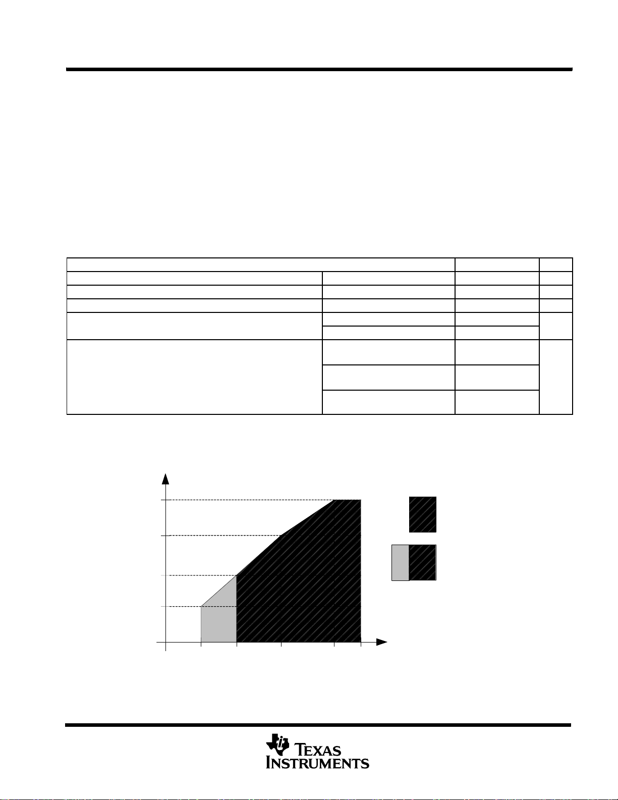
PARAMETER MIN MAX UNIT
Supply voltage during program execution, V
Supply voltage during flash memory programming, V
Supply voltage, V
Operatingfree-air temperature, T
Processor frequency f
(see Notes 2 and 3 and Figure 1)
NOTES: 1. It is recommended to power AVCCand DVCCfrom the s ame source. A maximum difference of 0.3 V between AVCCand DVCCcan
2. The MSP430 CPU is clocked directly with MCLK.
3. Modules might have a different maximum input clock specification. See the specification of the respective module in this data sheet.
SS
A
SYSYTEM
be tolerated during power-up.
Both the high and low phase of MCLK must not exceed the pulse width of the specified maximum frequency.
(maximum MCLK frequency)
CC
CC
AVCC=DVCC=VCC(see Note 1) 1.8 3.6 V
AVCC=DVCC=VCC(see Note 1) 2.2 3.6 V
AVSS=DVSS=V
I version -- 4 0 85
T v ersion -- 4 0 105
VCC=1.8V,
Duty cycle = 50% ± 10%
VCC=2.7V,
Duty cycle = 50% ± 10%
VCC≥ 3.3 V,
Duty cycle = 50% ± 10%
SS
--0.3 V to 4.1 V......................................................
+0.3V.......................................
CC
0.0 0.0 V
dc 4.15
dc 12
dc 16
MHz
°C
16 MHz
12 MHz
7.5 MHz
System Frequency -- MHz
4.15 MHz
1.8 V 2.2 V 2.7 V 3.3 V 3.6 V
NOTE: Minimum processor frequency is defined by system clock. Flash program or erase operations require a minimum VCCof 2.2 V.
Supply Voltage -- V
Legend:
Supply voltage range
during flash memory
programming
Supply voltage range
during program execution
Figure 1. Operating Area
POST OFFICE BOX 655303 • DALLAS, TEXAS 75265
29
Page 30
MSP430x241x, MSP430x261x
A
(
AM)
f
3
2,768
H
V
Activemode(AM
)
A
A
_
V
A
(
AM)
f
3
2,768
H
V
Activemode(AM
)
A
A
_
V
f
,
A
(
AM)
f
A
CLK
=32,768Hz/8=4,096Hz
g
V
Activemode(AM
)
Programexecutesinflas
h
ADIVMxDIVSxDIVAx11,
V
A
(
AM)
f
f
V
Activemode(AM
)
Programexecutesinflas
h
A
V
http://www.xinpian.net
提供单片机解密、IC解密、芯片解密业务
010-62245566 13810019655
MIXED SIGNAL MICROCONTROLLER
SLAS541A -- JUNE 2007 -- REVISED OCTOBER 2007
electrical characteristics over recommended ranges of supply voltage and operating free-air
temperature (unless otherwise noted)
active mode supply current into VCCexcluding external current (see Notes 1 and 2)
PARAMETER TEST CONDITIONS T
f
DCO=fMCLK=fSMCLK
=
ACLK
I
AM, 1MHz
I
AM, 1MHz
I
AM, 4kHz
I
AM,100kHz
NOTES: 1. All inputs are tied to 0 V or VCC. Outputs do not source or sink any current.
ctive mode
current (1 MHz)
ctive mode
current (1 MHz)
ctive mode
current (4 kHz)
ctive mode
current (100 kHz)
2. The currents are characterized with a micro crystal CC4V-T1A SMD crystal with a load capacitance of 9 pF. The internal and external
load capacitance is chosen to closely match the required 9 pF.
Program executes from flash,
BCSCTL1 = C
DCOCTL = CALDCO_1MHZ,
CPUOFF = 0, SCG0 = 0, SCG1 = 0,
OSCOFF = 0
f
DCO=fMCLK=fSMCLK
=
ACLK
Program executes in RAM,
BCSCTL1 = C
DCOCTL = CALDCO_1MHZ,
CPUOFF = 0, SCG0 = 0, SCG1 = 0,
OSCOFF = 0
f
MCLK=fSMCLK
=32,768 Hz/8=4,096 Hz
f
=0Hz,
DCO
Pro
ram executes inflash,
SELMx = 11, SELS = 1,
DIVMx = DIVSx = DIVAx = 11,
CPUOFF = 0, SCG0 = 1, SCG1 = 0,
OSCOFF = 0
f
MCLK=fSMCLK=fDCO(0, 0)
=0Hz,
ACLK
Program executes in
RSELx = 0, DCOx = 0,
CPUOFF = 0, SCG0 = 0, SCG1 = 0,
OSCOFF = 1
=1MHz,
z,
LBC1_1MHZ,
=1MHz,
z,
LBC1_1MHZ,
=
,
lash,
,
,
≈ 100 kHz,
-- 4 0 _Cto85_C
105_C
-- 4 0 _Cto85_C
105_C
-- 4 0 _Cto85_C
105_C
-- 4 0 _Cto85_C
105_C
-- 4 0 _Cto85_C
105_C
-- 4 0 _Cto85_C
105_C
-- 4 0 _Cto85_C
105_C
-- 4 0 _Cto85_C
105_C
A
VCC MIN TYP MAX UNIT
2.2
3
2.2
3
2.2
3
2.2
3
365 395
375 420
515 560
525 595
330 370
340 390
460 495
470 520
2.1 9
15 31
3 11
19 32
67 86
80 99
84 107
99 128
μ
μ
μ
μ
30
POST OFFICE BOX 655303 • DALLAS, TEXAS 75265
Page 31

MSP430x241x, MSP430x261x
http://www.xinpian.net
提供单片机解密、IC解密、芯片解密业务
010-62245566 13810019655
MIXED SIGNAL MICROCONTROLLER
SLAS541A -- JUNE 2007 -- REVISED OCTOBER 2007
electrical characteristics over recommended ranges of supply voltage and operating free-air
temperature (unless otherwise noted)
typical characteristics -- active mode supply current (into DVCC+AVCC)
10.0
9.0
8.0
7.0
6.0
5.0
4.0
3.0
Active Mode Current -- mA
2.0
1.0
0.0
1.5 2.0 2.5 3.0 3.5 4.0
f
=16MHz
DCO
f
=12MHz
DCO
f
=8MHz
DCO
f
=1MHz
DCO
VCC-- Supply Voltage -- V
Figure 2. Active Mode Current vs VCC,TA=25°C
7.0
TA=85°C
6.0
5.0
4.0
3.0
2.0
Active Mode Current -- mA
1.0
0.0
0.0 4.0 8.0 12.0 16.0
VCC=3V
f
DCO
TA=85°C
TA=25°C
VCC=2.2V
-- DCO Frequency -- MHz
TA=25°C
Figure 3. Active Mode Current vs DCO Frequency
POST OFFICE BOX 655303 • DALLAS, TEXAS 75265
31
Page 32

MSP430x241x, MSP430x261x
f
f
1MH
V
A
A
_
V
f
f
f
ACLK
V
I
LPM
0
f
ACL
K
=0H
z
AseeNote3
V
f
A
V
BCSCTL1=CALBC1_1MHZ
AseeNote4
V
V
f
f
f
0MH
f
f
ACL
K
=32,768Hz
AseeNote4
V
V
f
f
f
0MH
f
f
(
VLO)
Low-powermode
3
f
ACL
K
frominternalLFoscillator(VLO)
A()
V
http://www.xinpian.net
提供单片机解密、IC解密、芯片解密业务
010-62245566 13810019655
MIXED SIGNAL MICROCONTROLLER
SLAS541A -- JUNE 2007 -- REVISED OCTOBER 2007
electrical characteristics over recommended ranges of supply voltage and operating free-air
temperature (unless otherwise noted)
low-power mode supply current into VCCexcluding external current (see Notes 1 and 2)
PARAMETER TEST CONDITIONS T
f
=0MHz,
I
LPM0, 1MHz
Low-power mode 0
(LPM0) current,
seeNote3
MCLK
=
=
SMCLK
f
ACLK
DCO
= 32,768 Hz,
BCSCTL1 = C
z,
LBC1_1MHZ,
DCOCTL = CALDCO_1MHZ,
-- 4 0 _Cto85_C
-- 4 0 _Cto85_C
CPUOFF = 1, SCG0 = 0, SCG1 = 0,
OSCOFF = 0
f
=0MHz,
I
100kHz
MCLK
=
,
Low-power mode 0
(LPM0) current,
seeNote3
SMCLK
RSELx = 0, DCOx = 0,
CPUOFF = 1, SCG0 = 0, SCG1 = 0,
DCO(0, 0)
=0Hz,
≈ 100 kHz,
,
-- 4 0 _Cto85_C
-- 4 0 _Cto85_C
OSCOFF = 1
I
LPM2
Low-power mode 2
(LPM2) current,
seeNote4
f
MCLK=fSMCLK
= 32,768 Hz,
ACLK
BCSCTL1 = C
DCOCTL = CALDCO_1MHZ,
CPUOFF = 1, SCG0 = 0, SCG1 = 1,
=0MHz,f
DCO
LBC1_1MHZ,
=1MHz,
,
-- 4 0 _Cto85_C
-- 4 0 _Cto85_C
OSCOFF = 0
=
I
LPM3,LFXT1
Low-power mode 3
(LPM3) current,
MCLK
=
DCO
= 32,768 Hz,
CPUOFF = 1, SCG0 = 1, SCG1 = 1,
SMCLK
,
=
z,
OSCOFF = 0
=
I
LPM3,VLO
Low-power mode 3
(LPM3) current,
MCLK
=
DCO
rom i nternal LF oscillator
CPUOFF = 1, SCG0 = 1, SCG1 = 1,
SMCLK
=
z,
,
,
seeNote4 OSCOFF=0
NOTES: 1. All inputs are tied to 0 V or VCC. Outputs do not source or sink any current.
2. The currents are characterized with a micro crystal CC4V-T1A SMD crystal with a load capacitance of 9 pF. The internal and external
load capacitance is chosen to closely match the required 9 pF.
3. Current for Brownout and WDT+ is included. The WDT+ is clocked by SMCLK.
4. Current for Brownout and WDT+ is included. The WDT+ is clocked by ACLK.
A
105_C
105_C
105_C
105_C
105_C
105_C
-- 4 0 °C 0.8 1.2
25°C
85°C
105°C 14 24
-- 4 0 °C 0.9 1.3
25°C
85°C
105°C 17 30
-- 4 0 °C 0.4 1.0
25°C
85°C
105°C 14 24
-- 4 0 °C 0.6 1.2
25°C
85°C
105°C 16.5 29.5
VCC MIN TYP MAX UNIT
68 83
2.2
83 98
μ
87 105
3
100 125
2.2
3
2.2
3
2.2
37 49
50 62
40 55
57 73
23 33
35 46
25 36
40 55
1 1.3
4.6 7
μ
μ
μ
3
2.2
1.1 1.5
5.5 8
0.5 1.0
4.3 6.5
μ
3
0.6 1.2
5 7.5
32
POST OFFICE BOX 655303 • DALLAS, TEXAS 75265
Page 33

MSP430x241x, MSP430x261x
L
(
f
f
f
0MH
f
(LPM4)current
f
ACL
K
=0H
z
A
L
(
f
f
f
0MH
f
(LPM4)current
f
ACL
K
=0H
z
A
http://www.xinpian.net
提供单片机解密、IC解密、芯片解密业务
010-62245566 13810019655
MIXED SIGNAL MICROCONTROLLER
SLAS541A -- JUNE 2007 -- REVISED OCTOBER 2007
electrical characteristics over recommended ranges of supply voltage and operating free-air
temperature (unless otherwise noted)
low-power mode supply current into VCCexcluding external current (see Notes 1 and 2) (continued)
PARAMETER TEST CONDITIONS T
ow-power mode4
I
LPM4
I
LPM4
NOTES: 1. All inputs are tied to 0 V or VCC. Outputs do not source or sink any current.
LPM4)current,
seeNote3
ow-power mode4
LPM4)current,
seeNote3
2. The currents are characterized with a micro crystal CC4V--T1A SMD crystal with a load capacitance of 9 pf. The internal and external
load capacitance is chosen to closely match the required 9 pf.
3. Current for Brownout included.
,
,
=
MCLK
=0Hz,
=
MCLK
=0Hz,
=
,
=
,
DCO
CPUOFF = 1, SCG0 = 1, SCG1 = 1,
OSCOFF = 1
DCO
CPUOFF = 1, SCG0 = 1, SCG1 = 1,
OSCOFF = 1
SMCLK
SMCLK
=
z,
=
z,
typical characteristics -- LPM4 current
A
-- 4 0 °C 0.1 0.5
25°C
85°C
105°C 13 23
-- 4 0 °C 0.2 0.5
25°C
85°C
105°C 14 24
VCC MIN TYP MAX UNIT
2.2 V
3V
0.1 0.5
4 6
0.2 0.5
4.7 7
μ
μ
16.0
15.0
14.0
13.0
12.0
11.0
10.0
9.0
8.0
7.0
6.0
5.0
4.0
ILPM4 -- Low-- power mode current -- uA
ILPM4 -- Low-- power mode current --
3.0
2.0
1.0
0.0
Figure 4. I
Vcc = 3.6V
Vcc = 3.0V
Vcc = 2.2V
Vcc = 1.8V
--40.0 --20.0 0.0 20.0 40.0 60.0 80.0 100.0 120.0
TA-- Temperature -- °C
TA-- Temperature -- °C
-- LPM4 Current vs Temperature
LPM4
POST OFFICE BOX 655303 • DALLAS, TEXAS 75265
33
Page 34

MSP430x241x, MSP430x261x
V
IT+
Positivegoinginputthresholdvoltag
e
V
V
I
T
Negativegoinginputthresholdvoltag
e
V
V
http://www.xinpian.net
提供单片机解密、IC解密、芯片解密业务
010-62245566 13810019655
MIXED SIGNAL MICROCONTROLLER
SLAS541A -- JUNE 2007 -- REVISED OCTOBER 2007
Schmitt-trigger inputs -- ports P1 through P8, RST/NMI, JTAG, XIN, and XT2IN (see Note 4)
PARAMETER TEST CONDITIONS VCC MIN TYP MAX UNIT
0.45 V
CC
V
Positive-going input threshold voltage
IT+
2.2 V 1.0 1.65
3V 1.35 2.25
0.25 V
CC
V
Negative-going input threshold voltage
IT--
--
2.2 V 0.55 1.2
3V 0.75 1.65
V
Input voltage hysteresis (V
hys
R
Pullup/pulldown resistor
Pull
C
Input capacitance VIN=VSSor V
I
IT+
-- V
IT--
)
Pullup: VIN=VSS,
Pulldown: VIN=V
CC
CC
2.2 V 0.2 1.0
3V 0.3 1.0
20 35 50 kΩ
NOTE 4: XIN and XT2IN in bypass mode only.
inputs -- ports P1 and P2
PARAMETER TEST CONDITIONS VCC MIN MAX UNIT
t
External interrupt timing
int
NOTE: The external signal sets the interrupt flag every time the minimum t
than t
(int)
.
Port P1, P2: P1.x to P2.x, external trigger pulse width to
set the interrupt flag (see Note)
parameters are met. It may be set even with trigger signals shorter
(int)
2.2 V/3 V 20 ns
leakage current -- ports P1 through P8 (see Note 1 and 2)
PARAMETER TEST CONDITIONS VCC MIN MAX UNIT
I
lkg (Px.x)
NOTES: 1. The leakage current is measured with VSSor VCCapplied to the corresponding pin(s), unless otherwise noted.
High-impedance leakage current see Notes 1 and 2 2.2 V/3 V ±50 nA
2. The leakage of digital port pins is measured individually. The port pin is selected for input and the pull--up/pull--down resistor is
disabled..
0.75 V
0.55 V
5 pF
CC
V
CC
V
34
POST OFFICE BOX 655303 • DALLAS, TEXAS 75265
Page 35

MSP430x241x, MSP430x261x
V
V
V
V
f
Portoutputfrequency
P1.4/SMCLK,
CL20pF,
RL1
k
Ω
f
P2.0/ACLK/CA2,P1.4/SMCLK,
CL20p
F
%
Dutycycleofoutput
q
y
http://www.xinpian.net
提供单片机解密、IC解密、芯片解密业务
010-62245566 13810019655
MIXED SIGNAL MICROCONTROLLER
SLAS541A -- JUNE 2007 -- REVISED OCTOBER 2007
electrical characteristics over recommended ranges of supply voltage and operating free-air
temperature (unless otherwise noted) (continued)
standard inputs -- RST/NMI
PARAMETER TEST CONDITIONS VCC MIN MAX UNIT
V
V
outputs -- ports P1 through P8
V
V
NOTES: 1. The maximum total current, I
Low-level input voltage 2.2 V/3 V VSSVSS+0.6 V
IL
High-level input voltage 2.2 V/3 V 0.8×V
IH
CC
PARAMETER TEST CONDITIONS VCC MIN MAX UNIT
OH
OL
High-level output voltage
Low-level output voltage
OH(max)
I
I
I
I
I
I
I
I
and I
= --1.5 mA (see Note 2)
OH(max)
= --6 mA (see Note 2)
OH(max)
= --1.5 mA (see Note 2)
OH(max)
= --6 mA (see Note 2)
OH(max)
= 1.5 mA (see Note 2)
OL(max)
= 6 mA (see Note 2)
OL(max)
= 1.5 mA (see Note 2)
OL(max)
= 6 mA (see Note 2)
OL(max)
for all outputs combined, should not exceed ±12 mA to satisfy the maximum
OL(max),
VCC--0.25 V
2.2 V
VCC--0.25 V
3
2.2 V
3
VCC-- 0 . 6 V
VCC-- 0 . 6 V
VSSVSS+0.25
V
SSVSS
VSSVSS+0.25
V
SSVSS
voltage drop specified.
2. The maximum total current, I
OH(max)
and I
for all outputs combined, should not exceed ±48 mA to satisfy the maximum
OL(max),
voltage drop specified.
V
CC
CC
CC
CC
CC
+0.6
+0.6
V
output frequency -- ports P1 through P8
PARAMETER TEST CONDITIONS VCC MIN TYP MAX UNIT
Px.y
Port_CLK
with load
Clock outputfrequency
(see Notes 1 and 2)
P2.0/ACLK/CA2, P1.4/SMCLK, CL=20pF
(see Note 2)
P5.6/ACLK, CL= 20 pF, LF mode 30 50 70
P5.6/ACLK, CL=20pF,XT1mode 40 50 60
Port output frequency P1.4/SMCLK, CL=20pF,RL=1kΩ
t
(Xdc)
Duty cycle of output
frequency
P5.4/MCLK, C
P5.4/MCLK, C
=20pF,XT1mode 40 60
L
= 20 pF, DCO 50% -- 15 ns 50% 50% + 15 ns
L
P1.4/SMCLK, CL=20pF,XT2mode 40 60 %
P1.4/SMCLK, CL= 20 pF, DCO 50% -- 15 ns 50% + 15 ns
NOTES: 1. A resistive divider with 2 times 0.5 kΩ between VCCand VSSis used as load. The output is connected to the center tap of the divider.
2. The output voltage reaches at least 10% and 90% V
at the specified toggle frequency.
CC
2.2 V DC 10
3.0 V DC 12
2.2 V DC 12
3.3 V DC 16
MHz
MHz
%
POST OFFICE BOX 655303 • DALLAS, TEXAS 75265
35
Page 36

MSP430x241x, MSP430x261x
A
A
http://www.xinpian.net
提供单片机解密、IC解密、芯片解密业务
010-62245566 13810019655
MIXED SIGNAL MICROCONTROLLER
SLAS541A -- JUNE 2007 -- REVISED OCTOBER 2007
electrical characteristics over recommended ranges of supply voltage and operating free-air
temperature (unless otherwise noted) (continued)
typical characteristics -- outputs
TYPICALLOW-LEVEL OUTPUT CURRENT
vs
LOW-LEVEL OUTPUT VOLTAGE
of one pin
25.0
VCC=2.2V
P4.5
20.0
15.0
10.0
5.0
OL
I -- Typical Low-Level Output Current -- m
0.0
0.0 0.5 1.0 1.5 2.0 2.5
VOL-- Low-Level Output Voltage -- V
TA=25°C
TA=85°C
Figure 5
TYPICAL HIGH-LEVEL OUTPUT CURRENT
vs
HIGH-LEVEL OUTPUT VOLTAGE
of one pin
0.0
VCC=2.2V
P4.5
-- 5 . 0
TYPICALLOW-LEVEL OUTPUT CURRENT
vs
LOW-LEVEL OUTPUT VOLTAGE
of one pin
50.0
VCC=3V
P4.5
40.0
30.0
20.0
10.0
OL
I -- Typical Low-Level Output Current -- mA
0.0
0.0 0.5 1.0 1.5 2.0 2.5 3.0 3.5
VOL-- Low-Level Output Voltage -- V
Figure 6
TYPICAL HIGH-LEVEL OUTPUT CURRENT
vs
HIGH-LEVEL OUTPUT VOLTAGE
of one pin
0.0
VCC=3V
P4.5
--10.0
TA=25°C
TA=85°C
--10.0
--15.0
TA=85°C
TA=25°C
0.0 0.5 1.0 1.5 2.0 2.5
VOH-- High-Level Output Voltage -- V
OH
I -- Typical High-Level Output Current -- m
--20.0
--25.0
Figure 7
36
--20.0
--30.0
TA=85°C
--40.0
OH
I -- Typical High-Level Output Current -- mA
--50.0
0.0 0.5 1.0 1.5 2.0 2.5 3.0 3.5
POST OFFICE BOX 655303 • DALLAS, TEXAS 75265
TA=25°C
VOH-- High-Level Output Voltage -- V
Figure 8
Page 37

MSP430x241x, MSP430x261x
http://www.xinpian.net
提供单片机解密、IC解密、芯片解密业务
010-62245566 13810019655
MIXED SIGNAL MICROCONTROLLER
SLAS541A -- JUNE 2007 -- REVISED OCTOBER 2007
electrical characteristics over recommended ranges of supply voltage and operating free-air
temperature (unless otherwise noted) (continued)
POR/brownout reset (BOR) (see Notes 1 and 2)
PARAMETER TEST CONDITIONS VCC MIN TYP MAX UNIT
V
CC(start)
V
(B_IT--)
V
hys(B_IT--)VCC
t
d(BOR)
t
reset
NOTES: 1. The current consumption of the brownout module is i ncluded in the ICCcurrent consumption data. The voltage level
operating voltage dVCC/dt ± 3V/s 0.7 ¢ V
(B_IT--)
negative going VCCreset threshold voltage dVCC/dt ± 3V/s 1.71 V
reset threshold hysteresis dVCC/dt ± 3V/s 70 130 210 mV
BOR reset release delay time 2000 μs
Pulse length at RST/NMI pin to accept a reset 2.2 V / 3 V 2 μs
V
(B_IT--)+Vhys(B_IT--)
2. During power up, the CPU begins code execution following a period of t
settings must not be changed until V
is ≤ 1.8 V.
CC
≥ V
CC(MIN)
, where V
after VCC=V
d(BOR)
is the minimum supply voltage for the desired operating
CC(min)
(B_IT--)+Vhys(B_IT--)
. The default DCO
frequency.
V
CC
V
hys(B_IT-)
V
(B_IT-)
V
V
CC(Start)
1
0
t
d(BOR)
Figure 9. POR/Brownout Reset (BOR) vs Supply Voltage
POST OFFICE BOX 655303 • DALLAS, TEXAS 75265
37
Page 38

MSP430x241x, MSP430x261x
http://www.xinpian.net
提供单片机解密、IC解密、芯片解密业务
010-62245566 13810019655
MIXED SIGNAL MICROCONTROLLER
SLAS541A -- JUNE 2007 -- REVISED OCTOBER 2007
electrical characteristics over recommended ranges of supply voltage and operating free-air
temperature (unless otherwise noted) (continued)
typical characteristics -- POR/brownout reset (BOR)
V
2
1.5
-- V
1
=3V
V
CC
Typical Conditions
CC
3V
t
pw
CC(drop)
V
0.5
0
0.001 1 1000
tpw-- Pulse Width -- μs
Figure 10. V
2
V
Typical Conditions
1.5
-- V
1
CC(drop)
V
0.5
0
0.001 1 1000
Figure 11. V
CC
=3V
CC(drop)
t
pw
CC(drop)
Level With a Square Voltage Drop to Generate a POR/Brownout Signal
-- Pulse Width -- μs
Level With a Triangle Voltage Drop to Generate a POR/Brownout Signal
V
V
CC(drop)
CC(drop)
V
CC
3V
1ns 1ns
tpw-- Pulse Width -- μs
t
pw
tf=t
r
t
f
tpw-- Pulse Width -- μs
t
r
38
POST OFFICE BOX 655303 • DALLAS, TEXAS 75265
Page 39
MSP430x241x, MSP430x261x
)
V
hys(SVS_I
T--)
/
V
V
http://www.xinpian.net
提供单片机解密、IC解密、芯片解密业务
010-62245566 13810019655
MIXED SIGNAL MICROCONTROLLER
SLAS541A -- JUNE 2007 -- REVISED OCTOBER 2007
electrical characteristics over recommended ranges of supply voltage and operating free-air
temperature (unless otherwise noted) (continued)
SVS (supply voltage supervisor/monitor)
PARAMETER TEST CONDITIONS MIN TYP MAX UNIT
t
(SVSR)
t
d(SVSon)
t
settle
V
(SVSstart)
V
hys(SVSIT--
(SVS_IT--)
I
CC(SVS)
(see Note 1)
†
The recommended operating voltage range is limited to 3.6 V.
‡
t
is the settling time that the comparator o/p needs to have a stable level after VLD is switched VLD ≠ 0 to a different VLD value somewhere
settle
between 2 and 15. The overdrive is assumed to be > 50 mV.
NOTE 1: The current consumption of the SVS module is not included in the I
dVCC/dt > 30 V/ms (see Figure 12) 5 150
dVCC/dt ≤ 30 V/ms 2000
μs
SVSON, switch from VLD = 0 to VLD ≠ 0, VCC=3V 20 150 μs
‡
VLD ≠ 0
12 μs
VLD ≠ 0, VCC/dt ≤ 3 V/s (see Figure 12) 1.55 1.7 V
VLD = 1 70 120 210 mV
VCC/dt ≤ 3 V/s (see Figure 12)
VCC/dt ≤ 3 V/s (see Figure 12), External voltage applied
on A7
VLD=2to14
VLD = 15 4.4 20 mV
V
(SVS_IT--)
0.004
×
V
(SVS_IT--)
×
0.016
VLD = 1 1.8 1.9 2.05
VLD = 2 1.94 2.1 2.25
VLD = 3 2.05 2.2 2.37
VLD = 4 2.14 2.3 2.48
VLD = 5 2.24 2.4 2.6
VLD = 6 2.33 2.5 2.71
V
dt ≤ 3V/s (see Figure 12 and Figure 13)
CC
VLD = 7 2.46 2.65 2.86
VLD = 8 2.58 2.8 3
VLD = 9 2.69 2.9 3.13
VLD = 10 2.83 3.05 3.29
VLD = 11 2.94 3.2 3.42
3.99
†
†
†
VCC/dt ≤ 3 V/s (see Figure 12 and Figure 13),
External voltage applied on A7
VLD = 12 3.11 3.35 3.61
VLD = 13 3.24 3.5 3.76
VLD = 14 3.43 3.7
†
VLD = 15 1.1 1.2 1.3
VLD ≠ 0, VCC=2.2V/3V 10 15 μA
current consumption data.
CC
V
POST OFFICE BOX 655303 • DALLAS, TEXAS 75265
39
Page 40

MSP430x241x, MSP430x261x
http://www.xinpian.net
提供单片机解密、IC解密、芯片解密业务
010-62245566 13810019655
MIXED SIGNAL MICROCONTROLLER
SLAS541A -- JUNE 2007 -- REVISED OCTOBER 2007
typical characteristics
AV
V
(SVS_IT--)
V
(SVSstart)
V
(B_IT--)
V
CC(start)
Brownout
SVS out
CC
1
0
1
V
hys(SVS_IT--)
V
hys(B_IT--)
Brownout
Region
t
d(BOR)
Software sets VLD >0:
SVS is active
SVS Circuit is Active From VLD > to VCC<V(
B_IT-- )
Brown-
out
Region
t
d(BOR)
Set POR
1.5
-- V
CC(min)
V
0.5
0
1
undefined
0
t
d(SVSon)
Figure 12. SVS Reset (SVSR) vs Supply Voltage
2
Rectangular Drop
Triangular Drop
1
0
1 10 1000
-- Pulse Width -- μs
t
pw
100
V
CC(min)
V
CC(min)
V
V
3V
CC
3V
CC
t
d(SVSR)
t
pw
1ns 1ns
t
pw
Figure 13. V
40
CC(min)
: Square Voltage Drop and Triangle Voltage Drop to Generate an SVS Signal (VLD = 1)
POST OFFICE BOX 655303 • DALLAS, TEXAS 75265
tf=t
r
t
f
t -- Pulse Width -- μs
t
r
Page 41
MSP430x241x, MSP430x261x
VccSupplyvoltagerange
V
http://www.xinpian.net
提供单片机解密、IC解密、芯片解密业务
010-62245566 13810019655
MIXED SIGNAL MICROCONTROLLER
SLAS541A -- JUNE 2007 -- REVISED OCTOBER 2007
electrical characteristics over recommended ranges of supply voltage and operating free-air
temperature (unless otherwise noted) (continued)
main DCO characteristics
D All r anges selected by RSELx overlap with RSELx + 1: RSELx = 0 overlaps RSELx = 1, ... RSELx = 14
overlaps RSELx = 15.
D DCO control bits DCOx have a step size as defined by parameter S
D Modulation control bits MODx select how often f
cycles. The frequency f
to:
DCO(RSEL,DCO)
is used for the remaining cycles. The frequency is an average equal
DCO(RSEL,DCO+1)
is used within the period of 32 DCOCLK
DCO
.
f
average
=
MOD × f
32 × f
DCO(RSEL,DCO)
DCO(RSEL,DCO)
× f
DCO(RSEL,DCO+1)
+(32−MOD) × f
DCO(RSEL,DCO+1)
DCO frequency
PARAMETER TEST CONDITIONS VCC MIN TYP MAX UNIT
RSELx < 14 1.8 3.6
Vcc Supply voltage range
f
DCO(0,0)
f
DCO(0,3)
f
DCO(1,3)
f
DCO(2,3)
f
DCO(3,3)
f
DCO(4,3)
f
DCO(5,3)
f
DCO(6,3)
f
DCO(7,3)
f
DCO(8,3)
f
DCO(9,3)
f
DCO(10,3)
f
DCO(11,3)
f
DCO(12,3)
f
DCO(13,3)
f
DCO(14,3)
f
DCO(15,3)
f
DCO(15,7)
S
RSEL
S
DCO
Duty cycle Measured at P1.4/SMCLK 2.2 V/3 V 40 50 60 %
DCO frequency (0, 0) RSELx = 0, DCOx = 0, MODx = 0 2.2 V/3 V 0.06 0.14 MHz
DCO frequency (0, 3) RSELx = 0, DCOx = 3, MODx = 0 2.2 V/3 V 0.07 0.17 MHz
DCO frequency (1, 3) RSELx = 1, DCOx = 3, MODx = 0 2.2 V/3 V 0.10 0.20 MHz
DCO frequency (2, 3) RSELx = 2, DCOx = 3, MODx = 0 2.2 V/3 V 0.14 0.28 MHz
DCO frequency (3, 3) RSELx = 3, DCOx = 3, MODx = 0 2.2 V/3 V 0.20 0.40 MHz
DCO frequency (4, 3) RSELx = 4, DCOx = 3, MODx = 0 2.2 V/3 V 0.28 0.54 MHz
DCO frequency (5, 3) RSELx = 5, DCOx = 3, MODx = 0 2.2 V/3 V 0.39 0.77 MHz
DCO frequency (6, 3) RSELx = 6, DCOx = 3, MODx = 0 2.2 V/3 V 0.54 1.06 MHz
DCO frequency (7, 3) RSELx = 7, DCOx = 3, MODx = 0 2.2 V/3 V 0.80 1.50 MHz
DCO frequency (8, 3) RSELx = 8, DCOx = 3, MODx = 0 2.2 V/3 V 1.10 2.10 MHz
DCO frequency (9, 3) RSELx = 9, DCOx = 3, MODx = 0 2.2 V/3 V 1.60 3.00 MHz
DCO frequency (10, 3) RSELx = 10, DCOx = 3, MODx = 0 2.2 V/3 V 2.50 4.30 MHz
DCO frequency (11, 3) RSELx = 11, DCOx = 3, MODx = 0 2.2 V /3 V 3.00 5.50 MHz
DCO frequency (12, 3) RSELx = 12, DCOx = 3, MODx = 0 2.2 V/3 V 4.30 7.30 MHz
DCO frequency (13, 3) RSELx = 13, DCOx = 3, MODx = 0 2.2 V/3 V 6.00 9.60 MHz
DCO frequency (14, 3) RSELx = 14, DCOx = 3, MODx = 0 2.2 V/3 V 8.60 13.9 MHz
DCO frequency (15, 3) RSELx = 15, DCOx = 3, MODx = 0 3V 12.0 18.5 MHz
DCO frequency (15, 7) RSELx = 15, DCOx = 7, MODx = 0 3V 16.0 26.0 MHz
Frequency step between
range RSEL and RSEL+1
Frequency step between
tap DCO and DCO+1
RSELx = 14
RSELx = 15 3.0 3.6
S
RSEL=fDCO(RSEL+1,DCO)/fDCO(RSEL,DCO)
S
DCO=fDCO(RSEL,DCO+1)/fDCO(RSEL,DCO)
2.2 V/3 V 1.55 ratio
2.2 V/3 V 1.05 1.08 1.12 ratio
2.2 3.6
V
POST OFFICE BOX 655303 • DALLAS, TEXAS 75265
41
Page 42

MSP430x241x, MSP430x261x
)
BCSCTL1=CALBC1_1MHz
f
CAL(1MHz)
1MHzcalibrationvalueDCOCTLCALDCO_1MHz
,
0Cto85C
MHz
)
BCSCTL1=CALBC1_8MHz
f
CAL(8MHz)
8MHzcalibrationvalueDCOCTLCALDCO_8MHz
,
0Cto85C
MHz
)
BCSCTL1=CALBC1_12MH
z
f
CAL(12MHz
)
12MHzcalibrationvalueDCOCTLCALDCO_12MHz
,
0Cto85C
MHz
f
http://www.xinpian.net
提供单片机解密、IC解密、芯片解密业务
010-62245566 13810019655
MIXED SIGNAL MICROCONTROLLER
SLAS541A -- JUNE 2007 -- REVISED OCTOBER 2007
electrical characteristics over recommended ranges of supply voltage and operating free-air
temperature (unless otherwise noted) (continued)
calibrated DCO frequencies -- tolerance at calibration
PARAMETER TEST CONDITIONS T
A
Frequency tolerance at calibration 25°C 3V -- 1 ±0.2 +1 %
BCSCTL1 = CALBC1_1MHz,
f
CAL(1MHz)
1-MHz calibration value
DCOCTL = CALDCO_1MHz,
25°C 3V 0.990 1 1.010 MHz
Gating time: 5 ms
BCSCTL1 = CALBC1_8MHz,
f
CAL(8MHz)
8-MHz calibration value
DCOCTL = CALDCO_8MHz,
25°C 3V 7.920 8 8.080 MHz
Gating time: 5ms
BCSCTL1 = CALBC1_12MHz,
f
CAL(12MHz)
12-MHz calibration value
DCOCTL = CALDCO_12MHz,
25°C 3V 11. 8 8 12 12.12 MHz
Gating time: 5ms
BCSCTL1 = CALBC1_16MHz,
f
CAL(16MHz)
16-MHz calibration value
DCOCTL = CALDCO_16MHz,
25°C 3V 15.84 16 16.16 MHz
Gating time: 2 ms
calibrated DCO frequencies -- tolerance over temperature 0°Cto85°C
PARAMETER TEST CONDITIONS T
1-MHz tolerance over temperature 0°Cto85°C 3V -- 2 . 5 ±0.5 +2.5 %
8-MHz tolerance over temperature 0°Cto85°C 3V -- 2 . 5 ±1.0 +2.5 %
12-MHz tolerance over temperature 0°Cto85°C 3V -- 2 . 5 ±1.0 +2.5 %
16-MHz tolerance over temperature 0°Cto85°C 3V -- 3 . 0 ±2.0 +3.0 %
f
CAL(1MHz
f
CAL(8MHz
f
CAL(12MHz
1-MHz calibration value
8-MHz calibration value
12-MHz calibration value
DCOCTL = CALDCO_1MHz,
=
Gating time: 5ms
=
DCOCTL = CALDCO_8MHz,
Gating time: 5 ms
=
DCOCTL = CALDCO_12MHz,
Gating time: 5 ms
,
,
,
BCSCTL1 = CALBC1_16MHz,
CAL(16MHz)
16-MHz calibration value
DCOCTL = CALDCO_16MHz,
Gating time: 2 ms
A
0°Cto85°C
0°Cto85°C
0°Cto85°C
0°Cto85°C
VCC MIN TYP MAX UNIT
VCC MIN TYP MAX UNIT
2.2 V 0.970 1 1.030
3V 0.975 1 1.025
MHz
3.6 V 0.970 1 1.030
2.2 V 7.760 8 8.400
3V 7.800 8 8.200
MHz
3.6 V 7.600 8 8.240
2.2 V 11.6 4 12 12.36
3V 11.64 12 12.36
MHz
3.6 V 11.6 4 12 12.36
3V 15.52 16 16.48
3.6 V 15.00 16 16.48
MHz
42
POST OFFICE BOX 655303 • DALLAS, TEXAS 75265
Page 43

MSP430x241x, MSP430x261x
http://www.xinpian.net
提供单片机解密、IC解密、芯片解密业务
010-62245566 13810019655
MIXED SIGNAL MICROCONTROLLER
SLAS541A -- JUNE 2007 -- REVISED OCTOBER 2007
electrical characteristics over recommended ranges of supply voltage and operating free-air
temperature (unless otherwise noted) (continued)
calibrated DCO frequencies -- tolerance over supply voltage V
PARAMETER
1-MHz tolerance over V
8-MHz tolerance over V
12-MHz tolerance over V
16-MHz tolerance over V
f
CAL(1MHz)
f
CAL(8MHz)
f
CAL(12MHz)
f
CAL(16MHz)
1-MHz calibration value
8-MHz calibration value
12-MHz calibration value
16-MHz calibration value
CC
CC
CC
CC
TEST CONDITIONS T
BCSCTL1 = CALBC1_1MHz,
DCOCTL = CALDCO_1MHz,
Gating time: 5 ms
BCSCTL1 = CALBC1_8MHz,
DCOCTL = CALDCO_8MHz,
Gating time: 5 ms
BCSCTL1 = CALBC1_12MHz,
DCOCTL = CALDCO_12MHz,
Gating time: 5 ms
BCSCTL1 = CALBC1_16MHz,
DCOCTL = CALDCO_16MHz,
Gating time: 2 ms
CC
A
25°C 1.8 V to 3.6 V -- 3 ±2 +3 %
25°C 1.8 V to 3.6 V -- 3 ±2 +3 %
25°C 2.2 V to 3.6 V -- 3 ±2 +3 %
25°C 3.0 V to 3.6 V -- 6 ±2 +3 %
25°C 1.8 V to 3.6 V 0.970 1 1.030 MHz
25°C 1.8 V to 3.6 V 7.760 8 8.240 MHz
25°C 2.2 V to 3.6 V 11.6 4 12 12.36 MHz
25°C 3.0 V to 3.6 V 15.00 16 16.48 MHz
VCC MIN TYP MAX UNIT
calibrated DCO frequencies -- overall tolerance
PARAMETER TEST CONDITIONS T
1-MHz tolerance overall -- 4 0 °C to 105°C 1.8 V to 3.6 V -- 5 ±2 +5 %
8-MHz tolerance overall -- 4 0 °C to 105°C 1.8 V to 3.6 V -- 5 ±2 +5 %
12-MHz tolerance overall -- 4 0 °C to 105°C 2.2 V to 3.6 V -- 5 ±2 +5 %
16-MHz tolerance overall -- 4 0 °C to 105°C 3Vto3.6V -- 6 ±3 +6 %
BCSCTL1 = CALBC1_1MHz,
f
CAL(1MHz)
f
CAL(8MHz)
f
CAL(12MHz)
f
CAL(16MHz)
1-MHz calibration value
8-MHz calibration value
12-MHz calibration value
16-MHz calibration value
DCOCTL = CALDCO_1MHz,
Gating time: 5ms
BCSCTL1 = CALBC1_8MHz,
DCOCTL = CALDCO_8MHz,
Gating time: 5ms
BCSCTL1 = CALBC1_12MHz,
DCOCTL = CALDCO_12MHz,
Gating time: 5ms
BCSCTL1 = CALBC1_16MHz,
DCOCTL = CALDCO_16MHz,
Gating time: 2 ms
A
-- 4 0 °C to 105°C 1.8 V to 3.6 V 0.950 1 1.050 MHz
-- 4 0 °C to 105°C 1.8 V to 3.6 V 7.600 8 8.400 MHz
-- 4 0 °C to 105°C 2.2 V to 3.6 V 11.40 12 12.60 MHz
-- 4 0 °C to 105°C 3Vto3.6V 15.00 16 17.00 MHz
VCC MIN TYP MAX UNIT
POST OFFICE BOX 655303 • DALLAS, TEXAS 75265
43
Page 44
MSP430x241x, MSP430x261x
http://www.xinpian.net
提供单片机解密、IC解密、芯片解密业务
010-62245566 13810019655
MIXED SIGNAL MICROCONTROLLER
SLAS541A -- JUNE 2007 -- REVISED OCTOBER 2007
electrical characteristics over recommended ranges of supply voltage and operating free-air
temperature (unless otherwise noted) (continued)
typical characteristics -- calibrated 1-MHz DCO frequency
1.02
1.01
TA= 105 °C
1.00
Frequency -- MHz
0.99
0.98
1.5 2.0 2.5 3.0 3.5 4.0
VCC-- Supply Voltage -- V
Figure 14. Calibrated 1-MHz Frequency vs V
typical characteristics -- calibrated 8-MHz DCO frequency
8.20
8.15
8.10
8.05
8.00
TA=25°C
TA= 105 °C
TA=85°C
TA=25°C
TA=--40°C
CC
TA=85°C
44
7.95
Frequency -- MHz
7.90
7.85
7.80
1.5 2.0 2.5 3.0 3.5 4.0
VCC-- Supply Voltage -- V
TA=--40°C
Figure 15. Calibrated 8-MHz Frequency vs V
POST OFFICE BOX 655303 • DALLAS, TEXAS 75265
CC
Page 45

MSP430x241x, MSP430x261x
http://www.xinpian.net
提供单片机解密、IC解密、芯片解密业务
010-62245566 13810019655
MIXED SIGNAL MICROCONTROLLER
SLAS541A -- JUNE 2007 -- REVISED OCTOBER 2007
electrical characteristics over recommended ranges of supply voltage and operating free-air
temperature (unless otherwise noted) (continued)
typical characteristics -- calibrated 12-MHz DCO frequency
12.2
12.1
12.0
11.9
Frequency -- MHz
11.8
11.7
1.5 2.0 2.5 3.0 3.5 4.0
VCC-- Supply Voltage -- V
TA=--40°C
TA=25°C
TA=85°C
Figure 16. Calibrated 12-MHz Frequency vs V
typical characteristics -- calibrated 16-MHz DCO frequency
16.1
TA= 105 °C
CC
16.0
TA=--40°C
15.9
15.8
Frequency -- MHz
15.7
15.6
1.5 2.0 2.5 3.0 3.5 4.0
VCC-- Supply Voltage -- V
TA=25°C
TA=85°C
TA= 105 °C
Figure 17. Calibrated 16-MHz Frequency vs V
POST OFFICE BOX 655303 • DALLAS, TEXAS 75265
CC
45
Page 46

MSP430x241x, MSP430x261x
DCOclockwakeuptimefromLPM3/
4
http://www.xinpian.net
提供单片机解密、IC解密、芯片解密业务
010-62245566 13810019655
MIXED SIGNAL MICROCONTROLLER
SLAS541A -- JUNE 2007 -- REVISED OCTOBER 2007
electrical characteristics over recommended ranges of supply voltage and operating free-air
temperature (unless otherwise noted) (continued)
wake-up from low-power modes (LPM3/LPM4)
PARAMETER TEST CONDITIONS VCC MIN TYP MAX UNIT
BCSCTL1= CALBC1_1MHz,
DCOCTL = CALDCO_1MHz
BCSCTL1= CALBC1_8MHz,
t
DCO,LPM3/4
t
CPU,LPM3/4
NOTES: 1. The DCO clock wake-up time is measured from the edge of an external wake-up signal (e.g., port interrupt) to the first clock edge
DCO clock wake-uptimefrom LPM3/4
(see Note 1)
CPU wake-up time from LPM3/4
(see Note 2)
observable externally on a clock pin (MCLK or SMCLK).
2. Parameter applicable only if DCOCLK is used for MCLK.
DCOCTL = CALDCO_8MHz
BCSCTL1= CALBC1_12MHz,
DCOCTL = CALDCO_12MHz
BCSCTL1= CALBC1_16MHz,
DCOCTL = CALDCO_16MHz
2.2 V/3 V 2
2.2 V/3 V 1.5
2.2 V/3 V 1
3V 1
1/f
+
MCLK
t
Clock,LPM3/4
μs
typical characteristics -- DCO clock wake-up time from LPM3/4
10.00
RSELx = 0...11
1.00
DCO Wake Time -- us
0.10
0.10 1.00 10.00
DCO Frequency -- MHz
Figure 18. Clock Wake-Up Time From LPM3 vs DCO Frequency
RSELx = 12...15
46
POST OFFICE BOX 655303 • DALLAS, TEXAS 75265
Page 47
MSP430x241x, MSP430x261x
f
A
http://www.xinpian.net
提供单片机解密、IC解密、芯片解密业务
010-62245566 13810019655
MIXED SIGNAL MICROCONTROLLER
SLAS541A -- JUNE 2007 -- REVISED OCTOBER 2007
electrical characteristics over recommended ranges of supply voltage and operating free-air
temperature (unless otherwise noted) (continued)
DCO with external resistor R
PARAMETER TEST CONDITIONS VCC TYP UNIT
DCO,ROSC
D
t
D
V
NOTE 1: R
DCO outputfrequency with R
Temperature drift DCOR = 1, RSELx = 4, DCOx = 3, MODx = 0 2.2 V/3 V ±0.1 %/°C
Drift with V
= 100 k Ω. Metal film resistor, type 0257. 0.6 watt with 1% tolerance and TK= ±50ppm/°C.
OSC
CC
(see Note 1)
OSC
OSC
DCOR = 1, RSELx= 4, DCOx=3,MODx=0,TA=25°C
DCOR = 1, RSELx = 4, DCOx = 3, MODx = 0 2.2 V/3 V 10 %/V
typical characteristics -- DCO with external resistor R
10.00
1.00
0.10
DCO Frequency -- MHz
0.01
10.00 100.00 1000.00 10000.00
R
-- External Resistor -- kOhm
OSC
Figure 19. DCO Frequency vs R
V
=2.2V,TA=25°C
CC
RSELx = 4
OSC
,
OSC
2.2 V 1.8
°
10.00
1.00
0.10
DCO Frequency -- MHz
0.01
10.00 100.00 1000.00 10000.00
R
-- External Resistor -- kOhm
OSC
Figure 20. DCO Frequency vs R
V
=3.0V,TA=25°C
CC
3V 1.95
RSELx = 4
OSC
MHz
,
2.50
2.25
2.00
1.75
1.50
1.25
1.00
0.75
0.50
DCO Frequency -- MHz
0.25
0.00
--50.0 --25.0 0.0 25.0 50.0 75.0 100.0
TA-- Temperature -- °C
R
R
R
OSC
OSC
OSC
= 100k
= 270k
=1M
Figure 21. DCO Frequency vs Temperature,
V
=3.0V
CC
2.50
2.25
2.00
1.75
1.50
1.25
1.00
0.75
DCO Frequency -- MHz
0.50
0.25
0.00
1.5 2.0 2.5 3.0 3.5 4.0
VCC-- Supply Voltage -- V
R
= 100k
OSC
R
= 270k
OSC
R
=1M
OSC
Figure 22. DCO Frequency vs VCC,
T
=25°C
POST OFFICE BOX 655303 • DALLAS, TEXAS 75265
47
Page 48

MSP430x241x, MSP430x261x
A
O
A
L
F
k
Ω
(seeNote1
)
http://www.xinpian.net
提供单片机解密、IC解密、芯片解密业务
010-62245566 13810019655
MIXED SIGNAL MICROCONTROLLER
SLAS541A -- JUNE 2007 -- REVISED OCTOBER 2007
electrical characteristics over recommended ranges of supply voltage and operating free-air
temperature (unless otherwise noted) (continued)
crystal oscillator, LFXT1, low frequency modes (see Note 4)
PARAMETER TEST CONDITIONS VCC MIN TYP MAX UNIT
f
LFXT1,LF
f
LFXT1,LF,logic
O
C
L,eff
Duty cycle LF mode
f
Fault,LF
NOTES: 1. Includes parasitic bond and package capacitance (approximately 2 pF per pin).
LFXT1 oscillator crystal
frequency, LF mode 0/1
LFXT1 oscillator logic
level square wave input
frequency, LF mode
Oscillation allowance for
LF crystals
Integrated effective load
capacitance, LF mode
Oscillator fault
frequency, LF mode
(see Note 3)
Since the PCB adds additional capacitance, it is recommended to verify the correct load by measuring the ACLK frequency. For a
correct setup, the effective load capacitance should always match the specification of the used crystal.
2. Measured with logic level input frequency but also applies to operation with crystals.
3. Frequencies below the MIN specification will set the fault flag, frequencies above the MAX specification will not set the fault flag.
Frequencies in between might set the flag.
4. To improve EMI on the LFXT1 oscillator the following guidelines should be observed.
XTS = 0, LFXT1Sx = 0 or 1 1.8 V to 3.6 V 32,768 Hz
XTS = 0, LFXT1Sx = 3, XCAPx = 0 1.8 V to 3.6 V 10,000 32,768 50,000 Hz
XTS = 0, LFXT1Sx = 0,
f
LFXT1,LF
C
XTS = 0, LFXT1Sx = 0;
f
LFXT1,LF
XTS = 0, XCAPx = 0 1
XTS = 0, XCAPx = 1 5.5
XTS = 0, XCAPx = 2 8.5
XTS = 0, XCAPx = 3 11
XTS = 0, Measured at P1.4/ACLK,
f
LFXT1,LF
XTS = 0, LFXT1Sx = 3, XCAPx = 0
(see Note 2)
L,eff
=6pF
= 32,768 kHz,
= 32,768 kHz, C
= 32,768 Hz
L,eff
=12pF
500
kΩ
200
pF
2.2 V/3 V 30 50 70 %
2.2 V/3 V 10 10,000 Hz
-- Keep as short of a trace as possible between the device and the crystal.
-- Design a good ground plane around the oscillator pins.
-- Prevent crosstalk from other clock or data lines into oscillator pins XIN and XOUT.
-- Avoid running PCB traces underneath or adjacent to the XIN and XOUT pins.
-- Use assembly materials and praxis to avoid any parasitic load on the oscillator XIN and XOUT pins.
-- If conformal coating is used, ensure that it does not induce capacitive/resistive leakage between the oscillator pins.
-- Do not route the XOUT line to the JTAG header to support the serial programming adapter as shown in other
documentation. This signal is no longer required for the serial programming adapter.
5. Applies only if using an external logic-level clock source. Not applicable when using a crystal or resonator.
48
POST OFFICE BOX 655303 • DALLAS, TEXAS 75265
Page 49

MSP430x241x, MSP430x261x
f
V
/3V
http://www.xinpian.net
提供单片机解密、IC解密、芯片解密业务
010-62245566 13810019655
MIXED SIGNAL MICROCONTROLLER
SLAS541A -- JUNE 2007 -- REVISED OCTOBER 2007
electrical characteristics over recommended ranges of supply voltage and operating free-air
temperature (unless otherwise noted) (continued)
internal very low power, low frequency oscillator (VLO)
PARAMETER TEST CONDITIONS T
VLO
df
/dT
VLO
df
/dV
VLO
NOTES: 1. Calculated using the box method:
VLOfrequency
VLO frequency
temperature drift
VLO frequency supply
CC
voltage drift
I version: (MAX(--40_Cto85_C) -- MIN(--40_Cto85_C))/MIN(--40_Cto85_C)/(85_C--(--40_C))
T v ersion: (MAX(--40_C to 105_C) -- MIN(--40_C to 105_C))/MIN(--40_C to 105_C)/(105_C -- (--40_C))
2. Calculated using the box method: (MAX(1.8 V to 3.6V) -- MIN(1.8V to 3.6V))/MIN(1.8 V to 3.6V)/(3.6 V -- 1.8 V)
SeeNoteNOTAG1 2.2 V/3 V 0.5 %/°C
SeeNote2 25°C 1.8V -- 3.6V 4 %/V
A
-- 4 0 °Cto85°C
105°C
VCC MIN TYP MAX UNIT
2.2
4 12 20
22
kHz
POST OFFICE BOX 655303 • DALLAS, TEXAS 75265
49
Page 50

MSP430x241x, MSP430x261x
f
LFXT1,HF2
H
Fmode2XTS1,LFXT1Sx2,XCAPx0
MHz
LFXT1oscillatorlogiclevel
f
LFXT1,H
F,logic
squarewaveinputfrequency,
XTS1,LFXT1Sx3,XCAPx
0
MHz
(seeFigure23andFigure24
)
http://www.xinpian.net
提供单片机解密、IC解密、芯片解密业务
010-62245566 13810019655
MIXED SIGNAL MICROCONTROLLER
SLAS541A -- JUNE 2007 -- REVISED OCTOBER 2007
electrical characteristics over recommended ranges of supply voltage and operating free-air
temperature (unless otherwise noted) (continued)
crystal oscillator, LFXT1, high frequency modes (see Note 5)
PARAMETER TEST CONDITIONS VCC MIN TYP MAX UNIT
f
LFXT1,HF0
f
LFXT1,HF1
f
LFXT1,HF2
f
LFXT1,HF,logic
OA
HF
C
L,eff
Duty cycle HF mode
f
Fault,HF
NOTES: 1. Includes parasitic bond and package capacitance (approximately 2 pF per pin).
LFXT1 oscillator crystal frequency,
HF mode 0
LFXT1 oscillator crystal frequency,
HF mode 1
LFXT1 oscillator crystal frequency,
square-wave input frequency,
HF mode
Oscillation allowance for HF
crystals
(see Figure 23 and Figure 24)
Integrated effective load
capacitance, HF mode
(see Note 1)
Oscillator fault frequency, HF mode
(see Note 4)
Since the PCB adds additional capacitance it is recommended to verify the correct load by measuring the ACLK frequency. For a
correct setup the effective load capacitance should always match the specification of the used crystal.
2. Requires external capacitors at both terminals. Values are specified by crystal manufacturers.
3. Measured with logic level input frequency but also applies to operation with crystals.
4. Frequencies below the MIN specification will set the fault flag, frequencies above the MAX specification will not set the fault flag.
Frequencies in between might set the flag.
5. To improve EMI on the LFXT1 oscillator the following guidelines should be observed.
XTS = 1, LFXT1Sx = 0, XCAPx = 0 1.8 V to 3.6 V 0.4 1 MHz
XTS = 1, LFXT1Sx = 1, XCAPx = 0 1.8 V to 3.6 V 1 4 MHz
1.8 V to 3.6 V 2 10
XTS = 1, LFXT1Sx = 2, XCAPx = 0
XTS = 1, LFXT1Sx = 3, XCAPx = 0
XTS = 1, XCAPx = 0,
LFXT1Sx = 0, f
C
=15pF
L,eff
XTS = 1, XCAPx = 0,
LFXT1Sx = 1, f
C
=15pF
L,eff
XTS = 1, XCAPx = 0,
LFXT1Sx = 2, f
C
=15pF
L,eff
XTS = 1, XCAPx = 0 (see Note 2) 1 pF
XTS = 1, XCAPx = 0,
Measured at P1.4/ACLK,
f
LFXT1,HF
XTS = 1, XCAPx = 0,
Measured at P1.4/ACLK,
f
LFXT1,HF
XTS = 1, LFXT1Sx = 3, XCAPx = 0
(see Note 3)
LFXT1,HF
LFXT1,HF
LFXT1,HF
=10MHz
=16MHz
=1MHz,
=4MHz,
=16MHz,
2.2 V to 3.6 V 2 12
3Vto3.6V 2 16
1.8 V to 3.6 V 0.4 10
2.2 V to 3.6 V 0.4 12
3Vto3.6V 0.4 16
2700
800
300
2.2 V/3 V 40 50 60
2.2 V/3 V 40 50 60
2.2 V/3 V 30 300 kHz
MHz
MHz
Ω
%
-- Keep the trace between the device and the crystal as short as possible.
-- Design a good ground plane around the oscillator pins.
-- Prevent crosstalk from other clock or data lines into oscillator pins XIN and XOUT.
-- Avoid running PCB traces underneath or adjacent to the XIN and XOUT pins.
-- Use assembly materials and praxis to avoid any parasitic load on the oscillator XIN and XOUT pins.
-- If conformal coating is used, ensure that it does not induce capacitive/resistive leakage between the oscillator pins.
-- Do not route the XOUT line to the JTAG header to support the serial programming adapter as shown in other
documentation. This signal is no longer required for the serial programming adapter.
50
POST OFFICE BOX 655303 • DALLAS, TEXAS 75265
Page 51

MSP430x241x, MSP430x261x
http://www.xinpian.net
提供单片机解密、IC解密、芯片解密业务
010-62245566 13810019655
MIXED SIGNAL MICROCONTROLLER
SLAS541A -- JUNE 2007 -- REVISED OCTOBER 2007
electrical characteristics over recommended ranges of supply voltage and operating free-air
temperature (unless otherwise noted) (continued)
typical characteristics -- LFXT1 oscillator in HF mode (XTS = 1)
100000.00
10000.00
1000.00
LFXT1Sx = 3
100.00
Oscillation Allowance -- Ohms
LFXT1Sx = 1
LFXT1Sx = 2
10.00
0.10 1.00 10.00 100.00
Crystal Frequency -- MHz
Figure 23. Oscillation Allowance vs Crystal Frequency, C
1500.0
1400.0
XT Oscillator Supply Current -- uA
1300.0
1200.0
1100.0
1000.0
900.0
800.0
700.0
600.0
500.0
400.0
300.0
200.0
100.0
0.0
0.0 4.0 8.0 12.0 16.0 20.0
LFXT1Sx = 2
LFXT1Sx = 1
Crystal Frequency -- MHz
LFXT1Sx = 3
=15pF,TA=25°C
L,eff
Figure 24. XT Oscillator Supply Current vs Crystal Frequency, C
POST OFFICE BOX 655303 • DALLAS, TEXAS 75265
=15pF,TA=25°C
L,eff
51
Page 52

MSP430x241x, MSP430x261x
X
f
XT2
2XT2Sx2
MHz
X
f
XT2
t
f
XT2Sx
3
MHz
(seeFigure23andFigure24
)
V
/3V
http://www.xinpian.net
提供单片机解密、IC解密、芯片解密业务
010-62245566 13810019655
MIXED SIGNAL MICROCONTROLLER
SLAS541A -- JUNE 2007 -- REVISED OCTOBER 2007
electrical characteristics over recommended ranges of supply voltage and operating free-air
temperature (unless otherwise noted) (continued)
crystal oscillator, XT2 (see Note 5)
PARAMETER TEST CONDITIONS VCC MIN TYP MAX UNIT
f
XT2
f
XT2
f
T2
f
T2
OA
C
L,eff
Duty cycle
f
Fault
NOTES: 1. Includes parasitic bond and package capacitance (approximately 2 pF per pin).
XT2 oscillator crystal frequency,
mode 0
XT2 oscillator crystal frequency,
mode 1
XT2 oscillator crystal frequency,
mode
XT2 oscillator logic level
-
square-waveinpu
Oscillation allowance
(see Figure 23 and Figure 24)
Integrated effective load
capacitance, HF mode
(see Note 1)
Oscillator fault frequency, HF mode
(see Note 4)
Since the PCB adds additional capacitance, it is recommended to verify the correct load by measuring the ACLK frequency. For a
correct setup, the effective load capacitance should always match the specification of the used crystal.
2. Requires external capacitors at both terminals. Values are specified by crystal manufacturers.
3. Measured with logic level input frequency but also applies to operation with crystals.
4. Frequencies below the MIN specification will set the fault flag, frequencies above the MAX specification will not set the fault flag.
Frequencies in between might set the flag.
5. To improve EMI on the LFXT1 oscillator the following guidelines should be observed.
requency
XT2Sx = 0 1.8 V to 3.6 V 0.4 1 MHz
XT2Sx = 1 1.8 V to 3.6 V 1 4 MHz
1.8 V to 3.6 V 2 10
XT2Sx = 2
XT2Sx = 3
XT2Sx = 0, f
C
=15pF
L,eff
XT2Sx = 1, f
C
=15pF
L,eff
XT2Sx = 2, f
C
=15pF
L,eff
SeeNote2 1 pF
Measured at P1.4/SMCLK,
f
=10MHz
XT2
Measured at P1.4/SMCLK,
f
=16MHz
XT2
XT2Sx = 3, (see Note 3) 2.2 V/3 V 30 300 kHz
=1MHz,
XT2
=4MHz,
XT2
XT1,HF
=16MHz,
2.2 V to 3.6 V 2 12
3Vto3.6V 2 16
1.8 V to 3.6 V 0.4 10
2.2 V to 3.6 V 0.4 12
3Vto3.6V 0.4 16
2700
800
300
40 50 60
2.2
40 50 60
MHz
MHz
Ω
%
-- Keep the trace between the device and the crystal as short as possible.
-- Design a good ground plane around the oscillator pins.
-- Prevent crosstalk from other clock or data lines into oscillator pins XIN and XOUT.
-- Avoid running PCB traces underneath or adjacent to the XIN and XOUT pins.
-- Use assembly materials and praxis to avoid any parasitic load on the oscillator XIN and XOUT pins.
-- If conformal coating is used, ensure that it does not induce capacitive/resistive leakage between the oscillator pins.
-- Do not route the XOUT line to the JTAG header to support the serial programming adapter as shown in other
documentation. This signal is no longer required for the serial programming adapter.
52
POST OFFICE BOX 655303 • DALLAS, TEXAS 75265
Page 53

MSP430x241x, MSP430x261x
http://www.xinpian.net
提供单片机解密、IC解密、芯片解密业务
010-62245566 13810019655
MIXED SIGNAL MICROCONTROLLER
SLAS541A -- JUNE 2007 -- REVISED OCTOBER 2007
electrical characteristics over recommended ranges of supply voltage and operating free-air
temperature (unless otherwise noted) (continued)
typical characteristics -- XT2 oscillator
100000.00
10000.00
1000.00
XT2Sx = 3
100.00
Oscillation Allowance -- Ohms
XT2Sx = 1
XT2Sx = 2
10.00
0.10 1.00 10.00 100.00
Crystal Frequency -- MHz
Figure 25. Oscillation Allowance vs Crystal Frequency, C
1600.0
1500.0
1400.0
1300.0
1200.0
1100.0
1000.0
XT Oscillator Supply Current -- uA
900.0
800.0
700.0
600.0
500.0
400.0
300.0
200.0
100.0
0.0
0.0 4.0 8.0 12.0 16.0 20.0
XT2Sx = 2
XT2Sx = 1
Crystal Frequency -- MHz
XT2Sx = 3
=15pF,TA=25°C
L,eff
Figure 26. XT2 Oscillator Supply Current vs Crystal Frequency, C
POST OFFICE BOX 655303 • DALLAS, TEXAS 75265
=15pF,TA=25°C
L,eff
53
Page 54

MSP430x241x, MSP430x261x
f
_
A
x
f
x
http://www.xinpian.net
提供单片机解密、IC解密、芯片解密业务
010-62245566 13810019655
MIXED SIGNAL MICROCONTROLLER
SLAS541A -- JUNE 2007 -- REVISED OCTOBER 2007
electrical characteristics over recommended ranges of supply voltage and operating free-air
temperature (unless otherwise noted) (continued)
Timer_A
PARAMETER TEST CONDITIONS VCC MIN MAX UNIT
TA
t
TA, cap
Timer_B
TB
t
TB,cap
Timer
Timer_A, capture timing TA0 , TA1, TA 2 2.2 V/3 V 20 ns
Timer_Bclockfrequency
Timer_B, capture timing TB0, TB1, TB2 2.2 V/3 V 20 ns
clockfrequency
PARAMETER TEST CONDITIONS VCC MIN MAX UNIT
Internal: SMCLK, ACLK,
E
ternal: TACLK, INCLK,
Duty cycle = 50% ±10%
Internal: SMCLK, ACLK,
E
ternal: TBCLK,
Duty cycle = 50% ±10%
2.2 V 10
MHz
3.3 V 16
2.2 V 10
MHz
3.3 V 16
54
POST OFFICE BOX 655303 • DALLAS, TEXAS 75265
Page 55

MSP430x241x, MSP430x261x
UARTreceivedeglitchtime
UCLKedgetoSIMOvalid
;
UCLKedgetoSOMIvalid
;
http://www.xinpian.net
提供单片机解密、IC解密、芯片解密业务
010-62245566 13810019655
MIXED SIGNAL MICROCONTROLLER
SLAS541A -- JUNE 2007 -- REVISED OCTOBER 2007
electrical characteristics over recommended ranges of supply voltage and operating free-air
temperature (unless otherwise noted) (continued)
USCI (UART mode)
PARAMETER TEST CONDITIONS VCC MIN TYP MAX UNIT
Internal: SMCLK, ACLK
f
USCI
f
BITCLK
t
τ
USCI input clock frequency
BITCLK clock frequency
(equals baud rate in MBaud)
UART receive deglitch time
(see Note 1)
NOTE 1: Pulses on the UART receive input (UCxRX) shorter than the UART receive deglitch time are suppressed. To ensure that pulses are
correctly recognized their width should exceed the maximum specification of the deglitch time.
USCI (SPI master mode) (see Figure 27 and Figure 28)
PARAMETER TEST CONDITIONS VCC MIN MAX UNIT
f
USCI
t
SU,MI
t
HD,MI
t
VAL ID, M O
NOTE 2: f
USCI input clock frequency
SOMI input data setup time
SOMI input data hold time
SIMO output data valid time
UCxCLK
=
2t
LO∕HI
with t
1
For the slave parameters t
≥ max(t
LO∕HI
SU,SI(Slave)
External: UCLK
Duty cycle = 50% ± 10%
SMCLK, ACLK
Duty cycle = 50% ± 10%
UCLK edgetoSIMOvalid;
CL=20pF
VALID,MO(USCI)
and t
VALID,SO(Slave)
2.2 V /3 V 1 MHz
2.2 V 50 150 600 ns
3V 50 100 600 ns
+ t
SU,SI(Slave),tSU,MI(USCI)
+ t
VALID,SO(Slave)
, see the SPI parameters of the attached slave.
f
SYSTEM
f
SYSTEM
2.2 V 110
3V 75
2.2 V 0
3V 0
2.2 V 30
3V 20
).
MHz
MHz
ns
ns
ns
USCI (SPI slave mode) (see Figure 29 a nd Figure 30)
PARAMETER TEST CONDITIONS VCC MIN TYP MAX UNIT
t
STE,LEAD
t
STE,LAG
t
STE,ACC
t
STE,DIS
t
SU,SI
t
HD,SI
t
VAL ID, S O
NOTE 3: f
STE lead time,
STE low to clock
STE lag time,
Last clock to STE high
STE access time,
STE low to SOMI data out
STE disable time,
STE high to SOMI high impedance
SIMO input data setup time
SIMO input data hold time
SOMI output data valid time
UCxCLK
=
2t
LO∕HI
with t
LO∕HI
1
For the master parameters t
≥ max(t
SU,MI(Master)
UCLK edgetoSOMIvalid;
CL=20pF
VALID,MO(Master)
and t
+ t
VALID,MO(Master)
2.2 V/3 V 50 ns
2.2 V/3 V 10 ns
2.2 V/3 V 50 ns
2.2 V/3 V 50 ns
2.2 V 20
3V 15
2.2 V 10
3V 10
2.2 V 75 110
3V 50 75
SU,SI(USCI),tSU,MI(Master)
+ t
VALID,SO(USCI)
)
, see the SPI parameters of the attached master.
ns
ns
ns
POST OFFICE BOX 655303 • DALLAS, TEXAS 75265
55
Page 56

MSP430x241x, MSP430x261x
http://www.xinpian.net
提供单片机解密、IC解密、芯片解密业务
010-62245566 13810019655
MIXED SIGNAL MICROCONTROLLER
SLAS541A -- JUNE 2007 -- REVISED OCTOBER 2007
electrical characteristics over recommended ranges of supply voltage and operating free-air
temperature (unless otherwise noted) (continued)
1/f
UCxCLK
CKPL=0
UCLK
CKPL=1
SOMI
SIMO
UCLK
SOMI
CKPL=0
CKPL=1
t
LO/HItLO/HI
t
t
VAL I D, MO
SU,MI
t
HD,MI
Figure 27. SPI Master Mode, CKPH = 0
1/f
UCxCLK
t
LO/HItLO/HI
t
SU,MI
t
VAL I D,MO
t
HD,MI
56
SIMO
Figure 28. SPI Master Mode, CKPH = 1
POST OFFICE BOX 655303 • DALLAS, TEXAS 75265
Page 57

MSP430x241x, MSP430x261x
http://www.xinpian.net
提供单片机解密、IC解密、芯片解密业务
010-62245566 13810019655
MIXED SIGNAL MICROCONTROLLER
SLAS541A -- JUNE 2007 -- REVISED OCTOBER 2007
electrical characteristics over recommended ranges of supply voltage and operating free-air
temperature (unless otherwise noted) (continued)
STE
UCLK
SIMO
SOMI
STE
CKPL=0
CKPL=1
t
STE,ACC
t
STE,LEAD
1/f
UCxCLK
t
LO/HItLO/HI
t
VAL I D,SO
Figure 29. SPI Slave Mode, CKPH = 0
t
STE,LEAD
t
SU,SI
t
HD,SI
t
STE,LAG
t
STE,LAG
t
STE,DIS
UCLK
SIMO
SOMI
CKPL=0
CKPL=1
t
STE,ACC
1/f
UCxCLK
t
LO/HItLO/HI
t
SU,SI
t
VAL I D, SO
Figure 30. SPI Slave Mode, CKPH = 1
t
HD,SI
t
STE,DIS
POST OFFICE BOX 655303 • DALLAS, TEXAS 75265
57
Page 58

MSP430x241x, MSP430x261x
V
/3V
V
/3V
http://www.xinpian.net
提供单片机解密、IC解密、芯片解密业务
010-62245566 13810019655
MIXED SIGNAL MICROCONTROLLER
SLAS541A -- JUNE 2007 -- REVISED OCTOBER 2007
electrical characteristics over recommended ranges of supply voltage and operating free-air
temperature (unless otherwise noted) (continued)
USCI (I2C mode) (see Figure 31)
PARAMETER TEST CONDITIONS VCC MIN TYP MAX UNIT
Internal: SMCLK, ACLK
f
USCI
f
SCL
t
HD,STA
t
SU,STA
t
HD,DAT
t
SU,DAT
t
SU,STO
t
SP
USCI input clock frequency
SCL clock frequency 2.2 V/3 V 0 400 kHz
Hold time (repeated) Start
Setup timefor a repeated Start
Data hold time 2.2 V/3 V 0 ns
Data setup time 2.2 V/3 V 250 ns
SetuptimeforStop 2.2 V/3 V 4.0 μs
Pulse width ofspikes suppressed by inputfilter
External: UCLK
Duty cycle = 50% ± 10%
f
≤ 100 kHz
SCL
f
> 100 kHz
SCL
f
≤ 100 kHz
SCL
f
> 100 kHz
SCL
f
SYSTEM
2.2
2.2
2.2 V 50 150 600
3V 50 100 600
4.0
0.6
4.7
0.6
MHz
μs
μs
ns
SDA
SCL
t
HD,STA
1/f
SCL
t
HD,DAT
t
SU,STAtHD,STA
t
SU,DAT
Figure 31. I2C Mode Timing
t
SP
t
SU,STO
58
POST OFFICE BOX 655303 • DALLAS, TEXAS 75265
Page 59

MSP430x241x, MSP430x261x
A
A
/CA0/TA
A
V
TA=25
C,Overdrive10mV
Responsetim
e,lowtohighan
d
TA=25
C,Overdrive10mV
http://www.xinpian.net
提供单片机解密、IC解密、芯片解密业务
010-62245566 13810019655
MIXED SIGNAL MICROCONTROLLER
SLAS541A -- JUNE 2007 -- REVISED OCTOBER 2007
electrical characteristics over recommended ranges of supply voltage and operating free-air
temperature (unless otherwise noted) (continued)
Comparator_A+ (see Note 1)
PARAMETER TEST CONDITIONS VCC MIN TYP MAX UNIT
I
(DD)
I
(Refladder/Refdiode)
V
(IC)
V
(Ref025)
V
(Ref050)
V
(RefVT)
V
(offset)
V
hys
t
(response)
NOTES: 1. The leakage current for the Comparator_A+ terminals is identical to I
Common-mode input voltage CAON =1 2.2 V/3 V 0 VCC-- 1 V
Voltage @ 0.25 VCCnode
V
CC
Voltage @ 0.5VCCnode
V
CC
See Figure 35 and Figure 36
Offset voltage SeeNote2 2.2 V/3 V -- 3 0 30 mV
Input hysteresis CAON=1 2.2 V/3 V 0 0.7 1.4 mV
Response time, low-to-high and
high-to-low (see Note 3)
2. The input offset voltage can be cancelled by using the CAEX bit to invert the Comparator_A+ inputs on successive measurements.
The two successive measurements are then summed together.
3. The response time is measured at P2.2/CAOUT/TA0/CA4 with an input voltage step, with Comparator_A+ already enabled
(CAON = 1). If CAON is set at the same time, a settling time of up to 300 ns is added to the response time.
CAON = 1, CARSEL = 0, CAREF = 0
CAON = 1, CARSEL = 0,
CAREF = 1/2/3, no load at P2.3/CA0/TA1
and P2.4/CA1/TA2
PCA0 = 1, CARSEL = 1, CAREF = 1,
no load at P2.3/CA0/TA1 and
P2.4/CA1/TA2
PCA0 = 1, CARSEL = 1, CAREF = 2,
no load at P2.3/CA0/TA1 and
P2.4/CA1/TA2
PCA0 = 1, CARSEL = 1, CAREF = 3,
no load at P2.3
P2.4/CA1/TA2, T
T
=25°C, Overdrive 10 mV,
Without filter: CAF = 0
T
=25°C, Overdrive 10 mV,
With filter: CAF = 1
1 and
=85°C
,
,
lkg(Px.x)
2.2 V 25 40
3V 45 60
2.2 V 30 50
3V 45 71
2.2 V/3 V 0.23 0.24 0.25
2.2 V/3 V 0.47 0.48 0.5
2.2 V 390 480 540
3V 400 490 550
2.2 V 80 165 300
3V 70 120 240
2.2 V 1.4 1.9 2.8
3V 0.9 1.5 2.2
specification.
μ
μ
m
ns
μs
POST OFFICE BOX 655303 • DALLAS, TEXAS 75265
59
Page 60

MSP430x241x, MSP430x261x
http://www.xinpian.net
提供单片机解密、IC解密、芯片解密业务
010-62245566 13810019655
MIXED SIGNAL MICROCONTROLLER
SLAS541A -- JUNE 2007 -- REVISED OCTOBER 2007
electrical characteristics over recommended ranges of supply voltage and operating free-air
temperature (unless otherwise noted) (continued)
V
0V
CC
0
1
CAON
CAF
V+
V--
Low Pass Filter
+
_
0
1
0
1
τ≈2.0 μs
Figure 32. Block Diagram of Comparator_A Module
V
CAOUT
V--
400 mV
V+
Overdrive
t
(response)
Figure 33. Overdrive Definition
CASHORT
CA1CA0
To I n t ernal
Modules
CAOUT
Set CAIFG
Flag
60
1
+
V
IN
--
Comparator_A+
CASHORT = 1
Figure 34. Comparator_A+ Short Resistance Test Condition
POST OFFICE BOX 655303 • DALLAS, TEXAS 75265
I
OUT
=10μA
Page 61
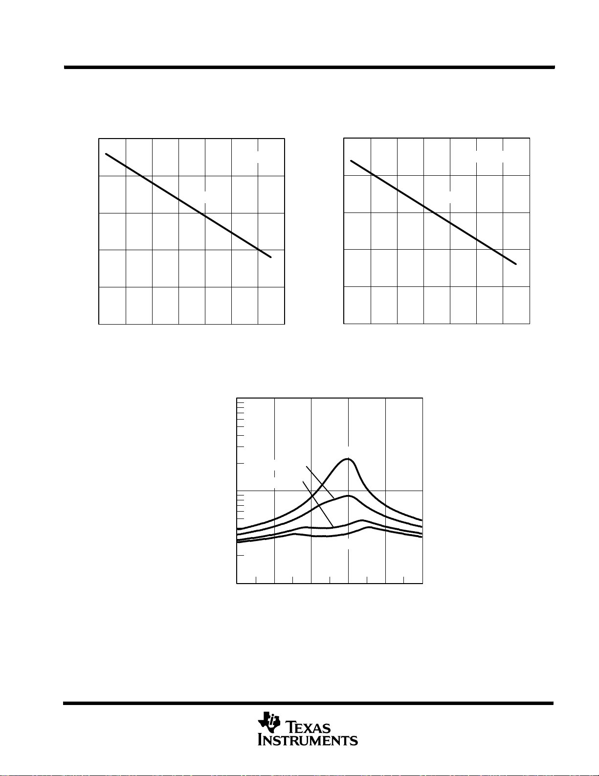
MSP430x241x, MSP430x261x
(
)
(
)
http://www.xinpian.net
提供单片机解密、IC解密、芯片解密业务
010-62245566 13810019655
MIXED SIGNAL MICROCONTROLLER
SLAS541A -- JUNE 2007 -- REVISED OCTOBER 2007
electrical characteristics over recommended ranges of supply voltage and operating free-air
temperature (unless otherwise noted) (continued)
typical characteristics -- Comparator A+
650
VCC=3V
600
Typical
550
500
-- Reference Volts --mV
(REFVT)
450
V
400
-- 4 5 -- 2 5 -- 5 1 5 3 5 5 5 7 5 9 5
TA-- Free-Air Temperature -- °C
Figure 35. V
vs Temperature, VCC=3V
RefVT
100.00
650
VCC=2.2V
600
Typical
550
500
-- Reference Volts --mV
(REFVT)
450
V
400
-- 4 5 -- 2 5 -- 5 1 5 3 5 5 5 7 5 9 5
TA-- Free-Air Temperature -- °C
Figure 36. V
vs Temperature, VCC=2.2V
RefVT
VCC=1.8V
VCC=2.2V
10.00
Short Resistance -- kΩ
1.00
VCC=3.0V
VCC=3.6V
0.0 0.2 0.4 0.6 0.8 1.0
V
Figure 37. Short Resistance vs VIN/V
-- Normalized Input Voltage -- V/V
IN/VCC
CC
POST OFFICE BOX 655303 • DALLAS, TEXAS 75265
61
Page 62

MSP430x241x, MSP430x261x
f
f
ADC12CL
K
=5MHz,ADC12ON=1,REFON=0
A
pgppy
f
(
4)f
ADC12CL
K
=5MHz,ADC12ON=0
http://www.xinpian.net
提供单片机解密、IC解密、芯片解密业务
010-62245566 13810019655
MIXED SIGNAL MICROCONTROLLER
SLAS541A -- JUNE 2007 -- REVISED OCTOBER 2007
electrical characteristics over recommended ranges of supply voltage and operating free-air
temperature (unless otherwise noted) (continued)
12-bit ADC power supply and input range conditions (see Note 1)
PARAMETER TEST CONDITIONS VCC MIN TYP MAX UNIT
AVCCand DVCCare connected together,
AV
AV
CC
V
(P6.x/Ax)
Analog supply voltage
Analog input voltage
(see Note 2)
Operating supply current
I
ADC12
intoAVCCterminal
(see Note 3)
Operating supply current
I
REF+
into AVCCterminal
seeNote
†
C
I
†
R
I
†
Lmits verified by design
Input capacitance
Input MUX ON resistance 0V≤ VAx≤ V
NOTES: 1. The leakage current is defined in the leakage current table with P6.x/Ax parameter.
2. The analog input voltage range must be within the selected reference voltage range V
3. The internal reference supply current is not included in current consumption parameter I
4. The internal reference current is supplied via terminal AV
conversion is active. The REFON bit enables to settle the built-in reference before starting an A/D conversion.
and DVSSare connected together,
SS
V
(AVSS)=V(DVSS)
=0V
All P6.0/A0 to P6.7/A7 terminals.
Analog inputs selected in ADC12MCTLx register
and P6Sel.x = 1, 0 ≤ x ≤ 7,
V
(AVSS)
≤ V
P6.x/Ax
≤ V
(AVCC)
=5MHz,ADC12ON = 1, REFON = 0,
SHT0 = 0, SHT1 = 0, ADC12DIV = 0
f
ADC12CLK
= 5 MHz, ADC12ON = 0,
REFON = 1, REF2_5V = 1
=5MHz,ADC12ON = 0,
,
REFON = 1, REF2_5V = 0
Only one terminal can be selected at one time,
P6.x/Ax
AVC C
. Consumption is independent of the ADC12ON control bit, unless a
CC
2.2 3.6 V
0 V
2.2 V 0.65 0.8
,
3V 0.8 1.0
3V 0.5 0.7
2.2 V 0.5 0.7
3V 0.5 0.7
2.2 V 40 pF
3V 2000 Ω
to V
R+
for valid conversion results.
R--
.
ADC12
AVC C
V
m
mA
12-bit ADC external reference (see Note 1)
PARAMETER TEST CONDITIONS VCC MIN MAX UNIT
V
eREF+
V
REF-- /VeREF--
(V
I
I
-- V
eREF+
VeREF+
VREF--/VeREF--
REF--/VeREF--
NOTES: 1. The external reference is used during conversion to charge and discharge the capacitance array. The input capacitance, Ci,isalso
the dynamic load for an external reference during conversion. The dynamic impedance of the reference supply should follow the
recommendations on analog-source impedance to allow the charge to settle for 12-bit accuracy.
2. The accuracy limits the minimum positive external reference voltage. Lower reference voltage levels may be applied with reduced
accuracy requirements.
3. The accuracy limits the maximum negative external reference voltage. Higher reference voltage levels may be applied with reduced
accuracy requirements.
4. The accuracy limits minimum external differential reference voltage. Lower differential reference voltage levels may be applied with
reduced accuracy requirements.
Positive external
reference voltage input
Negative external
reference voltage input
Differential external
)
reference voltage input
Static input current 0V ≤V
Static input current 0V ≤ V
V
eREF+>VREF--/VeREF--
V
eREF+>VREF--/VeREF--
V
eREF+>VREF--/VeREF--
≤ V
eREF+
eREF--
≤ V
AVC C
AVC C
(see Note 2) 1.4 V
AVC C
(see Note 3) 0 1.2 V
(see Note 4) 1.4 V
AVC C
2.2 V/3 V ±1 μA
2.2 V/3 V ±1 μA
V
V
62
POST OFFICE BOX 655303 • DALLAS, TEXAS 75265
Page 63
MSP430x241x, MSP430x261x
V
)
REF2_5V=1(2.5V)
V
V
)
V
/3V
V
outpu
t
REF2_5V=0(1.5V)
2.2V/3V
A
V
builtinreferenc
e
f
Loadcurrentouto
f
A
A
V
V
http://www.xinpian.net
提供单片机解密、IC解密、芯片解密业务
010-62245566 13810019655
MIXED SIGNAL MICROCONTROLLER
SLAS541A -- JUNE 2007 -- REVISED OCTOBER 2007
electrical characteristics over recommended ranges of supply voltage and operating free-air
temperature (unless otherwise noted) (continued)
12-bit ADC built-in reference
PARAMETER TEST CONDITIONS VCC TA MIN TYP MAX UNIT
-- 4 0 °Cto85°C 2.4 2.5 2.6
105°C 2.37 2.5 2.64
-- 4 0 °Cto85°C 1.44 1.5 1.56
105°C 1.42 1.5 1.57
2.2
2.8
2.9
20 ns
17 ms
V
m
LSB
V
REF+
Positive built-in
reference voltage
REF2_5V = 1(2.5
I
max ≤ I
VREF+
VREF+
REF2_5V = 0(1.5
I
max ≤ I
VREF+
VREF+
≤ I
≤ I
VREF+
VREF+
min
min
3
2.2
2.2 V/3 V
REF2_5V = 0,
I
AV
CC(min)
I
VREF+
I
L(VREF)+
CC
voltage, positive
built-in reference
active
Load current out o
V
REF+
Load-current
†
regulation, V
terminal
minimum
terminal
REF+
max ≤ I
VREF+
REF2_5V = 1,
--0.5mA ≤ I
VREF+
REF2_5V = 1,
-- 1 m A ≤ I
I
VREF+
= 500 μA +/-- 100 μA
VREF+
nalog input voltage ~0.75V,
REF2_5V = 0
I
= 500 μA ± 100 μA
VREF+
Analog input voltage ~1.25 V,
VREF+
≤ I
≤ I
VREF+
≤ I
VREF+
VREF+
min
min
min
2.2 V 0.01 -- 0 . 5
3V 0.01 -- 1
2.2 V ±2
3V ±2
3V ±2
REF2_5V = 1
I
DL(VREF) +
C
VREF+
†
T
REF+
Load current
‡
regulation V
terminal
Capacitance at pin
V
(see Note 1)
REF+
Temperature
coefficient of
built-in reference
REF+
I
= 100 μA → 900 μA,
VREF+
C
VREF+
=5μF, at ~ 0 . 5
REF+
,
Error of conversion result ≤ 1LSB
REFON =1,
0mA≤ I
I
VREF+
of 0 mA ≤ I
≤ I
VREF+
VREF+
max
is a constant in the range
≤ 1mA
VREF+
3
2.2 V/3 V 5 10 μF
2.2 V/3 V ±100 ppm/°C
Settletimeof
t
REFON
internal reference
†
voltage (see
Figure 38 and Note
I
VREF+
V
REF+
=0.5mA,C
=1.5V,V
AVC C
VREF+
=2.2V
=10μF,
2)
†
Limits characterized
‡
Limits verified by design
NOTES: 1. The internal buffer operational amplifier and the accuracy specifications require an external capacitor. All INL and DNL tests use
two capacitors between pins V
2. The condition is that the error in a conversion started after t
and AVSSand V
REF+
REF--/VeREF--
REFON
and AVSS:10μF tantalum and 100 nF ceramic.
is less than ±0.5 LSB. The settling time depends on the external
capacitive load.
POST OFFICE BOX 655303 • DALLAS, TEXAS 75265
63
Page 64

MSP430x241x, MSP430x261x
http://www.xinpian.net
提供单片机解密、IC解密、芯片解密业务
010-62245566 13810019655
MIXED SIGNAL MICROCONTROLLER
SLAS541A -- JUNE 2007 -- REVISED OCTOBER 2007
electrical characteristics over recommended ranges of supply voltage and operating free-air
temperature (unless otherwise noted) (continued)
typical characteristics -- ADC12
C
VREF+
100 μF
t
10 μF
1 μF
REFON
≈ .66xC
VREF+
[ms] with C
VREF+
in μF
0
1ms
10 ms
Figure 38. Typical Settling Time of Internal Reference t
100 ms t
REFON
REFON
vs External Capacitor on V
REF
+
64
POST OFFICE BOX 655303 • DALLAS, TEXAS 75265
Page 65
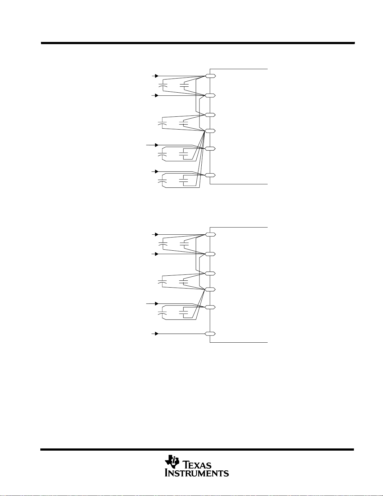
MSP430x241x, MSP430x261x
http://www.xinpian.net
提供单片机解密、IC解密、芯片解密业务
010-62245566 13810019655
MIXED SIGNAL MICROCONTROLLER
SLAS541A -- JUNE 2007 -- REVISED OCTOBER 2007
electrical characteristics over recommended ranges of supply voltage and operating free-air
temperature (unless otherwise noted) (continued)
From
Apply External Reference [V
or Use Internal Reference [V
Power
Supply
eREF+
]
REF+
Apply
External
Reference
]
+
--
10 μ F 100 nF
+
--
10 μ F 100 nF
+
--
10 μ F 100 nF
+
--
10 μ F 100 nF
Figure 39. Supply Voltage and Reference Voltage Design V
From
Power
Supply
+
--
10 μ F 100 nF
DV
DV
AV
AV
V
V
DV
DV
CC
SS
CC
SS
REF+
REF
CC
SS
or V
-- / V
MSP430F261x
MSP430F241x
eREF+
eREF--
REF--/VeREF--
External Supply
+
--
Apply External Reference [V
or Use Internal Reference [V
Reference Is Internally
Switched to AV
eREF+
REF+
]
]
SS
10 μ F 100 nF
+
--
10 μ F 100 nF
Figure 40. Supply Voltage and Reference Voltage Design V
AV
CC
MSP430F261x
AV
MSP430F241x
SS
or V
V
REF+
V
REF--/VeREF--
REF--/VeREF--
eREF+
=AVSS, Internally Connected
POST OFFICE BOX 655303 • DALLAS, TEXAS 75265
65
Page 66

MSP430x241x, MSP430x261x
‡
RS=40
0
Ω
RI=1000
Ω
CI=30pF
V
/3V
http://www.xinpian.net
提供单片机解密、IC解密、芯片解密业务
010-62245566 13810019655
MIXED SIGNAL MICROCONTROLLER
SLAS541A -- JUNE 2007 -- REVISED OCTOBER 2007
electrical characteristics over recommended ranges of supply voltage and operating free-air
temperature (unless otherwise noted) (continued)
12-bit ADC timing parameters
PARAMETER TEST CONDITIONS VCC MIN TYP MAX UNIT
f
ADC12CLK
f
ADC12OSC
t
CONVERT
t
ADC12ON
t
Sample
†
Limits characterized
‡
Limits verified by design
Internal ADC12 oscillator
Conversion time
Turn-onsettlingtimeof
‡
the ADC
Sampling time
NOTES: 1. The condition is that the error in a conversion started after t
settled.
2. Approximately ten Tau (τ) are needed to get an error of less than ±0.5 LSB:
t
Sample
=ln(2
n+1
)x(RS+RI)xCI+ 800 ns where n = ADC resolution = 12, RS= external source resistance.
12-bit ADC linearity parameters
PARAMETER TEST CONDITIONS VCC MIN TYP MAX UNIT
EIIntegral linearity error
EDDifferential linearity error
E
Offset error
O
E
Gain error
G
E
Total unadjusted error
T
For specified performance of ADC12
linearity parameters
ADC12DIV = 0,
f
ADC12CLK=fADC12OSC
C
≥ 5 μF, Internal oscillator,
VREF+
f
ADC12OSC
External f
= 3.7 MHz to 6.3 MHz
ADC12CLK
from ACLK, MCLK
or SMCLK, ADC12SSEL ≠ 0
2.2V/3 V 0.45 5 6.3 MHz
2.2 V/ 3 V 3.7 5 6.3 MHz
2.2 V/ 3 V 2.06 3.51
13 × ADC12DIV
× 1/f
ADC12CLK
SeeNote1 100 ns
R
= 400 Ω,R
τ =[R
S+RI
1.4 V ≤ (V
1.6 V < (V
(V
C
(V
eREF+
eREF+
-- V
eREF+
VREF+
eREF+
REF--/VeREF--)min
=10μF (tantalum) and 100 nF (ceramic)
-- V
REF--/VeREF--)min
= 1000 Ω,C
,
]xCI;(see Note 2)
-- V
REF--/VeREF--
-- V
REF--/VeREF--
≤ (V
≤ (V
Internal impedance of source R
C
=10μF (tantalum) and 100 nF (ceramic)
VREF+
(V
C
(V
C
-- V
eREF+
VREF+
eREF+
VREF+
REF--/VeREF--)min
=10μF (tantalum) and 100 nF (ceramic)
-- V
REF--/VeREF--)min
=10μF (tantalum) and 100 nF (ceramic)
≤ (V
≤ (V
=30pF,
,
ADC12ON
)min≤ 1.6 V
)min≤ V
S
eREF+
eREF+
< 100 Ω,
eREF+
eREF+
AVC C
-- V
-- V
-- V
-- V
,
is less than ±0.5 LSB. The reference and input signal are already
REF--/VeREF--
REF--/VeREF--
REF--/VeREF--
REF--/VeREF--
3V 1220
2.2 V 1400
2.2
),
2.2 V/3 V ±1 LSB
),
2.2 V/3 V ±2 ±4 LSB
),
2.2 V/3 V ±1.1 ±2 LSB
),
2.2 V/3 V ±2 ±5 LSB
±2
±1.7
μs
ns
LSB
66
POST OFFICE BOX 655303 • DALLAS, TEXAS 75265
Page 67

MSP430x241x, MSP430x261x
p
ply
Operatingsupplycurrentint
o
REFON=0,INCH=0A
h
A
A
ADC12ON=1,INCH=0A
h
V
A
V
/
Sampletimerequiredifchannel
ADC12ON=1,INCH=0A
h
Currentintodivideratchannel11
A
A
A
A
ADC12ON=1,INCH=0B
h
V
Sampletimerequiredifchannel
ADC12ON=1,INCH=0B
h
http://www.xinpian.net
提供单片机解密、IC解密、芯片解密业务
010-62245566 13810019655
MIXED SIGNAL MICROCONTROLLER
SLAS541A -- JUNE 2007 -- REVISED OCTOBER 2007
electrical characteristics over recommended operating free-air temperature (unless otherwise
noted) (continued)
12-bit ADC temperature sensor and built-in V
PARAMETER
I
SENSOR
SENSOR
SENSOR
MID
†
†
V
TC
t
SENSOR(sample)
I
VMID
V
t
VMID(sample)
†
Limits characterized
Operatingsu
AVCCterminal (see Note 1)
SeeNote2
Sample time required ifchannelADC12ON = 1, INCH = 0Ah,
†
10 is selected (see Note 3)
Current into divider at channel 11
(see Note 4)
VCCdivider at channel 11
Sample time required ifchannelADC12ON = 1, INCH = 0Bh,
11 is selected (see Note 5)
NOTES: 1. The sensor current I
is high). W hen REFON = 1, I
2. The temperature sensor offset can be as much as ±20_C. A single-point calibration is recommended in order to minimize the offset
error of the built-in temperature sensor.
3. The typical equivalent impedance of the sensor is 51 k Ω. The sample time required includes the sensor-on time t
4. No additional current is needed. The V
5. Theontimet
VMID(on)
current into REFON = 0, INCH = 0Ah,
ADC12ON = 1, T
T
A
Error of conversion result ≤ 1LSB
V
Error of conversion result ≤ 1LSB
is consumed if (ADC12ON = 1 and REFON = 1) or if (ADC12ON = 1, INCH = 0Ah and sample signal
SENSOR
is already included in I
SENSOR
MID
is used during sampling.
is included in the sampling time t
MID
TEST CONDITIONS VCC MIN TYP MAX UNIT
,
=25_C
A
DC12ON = 1, INCH = 0Ah,
=0°C
DC12ON = 1, INCH = 0Ah
,
,
2.2 V 40 120
3V 60 160
2.2 V 986
3V 986
2.2 V 3.55
3V 3.55
2.2 V 30
3V 30
DC12ON = 1, INCH = 0Bh
DC12ON = 1, INCH = 0Bh,
is ~0.5 x V
MID
AVC C
,
,
2.2 V NA
3V NA
2.2 V 1.1 1.1±0.04
3V 1.5 1.50±0.04
2.2 V 1400
3V 1220
.
REF+
VMID(sample)
; no additional on time is needed.
m
m
SENSOR(on)
μ
°C
μs
μ
ns
.
POST OFFICE BOX 655303 • DALLAS, TEXAS 75265
67
Page 68
MSP430x241x, MSP430x261x
DAC12AMPx2,DAC12IR0
,
V
/3V
Supplycurrent,singl
e
http://www.xinpian.net
提供单片机解密、IC解密、芯片解密业务
010-62245566 13810019655
MIXED SIGNAL MICROCONTROLLER
SLAS541A -- JUNE 2007 -- REVISED OCTOBER 2007
electrical characteristics over recommended ranges of supply voltage and operating free-air
temperature (unless otherwise noted) (continued)
12-bit DAC supply specifications
PARAMETER TEST CONDITIONS VCC T
AV
Analog supply voltage
CC
AVCC=DVCC,
AV
=DVSS=0V
SS
DAC12AMPx = 2, DAC12IR = 0,
DAC12_xDAT = 0x0800
2.2
A
-- 4 0 °Cto85°C 50 110
105°C 69 150
DAC12AMPx = 2, DAC12IR = 1,
DAC12_xDAT = x00800
Supply current, single
I
DD
DAC channel
(see Notes 1 and 2)
V
eREF+=VREF+
DAC12AMPx = 5, DAC12IR = 1,
DAC12_xDAT = 0x0800,
V
eREF+=VREF+
=AV
=AV
,
CC
CC
2.2V/3V 50 130
2.2V/3V 200 440
DAC12AMPx = 7, DAC12IR = 1,
PSRR
Power-supply rejection
ratio
(see Notes 3 and 4)
DAC12_xDAT = 0x0800,
V
eREF+=VREF+
=AV
CC
DAC12_xDAT = 800h, V
∆AV
= 100mV
CC
DAC12_xDAT = 800h, V
∆AV
= 100mV
CC
=1.5V,
REF
= 1.5 V or 2.5 V,
REF
2.2V/3V 700 1500
2.2V
3V
NOTES: 1. No load at the output pin, DAC12_0 or DAC12_1, assuming that the control bits for the shared pins are set properly.
2. Current into reference terminals not included. If DAC12IR = 1 current flows through the input divider; see Reference Input
specifications.
3. PSRR = 20 × log{∆AV
4. V
is applied externally. The internal reference is not used.
REF
CC
/∆V
DAC12_xOUT
}
MIN TYP MAX UNIT
2.20 3.60 V
μA
70 dB
68
POST OFFICE BOX 655303 • DALLAS, TEXAS 75265
Page 69

MSP430x241x, MSP430x261x
f
f
y
Differentialnonlinearit
y
f
f
Offsetvoltagewithoutcalibration
E
O
f
f
VOffsetvoltagewithcalibration
t
Offset_Ca
l
(
3
)
2.2V/3V6m
s
http://www.xinpian.net
提供单片机解密、IC解密、芯片解密业务
010-62245566 13810019655
MIXED SIGNAL MICROCONTROLLER
SLAS541A -- JUNE 2007 -- REVISED OCTOBER 2007
electrical characteristics over recommended operating free-air temperature (unless otherwise
noted) (continued)
12-bit DAC linearity specifications (see Figure 41)
PARAMETER TEST CONDITIONS VCC MIN TYP MAX UNIT
Resolution 12-bit monotonic 12 bits
V
=1.5V
REF
DAC12AMPx = 7, DAC12IR = 1
INL Integral nonlinearity (see Note 1)
V
=2.5V
REF
DAC12AMPx = 7, DAC12IR = 1
V
=1.5V
REF
DNL
Di
erential nonlinearit
(see Note 1)
DAC12AMPx = 7, DAC12IR = 1
V
=2.5V
REF
DAC12AMPx = 7, DAC12IR = 1
V
=1.5V
REF
O
set voltage without calibration
(see Notes 1 and 2)
E
O
set voltage with calibration
(see Notes 1 and 2)
DAC12AMPx = 7, DAC12IR = 1
V
=2.5V
REF
DAC12AMPx = 7, DAC12IR = 1
V
=1.5V
REF
DAC12AMPx = 7, DAC12IR = 1
V
=2.5V
REF
DAC12AMPx = 7, DAC12IR = 1
d
E(O)/dT
E
G
d
E(G)/dT
Offset error temperature
coefficient (see Note 1)
Gainerror(seeNote1)
Gain temperature
coefficient (see Note 1)
V
=1.5V 2.2 V
REF
V
=2.5V 3V
REF
DAC12AMPx = 2 100
t
Offset Cal
Time for offset calibration
seeNote
DAC12AMPx = 3, 5
DAC12AMPx = 4, 6, 7
NOTES: 1. Parameters calculated from the best-fit curve from 0x0A to 0xFFF. The best-fit curve method is used to deliver coefficients “a” and
“b” of the first order equation: y = a + b × x. V
DAC12_xOUT=EO
+(1+EG) × (V
2. The offset calibration works on the output operational amplifier. Offset calibration is triggered setting bit DAC12CALON.
3. The offset calibration can be done if DAC12AMPx = {2, 3, 4, 5, 6, 7}. The output operational amplifier is switched off with
DAC12AMPx = {0, 1}. It is recommended that the DAC12 module be configured prior to initiating calibration. Port activity during
calibration may affect accuracy and is not recommended.
2.2 V
±2.0 ±8.0 LSB
3V
2.2 V
±0.4 ±1.0 LSB
3V
2.2 V
±21
3V
2.2 V
±2.5
3V
2.2 V/3 V 30 μV/C
±3.50 % FSR
2.2 V/3 V 10
2.2 V/3 V
/4095) × DAC12_xDAT, DAC12IR = 1.
eREF+
ppm of
FSR/°C
32
m
ms
DAC Output
Figure 41. Linearity Test Load Conditions and Gain/Offset Definition
C
R
Load
Load
=
AV
CC
2
= 100pF
POST OFFICE BOX 655303 • DALLAS, TEXAS 75265
DAC V
OUT
V
R+
Offset Error
Positive
Negative
Ideal transfer
function
Gain Error
DAC Code
69
Page 70

MSP430x241x, MSP430x261x
http://www.xinpian.net
提供单片机解密、IC解密、芯片解密业务
010-62245566 13810019655
MIXED SIGNAL MICROCONTROLLER
SLAS541A -- JUNE 2007 -- REVISED OCTOBER 2007
electrical characteristics over recommended operating free-air temperature (unless otherwise
noted) (continued)
typical characteristics -- 12-bit DAC, linearity specifications
TYPICAL INL ERROR
vs
DIGITAL INPUT DATA
4
VCC=2.2V,V
DAC12AMPx = 7
3
DAC12IR = 1
2
1
0
-- 1
REF
=1.5V
-- 2
INL -- Integral Nonlinearity Error -- LSB
-- 3
-- 4
0 512 1024 1536 2048 2560 3072 3584
DAC12_xDAT -- Digital Code
TYPICAL DNL ERROR
vs
DIGITAL INPUT DATA
2.0
1.5
1.0
0.5
0.0
-- 0 . 5
-- 1 . 0
VCC=2.2V,V
DAC12AMPx = 7
DAC12IR = 1
REF
=1.5V
4095
-- 1 . 5
DNL -- Differential Nonlinearity Error -- LSB
-- 2 . 0
0 512 1024 1536 2048 2560 3072 3584
70
4095
DAC12_xDAT -- Digital Code
POST OFFICE BOX 655303 • DALLAS, TEXAS 75265
Page 71
MSP430x241x, MSP430x261x
Outputvoltagerang
e
V
/3V
V
A
(seeFigure44)
http://www.xinpian.net
提供单片机解密、IC解密、芯片解密业务
010-62245566 13810019655
MIXED SIGNAL MICROCONTROLLER
SLAS541A -- JUNE 2007 -- REVISED OCTOBER 2007
electrical characteristics over recommended operating free-air temperature (unless otherwise
noted) (continued)
12-bit DAC output specifications
PARAMETER TEST CONDITIONS VCC MIN TYP MAX UNIT
No Load, Ve
DAC12_xDAT = 0h, DAC12IR = 1,
DAC12AMPx = 7
No Load, Ve
DAC12_xDAT = 0FFFh,
V
O
Output voltagerange
(see Note 1 and Figure 44)
DAC12IR = 1, DAC12AMPx = 7
R
=3kΩ,Ve
Load
DAC12_xDAT = 0h, DAC12IR = 1,
DAC12AMPx = 7
R
=3kΩ,Ve
Load
DAC12_xDAT = 0FFFh, DAC12IR =
1, DAC12AMPx = 7
C
L(DAC12)
I
L(DAC12)
Max DAC12 load
capacitance
Max DAC12 load current
R
Load
=3kΩ,V
DAC12AMPx = 7, DAC12_xDAT = 0h
R
=3kΩ,V
Load
R
O/P(DAC12)
Output resistance
(see Figure 44)
DAC12AMPx = 7,
DAC12_xDAT = 0FFFh
R
=3kΩ,
Load
0.3 V <
V
DAC12AMPx = 7
NOTE 1: Data is valid after the offset calibration of the output amplifier.
R
I
Load
Load
DAC12
C
O/P(DAC12_x)
Load
= 100pF
Figure 44. DAC12_x Output Resistance Tests
REF+
REF+
REF+
REF+
O/P(DAC12)
O/P(DAC12)
O/P(DAC12)
AV
CC
2
=AVCC,
=AVCC,
=AVCC,
=AVCC,
=0V,
=AVCC,
< AVCC-- 0 . 3 V ,
2.2
2.2 V/3 V 100 pF
2.2 V/3 V
R
O/P(DAC12_x)
0 0.005
AVCC--0.05 AV
CC
0 0.1
AVCC--0.13 AV
CC
2.2V -- 0 . 5 +0.5
3V -- 1 . 0 +1.0
150 250
150 250
1 4
Max
Min
0.3
AVCC--0.3V
AV
CC
m
Ω
V
OUT
POST OFFICE BOX 655303 • DALLAS, TEXAS 75265
71
Page 72

MSP430x241x, MSP430x261x
Referenceinputvoltage
V
/3V
V
(VREF+)
p
2.2V/3V
_
,
O
N
(
d
/
μ
)
t
S(FS)
ful
l
80h→F7F
h→80h
2.2V/3V
μ
s
)
DAC12_xDA
T
t
S(C-C
)
3F8h408h3F8
h
2.2V/3V
μ
s
SRSlewrate80h→F7F
h→80h
2.2V/3V
V
/μs
ful
l
80h→F7F
h→80h
2.2V/3V30nVs
http://www.xinpian.net
提供单片机解密、IC解密、芯片解密业务
010-62245566 13810019655
MIXED SIGNAL MICROCONTROLLER
SLAS541A -- JUNE 2007 -- REVISED OCTOBER 2007
electrical characteristics over recommended operating free-air temperature (unless otherwise
noted) (continued)
12-bit DAC reference input specifications
PARAMETER TEST CONDITIONS VCC MIN TYP MAX UNIT
Ve
REF+
Reference input voltage
range
DAC12IR = 0, (see Notes 1 and 2)
DAC12IR = 1, (see Notes 3 and 4)
2.2
DAC12_0 IR = DAC12_1 IR = 0 20 MΩ
DAC12_0 IR = 1, DAC12_1 IR = 0
Ri
Ri
(VREF+)
(VeREF+)
,
Reference input
resistance
DAC12_0 IR = 0, DAC12_1 IR = 1
DAC12_0 IR = DAC12_1 IR = 1
DAC12_0 SREFx = DAC12_1 SREFx
(see Note 5)
NOTES: 1. For a full-scale output, the reference input voltage can be as high as 1/3 of the maximum output voltage swing (AVCC).
2. The maximum voltage applied at reference input voltage terminal Ve
REF+
=[AVCC-- V
E(O)
3. For a full-scale output, the reference input voltage can be as high as the maximum output voltage swing (AV
4. The maximum voltage applied at reference input voltage terminal Ve
REF+
=[AVCC-- V
E(O)
5. When DAC12IR = 1 and DAC12SREFx = 0 or 1 for both channels, the reference input resistive dividers for each DAC are in parallel
reducing the reference input resistance.
AVCC/3 AVCC+0.2
AVc c AVcc+0.2
40 48 56
20 24 28
]/[3*(1+EG)].
).
CC
]/(1+EG).
kΩ
12-bit DAC dynamic specifications, V
ref=VCC
, DAC12IR = 1 (see Figure 45 and Figure 46)
PARAMETER TEST CONDITIONS VCC MIN TYP MAX UNIT
DAC12_xDAT = 800h,
t
ON
DAC12 on-time
Error
< ±0.5 LSB
V(O)
seeNote1an
Figure 45)
DAC12AMPx = 0 → {2,3,4} 60 120
DAC12AMPx = 0 → {5, 6}
DAC12AMPx = 0 → 7
2.2 V/3 V
15 30
6 12
DAC12AMPx = 2 100 200
t
S(FS
t
S(C-C
Settling time,
scale
Settling time,
codetocode
DAC12_xDAT =
=
=
3F8h→ 408h→ 3F8h
BF8h→ C08h→ BF8h
DAC12AMPx = 3, 5
DAC12AMPx = 4, 6, 7
2.2 V/3 V
40 80
15 30
DAC12AMPx = 2 5
DAC12AMPx = 3, 5
2.2 V/3 V
DAC12AMPx = 4, 6, 7
2
1
DAC12AMPx = 2 0.05 0.12
SR Slew rate
DAC12_xDAT =
DAC12AMPx = 3, 5
DAC12AMPx = 4, 6, 7
2.2 V/3 V
0.35 0.7
1.5 2.7
DAC12AMPx = 2 600
Glitch energy,
scale
DAC12_xDAT =
DAC12AMPx = 3, 5
2.2 V/3 V
150
DAC12AMPx = 4, 6, 7
NOTES: 1. R
Load
and C
are connected to AVSS(not AVCC/2) in Figure 45.
Load
2. Slew rate applies to output voltage steps ≥ 200 mV.
DAC Output
R
O/P(DAC12.x)
I
Load
R
C
Load
Load
=3kΩ
= 100pF
AV
Conversion 1 Conversion 2
V
OUT
Glitch
+/-- 1/2 LSB
Energy
CC
2
Conversion 3
+/-- 1/2 LSB
μs
μs
μs
V/μs
nV-s
72
t
settleLH
Figure 45. Settling Time and Glitch Energy Testing
POST OFFICE BOX 655303 • DALLAS, TEXAS 75265
t
settleHL
Page 73

MSP430x241x, MSP430x261x
(
F
i
47)
Channeltochannelcrosstalk
V
/
http://www.xinpian.net
提供单片机解密、IC解密、芯片解密业务
010-62245566 13810019655
MIXED SIGNAL MICROCONTROLLER
SLAS541A -- JUNE 2007 -- REVISED OCTOBER 2007
electrical characteristics over recommended ranges of supply voltage and operating free-air
temperature (unless otherwise noted) (continued)
Conversion 1 Conversion 2
V
OUT
90%
10%
t
SRLH
Figure 46. Slew Rate Testing
12-bit DAC, dynamic specifications (continued) (T
PARAMETER TEST CONDITIONS VCC MIN TYP MAX UNIT
DAC12AMPx = {2, 3, 4}, DAC12SREFx = 2,
DAC12IR = 1, DAC12_xDAT = 800h
BW
--3dB
NOTE 1: R
3-dB bandwidth,
V
=1.5V, VAC=0.1V
DC
see
gure
Channel-to-channel crosstalk
(see Note 1 and Figure 48)
LOAD
=3kΩ,C
LOAD
= 100 pF
AC
DC
DAC12AMPx = {5, 6}, DAC12SREFx = 2,
PP
DAC12IR = 1, DAC12_xDAT = 800h
DAC12AMPx = 7, DAC12SREFx = 2,
DAC12IR = 1, DAC12_xDAT = 800h
DAC12_0DAT = 800h, No load,
DAC12_1DAT = 80h<-->F7Fh, R
f
DAC12_1OUT
DAC12_0DAT = 80h<-->F7Fh, R
DAC12_1DAT = 800h, No load,
f
DAC12_0OUT
Ve
REF+
= 10 kHz, Duty cycle = 50%
= 10 kHz, Duty cycle = 50%
DAC12_x
Conversion 3
90%
10%
t
SRHL
=25°C, unless otherwise noted)
A
2.2 V/3 V
=3kΩ,
Load
2.2
I
Load
DACx
Load
C
=3kΩ,
R
Load
Load
=3kΩ
= 100pF
AV
3V
CC
2
40
180
550
kHz
-- 8 0
dB
-- 8 0
DAC12_0
V
REF+
DAC12_1
Figure 47. Test Conditions for 3-dB Bandwidth Specification
R
C
C
Load
Load
Load
= 100pF
R
Load
= 100pF
AV
AV
CC
2
CC
2
DAC12_xDAT 080h
V
OUT
V
DAC12_yOUT
V
DAC12_xOUT
7F7h
f
Toggle
I
Load
DAC0
I
Load
DAC1
Figure 48. Crosstalk Test Conditions
POST OFFICE BOX 655303 • DALLAS, TEXAS 75265
080h 7F7h 080h
73
Page 74

MSP430x241x, MSP430x261x
http://www.xinpian.net
提供单片机解密、IC解密、芯片解密业务
010-62245566 13810019655
MIXED SIGNAL MICROCONTROLLER
SLAS541A -- JUNE 2007 -- REVISED OCTOBER 2007
electrical characteristics over recommended ranges of supply voltage and operating free-air
temperature (unless otherwise noted) (continued)
flash memory
PARAMETER
V
CC(PGM/ERASE)
f
FTG
I
PGM
I
ERASE
t
CPT
t
CMErase
Program and erase supply voltage 2.2 3.6 V
Flash Timing Generator frequency 257 476 kHz
Supply current from DVCCduring program 2.2 V/ 3.6 V 3 5 mA
Supply current from DVCCduring erase 2.2 V/ 3.6 V 3 7 mA
Cumulative program time SeeNote1 2.2 V/ 3.6 V 4 ms
Cumulative mass erase time SeeNote2 2.2 V/ 3.6 V 200 ms
Program/Erase endurance 10
t
Retention
t
Word
t
Block, 0
t
Block, 1-63
t
Block, End
t
Mass Erase
t
Seg Erase
Data retention duration TJ=25°C 100 years
Word or byte program time SeeNote3 35 t
Block program time for first byte or word SeeNote3 30 t
Block program time for each additional byte or word SeeNote3 21 t
Block program end-sequence wait time SeeNote3 6 t
Masserasetime(seeNote4) SeeNote3 10593 t
Segment erase time SeeNote3 4819 t
NOTES: 1. The cumulative program time must not be exceeded when writing to a 64-byte flash block. This parameter applies to all programming
methods: individual word/byte write and block write modes.
2. The mass erase duration generated by the flash timing generator is at least 11.1 ms ( = 5297x1/f
achieve the required cumulative mass erase time, the Flash Controller’s mass erase operation can be repeated until this time is met.
A worst case minimum of 19 cycles is required.
3. These values are hardwired into the Flash Controller’s state machine (t
4. To erase the complete code area, the mass erase must be performed once with a dummy address in the range of the lower 64-kB
flash addresses and once with the dummy address in the upper 64-kB flash addresses.
TEST
CONDITIONS
FTG
VCC MIN TYP MAX UNIT
=1/f
FTG
4
FTG
).
5
10
,max = 5297 × 1/476 kHz). To
cycles
FTG
FTG
FTG
FTG
FTG
FTG
RAM
PARAMETER TEST CONDITIONS MIN MAX UNIT
VRAMh SeeNote1 CPU halted 1.6 V
NOTE 1: This parameter defines the minimum supply voltage when the data in program memory RAM remain unchanged. No program execution
should take place during this supply voltage condition.
74
POST OFFICE BOX 655303 • DALLAS, TEXAS 75265
Page 75

MSP430x241x, MSP430x261x
f
http://www.xinpian.net
提供单片机解密、IC解密、芯片解密业务
010-62245566 13810019655
MIXED SIGNAL MICROCONTROLLER
SLAS541A -- JUNE 2007 -- REVISED OCTOBER 2007
electrical characteristics over recommended operating free-air temperature (unless otherwise
noted) (continued)
JTAG interface
PARAMETER
TCK
R
Internal
NOTES: 1. f
TCK inputfrequency See Note 1
Internal pullup resistance on TMS, TCK, TDI/TCLK SeeNote2 2.2 V/ 3 V 25 60 90 kΩ
may be restricted to meet the timing requirements of the module selected.
TCK
2. TMS, TDI/TCLK, and TCK pullup resistors are implemented in all versions.
JTAG fuse (see Note 1)
PARAMETER TEST CONDITIONS MIN MAX UNIT
V
CC(FB)
V
FB
I
FB
t
FB
NOTE 1: Once the fuse is blown, no further access to the MSP430 JTAG/Test and emulation features is possible. The JTAG block is switched
Supply voltage during fuse-blow condition TA=25°C 2.5 V
Voltage level on TDI/TCLK for fuse blow (F versions) 6 7 V
Supply current into TDI/TCLK during fuse blow 100 mA
Time to blow fuse 1 ms
to bypass mode.
TEST
CONDITIONS
V
CC
2.2 V 0 5
3V 0 10
MIN TYP MAX UNIT
MHz
POST OFFICE BOX 655303 • DALLAS, TEXAS 75265
75
Page 76

MSP430x241x, MSP430x261x
http://www.xinpian.net
提供单片机解密、IC解密、芯片解密业务
010-62245566 13810019655
MIXED SIGNAL MICROCONTROLLER
SLAS541A -- JUNE 2007 -- REVISED OCTOBER 2007
APPLICATION INFORMATION
Port P1 pin schematic: P1.0 to P1.7, input/output with Schmitt trigger
P1REN.x
P1DIR.x
P1OUT.x
Module X OUT
P1SEL.x
P1IN.x
Module X IN
P1IRQ.x
0
1
0
1
P1SEL.x
P1IES.x
EN
D
P1IE.x
P1IFG.x
Direction
0: Input
1: Output
EN
Q
Set
Interrupt
Edge Select
DVSS
DVCC
Pad Logic
0
1
1
P1.0/TACLK/CAOUT
P1.1/TA0
P1.2/TA1
P1.3/TA2
P1.4/SMCLK
P1.5/TA0
P1.6/TA1
P1.7/TA2
76
POST OFFICE BOX 655303 • DALLAS, TEXAS 75265
Page 77

Port P1 (P1.0 to P1.7) pin functions
X
/
/
/
/
/
/
/
/
http://www.xinpian.net
提供单片机解密、IC解密、芯片解密业务
010-62245566 13810019655
PIN NAME (P1.X)
P1.0/TACLK 0
P1.1/TA0 1
P1.2/TA1 2
P1.3/TA2 3
P1.4/SMCLK 4
P1.5/TA0 5
P1.6/TA1 6
P1.7/TA2 7
P1.0 (I/O) I: 0; O: 1 0
Timer_A3.TACLK 0 1
CAOUT 1 1
P1.1 (I/O) I: 0; O: 1 0
Timer_A3.CCI0A 0 1
Timer_A3.TA0 1 1
P1.2 (I/O) I: 0; O: 1 0
Timer_A3.CCI0A 0 1
Timer_A3.TA0 1 1
P1.3 (I/O) I: 0; O: 1 0
Timer_A3.CCI0A 0 1
Timer_A3.TA0 1 1
P1.4 (I/O) I: 0; O: 1 0
SMCLK 1 1
P1.5 (I/O) I: 0; O: 1 0
Timer_A3.CCI0A 0 1
Timer_A3.TA0 1 1
P1.6 (I/O) I: 0; O: 1 0
Timer_A3.CCI0A 0 1
Timer_A3.TA1 1 1
P1.7 (I/O) I: 0; O: 1 0
Timer_A3.CCI0A 0 1
Timer_A3.TA2 1 1
FUNCTION
MSP430x241x, MSP430x261x
MIXED SIGNAL MICROCONTROLLER
SLAS541A -- JUNE 2007 -- REVISED OCTOBER 2007
CONTROL BITS / SIGNALS
P1DIR.x P1SEL.x
POST OFFICE BOX 655303 • DALLAS, TEXAS 75265
77
Page 78

MSP430x241x, MSP430x261x
http://www.xinpian.net
提供单片机解密、IC解密、芯片解密业务
010-62245566 13810019655
MIXED SIGNAL MICROCONTROLLER
SLAS541A -- JUNE 2007 -- REVISED OCTOBER 2007
Port P2 pin schematic: P2.0 to P2.4, P2.6, and P2.7, input/output with Schmitt trigger
Pad Logic
Comparator_A
To
Comparator_A
From
CAPD.x
P2REN.x
P2DIR.x
P2OUT.x
Module X OUT
P2SEL.x
P2IN.x
Module X IN
P2IRQ.x
DVSS
0
1
0
1
EN
D
P2IE.x
P2IFG.x
Direction
0: Input
1: Output
EN
Q
Set
DVCC
Bus
Keeper
EN
0
1
1
P2.0/ACLK/CA2
P2.1/TAINCLK/CA3
P2.2/CAOUT/TA0/CA4
P2.3/CA0/TA1
P2.4/CA1/TA2
P2.6/ADC12CLK/
DMAE0/CA6
P2.7/TA0/CA7
P2SEL.x
P2IES.x
78
Interrupt
Edge Select
POST OFFICE BOX 655303 • DALLAS, TEXAS 75265
Page 79
Port P2.0, P2.3, P2.4, P2.6 and P2.7 pin functions
X
/
/
/
/
///
/
/
/
/
/
/
/
/
http://www.xinpian.net
提供单片机解密、IC解密、芯片解密业务
010-62245566 13810019655
PIN NAME (P2.X)
P2.0/ACLK/CA2 0
P2.1/TAINCLK/CA3 1
P2.2/CAOUT/TA0/ 2
CA4
P2.3/CA0/TA1 3
P2.4/CA1/TA2 4
P2.6/ADC12CLK/ 6
DMAE0/CA6
P2.7/TA0/CA7 7
NOTE: X: Don’t care
P2.0 (I/O) 0 I: 0; O: 1 0
ACLK 0 1 1
CA2 1 X X
P2.1 (I/O) 0 I: 0; O: 1 0
Timer_A3.INCLK 0 0 1
DV
SS
CA3 1 X X
P2.2 (I/O) 0 I: 0; O: 1 0
CAOUT 0 1 1
TA0 0 0 1
CA4 1 X X
P2.3 (I/O) 0 I: 0; O: 1 0
Timer_A3.TA1 0 1 1
CA0 1 X X
P2.4 (I/O) 0 I: 0; O: 1 0
Timer_A3.TA2 0 1 X
CA1 1 X 1
P2.6 (I/O) 0 I: 0; O: 1 0
ADC12CLK 0 1 1
DMAE0 0 0 1
CA6 1 X X
P2.7 (I/O) 0 I: 0; O: 1 0
Timer_A3.TA0 0 1 1
CA7 1 X X
FUNCTION
MSP430x241x, MSP430x261x
MIXED SIGNAL MICROCONTROLLER
SLAS541A -- JUNE 2007 -- REVISED OCTOBER 2007
CONTROL BITS / SIGNALS
CAPD.x P2DIR.x P2SEL.x
0 1 1
POST OFFICE BOX 655303 • DALLAS, TEXAS 75265
79
Page 80

MSP430x241x, MSP430x261x
X
/
OSC
/
http://www.xinpian.net
提供单片机解密、IC解密、芯片解密业务
010-62245566 13810019655
MIXED SIGNAL MICROCONTROLLER
SLAS541A -- JUNE 2007 -- REVISED OCTOBER 2007
Port P2 pin schematic: P2.5, input/output with Schmitt trigger
To Comparator
From Comparator
CAPD.5
To DCO
DCOR
P2REN.5
P2DIR.5
P2OUT.5
Module X OUT
P2SEL.x
P2IN.5
in DCO
0
1
0
1
EN
Direction
0: Input
1: Output
DVSS
DVCC
Bus
Keeper
EN
Pad Logic
0
1
1
P2.5/ROSC/CA5
Module X IN
P2IRQ.5
Port P2.5 pin functions
PIN NAME (P2.X)
P2.5/R
NOTES: 1. X: Don’t care
/CA5 5
OSC
2. If Rosc is used it is connected to an external resistor.
D
P2IE.5
P2IFG.5
P2SEL.5
P2IES.5
FUNCTION
P2.5 (I/O) 0 0 I: 0; O: 1 0
R
(see Note 2) 0 1 X X
OSC
DV
SS
CA5 1 or selected 0 X X
EN
Q
Set
Interrupt
Edge Select
CONTROL BITS / SIGNALS
CAPD DCOR P2DIR.5 P2SEL.5
0 0 1 1
80
POST OFFICE BOX 655303 • DALLAS, TEXAS 75265
Page 81

MIXED SIGNAL MICROCONTROLLER
X
/
/
/
/
/
/
/
/
/
/
/
/
/
/
/
/
http://www.xinpian.net
提供单片机解密、IC解密、芯片解密业务
010-62245566 13810019655
Port P3 pin schematic: P3.0 to P3.7, input/output with Schmitt trigger
MSP430x241x, MSP430x261x
SLAS541A -- JUNE 2007 -- REVISED OCTOBER 2007
P3REN.x
P3DIR.x
Module
direction
P3OUT.x
Module X OUT
P3SEL.x
P3IN.x
Module X IN
0
1
0
1
Direction
0: Input
1: Output
EN
D
Port P3.0 to P3.7 pin functions
PIN NAME (P3.X)
P3.0/UCB0STE/ 0
UCA0CLK
P3.1/UCB0SIMO/ 1
UCB0SDA
P3.2/UCB0SOMI/ 2
UCB0SCL
P3.3/UCB0CLK/ 3
UCA0STE
P3.4/UCA0TXD/ 4
UCA0SIMO
P3.5/UCA0RXD/ 5
UCA0SOMI
P3.6/UCA1TXD/ 6
UCA1SIMO
P3.7/UCA1RXD/ 7
UCA1SOMI
NOTES: 1. X: Don’t care
2. The pin direction is controlled by the USCI module.
3. In case the I2C functionality is selected the output drives only the logical 0 to V
4. UCA0CLK function takes precedence over UCB0STE function. If the pin is required as UCA0CLK input or output USCI A0/B0 will
be forced to 3-wire SPI mode if 4-wire SPI mode is selected.
P3.0 (I/O) I: 0; O: 1 0
UCB0STE/UCA0CLK (see Note 2 and 4) X 1
P3.1 (I/O) I: 0; O: 1 0
UCB0SIMO/UCB0SDA (see Note 2 and 3) X 1
P3.2 (I/O) I: 0; O: 1 0
UCB0SOMI/UCB0SCL (see Note 2 and 3) X 1
P3.3 (I/O) I: 0; O: 1 0
UCB0CLK/UCA0STE (see Note 2) X 1
P3.4 (I/O) I: 0; O: 1 0
UCA0TXD/UCA0SIMO (see Note 2) X 1
P3.5 (I/O) I: 0; O: 1 0
UCA0RXD/UCA0SOMI (see Note 2) X 1
P3.6 (I/O) I: 0; O: 1 0
UCA1TXD/UCA1SIMO (see Note 2) X 1
P3.7 (I/O) I: 0; O: 1 0
UCA1RXD/UCA1SOMI (see Note 2) X 1
FUNCTION
DVSS
DVCC
Pad Logic
0
1
SS
1
P3.0/UCB0STE/UCA0CLK
P3.1/UCB0SIMO/UCB0SDA
P3.2/UCB0SOMI/UCB0SCL
P3.3/UCB0CLK/UCA0STE
P3.4/UCA0TXD/UCA0SIMO
P3.5/UCA0RXD/UCA0SOMI
P3.6/UCA1TXD/UCA1SIMO
P3.7/UCA1RXD/UCA1SOMI
CONTROL BITS / SIGNALS
P3DIR.x P3SEL.x
level.
POST OFFICE BOX 655303 • DALLAS, TEXAS 75265
81
Page 82

MSP430x241x, MSP430x261x
X
/
/
/
/
/
/
/
/
http://www.xinpian.net
提供单片机解密、IC解密、芯片解密业务
010-62245566 13810019655
MIXED SIGNAL MICROCONTROLLER
SLAS541A -- JUNE 2007 -- REVISED OCTOBER 2007
Port P4 pin schematic: P4.0 to P4.7, input/output with Schmitt trigger
P4REN.x
P4DIR.x
P4OUT.x
Module X OUT
P4SEL.x
P4IN.x
Module X IN
0
1
0
1
Direction
0: Input
1: Output
EN
D
Port P4.0 to P4.7 pin functions
PIN NAME (P4.X)
P4.0/TB0 0
P4.1/TB1 1
P4.2/TB2 2
P4.3/TB3 3
P4.4/TB4 4
P4.5/TB5 5
P4.6/TB6 6
P4.7/TBCLK 7
P4.0 (I/O) I: 0; O: 1 0
Timer_B7.CCI0A and Timer_B7.CCI0B 0 1
Timer_B7.TB0 1 1
P4.1 (I/O) I: 0; O: 1 0
Timer_B7.CCI1A and Timer_B7.CCI1B 0 1
Timer_B7.TB1 1 1
P4.2 (I/O) I: 0; O: 1 0
Timer_B7.CCI2A and Timer_B7.CCI2B 0 1
Timer_B7.TB2 1 1
P4.3 (I/O) I: 0; O: 1 0
Timer_B7.CCI3A and Timer_B7.CCI3B 0 1
Timer_B7.TB3 1 1
P4.4 (I/O) I: 0; O: 1 0
Timer_B7.CCI4A and Timer_B7.CCI4B 0 1
Timer_B7.TB4 1 1
P4.5 (I/O) I: 0; O: 1 0
Timer_B7.CCI5A and Timer_B7.CCI5B 0 1
Timer_B7.TB5 1 1
P4.6 (I/O) I: 0; O: 1 0
Timer_B7.CCI6A and Timer_B7.CCI6B 0 1
Timer_B7.TB6 1 1
P4.7 (I/O) I: 0; O: 1 0
Timer_B7.TBCLK 1 1
FUNCTION
DVSS
DVCC
Pad Logic
0
1
1
P4.0/TB0
P4.1/TB1
P4.2/TB2
P4.3/TB3
P4.4/TB4
P4.5/TB5
P4.6/TB6
P4.7/TBCLK
CONTROL BITS / SIGNALS
P4DIR.x P4SEL.x
82
POST OFFICE BOX 655303 • DALLAS, TEXAS 75265
Page 83

MIXED SIGNAL MICROCONTROLLER
X
/
/
/
/
/
/
/
/
/
/
/
/
/
http://www.xinpian.net
提供单片机解密、IC解密、芯片解密业务
010-62245566 13810019655
Port P5 pin schematic: P5.0 to P5.7, input/output with Schmitt trigger
MSP430x241x, MSP430x261x
SLAS541A -- JUNE 2007 -- REVISED OCTOBER 2007
P5REN.x
P5DIR.x
Module
Direction
P5OUT.x
Module X OUT
P5SEL.x
P5IN.x
Module X IN
0
1
0
1
Direction
0: Input
1: Output
EN
D
Port P5.0 to P5.7 pin functions
PIN NAME (P5.X)
P5.0/UCB1STE/ 0
UCA1CLK
P5.1/UCB1SIMO/ 1
UCB1SDA
P5.2/UCB1SOMI/ 2
UCB1SCL
P5.3/UCB1CLK/ 3
UCA1STE
P5.4/MCLK 4
P5.5/SMCLK 5
P5.6/ACLK 6
P5.7/TBOUTH/ 7
SVSOUT
NOTES: 1. X: Don’t care
2. The pin direction is controlled by the USCI module.
3. In case the I2C functionality is selected the output drives only the logical 0 to V
4. UCA1CLK function takes precedence over UCB1STE function. If the pin is required as UCA1CLK input or output USCI A1/B1 will
be forced to 3-wire SPI mode if 4-wire SPI mode is selected.
P5.0 (I/O) I: 0; O: 1 0
UCB1STE/UCA1CLK (see Note 2 and 4) X 1
P5.1 (I/O) I: 0; O: 1 0
UCB1SIMO/UCB1SDA (see Note 2 and 3) X 1
P5.2 (I/O) I: 0; O: 1 0
UCB1SOMI/UCB1SCL (see Note 2 and 3) X 1
P5.3 (I/O) I: 0; O: 1 0
UCB1CLK/UCA1STE (see Note 2) X 1
P5.0 (I/O) I: 0; O: 1 0
MCLK 1 1
P5.1 (I/O) I: 0; O: 1 0
SMCLK 1 1
P5.2 (I/O) I: 0; O: 1 0
ACLK 1 1
P5.7 (I/O) I: 0; O: 1 0
TBOUTH 0 1
SVSOUT 1 1
FUNCTION
DVSS
DVCC
Pad Logic
0
1
SS
1
P5.0/UCB1STE/UCA1CLK
P5.1/UCB1SIMO/UCB1SDA
P5.2/UCB1SOMI/UCB1SCL
P5.3/UCB1CLK/UCA1STE
P5.4/MCLK
P5.5/SMCLK
P5.6/ACLK
P5.7/TBOUTH/SVSOUT
CONTROL BITS / SIGNALS
P5DIR.x P5SEL.x
level.
POST OFFICE BOX 655303 • DALLAS, TEXAS 75265
83
Page 84

MSP430x241x, MSP430x261x
X
/
/
/
/
/
http://www.xinpian.net
提供单片机解密、IC解密、芯片解密业务
010-62245566 13810019655
MIXED SIGNAL MICROCONTROLLER
SLAS541A -- JUNE 2007 -- REVISED OCTOBER 2007
Port P6 pin schematic: P6.0 to P6.4, input/output with Schmitt trigger
ADC12 Ax
P6REN.x
P6DIR.x
P6OUT.x
Module X OUT
P6SEL.x
P6IN.x
Module X IN
0
1
0
1
EN
D
Port P6.0 to P6.4 pin functions
PIN NAME (P6.X)
P6.0/A0 0
P6.1/A1 1
P6.2/A2 2
P6.3/A3 3
P6.4/A4 4
NOTES: 1. X: Don’t care
2. The ADC12 channel Ax is connected to AVss internally if not selected.
P6.0 (I/O) I: 0; O: 1 0
A0 (see Note 2) X X
P6.1 (I/O) I: 0; O: 1 0
A1 (see Note 2) X X
P6.2 (I/O) I: 0; O: 1 0
A2 (see Note 2) X X
P6.3 (I/O) I: 0; O: 1 0
A3 (see Note 2) X X
P6.4 (I/O) I: 0; O: 1 0
A4 (see Note 2) X X
Direction
0: Input
1: Output
FUNCTION
DVSS
DVCC
Bus
Keeper
EN
Pad Logic
0
1
1
P6.0/A0
P6.1/A1
P6.2/A2
P6.3/A3
P6.4/A4
CONTROL BITS / SIGNALS
P6DIR.x P6SEL.x
84
POST OFFICE BOX 655303 • DALLAS, TEXAS 75265
Page 85

MIXED SIGNAL MICROCONTROLLER
//†
//†
http://www.xinpian.net
提供单片机解密、IC解密、芯片解密业务
010-62245566 13810019655
Port P6 pin schematic: P6.5 and P6.6, input/output with Schmitt trigger
MSP430x241x, MSP430x261x
SLAS541A -- JUNE 2007 -- REVISED OCTOBER 2007
DAC12_0OUT
DAC12AMP > 0
ADC12 Ax
ADC12 Ax
P6REN.x
P6DIR.x
P6OUT.x
Module X OUT
P6SEL.x
P6IN.x
Module X IN
Pad Logic
DVSS
0
1
0
1
EN
D
Direction
0: Input
1: Output
DVCC
Bus
Keeper
EN
0
1
1
P6.5/A5/DAC1
P6.6/A6/DAC0
Port P6.5 to P6.6 pin functions
PIN NAME (P6.X)
P6.5/A5/DAC1† 5
P6.6/A6/DAC0† 6
†
MSP430F261x devices only
NOTES: 1. X: Don’t care
2. The ADC12 channel Ax is connected to AVss internally if not selected.
3. The DAC outputs are floating if not selected.
X FUNCTION
P6.5 (I/O) I: 0; O: 1 0 0
DV
SS
A5 (see Note 2) X X 1
DAC1 (DA12OPS= 1, see Note 3) X X 1
P6.6 (I/O) I: 0; O: 1 0 0
DV
SS
A6 (see Note 2) X X 1
DAC0 (DA12OPS= 0, see Note 3) X X 1
CONTROL BITS / SIGNALS
P6DIR.x P6SEL.x
1 1 0
1 1 0
CAPD.x or
DAC12AMP > 0
POST OFFICE BOX 655303 • DALLAS, TEXAS 75265
85
Page 86

MSP430x241x, MSP430x261x
X
//†
/
http://www.xinpian.net
提供单片机解密、IC解密、芯片解密业务
010-62245566 13810019655
MIXED SIGNAL MICROCONTROLLER
SLAS541A -- JUNE 2007 -- REVISED OCTOBER 2007
Port P6 pin schematic: P6.7, input/output with Schmitt trigger
to SVS Mux
VLD = 15
DAC12_0OUT
DAC12AMP > 0
ADC12 A7
from ADC12
P6REN.7
P6DIR.7
P6OUT.7
Module X OUT
P6SEL.7
P6IN.7
Pad Logic
DVSS
0
1
0
1
EN
Direction
0: Input
1: Output
DVCC
Bus
Keeper
EN
0
1
1
P6.7/A7/DAC1/SV SIN
Module X IN
Port P6.7 pin functions
PIN NAME (P6.X)
P6.7/A7/DAC1†/ 7
SVSIN†
NOTES: 1. X: Don’t care
†
2. The ADC12 channel Ax is connected to AVss internally if not selected.
3. The DAC outputs are floating if not selected.
MSP430F261x devices only
D
FUNCTION
P6.7 (I/O) I: 0; O: 1 0
DV
SS
A7 (see Note 2) X X
DAC1 (DA12OPS= 0, see Note 3) X X
SVSIN (VLD = 15) X X
CONTROL BITS / SIGNALS
P6DIR.x P6SEL.x
1 1
86
POST OFFICE BOX 655303 • DALLAS, TEXAS 75265
Page 87

MSP430x241x, MSP430x261x
X
http://www.xinpian.net
提供单片机解密、IC解密、芯片解密业务
010-62245566 13810019655
MIXED SIGNAL MICROCONTROLLER
SLAS541A -- JUNE 2007 -- REVISED OCTOBER 2007
Port P7 pin schematic: P7.0 to P7.7, input/output with Schmitt trigger
P7REN.x
DVSS
P7DIR.x
P7OUT.x
V
P7SEL.x
P7IN.x
Module X IN
0
SS
0
1
0
1
EN
D
Port P7.0 to P7.7 pin functions
PIN NAME (P7.X)
P7.0 0
P7.1 1
P7.2 2
P7.3 3
P7.4 4
P7.5 5
P7.6 6
P7.7 7
†
80-pin devices only
P7.0 (I/O) I: 0; O: 1 0
Input X 1
P7.1 (I/O) I: 0; O: 1 0
Input X 1
P7.2 (I/O) I: 0; O: 1 0
Input X 1
P7.3 (I/O) I: 0; O: 1 0
Input X 1
P7.4 (I/O) I: 0; O: 1 0
Input X 1
P7.5 (I/O) I: 0; O: 1 0
Input X 1
P7.6 (I/O) I: 0; O: 1 0
Input X 1
P7.7 (I/O) I: 0; O: 1 0
Input X 1
Direction
0: Input
1: Output
†
FUNCTION
DVCC
†
Pad Logic
0
1
1
P7.x
CONTROL BITS / SIGNALS
P7DIR.x P7SEL.x
POST OFFICE BOX 655303 • DALLAS, TEXAS 75265
87
Page 88

MSP430x241x, MSP430x261x
X
http://www.xinpian.net
提供单片机解密、IC解密、芯片解密业务
010-62245566 13810019655
MIXED SIGNAL MICROCONTROLLER
SLAS541A -- JUNE 2007 -- REVISED OCTOBER 2007
Port P8 pin schematic: P8.0 to P8.5, input/output with Schmitt trigger
P8REN.x
DVSS
P8DIR.x
P8OUT.x
V
P8SEL.x
P8IN.x
Module X IN
0
SS
0
1
0
1
EN
D
Port P8.0 to P8.5 pin functions
PIN NAME (P8.X)
P8.0 0
P8.1 1
P8.2 2
P8.3 3
P8.4 4
P8.5 5
†
80-pin devices only
P8.0 (I/O) I: 0; O: 1 0
Input X 1
P8.1 (I/O) I: 0; O: 1 0
Input X 1
P8.2 (I/O) I: 0; O: 1 0
Input X 1
P8.3 (I/O) I: 0; O: 1 0
Input X 1
P8.4 (I/O) I: 0; O: 1 0
Input X 1
P8.5 (I/O) I: 0; O: 1 0
Input X 1
Direction
0: Input
1: Output
†
FUNCTION
DVCC
†
Pad Logic
0
1
1
P8.0
P8.1
P8.2
P8.3
P8.4
P8.5
CONTROL BITS / SIGNALS
P8DIR.x P8SEL.x
88
POST OFFICE BOX 655303 • DALLAS, TEXAS 75265
Page 89

MSP430x241x, MSP430x261x
X
/
http://www.xinpian.net
提供单片机解密、IC解密、芯片解密业务
010-62245566 13810019655
MIXED SIGNAL MICROCONTROLLER
SLAS541A -- JUNE 2007 -- REVISED OCTOBER 2007
Port P8 pin schematic: P8.6, input/output with Schmitt trigger
BCSCTL3.XT2Sx = 11
XT2CLK
XT2 off
P8SEL.7
P8REN.6
P8DIR.6
P8OUT.6
Module X OUT
P8SEL.6
P8IN.6
0
1
0
1
0
1
From
P8.7/X IN
Direction
0: Input
1: Output
†
DVSS
DVCC
Bus
Keeper
EN
P8.7/XIN
Pad Logic
0
1
1
P8.6/XOUT
Module X IN
Port P8.6 pin functions†
PIN NAME (P8.X)
P8.6/XOUT 6
†
80-pin devices only
EN
D
FUNCTION
P8.6 (I/O) I: 0; O: 1 0
XOUT (default) 0 1
DV
SS
CONTROL BITS / SIGNALS
P8DIR.x P8SEL.x
1 1
POST OFFICE BOX 655303 • DALLAS, TEXAS 75265
89
Page 90

MSP430x241x, MSP430x261x
X
/
http://www.xinpian.net
提供单片机解密、IC解密、芯片解密业务
010-62245566 13810019655
MIXED SIGNAL MICROCONTROLLER
SLAS541A -- JUNE 2007 -- REVISED OCTOBER 2007
Port P8 pin schematic: P8.7, input/output with Schmitt trigger
BCSCTL3.XT2Sx = 11
XT2 off
XT2CLK
P8SEL.6
P8REN.7
P8DIR.7
P8OUT.7
Module X OUT
P8SEL.7
P8IN.7
0
1
0
0
1
0
1
Direction
0: Input
1: Output
†
DVSS
DVCC
Bus
Keeper
EN
P8.6/XOUT
Pad Logic
0
1
1
P8.7/XIN
Module X IN
Port P8.7 pin functions
PIN NAME (P8.X)
P8.7/XIN 7
†
80-pin devices only
EN
D
†
FUNCTION
P8.7 (I/O) I: 0; O: 1 0
XIN (default) 0 1
V
SS
CONTROL BITS / SIGNALS
P8DIR.x P8SEL.x
1 1
90
POST OFFICE BOX 655303 • DALLAS, TEXAS 75265
Page 91

MSP430x241x, MSP430x261x
http://www.xinpian.net
提供单片机解密、IC解密、芯片解密业务
010-62245566 13810019655
MIXED SIGNAL MICROCONTROLLER
SLAS541A -- JUNE 2007 -- REVISED OCTOBER 2007
APPLICATION INFORMATION
JTAG pins: TMS, TCK, TDI/TCLK, TDO/TDI, input/output with Schmitt trigger
TDO
Controlled by JTAG
Controlled by JTAG
JTAG
Test
and
Emulation
Module
Controlled
by JTAG
TDI
TMS
TCK
DV
CC
DV
CC
Fuse
Burn & Test
Fuse
DV
CC
DV
CC
TDO/TDI
TDI/TCLK
TMS
During Programming Activity and
During Blowing of the Fuse, Pin
TDO/TDI Is Used to Apply the Test
Input Data for JTAG Circuitry
TCK
POST OFFICE BOX 655303 • DALLAS, TEXAS 75265
91
Page 92
MSP430x241x, MSP430x261x
http://www.xinpian.net
提供单片机解密、IC解密、芯片解密业务
010-62245566 13810019655
MIXED SIGNAL MICROCONTROLLER
SLAS541A -- JUNE 2007 -- REVISED OCTOBER 2007
APPLICATION INFORMATION
JTAG fuse check mode
MSP430 devices that have the fuse on the TDI/TCLK terminal have a fuse check mode that tests the continuity
of the fuse the first time the JTAG port is accessed after a power-on reset (POR). When activated, a fuse check
current, I
Care must be taken to avoid accidentally activating the fuse check mode and increasing overall system power
consumption.
Activation of the fuse check mode occurs with the first negative edge on the TMS pin after power up or if the
TMS is being held low during power up. The second positive edge on the TMS pin deactivates the fuse check
mode. After deactivation, the fuse check mode remains inactive until another POR occurs. After each POR the
fuse check mode has the potential to be activated.
The fuse check current will only flow when the fuse check mode is active and the TMS pin is in a low state (see
Figure 49). Therefore, the additional current flow can be prevented by holding the TMS pin high (default
condition).
, of 1 mA at 3 V, 2.5 mA at 5 V can flow from the TDI/TCLK pin to ground if the fuse is not burned.
TF
Time TMS Goes Low After POR
TMS
I
TDI/TCLK
I
TF
Figure 49. Fuse Check Mode Current
92
POST OFFICE BOX 655303 • DALLAS, TEXAS 75265
Page 93

LITERATURE
http://www.xinpian.net
提供单片机解密、IC解密、芯片解密业务
010-62245566 13810019655
NUMBER
SLAS541 Product Preview release.
Production Data release.
Corrected the format and the content shown on the first page.
SLAS541A
Corrected pin number of P3.6 and P3.7 in 64-pin package in the terminal function list.
Corrected the port schematics.
Corrected “calibration data” section (page 20). Typos and formatting corrected.
Added figure “typical characteristics -- LPM4 current” (page 33).
MSP430x241x, MSP430x261x
MIXED SIGNAL MICROCONTROLLER
SLAS541A -- JUNE 2007 -- REVISED OCTOBER 2007
Data Sheet Revision History
SUMMARY
POST OFFICE BOX 655303 • DALLAS, TEXAS 75265
93
Page 94

PACKAGE OPTION ADDENDUM
http://www.xinpian.net
提供单片机解密、IC解密、芯片解密业务
010-62245566 13810019655
www.ti.com
PACKAGING INFORMATION
Orderable Device Status
MSP430F2416TPM ACTIVE LQFP PM 64 160 Green (RoHS &
MSP430F2416TPMR ACTIVE LQFP PM 64 1000 Green (RoHS &
MSP430F2416TPN ACTIVE LQFP PN 80 119 Green (RoHS &
MSP430F2416TPNR ACTIVE LQFP PN 80 1000 Green (RoHS &
MSP430F2417TPM ACTIVE LQFP PM 64 160 Green (RoHS &
MSP430F2417TPMR ACTIVE LQFP PM 64 1000 Green (RoHS &
MSP430F2417TPN ACTIVE LQFP PN 80 119 Green (RoHS &
MSP430F2417TPNR ACTIVE LQFP PN 80 1000 Green (RoHS &
MSP430F2418TPM ACTIVE LQFP PM 64 160 Green (RoHS &
MSP430F2418TPMR ACTIVE LQFP PM 64 1000 Green (RoHS &
MSP430F2418TPN ACTIVE LQFP PN 80 119 Green (RoHS &
MSP430F2418TPNR ACTIVE LQFP PN 80 1000 Green (RoHS &
MSP430F2419TPM ACTIVE LQFP PM 64 160 Green (RoHS &
MSP430F2419TPMR ACTIVE LQFP PM 64 1000 Green (RoHS &
MSP430F2419TPN ACTIVE LQFP PN 80 119 Green (RoHS &
MSP430F2419TPNR ACTIVE LQFP PN 80 1000 Green (RoHS &
MSP430F2616TPM ACTIVE LQFP PM 64 160 Green (RoHS &
MSP430F2616TPMR ACTIVE LQFP PM 64 1000 Green (RoHS &
MSP430F2616TPN ACTIVE LQFP PN 80 119 Green (RoHS &
MSP430F2616TPNR ACTIVE LQFP PN 80 1000 Green (RoHS &
MSP430F2617TPM ACTIVE LQFP PM 64 160 Green (RoHS &
MSP430F2617TPMR ACTIVE LQFP PM 64 1000 Green (RoHS &
MSP430F2617TPN ACTIVE LQFP PN 80 119 Green (RoHS &
MSP430F2617TPNR ACTIVE LQFP PN 80 1000 Green (RoHS &
MSP430F2618TPM ACTIVE LQFP PM 64 160 Green (RoHS &
(1)
Package
Type
Package
Drawing
Pins Package
Qty
Eco Plan
no Sb/Br)
no Sb/Br)
no Sb/Br)
no Sb/Br)
no Sb/Br)
no Sb/Br)
no Sb/Br)
no Sb/Br)
no Sb/Br)
no Sb/Br)
no Sb/Br)
no Sb/Br)
no Sb/Br)
no Sb/Br)
no Sb/Br)
no Sb/Br)
no Sb/Br)
no Sb/Br)
no Sb/Br)
no Sb/Br)
no Sb/Br)
no Sb/Br)
no Sb/Br)
no Sb/Br)
no Sb/Br)
(2)
Lead/Ball Finish MSL Peak Temp
CU NIPDAU Level-3-260C-168 HR
CU NIPDAU Level-3-260C-168 HR
CU NIPDAU Level-3-260C-168 HR
CU NIPDAU Level-3-260C-168 HR
CU NIPDAU Level-3-260C-168 HR
CU NIPDAU Level-3-260C-168 HR
CU NIPDAU Level-3-260C-168 HR
CU NIPDAU Level-3-260C-168 HR
CU NIPDAU Level-3-260C-168 HR
CU NIPDAU Level-3-260C-168 HR
CU NIPDAU Level-3-260C-168 HR
CU NIPDAU Level-3-260C-168 HR
CU NIPDAU Level-3-260C-168 HR
CU NIPDAU Level-3-260C-168 HR
CU NIPDAU Level-3-260C-168 HR
CU NIPDAU Level-3-260C-168 HR
CU NIPDAU Level-3-260C-168 HR
CU NIPDAU Level-3-260C-168 HR
CU NIPDAU Level-3-260C-168 HR
CU NIPDAU Level-3-260C-168 HR
CU NIPDAU Level-3-260C-168 HR
CU NIPDAU Level-3-260C-168 HR
CU NIPDAU Level-3-260C-168 HR
CU NIPDAU Level-3-260C-168 HR
CU NIPDAU Level-3-260C-168 HR
2-Nov-2007
(3)
Addendum-Page 1
Page 95

PACKAGE OPTION ADDENDUM
http://www.xinpian.net
提供单片机解密、IC解密、芯片解密业务
010-62245566 13810019655
www.ti.com
Orderable Device Status
(1)
Package
Type
Package
Drawing
Pins Package
Qty
Eco Plan
(2)
MSP430F2618TPMR ACTIVE LQFP PM 64 1000 Green (RoHS &
Lead/Ball Finish MSL Peak Temp
CU NIPDAU Level-3-260C-168 HR
2-Nov-2007
(3)
no Sb/Br)
MSP430F2618TPN ACTIVE LQFP PN 80 119 Green (RoHS &
CU NIPDAU Level-3-260C-168 HR
no Sb/Br)
MSP430F2618TPNR ACTIVE LQFP PN 80 1000 Green (RoHS &
CU NIPDAU Level-3-260C-168 HR
no Sb/Br)
MSP430F2619TPM ACTIVE LQFP PM 64 160 Green (RoHS &
CU NIPDAU Level-3-260C-168 HR
no Sb/Br)
MSP430F2619TPMR ACTIVE LQFP PM 64 1000 Green (RoHS &
CU NIPDAU Level-3-260C-168 HR
no Sb/Br)
MSP430F2619TPN ACTIVE LQFP PN 80 119 Green (RoHS &
CU NIPDAU Level-3-260C-168 HR
no Sb/Br)
MSP430F2619TPNR ACTIVE LQFP PN 80 1000 Green (RoHS &
CU NIPDAU Level-3-260C-168 HR
no Sb/Br)
(1)
The marketing status values are defined as follows:
ACTIVE: Product device recommended for new designs.
LIFEBUY: TI has announced that the device will be discontinued, and a lifetime-buy period is in effect.
NRND: Not recommended for new designs. Device is in production to support existing customers, but TI does not recommend using this part in
a new design.
PREVIEW: Device has been announced but is not in production. Samples may or may not be available.
OBSOLETE: TI has discontinued the production of the device.
(2)
Eco Plan - The planned eco-friendly classification: Pb-Free (RoHS), Pb-Free (RoHS Exempt), or Green (RoHS & no Sb/Br) - please check
http://www.ti.com/productcontent for the latest availability information and additional product content details.
TBD: The Pb-Free/Green conversion plan has not been defined.
Pb-Free (RoHS): TI's terms "Lead-Free" or "Pb-Free" mean semiconductor products that are compatible with the current RoHS requirements
for all 6 substances, including the requirement that lead not exceed 0.1% by weight in homogeneous materials. Where designed to be soldered
at high temperatures, TI Pb-Free products are suitable for use in specified lead-free processes.
Pb-Free (RoHS Exempt): This component has a RoHS exemption for either 1) lead-based flip-chip solder bumps used between the die and
package, or 2) lead-based die adhesive used between the die and leadframe. The component is otherwise considered Pb-Free (RoHS
compatible) as defined above.
Green (RoHS & no Sb/Br): TI defines "Green" to mean Pb-Free (RoHS compatible), and free of Bromine (Br) and Antimony (Sb) based flame
retardants (Br or Sb do not exceed 0.1% by weight in homogeneous material)
(3)
MSL, Peak Temp. -- The Moisture Sensitivity Level rating according to the JEDEC industry standard classifications, and peak solder
temperature.
Important Information and Disclaimer:The information provided on this page represents TI's knowledge and belief as of the date that it is
provided. TI bases its knowledge and belief on information provided by third parties, and makes no representation or warranty as to the
accuracy of such information. Efforts are underway to better integrate information from third parties. TI has taken and continues to take
reasonable steps to provide representative and accurate information but may not have conducted destructive testing or chemical analysis on
incoming materials and chemicals. TI and TI suppliers consider certain information to be proprietary, and thus CAS numbers and other limited
information may not be available for release.
In no event shall TI's liability arising out of such information exceed the total purchase price of the TI part(s) at issue in this document sold by TI
to Customer on an annual basis.
Addendum-Page 2
Page 96

MECHANICAL DATA
http://www.xinpian.net
提供单片机解密、IC解密、芯片解密业务
010-62245566 13810019655
MTQF008A – JANUARY 1995 – REVISED DECEMBER 1996
PM (S-PQFP-G64) PLASTIC QUAD FLATPACK
49
64
0,50
48
0,27
0,17
33
1
7,50 TYP
10,20
SQ
9,80
12,20
SQ
11,80
16
0,08
32
17
M
0,05 MIN
0,13 NOM
Gage Plane
0,25
0°–7°
1,45
1,35
1,60 MAX
NOTES: A. All linear dimensions are in millimeters.
B. This drawing is subject to change without notice.
C. Falls within JEDEC MS-026
D. May also be thermally enhanced plastic with leads connected to the die pads.
0,75
0,45
Seating Plane
0,08
4040152/C 11/96
POST OFFICE BOX 655303 • DALLAS, TEXAS 75265
1
Page 97
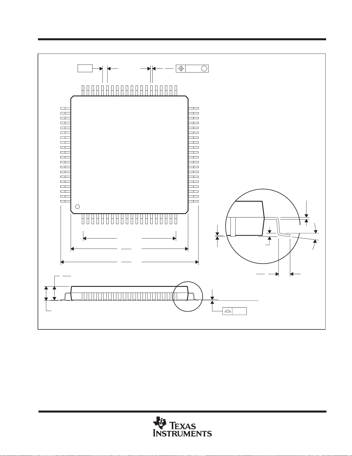
MECHANICAL DATA
http://www.xinpian.net
提供单片机解密、IC解密、芯片解密业务
010-62245566 13810019655
MTQF010A – JANUARY 1995 – REVISED DECEMBER 1996
PN (S-PQFP-G80) PLASTIC QUAD FLATPACK
61
80
1,45
1,35
0,50
60
1
9,50 TYP
12,20
SQ
11,80
14,20
SQ
13,80
0,27
0,17
20
41
0,08
M
40
21
0,05 MIN
0,13 NOM
Gage Plane
0,25
0°–7°
0,75
0,45
1,60 MAX
NOTES: A. All linear dimensions are in millimeters.
B. This drawing is subject to change without notice.
C. Falls within JEDEC MS-026
POST OFFICE BOX 655303 • DALLAS, TEXAS 75265
Seating Plane
0,08
4040135 /B 11/96
1
Page 98

IMPORTANTNOTICE
http://www.xinpian.net
提供单片机解密、IC解密、芯片解密业务
010-62245566 13810019655
TexasInstrumentsIncorporatedanditssubsidiaries(TI)reservetherighttomakecorrections,modifications,enhancements,
improvements,andotherchangestoitsproductsandservicesatanytimeandtodiscontinueanyproductorservicewithoutnotice.
Customersshouldobtainthelatestrelevantinformationbeforeplacingordersandshouldverifythatsuchinformationiscurrentand
complete.AllproductsaresoldsubjecttoTI’stermsandconditionsofsalesuppliedatthetimeoforderacknowledgment.
TIwarrantsperformanceofitshardwareproductstothespecificationsapplicableatthetimeofsaleinaccordancewithTI’s
standardwarranty.TestingandotherqualitycontroltechniquesareusedtotheextentTIdeemsnecessarytosupportthis
warranty.Exceptwheremandatedbygovernmentrequirements,testingofallparametersofeachproductisnotnecessarily
performed.
TIassumesnoliabilityforapplicationsassistanceorcustomerproductdesign.Customersareresponsiblefortheirproductsand
applicationsusingTIcomponents.Tominimizetherisksassociatedwithcustomerproductsandapplications,customersshould
provideadequatedesignandoperatingsafeguards.
TIdoesnotwarrantorrepresentthatanylicense,eitherexpressorimplied,isgrantedunderanyTIpatentright,copyright,mask
workright,orotherTIintellectualpropertyrightrelatingtoanycombination,machine,orprocessinwhichTIproductsorservices
areused.InformationpublishedbyTIregardingthird-partyproductsorservicesdoesnotconstitutealicensefromTItousesuch
productsorservicesorawarrantyorendorsementthereof.Useofsuchinformationmayrequirealicensefromathirdpartyunder
thepatentsorotherintellectualpropertyofthethirdparty,oralicensefromTIunderthepatentsorotherintellectualpropertyofTI.
ReproductionofTIinformationinTIdatabooksordatasheetsispermissibleonlyifreproductioniswithoutalterationandis
accompaniedbyallassociatedwarranties,conditions,limitations,andnotices.Reproductionofthisinformationwithalterationisan
unfairanddeceptivebusinesspractice.TIisnotresponsibleorliableforsuchaltereddocumentation.Informationofthirdparties
maybesubjecttoadditionalrestrictions.
ResaleofTIproductsorserviceswithstatementsdifferentfromorbeyondtheparametersstatedbyTIforthatproductorservice
voidsallexpressandanyimpliedwarrantiesfortheassociatedTIproductorserviceandisanunfairanddeceptivebusiness
practice.TIisnotresponsibleorliableforanysuchstatements.
TIproductsarenotauthorizedforuseinsafety-criticalapplications(suchaslifesupport)whereafailureoftheTIproductwould
reasonablybeexpectedtocauseseverepersonalinjuryordeath,unlessofficersofthepartieshaveexecutedanagreement
specificallygoverningsuchuse.Buyersrepresentthattheyhaveallnecessaryexpertiseinthesafetyandregulatoryramifications
oftheirapplications,andacknowledgeandagreethattheyaresolelyresponsibleforalllegal,regulatoryandsafety-related
requirementsconcerningtheirproductsandanyuseofTIproductsinsuchsafety-criticalapplications,notwithstandingany
applications-relatedinformationorsupportthatmaybeprovidedbyTI.Further,BuyersmustfullyindemnifyTIandits
representativesagainstanydamagesarisingoutoftheuseofTIproductsinsuchsafety-criticalapplications.
TIproductsareneitherdesignednorintendedforuseinmilitary/aerospaceapplicationsorenvironmentsunlesstheTIproductsare
specificallydesignatedbyTIasmilitary-gradeor"enhancedplastic."OnlyproductsdesignatedbyTIasmilitary-grademeetmilitary
specifications.BuyersacknowledgeandagreethatanysuchuseofTIproductswhichTIhasnotdesignatedasmilitary-gradeis
solelyattheBuyer'srisk,andthattheyaresolelyresponsibleforcompliancewithalllegalandregulatoryrequirementsin
connectionwithsuchuse.
TIproductsareneitherdesignednorintendedforuseinautomotiveapplicationsorenvironmentsunlessthespecificTIproducts
aredesignatedbyTIascompliantwithISO/TS16949requirements.Buyersacknowledgeandagreethat,iftheyuseany
non-designatedproductsinautomotiveapplications,TIwillnotberesponsibleforanyfailuretomeetsuchrequirements.
FollowingareURLswhereyoucanobtaininformationonotherTexasInstrumentsproductsandapplicationsolutions:
ProductsApplications
Amplifiersamplifier.ti.comAudiowww.ti.com/audio
DataConvertersdataconverter.ti.com Automotivewww.ti.com/automotive
DSPdsp.ti.com Broadbandwww.ti.com/broadband
Interfaceinterface.ti.com DigitalControlwww.ti.com/digitalcontrol
Logiclogic.ti.com Militarywww.ti.com/military
PowerMgmtpower.ti.com OpticalNetworkingwww.ti.com/opticalnetwork
Microcontrollersmicrocontroller.ti.com Securitywww.ti.com/security
RFIDwww.ti-rfid.com Telephonywww.ti.com/telephony
LowPowerwww.ti.com/lpw Video&Imagingwww.ti.com/video
Wireless
Wirelesswww.ti.com/wireless
MailingAddress:TexasInstruments,PostOfficeBox655303,Dallas,Texas75265
Copyright©2007,TexasInstrumentsIncorporated
 Loading...