

Page 1

MSP430x20x1, MSP430x20x2, MSP430x20x3
MIXED SIGNAL MICROCONTROLLER
SLAS491D -- AUGUST 2005 -- REVISED SEPTEMBER 2007
D Low Supply Voltage Range 1.8 V to 3.6 V
D Ultralow Power Consumption
-- Active Mode: 220 μAat1MHz,2.2V
-- Standby Mode: 0.5 μA
-- Off Mode (RAM Retention): 0.1 μA
D Five Power-Saving Modes
D Ultrafast Wake-Up From Standby Mode in
Less Than 1 μs
D 16-Bit RISC Architecture, 62.5 ns
Instruction Cycle Time
D Basic Clock Module Configurations:
-- Internal Frequencies up to 16 MHz With
Four Calibrated Frequencies to ±1%
-- Internal Very Low Power LF Oscillator
-- 32-kHz Crystal
-- External Digital Clock Source
D 16-Bit Timer_A With Two Capture/Compare
Registers
D On-Chip Comparator for Analog Signal
Compare Function or Slope A/D
(MSP430x20x1 only)
D 10-Bit 200-ksps A/D Converter With Internal
Reference, Sample-and-Hold, and Autoscan
(MSP430x20x2 only)
D 16-Bit Sigma-Delta A/D Converter With
Differential PGA Inputs and Internal
Reference (MSP430x20x3 only)
D Universal Serial Interface (USI) Supporting
SPI and I2C
(MSP430x20x2 and MSP430x20x3 only)
D Brownout Detector
D Serial Onboard Programming,
No External Programming Voltage Needed
Programmable Code Protection by
Security Fuse
D On-Chip Emulation Logic With Spy-Bi-Wire
Interface
D Family Members Include:
MSP430F2001: 1KB + 256B Flash Memory
128B RAM
MSP430F2011: 2KB + 256B Flash Memory
128B RAM
MSP430F2002: 1KB + 256B Flash Memory
128B RAM
MSP430F2012: 2KB + 256B Flash Memory
128B RAM
MSP430F2003: 1KB + 256B Flash Memory
128B RAM
MSP430F2013: 2KB + 256B Flash Memory
128B RAM
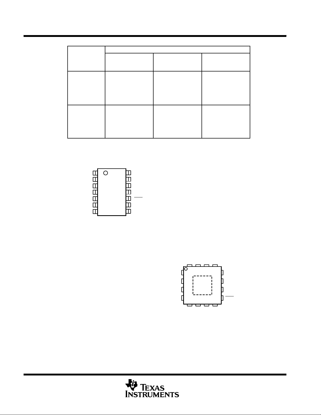
D Available in a 14-Pin Plastic Small-Outline
Thin Package (TSSOP), 14-Pin Plastic Dual
Inline Package (PDIP), and 16-Pin QFN
D For Complete Module Descriptions, See the
MSP430x2xx Family User’s Guide
description
The Texas Instruments MSP430 family of ultralow-power microcontrollers consist of several devices featuring
different sets of peripherals targeted for various applications. The architecture, combined with five low-power
modes is optimized to achieve extended battery life in portable measurement applications. The device features
a powerful 16-bit RISC CPU, 16-bit registers, and constant generators that contribute to maximum code
efficiency. The digitally controlled oscillator (DCO) allows wake-up from low-power modes to active mode in less
than 1μs.
The MSP430x20xx series is an ultralow-power mixed signal microcontroller with a built-in 16-bit timer, and ten
I/O pins. In addition the MSP430x20x1 has a versatile analog comparator. The MSP430x20x2 and
MSP430x20x3 have built-in communication capability using synchronous protocols (SPI or I2C), and a 10-bit
A/D converter (MSP430x20x2) or a 16-bit sigma-delta A/D converter (MSP430x20x3).
Typicalapplicationsinclude sensor systems that capture analog signals,convert them to digital values, and then
process the data for display or for transmission to a host system. Stand alone RF sensor front end is another
area of application.
Please be aware that an important notice concerning availability, standard warranty, and use in critical applications of
Texas Instruments semiconductor products and disclaimers thereto appears at the end of this data sheet.
PRODUCTION DATA information is current as of publication date.
Products conform to specifications per the terms of Texas Instruments
standard warranty. Production processing does not necessarily include
testing of all parameters.
POST OFFICE BOX 655303 • DALLAS, TEXAS 75265
Copyright © 2007 Texas Instruments Incorporated
1
Page 2
MSP430x20x1, MSP430x20x2, MSP430x20x3
MIXED SIGNAL MICROCONTROLLER
SLAS491D -- AUGUST 2005 -- REVISED SEPTEMBER 2007
AVAILABLE OPTIONS
T
A
-- 4 0 °Cto85°C
-- 4 0 °C to 105°C
device pinout, MSP430x20x1
PW or N PACKAGE
V
CC
P1.0/TACLK/ACLK/CA0
P1.1/TA0/CA1
P1.2/TA1/CA2
P1.3/CAOUT/CA3
P1.4/SMCLK/CA4/TCK
P1.5/TA0/CA5/TMS
(TOP VIEW)
1
2
3
4
5
6
7
PLASTIC
14-PIN TSSOP
(PW)
MSP430F2001IPW
MSP430F2011IPW
MSP430F2002IPW
MSP430F2012IPW
MSP430F2003IPW
MSP430F2013IPW
MSP430F2001TPW
MSP430F2011TPW
MSP430F2002TPW
MSP430F2012TPW
MSP430F2003TPW
MSP430F2013TPW
14
V
13
12
11
10
9
8
SS
XIN/P2.6/TA1
XOUT/P2.7
TEST/SBWTCK
RST
/NMI/SBWTDIO
P1.7/CAOUT/CA7/TDO/TDI
P1.6/TA1/CA6/TDI/TCLK
PACKAGED DEVICES
PLASTIC
14-PIN DIP
(N)
MSP430F2001IN
MSP430F2011IN
MSP430F2002IN
MSP430F2012IN
MSP430F2003IN
MSP430F2013IN
MSP430F2001TN
MSP430F2011TN
MSP430F2002TN
MSP430F2012TN
MSP430F2003TN
MSP430F2013TN
PLASTIC
16-PIN QFN
(RSA)
MSP430F2001IRSA
MSP430F2011IRSA
MSP430F2002IRSA
MSP430F2012IRSA
MSP430F2003IRSA
MSP430F2013IRSA
MSP430F2001TRSA
MSP430F2011TRSA
MSP430F2002TRSA
MSP430F2012TRSA
MSP430F2003TRSA
MSP430F2013TRSA
P1.0/TACLK/ACLK/CA0
P1.1/TA0/CA1
P1.2/TA1/CA2
P1.3/CAOUT/CA3
NOTE: See port schematics section for detailed I/O information.
RSA PACKAGE
(TOP VIEW)
CCVSS
V
NC
15
1
2
3
4
67
P1.5/TA0/CA5/TMS
P1.4/SMCLK/CA4/TCK
NC
14
12
11
10
9
P1.6/TA1/CA6/TDI/TCLK
P1.7/CAOUT/CA7/TDO/TDI
XIN/P2.6/TA1
XOUT/P2.7
TEST/SBWTCK
RST
/NMI/SBWTDIO
2
POST OFFICE BOX 655303 • DALLAS, TEXAS 75265
Page 3
device pinout, MSP430x20x2
V
P1.0/TACLK/ACLK/A0
P1.1/TA0/A1
P1.2/TA1/A2
P1.3/ADC10CLK/A3/VREF--/VeREF--
P1.4/SMCLK/A4/VREF+/VeREF+/TCK
P1.5/TA0/A5/SCLK/TMS
PW or N PACKAGE
(TOP VIEW)
1
CC
2
3
4
5
6
7
P1.3/ADC10CLK/A3/VREF--/VeREF--
14
13
12
11
10
MSP430x20x1, MSP430x20x2, MSP430x20x3
MIXED SIGNAL MICROCONTROLLER
V
SS
XIN/P2.6/TA1
XOUT/P2.7
TEST/SBWTCK
RST
/NMI/SBWTDIO
9
P1.7/A7/SDI/SDA/TDO/TDI
8
P1.6/TA1/A6/SDO/SCL/TDI/TCLK
P1.0/TACLK/ACLK/A0
P1.1/TA0/A1
P1.2/TA1/A2
SLAS491D -- AUGUST 2005 -- REVISED SEPTEMBER 2007
RSA PACKAGE
(TOP VIEW)
SS
DVCCDV
15
1
2
3
4
CC
AV
67
14
SS
AV
XIN/P2.6/TA1
12
XOUT/P2.7
11
10
TEST/SBWTCK
RST
9
/NMI/SBWTDIO
NOTE: See port schematics section for detailed I/O information.
P1.5/TA0/A5/SCLK/TMS
P1.7/A7/SDI/SDA/TDO/TDI
P1.6/TA1/A6/SDO/SCL/TDI/TCLK
P1.4/SMCLK/A4/VREF+/VeREF+/TCK
POST OFFICE BOX 655303 • DALLAS, TEXAS 75265
3
Page 4
MSP430x20x1, MSP430x20x2, MSP430x20x3
MIXED SIGNAL MICROCONTROLLER
SLAS491D -- AUGUST 2005 -- REVISED SEPTEMBER 2007
device pinout, MSP430x20x3
PW or N PACKAGE
(TOP VIEW)
V
CC
P1.0/TACLK/ACLK/A0+
P1.1/TA0/A0--/A4+
P1.2/TA1/A1+/A4--
P1.3/VREF/A1--
P1.4/SMCLK/A2+/TCK
P1.5/TA0/A2--/SCLK/TMS
1
2
3
4
5
6
7
14
13
12
11
10
V
SS
XIN/P2.6/TA1
XOUT/P2.7
TEST/SBWTCK
RST
/NMI/SBWTDIO
9
P1.7/A3--/SDI/SDA/TDO/TDI
8
P1.6/TA1/A3+/SDO/SCL/TDI/TCLK
P1.0/TACLK/ACLK/A0+
P1.1/TA0/A0--/A4+
P1.2/TA1/A1+/A4--
P1.3/VREF/A1--
RSA PACKAGE
(TOP VIEW)
SS
CC
DVCCDV
AV
15
1
2
3
4
14
67
SS
AV
XIN/P2.6/TA1
12
XOUT/P2.7
11
10
TEST/SBWTCK
RST
9
/NMI/SBWTDIO
NOTE: See port schematics section for detailed I/O information.
P1.4/SMCLK/A2+/TCK
P1.5/TA0/A2--/SCLK/TMS
P1.7/A3--/SDI/SDA/TDO/TDI
P1.6/TA1/A3+/SDO/SCL/TDI/TCLK
4
POST OFFICE BOX 655303 • DALLAS, TEXAS 75265
Page 5
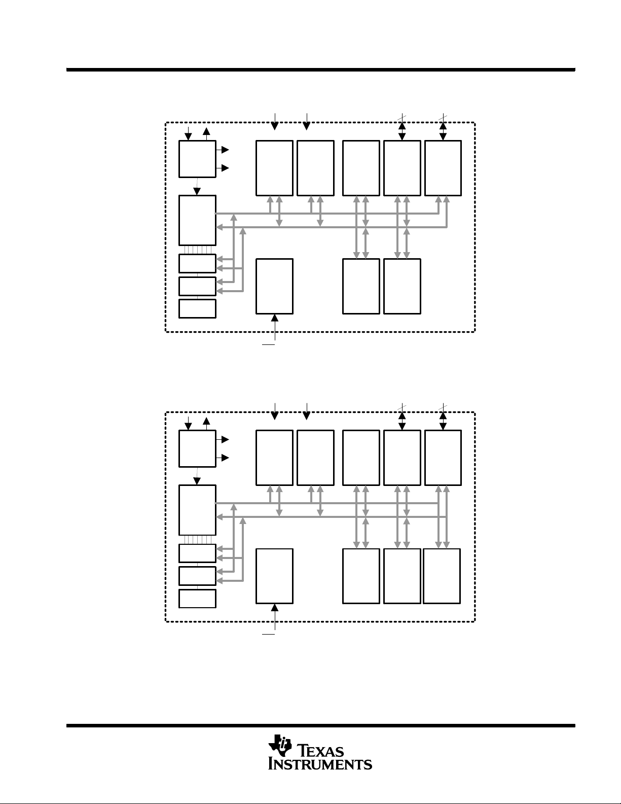
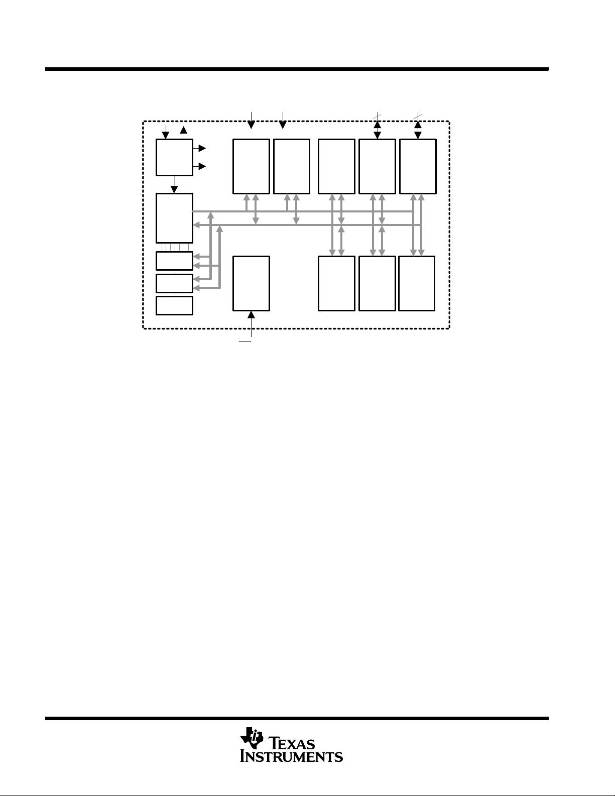
functional block diagram, MSP430x20x1
MSP430x20x1, MSP430x20x2, MSP430x20x3
MIXED SIGNAL MICROCONTROLLER
SLAS491D -- AUGUST 2005 -- REVISED SEPTEMBER 2007
VCC VSS
System+
16MHz
CPU
incl. 16
Registers
Emulation
(2BP)
JTAG
Interface
XOUT
MCLK
ACLK
SMCLK
MAB
MDB
Flash
2kB
1kB
Brownout
Protection
RST/NMI
XIN
Basic Clock
Spy--Bi Wire
NOTE: See port schematics section for detailed I/O information.
functional block diagram, MSP430x20x2
VCC VSS
System+
16MHz
CPU
incl. 16
Registers
XOUT
MCLK
ACLK
SMCLK
MAB
MDB
Flash
2kB
1kB
XIN
Basic Clock
RAM
128B
128B
RAM
128B
128B
Comparator
_A+
8 channel
input mux
Watchdog
WDT+
15/16--Bit
ADC10
10--bit
8 Channels
Autoscan
DTC
P1.x & JTAG
8 2
Port P1
8I/O
Interrupt
capability,
pull--up/down
resistors
Timer_A2
2CC
Registers
P1.x & JTAG
8 2
Port P1
8I/O
Interrupt
capability,
pull--up/down
resistors
P2.x &
XIN/XOUT
Port P2
2I/O
Interrupt
capability,
pull--up/down
resistors
P2.x &
XIN/XOUT
Port P2
2I/O
Interrupt
capability,
pull--up/down
resistors
Emulation
(2BP)
JTAG
Interface
Spy--Bi Wire
Brownout
Protection
RST/NMI
NOTE: See port schematics section for detailed I/O information.
POST OFFICE BOX 655303 • DALLAS, TEXAS 75265
Watchdog
WDT+
15/16--Bit
Timer_A2
2CC
Registers
USI
Universal
Serial
Interface
SPI, I2C
5
Page 6
MSP430x20x1, MSP430x20x2, MSP430x20x3
MIXED SIGNAL MICROCONTROLLER
SLAS491D -- AUGUST 2005 -- REVISED SEPTEMBER 2007
functional block diagram, MSP430x20x3
VCC VSS
System+
16MHz
CPU
incl. 16
Registers
Emulation
(2BP)
JTAG
Interface
XOUT
MCLK
ACLK
SMCLK
MAB
MDB
Flash
2kB
1kB
Brownout
Protection
RST/NMI
RAM
128B
128B
XIN
Basic Clock
Spy--Bi Wire
NOTE: See port schematics section for detailed I/O information.
SD16_A
16--bit
Sigma-Delta A/D
Converter
Watchdog
WDT+
15/16--Bit
P1.x & JTAG
8 2
Port P1
8I/O
Interrupt
capability,
pull--up/down
resistors
Timer_A2
2CC
Registers
P2.x &
XIN/XOUT
Port P2
2I/O
Interrupt
capability,
pull--up/down
resistors
USI
Universal
Serial
Interface
SPI, I2C
6
POST OFFICE BOX 655303 • DALLAS, TEXAS 75265
Page 7
MSP430x20x1, MSP430x20x2, MSP430x20x3
DESCRIPTION
MIXED SIGNAL MICROCONTROLLER
SLAS491D -- AUGUST 2005 -- REVISED SEPTEMBER 2007
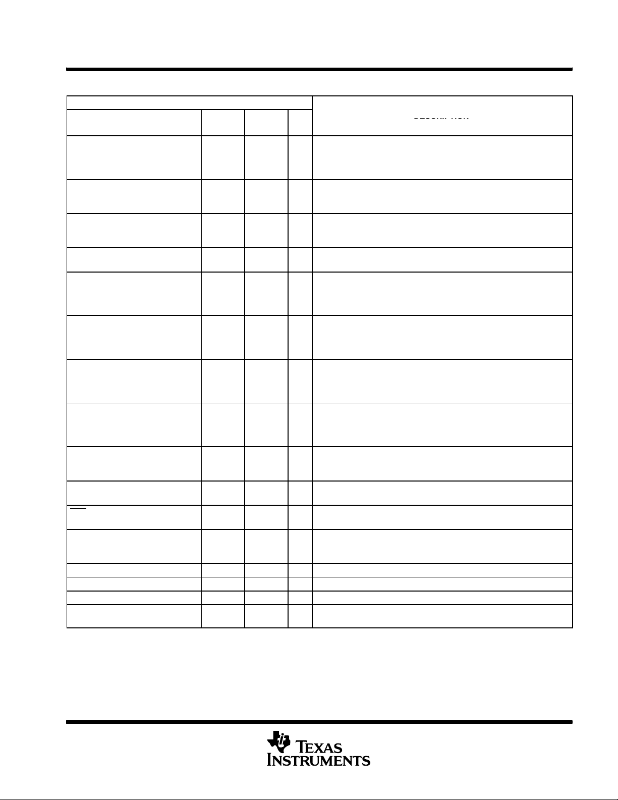
Terminal Functions, MSP430x20x1
TERMINAL
NAME
P1.0/TACLK/ACLK/CA0 2 1 I/O General-purpose digital I/O pin
P1.1/TA0/CA1 3 2 I/O General-purpose digital I/O pin
P1.2/TA1/CA2 4 3 I/O General-purpose digital I/O pin
P1.3/CAOUT/CA3 5 4 I/O General-purpose digital I/O pin
P1.4/SMCLK/C4/TCK 6 5 I/O General-purpose digital I/O pin
P1.5/TA0/CA5/TMS 7 6 I/O General-purpose digital I/O pin
P1.6/TA1/CA6/TDI/TCLK 8 7 I/O General-purpose digital I/O pin
P1.7/CAOUT/CA7/TDO/TDI
XIN/P2.6/TA1 13 12 I/O Input terminal of crystal oscillator
XOUT/P2.7 12 11 I/O Output terminal of crystal oscillator
RST/NMI/SBWTDIO 10 9 I Reset or nonmaskable interrupt input
TEST/SBWTCK 11 10 I Selects test mode for JTAG pins on Port1. The device protection fuse is
V
CC
V
SS
NC NA 13, 15 Not connected
QFN Pad NA Package
†
TDO or TDI is selected via JTAG instruction.
NOTE: If XOUT/P2.7 is used as an input, excess current will flow until P2SEL.7 is cleared. This is due to the oscillator output driver connection
to this pad after reset.
†
PW or N RSA
NO. NO.
9 8 I/O General-purpose digital I/O pin
1 16 Supply voltage
14 14 Ground reference
Pad
I/O
Timer_A, clock signal TACLK input
ACLK signal ouput
Comparator_A+, CA0 input
Timer_A, capture: CCI0A input, compare: Out0 output
Comparator_A+, CA1 input
Timer_A, capture: CCI1A input, compare: Out1 output
Comparator_A+, CA2 input
Comparator_A+, output / CA3 input
SMCLK signal output
Comparator_A+, CA4 input
JTAG test clock, input terminal for device programming and test
Timer_A, compare: Out0 output
Comparator_A+, CA5 input
JTAG test mode select, input terminal for device programming and test
Timer_A, compare: Out1 output
Comparator_A+, CA6 input
JTAG test data input or test clock input during programming and test
Comparator_A+, output / CA7 input
JTAGtestdataoutputterminalortestdata input during programming and
test
General-purpose digital I/O pin
Timer_A, compare: Out1 output
General-purpose digital I/O pin
Spy-Bi-Wire test data input/output during programming and test
connected to TEST.
Spy-Bi-Wire test clock input during programming and test
NA QFN package pad connection to VSSrecommended.
DESCRIPTION
POST OFFICE BOX 655303 • DALLAS, TEXAS 75265
7
Page 8

MSP430x20x1, MSP430x20x2, MSP430x20x3
DESCRIPTION
MIXED SIGNAL MICROCONTROLLER
SLAS491D -- AUGUST 2005 -- REVISED SEPTEMBER 2007
Terminal Functions, MSP430x20x2
TERMINAL
NAME
P1.0/TACLK/ACLK/A0 2 1 I/O General-purpose digital I/O pin
P1.1/TA0/A1 3 2 I/O General-purpose digital I/O pin
P1.2/TA1/A2 4 3 I/O General-purpose digital I/O pin
P1.3/ADC10CLK/
A3/VREF--/VeREF--
P1.4/SMCLK/A4/VREF+/VeREF+/
TCK
P1.5/TA0/A5/SCLK/TMS 7 6 I/O General-purpose digital I/O pin
P1.6/TA1/A6/SDO/SCL/TDI/TCLK 8 7 I/O General-purpose digital I/O pin
P1.7/A7/SDI/SDA/TDO/TDI
XIN/P2.6/TA1 13 12 I/O Input terminal of crystal oscillator
XOUT/P2.7 12 11 I/O Output terminal of crystal oscillator
RST/NMI/SBWTDIO 10 9 I Reset or nonmaskable interrupt input
TEST/SBWTCK 11 10 I Selects test mode for JTAG pins on Port1. The device protection fuse is
V
CC
V
SS
†
TDO or TDI is selected via JTAG instruction.
NOTE: If XOUT/P2.7 is used as an input, excess current will flow until P2SEL.7 is cleared. This is due to the oscillator output driver connection
to this pad after reset.
†
PW, or N RSA
NO. NO.
5 4 I/O General-purpose digital I/O pin
6 5 I/O General-purpose digital I/O pin
9 8 I/O General-purpose digital I/O pin
1 NA Supply voltage
14 NA Ground reference
I/O
Timer_A, clock signal TACLK input
ACLK signal ouput
ADC10 analog input A0
Timer_A, capture: CCI0A input, compare: Out0 output
ADC10 analog input A1
Timer_A, capture: CCI1A input, compare: Out1 output
ADC10 analog input A2
ADC10 conversion clock output
ADC10 analog input A3
Input for negative external reference voltage/negative internal reference
voltage output
SMCLK signal output
ADC10 analog input A4
Input for positive external reference voltage/positive internal reference
voltage output
JTAG test clock, input terminal for device programming and test
Timer_A, compare: Out0 output
ADC10 analog input A5
USI: external clock input in SPI or I2C mode; clock output in SPI mode
JTAG test mode select, input terminal for device programming and test
Timer_A, capture: CCI1B input, compare: Out1 output
ADC10 analog input A6
USI: Data output in SPI mode; I2C clock in I2C mode
JTAG test data input or test clock input during programming and test
ADC10 analog input A7
USI: Data input in SPI mode; I2C data in I2C mode
JTAGtestdataoutputterminalortestdata input during programming and
test
General-purpose digital I/O pin
Timer_A, compare: Out1 output
General-purpose digital I/O pin
Spy-Bi-Wire test data input/output during programming and test
connected to TEST.
Spy-Bi-Wire test clock input during programming and test
DESCRIPTION
8
POST OFFICE BOX 655303 • DALLAS, TEXAS 75265
Page 9
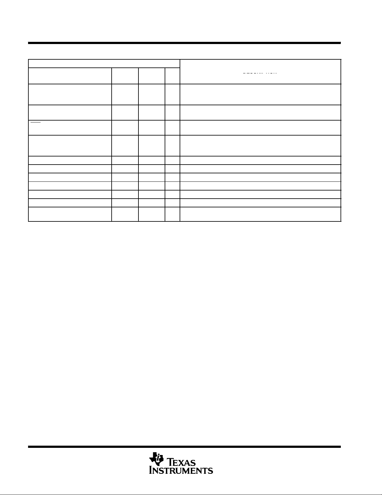
MSP430x20x1, MSP430x20x2, MSP430x20x3
DESCRIPTION
DESCRIPTION
MIXED SIGNAL MICROCONTROLLER
SLAS491D -- AUGUST 2005 -- REVISED SEPTEMBER 2007
Terminal Functions, MSP430x20x2 (Continued)
TERMINAL
NAME
DV
CC
AV
CC
DV
SS
AV
SS
QFN Pad NA Package
TERMINAL
NAME
P1.0/TACLK/ACLK/A0+ 2 1 I/O General-purpose digital I/O pin
P1.1/TA0/A0--/A4+ 3 2 I/O General-purpose digital I/O pin
P1.2/TA1/A1+/A4-- 4 3 I/O General-purpose digital I/O pin
P1.3/VREF/A1-- 5 4 I/O General-purpose digital I/O pin
P1.4/SMCLK/A2+/TCK 6 5 I/O General-purpose digital I/O pin
P1.5/TA0/A2--/SCLK/TMS 7 6 I/O General-purpose digital I/O pin
P1.6/TA1/A3+/SDO/SCL/TDI/TCLK 8 7 I/O General-purpose digital I/O pin
P1.7/A3--/SDI/SDA/TDO/TDI
†
TDO or TDI is selected via JTAG instruction.
†
PW, or N RSA
NO. NO.
NA 16 Digital supply voltage
NA 15 Analog supply voltage
NA 14 Digital ground reference
NA 13 Analog ground reference
Pad
I/O
NA QFN package pad connection to VSSrecommended.
Terminal Functions, MSP430x20x3
PW, or N RSA
NO. NO.
9 8 I/O General-purpose digital I/O pin
I/O
Timer_A, clock signal TACLK input
ACLK signal ouput
SD16_A positive analog input A0
Timer_A, capture: CCI0A input, compare: Out0 output
SD16_A negative analog input A0
SD16_A positive analog input A4
Timer_A, capture: CCI1A input, compare: Out1 output
SD16_A positive analog input A1
SD16_A negative analog input A4
Input for an external reference voltage/internal reference voltage output
(can be used as mid-voltage)
SD16_A negative analog input A1
SMCLK signal output
SD16_A positive analog input A2
JTAG test clock, input terminal for device programming and test
Timer_A, compare: Out0 output
SD16_A negative analog input A2
USI: external clock input in SPI or I2C mode; clock output in SPI mode
JTAG test mode select, input terminal for device programming and test
Timer_A, capture: CCI1B input, compare: Out1 output
SD16_A positive analog input A3
USI: Data output in SPI mode; I2C clock in I2C mode
JTAG test data input or test clock input during programming and test
SD16_A negative analog input A3
USI: Data input in SPI mode; I2C data in I2C mode
JTAGtestdataoutputterminalortestdata input during programming and
test
DESCRIPTION
DESCRIPTION
POST OFFICE BOX 655303 • DALLAS, TEXAS 75265
9
Page 10
MSP430x20x1, MSP430x20x2, MSP430x20x3
DESCRIPTION
MIXED SIGNAL MICROCONTROLLER
SLAS491D -- AUGUST 2005 -- REVISED SEPTEMBER 2007
Terminal Functions, MSP430x20x3 (Continued)
TERMINAL
NAME
XIN/P2.6/TA1 13 12 I/O Input terminal of crystal oscillator
XOUT/P2.7 12 11 I/O Output terminal of crystal oscillator
RST/NMI/SBWTDIO 10 9 I Reset or nonmaskable interrupt input
TEST/SBWTCK 11 10 I Selects test mode for JTAG pins on Port1. The device protection fuse is
V
CC
V
SS
DV
CC
AV
CC
DV
SS
AV
SS
QFN Pad NA Package
NOTE: If XOUT/P2.7 is used as an input, excess current will flow until P2SEL.7 is cleared. This is due to the oscillator output driver connection
to this pad after reset.
PW, or N RSA
NO. NO.
1 NA Supply voltage
14 NA Ground reference
NA 16 Digital supply voltage
NA 15 Analog supply voltage
NA 14 Digital ground reference
NA 13 Analog ground reference
Pad
I/O
General-purpose digital I/O pin
Timer_A, compare: Out1 output
General-purpose digital I/O pin
Spy-Bi-Wire test data input/output during programming and test
connected to TEST.
Spy-Bi-Wire test clock input during programming and test
NA QFN package pad connection to VSSrecommended.
DESCRIPTION
10
POST OFFICE BOX 655303 • DALLAS, TEXAS 75265
Page 11
short-form description
CPU
MSP430x20x1, MSP430x20x2, MSP430x20x3
MIXED SIGNAL MICROCONTROLLER
SLAS491D -- AUGUST 2005 -- REVISED SEPTEMBER 2007
The MSP430 CPU has a 16-bit RISC architecture
that is highly transparent to the application. All
operations, other than program-flow instructions,
are performed as register operations in
conjunction with seven addressing modes for
source operand and four addressing modes for
destination operand.
The CPU is integrated with 16 registers that
provide reduced instruction execution time. The
register-to-register operation execution time is
one cycle of the CPU clock.
Four of the registers, R0 to R3, are dedicated as
program counter, stack pointer, status register,
and constant generator respectively. The
remaining registers are general-purpose
registers.
Peripherals are connected to the CPU using data,
address, and control buses, and can be handled
with all instructions.
instruction set
The instruction set consists of 51 instructions with
three formats and seven address modes. Each
instruction can operate on word and byte data.
Table 1 shows examples of the three types of
instruction formats; the address modes are listed
in Table 2.
Program Counter
Stack Pointer
Status Register
Constant Generator
General-Purpose Register
General-Purpose Register
General-Purpose Register
General-Purpose Register
General-Purpose Register
General-Purpose Register
General-Purpose Register
General-Purpose Register
General-Purpose Register
General-Purpose Register
General-Purpose Register
General-Purpose Register
PC/R0
SP/R1
SR/CG1/R2
CG2/R3
R4
R5
R6
R7
R8
R9
R10
R11
R12
R13
R14
R15
Table 1. Instruction Word Formats
Dual operands, source-destination e.g., ADD R4,R5 R4 + R5 ------> R5
Single operands, destination only e.g., CALL R8 PC -- -->(TOS), R8----> PC
Relative jump, un/conditional e.g., JNE Jump-on-equal bit = 0
Table 2. Address Mode Descriptions
ADDRESS MODE S D SYNTAX EXAMPLE OPERATION
Register F
Indexed F F MOV X(Rn),Y(Rm) MOV 2(R5),6(R6) M(2+R5)----> M(6+R6)
Symbolic (PC relative) F F MOV EDE,TONI M(EDE) ----> M(TONI)
Absolute F F MOV &MEM,&TCDAT M(MEM) ----> M(TCDAT)
Indirect F MOV @Rn,Y(Rm) MOV @R10,Tab(R6) M(R10) ----> M(Tab+R6)
Indirect
autoincrement
Immediate F MOV #X,TONI MOV #45,TONI #45 ----> M(TONI)
NOTE: S = source D = destination
F
F MOV @Rn+,Rm MOV @R10+,R11
MOV Rs,Rd MOV R10,R11 R10 ----> R11
M(R10) ----> R11
R10 + 2----> R10
POST OFFICE BOX 655303 • DALLAS, TEXAS 75265
11
Page 12

MSP430x20x1, MSP430x20x2, MSP430x20x3
MIXED SIGNAL MICROCONTROLLER
SLAS491D -- AUGUST 2005 -- REVISED SEPTEMBER 2007
operating modes
The MSP430 has one active mode and five software-selectable low-power modes of operation. An interrupt
event can wake up the device from any of the five low-power modes, s ervice the request, and restore back to
the low-power mode on return from the interrupt program.
The following six operating modes can be configured by software:
D Active mode AM;
-- All clocks are active
D Low-power mode 0 (LPM0);
-- CPU is disabled
ACLK and SMCLK remain active. MCLK is disabled
D Low-power mode 1 (LPM1);
-- CPU is disabled
ACLK and SMCLK remain active. MCLK is disabled
DCO’s dc-generator is disabled if DCO not used in active mode
D Low-power mode 2 (LPM2);
-- CPU is disabled
MCLK and SMCLK are disabled
DCO’s dc-generator remains enabled
ACLK remains active
D Low-power mode 3 (LPM3);
-- CPU is disabled
MCLK and SMCLK are disabled
DCO’s dc-generator is disabled
ACLK remains active
D Low-power mode 4 (LPM4);
-- CPU is disabled
ACLK is disabled
MCLK and SMCLK are disabled
DCO’s dc-generator is disabled
Crystal oscillator is stopped
12
POST OFFICE BOX 655303 • DALLAS, TEXAS 75265
Page 13
MSP430x20x1, MSP430x20x2, MSP430x20x3
MIXED SIGNAL MICROCONTROLLER
SLAS491D -- AUGUST 2005 -- REVISED SEPTEMBER 2007
interrupt vector addresses
The interrupt vectors and the power-up starting address are located in the address range of 0FFFFh--0FFC0h.
The vector contains the 16-bit address of the appropriate interrupt handler instruction sequence.
If the reset vector (located at address 0FFFEh) contains 0FFFFh (e.g., flash is not programmed) the CPU will
go into LPM4 immediately after power-up.
INTERRUPT SOURCE INTERRUPT FLAG SYSTEM INTERRUPT WORD ADDRESS PRIORITY
Power-up
External reset
Watchdog Timer+
Flash key violation
PC out-of-range (see Note 1)
NMI
Oscillator fault
Flash memory access violation
Comparator_A+ (MSP430x20x1 only) CAIFG(seeNote3) maskable 0FFF6h 27
Watchdog Timer+ WDTIFG maskable 0FFF4h 26
Timer_A2 TACCR0 CCIFG (see Note 3) maskable 0FFF2h 25
Timer_A2
ADC10 (MSP430x20x2 only)
SD16_A (MSP430x20x3 only)
USI
(MSP430x20x2, MSP430x20x3 only)
I/O Port P2
(two flags)
I/O Port P1
(eight flags)
(see Note 5) 0FFDEh ... 0FFC0h 15 ... 0, lowest
NOTES: 1. A reset is generated if the CPU tries to fetch instructions from within the module register memory address range (0h--01FFh) or from
within unused address ranges.
2. Multiple source flags
3. Interrupt flags are located in the module
4. (non)-maskable: the individual interrupt-enable bit can disable an interrupt event, but the general interrupt enable cannot.
5. The interrupt vectors at addresses 0FFDEh to 0FFC0h are not used in this device and can be used for regular program code if
necessary.
TAIFG (see Notes 2 and 3)
SD16CCTL0 SD16OVIFG,
PORIFG
RSTIFG
WDTIFG
KEYV
(see Note 2)
NMIIFG
OFIFG
ACCVIFG
(see Notes 2 and 4)
TACCR1 CCIFG.
ADC10IFG (see Note 3)
SD16CCTL0 SD16IFG
(see Notes 2 and 3)
USIIFG, USISTTIFG
(see Notes 2 and 3)
P2IFG.6toP2IFG.7
(see Notes 2 and 3)
P1IFG.0toP1IFG.7
(see Notes 2 and 3)
Reset 0FFFEh 31, highest
(non)-maskable,
(non)-maskable,
(non)-maskable
maskable 0FFF0h 24
maskable
maskable
maskable 0FFE8h 20
maskable 0FFE6h 19
maskable 0FFE4h 18
0FFFCh 30
0FFFAh 29
0FFF8h 28
0FFEEh 23
0FFECh 22
0FFEAh 21
0FFE2h 17
0FFE0h 16
POST OFFICE BOX 655303 • DALLAS, TEXAS 75265
13
Page 14
MSP430x20x1, MSP430x20x2, MSP430x20x3
MIXED SIGNAL MICROCONTROLLER
SLAS491D -- AUGUST 2005 -- REVISED SEPTEMBER 2007
special function registers
Most interrupt and module enable bits are collected into the lowest address space. Special function register bits
not allocated to a functional purpose are not physically present in the device. Simple software access is provided
with this arrangement.
interrupt enable 1 and 2
Address
0h
7654 0
NMIIEACCVIE
rw-0 rw-0 rw-0
32 1
OFIE WDTIE
rw-0
WDTIE: WatchdogTimer interrupt enable. Inactive if watchdog mode is selected. Active if WatchdogTimer
is configured in interval timer mode.
OFIE: Oscillator fault enable
NMIIE: (Non)maskable interrupt enable
ACCVIE: Flash access violation interrupt enable
Address
01h
7654 032 1
interrupt flag register 1 and 2
Address
02h NMIIFG
7654 0
rw-0 rw-1 rw-(0)
32 1
RSTIFG
rw-(0)
PORIFG
rw-(1)
OFIFG WDTIFG
WDTIFG: Set on Watchdog Timer overflow (in watchdog mode) or security key violation.
Reset on V
power-up or a reset condition at RST/NMI pin in reset mode.
CC
OFIFG: Flag set on oscillator fault
RSTIFG: External reset interrupt flag. Set on a reset condition at RST
/NMI pin in reset mode. Reset on V
power-up
PORIFG: Power-On Reset interrupt flag. Set on V
NMIIFG: Set via RST
/NMI-pin
power-up.
CC
CC
14
Address
03h
Legend rw:
rw-0,1:
rw-(0,1):
7654 032 1
Bit can be read and written.
Bit can be read and written. It is Reset or Set by PUC.
Bit can be read and written. It is Reset or Set by POR.
SFR bit is not present in device
POST OFFICE BOX 655303 • DALLAS, TEXAS 75265
Page 15
MSP430x20x1, MSP430x20x2, MSP430x20x3
MIXED SIGNAL MICROCONTROLLER
SLAS491D -- AUGUST 2005 -- REVISED SEPTEMBER 2007
memory organization
MSP430F200x MSP430F201x
Memory
Main: interrupt vector
Main: code memory
Information memory Size
RAM Size 128 Byte
Peripherals 16-bit
flash memory
The flash memory can be programmed via the Spy-Bi-Wire/JTAG port, or in-system by the CPU. The CPU can
perform single-byte and single-word writes to the flash memory. Features of the flash memory include:
D Flash memory has n segments of main memory and four segments of information memory (A to D) of 64
bytes each. Each segment in main memory is 512 bytes in size.
Size
Flash
Flash
Flash
8-bit
8-bit SFR
1KB Flash
0FFFFh--0FFC0h
0FFFFh--0FC00h
256 Byte
010FFh -- 01000h
027Fh -- 0200h
01FFh -- 0100h
0FFh -- 010h
0Fh -- 00h
2KB Flash
0FFFFh--0FFC0h
0FFFFh--0F800h
256 Byte
010FFh -- 01000h
128 Byte
027Fh -- 0200h
01FFh -- 0100h
0FFh -- 010h
0Fh -- 00h
D Segments 0 to n may be erased in one step, or each segment may be individually erased.
D Segments A to D can be erased individually, or as a group with segments 0 --n.
Segments A to D are also called information memory.
D Segment A contains calibration data. After reset segment A is protected against programming and erasing.
It can be unlocked but care should be taken not to erase this segment if the device-specific calibration data
is required.
POST OFFICE BOX 655303 • DALLAS, TEXAS 75265
15
Page 16
MSP430x20x1, MSP430x20x2, MSP430x20x3
MIXED SIGNAL MICROCONTROLLER
SLAS491D -- AUGUST 2005 -- REVISED SEPTEMBER 2007
peripherals
Peripherals are connected to the CPU through data, address, and control busses and can be handled using
all instructions. For complete module descriptions, refer to the MSP430x2xx Family User’s Guide.
oscillator and system clock
The clock system is supported by the basic clock module that includes support for a 32768-Hz watch crystal
oscillator, an internal very-low-power low-frequency oscillator and an internal digitally-controlled oscillator
(DCO). The basic clock module is designed to meet the requirements of both low system cost and low power
consumption. The internal DCO provides a fast turn-on clock source and stabilizes in less than 1 μs. The basic
clock module provides the following clock signals:
D Auxiliary clock (ACLK), sourced either from a 32768-Hz watch crystal or the internal LF oscillator.
D Main clock (MCLK), the system clock used by the CPU.
D Sub-Main clock (SMCLK), the sub-system clock used by the peripheral modules.
DCO Calibration Data (provided from factory in flash info memory segment A)
DCO Frequency Calibration Register Size Address
1MHz
8MHz
12 MHz
16 MHz
CALBC1_1MHZ byte
CALDCO_1MHZ byte
CALBC1_8MHZ byte
CALDCO_8MHZ byte
CALBC1_12MHZ byte
CALDCO_12MHZ byte
CALBC1_16MHZ byte
CALDCO_16MHZ byte
010FFh
010FEh
010FDh
010FCh
010FBh
010FAh
010F9h
010F8h
brownout
The brownout circuit is implemented to provide the proper internal reset signal to the device during power on
and power off.
digital I/O
There is one 8-bit I/O port implemented—port P1—and two bits of I/O port P2:
D All individual I/O bits are independently programmable.
D Any combination of input, output, and interrupt condition is possible.
D Edge-selectable interrupt input capability for all the eight bits of port P1 and the two bits of port P2.
D Read/write access to port-control registers is supported by all instructions.
D Each I/O has an individually programmable pull-up/pull-down resistor.
WDT+ watchdog timer
The primary function of the watchdog timer (WDT+) module is to perform a controlled system restart after a
software problem occurs. If the selected time interval expires, a system reset is generated. If the watchdog
function is not needed in an application, the module can be disabled or configured as an interval timer and can
generate interrupts at selected time intervals.
16
POST OFFICE BOX 655303 • DALLAS, TEXAS 75265
Page 17
MSP430x20x1, MSP430x20x2, MSP430x20x3
A
A
MIXED SIGNAL MICROCONTROLLER
SLAS491D -- AUGUST 2005 -- REVISED SEPTEMBER 2007
timer_A2
Timer_A2 is a 16-bit timer/counter with two capture/compare registers. Timer_A2 can support multiple
capture/compares, PWM outputs, and interval timing. Timer_A2 also has extensive interrupt capabilities.
Interrupts may be generated from the c ounter on overflow conditions and from each of the capture/compare
registers.
Timer_A2 Signal Connections (MSP43020x1 only)
Input
Pin Number
PW, N RSA PW, N RSA
2-P1.0 1-P1.0 TACLK TAC L K
2-P1.0 1-P1.0 TACLK INCLK
3-P1.1 2-P1.1 TA0 CCI0A
4-P1.2 3-P1.2 TA1 CCI1A
Device
Input Signal
ACLK ACLK
SMCLK SMCLK
ACLK (internal) CCI0B
V
SS
V
CC
CAOUT (internal) CCI1B
V
SS
V
CC
Module
Input Name
GND
V
CC
GND
V
CC
Module
Block
Timer N
CCR0 TA0
CCR1 TA1
Module
Output Signal
Output
Pin Number
3-P1.1 2-P1.1
7-P1.5 6-P1.5
4-P1.2 3-P1.2
8-P1.6 7-P1.6
13 - P2.6 12 - P2.6
Timer_A2 Signal Connections (MSP430F20x2, MSP430F20x3)
Input
Pin Number
PW, N RSA PW, N RSA
2-P1.0 1-P1.0 TACLK TAC L K
2-P1.0 1-P1.0 TACLK INCLK
3-P1.1 2-P1.1 TA0 CCI0A
7-P1.5 6-P1.5 ACLK (internal) CCI0B
4-P1.2 3-P1.2 TA1 CCI1A
8-P1.6 7-P1.6 TA1 CCI1B
Device
Input Signal
ACLK ACLK
SMCLK SMCLK
V
SS
V
CC
V
SS
V
CC
Module
Input Name
GND
V
CC
GND
V
CC
Module
Block
Timer N
CCR0 TA0
CCR1 TA1
Module
Output Signal
Output
Pin Number
3-P1.1 2-P1.1
7-P1.5 6-P1.5
4-P1.2 3-P1.2
8-P1.6 7-P1.6
13 - P2.6 12 - P2.6
comparator_A+ (MSP430x20x1 only)
The primary function of the comparator_A+ module is to support precision slope analog-to-digital conversions,
battery-voltage supervision, and monitoring of external analog signals.
POST OFFICE BOX 655303 • DALLAS, TEXAS 75265
17
Page 18

MSP430x20x1, MSP430x20x2, MSP430x20x3
MIXED SIGNAL MICROCONTROLLER
SLAS491D -- AUGUST 2005 -- REVISED SEPTEMBER 2007
USI (MSP430x20x2 and MSP430x20x3 only)
The universal serial interface (USI) module is used for serial data communication and provides the basic
hardware for synchronous communication protocols like SPI and I2C.
ADC10 (MSP430x20x2 only)
The ADC10 module supports fast, 10-bit analog-to-digital conversions. The module implements a 10-bit SAR
core, sample select control, reference generator and data transfer controller, or DTC, for automatic conversion
result handling, allowing ADC samples to be converted and stored without any CPU intervention.
SD16_A (MSP430x20x3 only)
The SD16_A module supports 16-bit analog-to-digital conversions. The module implements a 16-bit
sigma-delta core and reference generator. In addition to external analog inputs, internal V
temperature sensors are also available.
CC
sense and
18
POST OFFICE BOX 655303 • DALLAS, TEXAS 75265
Page 19
peripheral file map
ADC10 (MSP430x20x2 only) ADC control 0
SD16_A (MSP430x20x3 only) General Control
Timer_A Capture/compare register
Flash Memory Flash control 3
Watchdog Timer+ Watchdog/timer control WDTCTL 0120h
ADC10 (MSP430x20x2 only) Analog enable ADC10AE 04Ah
SD16_A (MSP430x20x3 only) Channel 0 Input Control
USI
(MSP430x20x2 and
MSP430x20x3 only)
Comparator_A+
(MSP430x20x1 only)
Basic Clock System+ Basic clock system control 3
Port P2 Port P2 resistor enable
Port P1 Port P1 resistor enable
Special Function SFR interrupt flag 2
MSP430x20x1, MSP430x20x2, MSP430x20x3
MIXED SIGNAL MICROCONTROLLER
SLAS491D -- AUGUST 2005 -- REVISED SEPTEMBER 2007
PERIPHERALS WITH WORD ACCESS
ADC control 1
ADC memory
Channel 0 Control
Interrupt vector word register
Channel 0 conversion memory
Capture/compare register
Timer_A register
Capture/compare control
Capture/compare control
Timer_A control
Timer_A interrupt vector
Flash control 2
Flash control 1
PERIPHERALS WITH BYTE ACCESS
Analog Enable
USI control 0
USI control 1
USI clock control
USI bit counter
USI shift register
Comparator_A+ port disable
Comparator_A+ control 2
Comparator_A+ control 1
Basic clock system control 2
Basic clock system control 1
DCO clock frequency control
Port P2 selection
Port P2 interrupt enable
Port P2 interrupt edge select
Port P2 interrupt flag
Port P2 direction
Port P2 output
Port P2 input
Port P1 selection
Port P1 interrupt enable
Port P1 interrupt edge select
Port P1 interrupt flag
Port P1 direction
Port P1 output
Port P1 input
SFR interrupt flag 1
SFR interrupt enable 2
SFR interrupt enable 1
ADC10CTL0
ADC10CTL0
ADC10MEM
SD16CTL
SD16CCTL0
SD16IV
SD16MEM0
TACCR1
TACCR0
TAR
TACCTL1
TACCTL0
TAC T L
TAI V
FCTL3
FCTL2
FCTL1
SD16INCTL0
SD16AE
USICTL0
USICTL1
USICKCTL
USICNT
USISR
CAPD
CACTL2
CACTL1
BCSCTL3
BCSCTL2
BCSCTL1
DCOCTL
P2REN
P2SEL
P2IE
P2IES
P2IFG
P2DIR
P2OUT
P2IN
P1REN
P1SEL
P1IE
P1IES
P1IFG
P1DIR
P1OUT
P1IN
IFG2
IFG1
IE2
IE1
01B0h
01B2h
01B4h
0100h
0102h
0110h
0112h
0174h
0172h
0170h
0164h
0162h
0160h
012Eh
012Ch
012Ah
0128h
0B0h
0B7h
078h
079h
07Ah
07Bh
07Ch
05Bh
05Ah
059h
053h
058h
057h
056h
02Fh
02Eh
02Dh
02Ch
02Bh
02Ah
029h
028h
027h
026h
025h
024h
023h
022h
021h
020h
003h
002h
001h
000h
POST OFFICE BOX 655303 • DALLAS, TEXAS 75265
19
Page 20
MSP430x20x1, MSP430x20x2, MSP430x20x3
MIXED SIGNAL MICROCONTROLLER
SLAS491D -- AUGUST 2005 -- REVISED SEPTEMBER 2007
absolute maximum ratings
Voltage applied at VCCto V
Voltage applied to any pin (see Note 2) --0.3 V to V
†
SS
--0.3 V to 4.1 V......................................................
+0.3 V........................................
CC
Diode current at any device terminal ±2mA.......................................................
Storage temperature, T
Storage temperature, T
NOTES: 1. Stresses beyond those listed under “absolute maximum ratings” may cause permanent damage to the device. These are stress
ratings only, and functional operation of the device at these or any other conditions beyond those indicated under “recommended
operating conditions” is not implied. Exposure to absolute-maximum-rated conditions for extended periods may affect device
reliability.
2. All voltages referenced to V
is applied to the TEST pin when blowing the JTAG fuse.
3. Higher temperature may be applied during board soldering process according to the current JEDEC J--STD--020 specification with
peak reflow temperatures not higher than classified on the device label on the shipping boxes or reels.
(unprogrammed device, see Note 3) --55°C to 150°C........................
stg
(programmed device, see Note 3) --40°Cto85°C...........................
stg
. The JTAG fuse-blow voltage, VFB, is allowed to exceed the absolute maximum rating. The voltage
SS
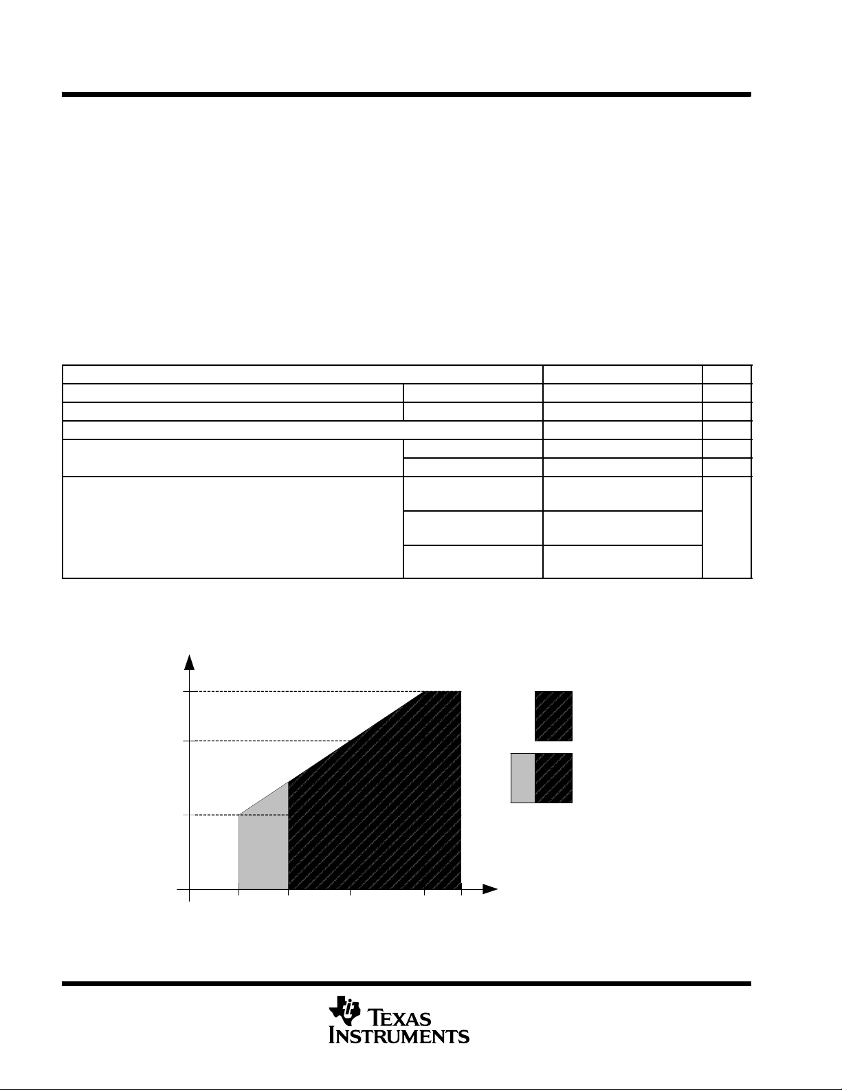
recommended operating conditions
MIN NOM MAX UNITS
Supply voltage during program execution, V
Supply voltage during program/erase flash memory, V
Supply voltage, V
Operatingfree-air temperature range, T
Processor frequency f
NOTES: 1. The MSP430 CPU is clocked directly with MCLK.
SS
(Maximum MCLK frequency)
SYSTEM
Both the high and low phase of MCLK must not exceed the pulse width of the specified maximum frequency.
2. Modules might have a different maximum input clock specification. Refer to the specification of the respective module in this data
sheet.
CC
CC
A
I Version -- 4 0 85 °C
T Version -- 4 0 105 °C
VCC=1.8V,
Duty Cycle = 50% ±10%
VCC=2.7V,
Duty Cycle = 50% ±10%
VCC≥ 3.3 V,
Duty Cycle = 50% ±10%
1.8 3.6 V
2.2 3.6 V
0 V
dc 6
dc 12
dc 16
MHz
16 MHz
12 MHz
6MHz
System Frequency -- MHz
1.8 V 2.2 V 2.7 V 3.3 V 3.6 V
Supply Voltage --V
NOTE: Minimum processor frequency is defined by system clock. Flash program or erase operations require a minimum V
Legend:
Supply voltage range,
during flash memory
programming
Supply voltage range,
during program execution
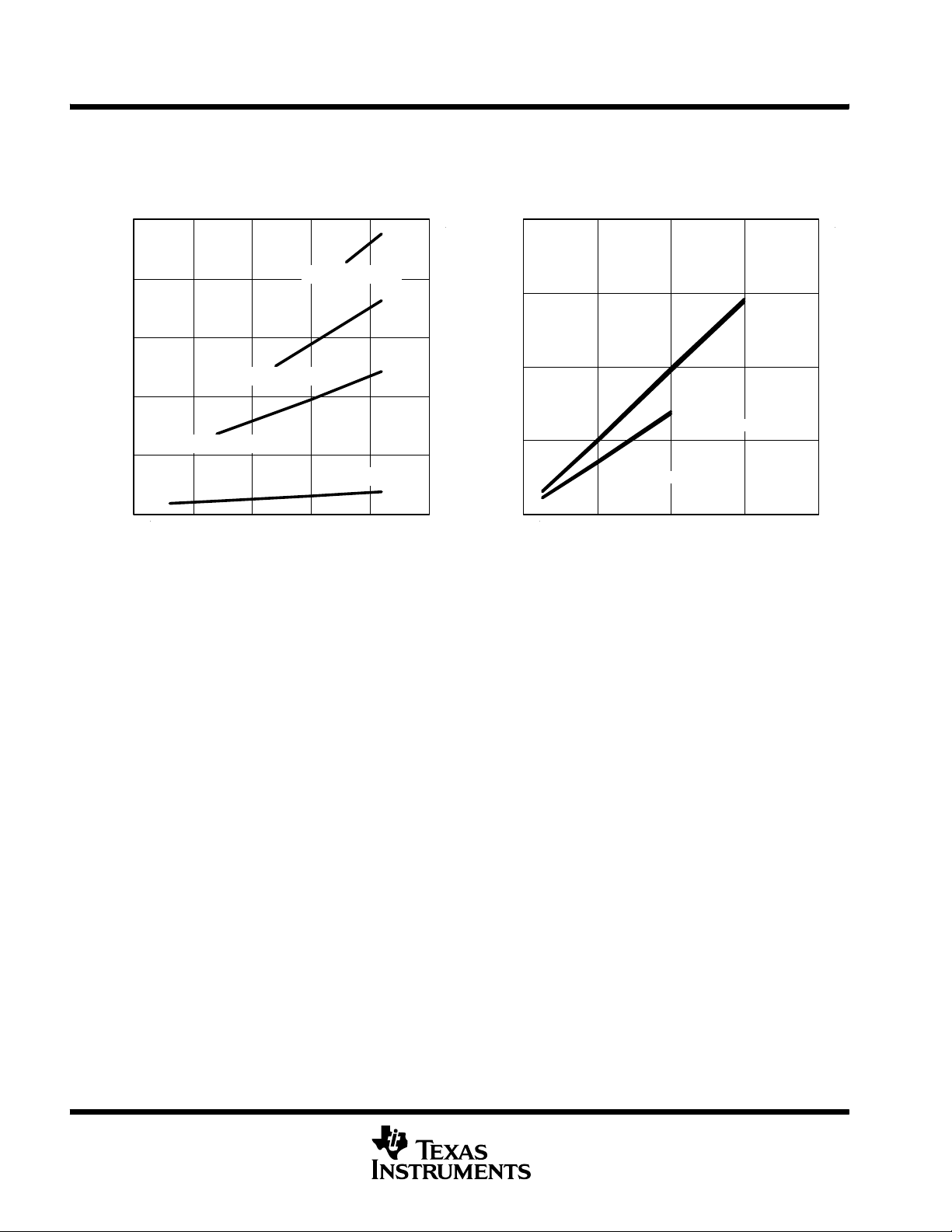
Figure 1. Save Operating Area
20
POST OFFICE BOX 655303 • DALLAS, TEXAS 75265
CC
of 2.2 V.
Page 21
MSP430x20x1, MSP430x20x2, MSP430x20x3
A
(
AM)
Activemode(AM
)
A
A
A
(
AM)
Activemode(AM
)
A
A
f
,
A
(
AM)
f
A
CLK
=32,768Hz/8=4,096Hz
g
Activemode(AM
)
Programexecutesinflas
h
ADIVMxDIVSxDIVAx11,
A
(
AM)
f
f
Activemode(AM
)
Programexecutesinflas
h
A
MIXED SIGNAL MICROCONTROLLER
SLAS491D -- AUGUST 2005 -- REVISED SEPTEMBER 2007
electrical characteristics over recommended ranges of supply voltage and operating free-air temperature (unless otherwise noted)
active mode supply current (into VCC) excluding external current (see Notes 1 and 2)
I
AM, 1MHz
I
AM, 1MHz
I
AM, 4kHz
I
AM,100kHz
PARAMETER TEST CONDITIONS T
ctive mode
current (1MHz)
f
DCO=fMCLK=fSMCLK
f
= 32,768Hz,
ACLK
Program executes in flash,
BCSCTL1 = C
DCOCTL = CALDCO_1MHZ,
=1MHz,
LBC1_1MHZ,
CPUOFF = 0, SCG0 = 0, SCG1 = 0,
OSCOFF = 0
ctive mode
current (1MHz)
f
DCO=fMCLK=fSMCLK
f
= 32,768Hz,
ACLK
Program executes in RAM,
BCSCTL1 = C
DCOCTL = CALDCO_1MHZ,
=1MHz,
LBC1_1MHZ,
CPUOFF = 0, SCG0 = 0, SCG1 = 0,
OSCOFF = 0
ctive mode
current (4kHz)
ctive mode
current (100kHz)
f
MCLK=fSMCLK
=32,768Hz/8=4,096Hz
f
=0Hz,
DCO
Pro
ram executes inflash,
SELMx = 11, SELS = 1,
DIVMx = DIVSx = DIVAx = 11,
CPUOFF = 0, SCG0 = 1, SCG1 = 0,
OSCOFF = 0
f
MCLK=fSMCLK=fDCO(0, 0)
=0Hz,
ACLK
Program executes in
RSELx = 0, DCOx = 0,
CPUOFF = 0, SCG0 = 0, SCG1 = 0,
OSCOFF = 1
=
,
,
-40--85°C 2.2 V 1.2 3
105°C 2.2 V 6
-40--85°C 3V 1.6 4
105°C 3V 7
lash,
≈ 100kHz,
,
-40--85°C 2.2 V 37 50
105°C 2.2 V 60
-40--85°C 3V 40 55
105°C 3V 65
A
VCC MIN TYP MAX UNIT
2.2 V 220 270
μ
3V 300 370
2.2 V 190
μ
3V 260
μ
μ
NOTES: 1. All inputs are tied to 0 V or VCC. Outputs do not source or sink any current.
2. The currents are characterized with a Micro Crystal CC4V--T1A SMD crystal with a load capacitance of 9 pF.
The internal and external load capacitance is chosen to closely match the required 9pF.
POST OFFICE BOX 655303 • DALLAS, TEXAS 75265
21
Page 22
MSP430x20x1, MSP430x20x2, MSP430x20x3
MIXED SIGNAL MICROCONTROLLER
SLAS491D -- AUGUST 2005 -- REVISED SEPTEMBER 2007
electrical characteristics over recommended ranges of supply voltage and operating free-air
temperature (unless otherwise noted) (continued)
typical characteristics -- active mode supply current (into VCC)
5.0
f
=16MHz
=12MHz
DCO
f
DCO
=1MHz
4.0
3.0
f
DCO
2.0
Active Mode Current -- mA
1.0
0.0
1.5 2.0 2.5 3.0 3.5 4.0
f
=8MHz
DCO
VCC-- Supply Voltage -- V
Figure 2. Active mode current vs VCC,TA=25°C
4.0
3.0
2.0
Active Mode Current -- mA
1.0
0.0
0.0 4.0 8.0 12.0 16.0
VCC=3V
TA=85°C
TA=25°C
VCC=2.2V
f
-- DCO Frequency -- MHz
DCO
TA=85°C
TA=25°C
Figure 3. Active mode current vs DCO frequency
22
POST OFFICE BOX 655303 • DALLAS, TEXAS 75265
Page 23
MSP430x20x1, MSP430x20x2, MSP430x20x3
A
A
f
A
CLK
f
ACL
K
=0H
z
A
f
1MH
V
A
A
_
V
V
A
L
(
f
f
f
0MH
f
3(LPM3)curren
t
f
ACL
K
=32,768Hz
V
A
V
A
L
(
)
f
f
f
0MH
f
f
(
VLO)
3curren
t,(LPM3
)
f
ACL
K
frominternalLFoscillator(VLO)
V
A
f
f
f
0MH
f
f
ACL
K
=0H
z
V
/
AseeNote5
MIXED SIGNAL MICROCONTROLLER
SLAS491D -- AUGUST 2005 -- REVISED SEPTEMBER 2007
electrical characteristics over recommended ranges of supply voltage and operating free-air
temperature (unless otherwise noted) (continued)
low power mode supply currents (into VCC) excluding external current (see Notes 1 and 2)
I
LPM0, 1MHz
I
LPM0, 100kHz
I
LPM2
I
LPM3,LFXT1
I
LPM3,VLO
I
LPM4
PARAMETER TEST CONDITIONS T
f
=0MHz,
MCLK
Low-power mode
0 (LPM0) current,
seeNote3
f
SMCLK=fDCO
f
= 32,768 Hz,
ACLK
BCSCTL1 = C
DCOCTL = CALDCO_1MHZ,
=1MHz,
LBC1_1MHZ,
CPUOFF = 1, SCG0 = 0, SCG1 = 0,
OSCOFF = 0
f
=0MHz,
MCLK
Low-power mode
0 (LPM0) current,
seeNote3
f
SMCLK=fDCO(0, 0)
=0Hz,
RSELx = 0, DCOx = 0,
CPUOFF = 1, SCG0 = 0, SCG1 = 0,
≈ 100 kHz,
,
OSCOFF = 1
Low-power mode
2 (LPM2) current,
seeNote4
f
MCLK=fSMCLK
=
DCO
f
= 32,768 Hz,
ACLK
BCSCTL1 = C
DCOCTL = CALDCO_1MHZ,
CPUOFF = 1, SCG0 = 0, SCG1 = 1,
OSCOFF = 0
=0MHz,
z,
LBC1_1MHZ,
-40--85°C
105°C
-40--85°C
105°C
-40°C 0.7 1.2
25°C
ow-power mode
3
LPM3)current,
seeNote4
=
DCO
,
=
MCLK
= 32,768 Hz,
SMCLK
,
=
CPUOFF = 1, SCG0 = 1, SCG1 = 1,
OSCOFF = 0
z,
85°C
105°C 3 6
-40°C 0.9 1.2
25°C
85°C
105°C 3 7
-40°C 0.4 0.7
25°C
ow-power mode
3 current,
LPM3
seeNote4
=
DCO
MCLK
=
SMCLK
=
z,
rom internal LF oscillator
CPUOFF = 1, SCG0 = 1, SCG1 = 1,
OSCOFF = 0
85°C
105°C 2 5
,
,
-40°C 0.5 0.9
25°C
85°C
105°C 2.5 6
-40°C 0.1 0.5
25°C
85°C
105°C 2 4
Low-power mode
4 (LPM4) current,
seeNote5
=
DCO
MCLK
=0Hz,
=
,
SMCLK
=
z,
CPUOFF = 1, SCG0 = 1, SCG1 = 1,
OSCOFF = 1
A
VCC MIN TYP MAX UNIT
2.2 V 65 80
3V 85 100
2.2 V 37 48
3V 41 52
22 29
2.2
31
25 32
3
34
0.7 1.0
1.4 2.3
0.9 1.2
1.6 2.8
0.5 0.7
1.0 1.6
0.6 0.9
1.3 1.8
0.1 0.5
0.8 1.5
2.2
2.2
3
2.2
3
3V
μ
μ
μ
μ
μ
μ
μ
μ
NOTES: 1. All inputs are tied to 0 V or VCC. Outputs do not source or sink any current.
2. The currents are characterized with a Micro Crystal CC4V--T1A SMD crystal with a load capacitance of 9 pF.
The internal and external load capacitance is chosen to closely match the required 9pF.
3. Current for brownout and WDT clocked by SMCLK included.
4. Current for brownout and WDT clocked by ACLK included.
5. Current for brownout included.
POST OFFICE BOX 655303 • DALLAS, TEXAS 75265
23
Page 24
MSP430x20x1, MSP430x20x2, MSP430x20x3
V
IT+
l
t
V
V
I
T
l
t
V
Inputvoltagehysteresis(
V
I
T
V
MIXED SIGNAL MICROCONTROLLER
SLAS491D -- AUGUST 2005 -- REVISED SEPTEMBER 2007
electrical characteristics over recommended ranges of supply voltage and operating free-air
temperature (unless otherwise noted) (continued)
Schmitt-trigger inputs -- Ports P1 and P2
PARAMETER TEST CONDITIONS VCC MIN TYP MAX UNIT
V
IT+
Positive-going input threshold
vo
age
2.2 V 1.00 1.65
3V 1.35 2.25
0.25 0.55 V
0.45 0.75 V
V
IT--
--
Negative-going input threshold
vo
age
2.2 V 0.55 1.20
3V 0.75 1.65
V
hys
R
Pull
C
I
Input voltagehysteresis(V
V
)
IT--
Pull-up/pull-down resistor
Input Capacitance VIN=VSSor V
--
+
For pullup: VIN=VSS;
For pulldown: V
IN=VCC
CC
2.2 V 0.2 1.0
3V 0.3 1.0
20 35 50 kΩ
inputs -- Ports P1 and P2
PARAMETER TEST CONDITIONS VCC MIN TYP MAX UNIT
Port P1, P2: P1.x to P2.x, External
t
(int)
External interrupt timing
trigger pulse width to set interrupt
2.2 V/3 V 20 ns
flag, (see Note 1)
NOTES: 1. An external signal sets the interrupt flag every time the minimum interrupt puls width t
shorter than t
(int)
.
is met. It may be set even with trigger signals
(int)
leakage current -- Ports P1 and P2
PARAMETER TEST CONDITIONS VCC MIN TYP MAX UNIT
I
lkg(Px.x)
NOTES: 1. The leakage current is measured with VSSor VCCapplied to the corresponding pin(s), unless otherwise noted.
High-impedance leakage current see Notes 1 and 2 2.2 V/3 V ±50 nA
2. The leakage of the digital port pins is measured individually. The port pin is selected for input and the pull-up/pull-down resistor is
disabled.
5 pF
CC
CC
24
POST OFFICE BOX 655303 • DALLAS, TEXAS 75265
Page 25
MSP430x20x1, MSP430x20x2, MSP430x20x3
Highleveloutput
V
Lowleveloutpu
t
V
y
f
Portoutputfrequency
P
1.4/SMCLK,CL=20pF,RL=1kOh
m
/
A
f
P
2.0/ACL
K,P
1.4/SMCLK,CL=20pF
MIXED SIGNAL MICROCONTROLLER
SLAS491D -- AUGUST 2005 -- REVISED SEPTEMBER 2007
electrical characteristics over recommended ranges of supply voltage and operating free-air
temperature (unless otherwise noted) (continued)
outputs -- Ports P1 and P2
PARAMETER TEST CONDITIONS VCC MIN TYP MAX UNIT
I
V
OH
High-level output
voltage
I
I
I
I
V
OL
Low-level output
voltage
I
I
I
NOTES: 1. The maximum total current, I
OHmax
voltage drop specified.
2. The maximum total current, I
OHmax
voltage drop specified.
output frequency -- Ports P1 and P2
PARAMETER TEST CONDITIONS VCC MIN TYP MAX UNIT
Px.y
Port_CLK
Port outputfrequenc
(with load)
Clock outputfrequency
NOTES: 1. A resistive divider with 2 times 0.5 kΩ between VCCand VSSis used as load. The output is connected to the center tap of the divider.
2. The output voltage reaches at least 10% and 90% V
P1.4/SMCLK, C
(see Note 1 and 2)
P2.0
(see Note 2)
= --1.5 mA (see Notes 1) 2.2 V VCC--0.25 V
(OHmax)
=--6mA(seeNotes2) 2.2 V VCC-- 0 . 6 V
(OHmax)
= --1.5 mA (see Notes 1) 3V VCC--0.25 V
(OHmax)
=--6mA(seeNotes2) 3V VCC-- 0 . 6 V
(OHmax)
= 1.5 mA (see Notes 1) 2.2 V V
(OLmax)
=6mA(seeNotes2) 2.2 V V
(OLmax)
= 1.5 mA (see Notes 1) 3V V
(OLmax)
=6mA(seeNotes2) 3V V
(OLmax)
and I
and I
, for all outputs combined, should not exceed ±12 mA to hold the maximum
OLmax
, for all outputs combined, should not exceed ±48 mA to hold the maximum
OLmax
=20pF, R
=1kOhm
2.2 V 10 MHz
SS
SS
SS
SS
3V 12 MHz
CLK, P1.4/SMCLK, C
=20pF
2.2 V 12 MHz
3V 16 MHz
at the specified toggle frequency.
CC
CC
CC
CC
CC
VSS+0.25
VSS+0.6
VSS+0.25
VSS+0.6
POST OFFICE BOX 655303 • DALLAS, TEXAS 75265
25
Page 26
MSP430x20x1, MSP430x20x2, MSP430x20x3
A
A
MIXED SIGNAL MICROCONTROLLER
SLAS491D -- AUGUST 2005 -- REVISED SEPTEMBER 2007
electrical characteristics over recommended ranges of supply voltage and operating free-air
temperature (unless otherwise noted) (continued)
typical characteristics -- outputs
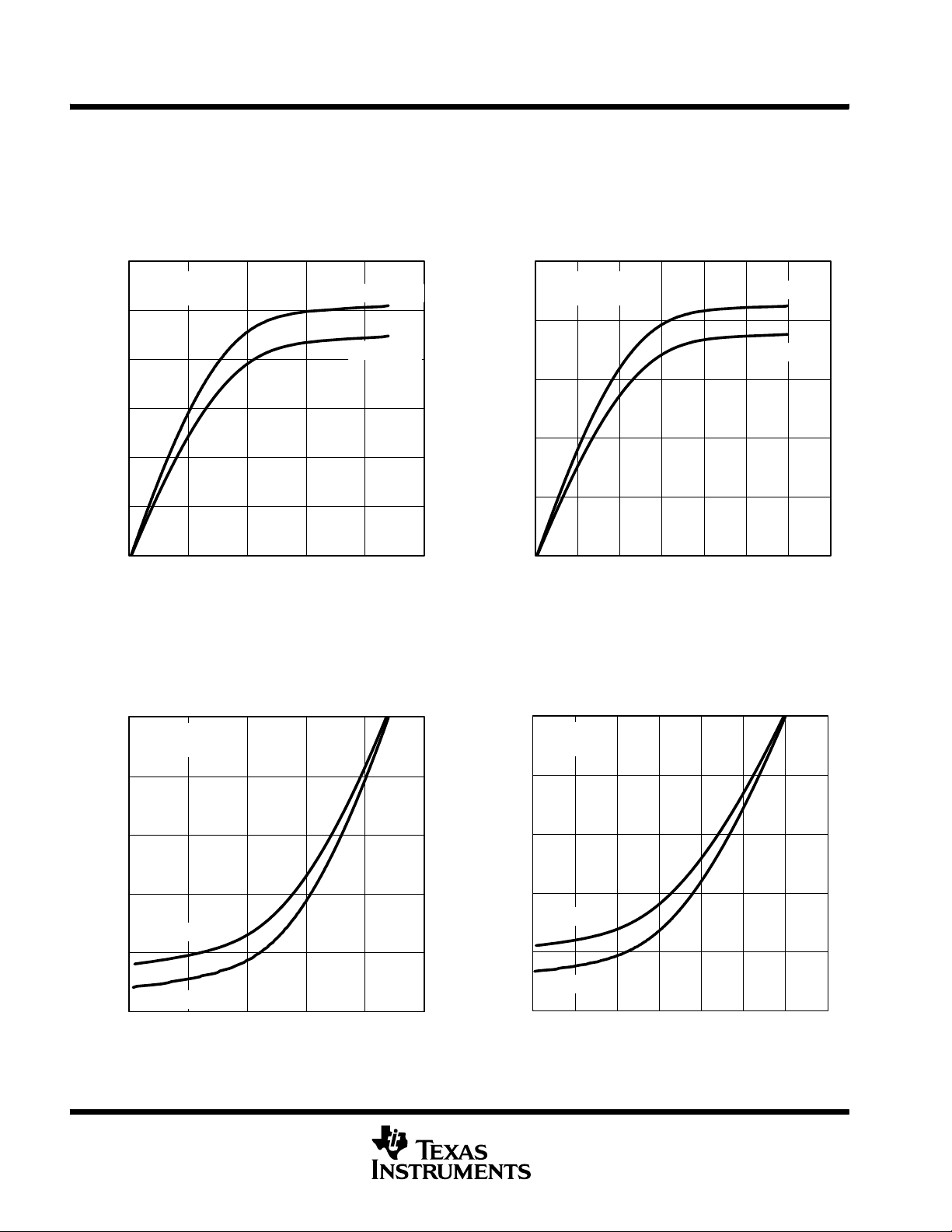
TYPICAL LOW-LEVEL OUTPUT CURRENT
vs
LOW-LEVEL OUTPUT VOLTAGE
30.0
VCC=2.2V
P1.7
5.0
0.0
0.0 0.5 1.0 1.5 2.0 2.5
VOL-- Low-Level Output Voltage -- V
I -- Typical Low-Level Output Current -- m
25.0
20.0
15.0
10.0
OL
Figure 4
TA=25°C
TA=85°C
TYPICAL LOW-LEVEL OUTPUT CURRENT
vs
LOW-LEVEL OUTPUT VOLTAGE
50.0
VCC=3V
P1.7
40.0
30.0
20.0
10.0
OL
I -- Typical Low-Level Output Current -- mA
0.0
0.0 0.5 1.0 1.5 2.0 2.5 3.0 3.5
VOL-- Low-Level Output Voltage -- V
Figure 5
TA=25°C
TA=85°C
TYPICAL HIGH-LEVEL OUTPUT CURRENT
HIGH-LEVEL OUTPUT VOLTAGE
0.0
VCC=2.2V
P1.7
-- 5 . 0
--10.0
--15.0
TA=85°C
--20.0
OH
I -- Typical High-Level Output Current -- m
--25.0
TA=25°C
0.0 0.5 1.0 1.5 2.0 2.5
VOH-- High-Level Output Voltage -- V
Figure 6
NOTE: One output loaded at a time.
vs
TYPICAL HIGH-LEVEL OUTPUT CURRENT
vs
HIGH-LEVEL OUTPUT VOLTAGE
0.0
VCC=3V
P1.7
--10.0
--20.0
--30.0
TA=85°C
--40.0
OH
I -- Typical High-Level Output Current -- mA
--50.0
TA=25°C
0.0 0.5 1.0 1.5 2.0 2.5 3.0 3.5
VOH-- High-Level Output Voltage -- V
Figure 7
26
POST OFFICE BOX 655303 • DALLAS, TEXAS 75265
Page 27
MSP430x20x1, MSP430x20x2, MSP430x20x3
MIXED SIGNAL MICROCONTROLLER
SLAS491D -- AUGUST 2005 -- REVISED SEPTEMBER 2007
electrical characteristics over recommended ranges of supply voltage and operating free-air
temperature (unless otherwise noted) (continued)
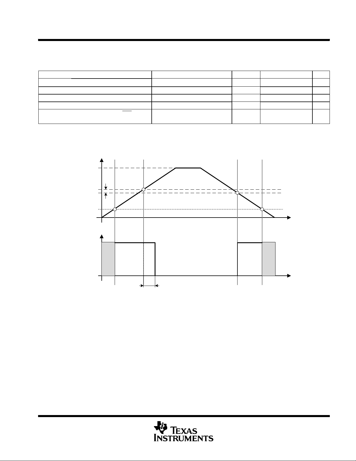
POR/brownout reset (BOR) (see Notes 1 and 2)
PARAMETER TEST CONDITIONS VCC MIN TYP MAX UNIT
V
CC(start)
V
(B_IT--)
V
hys(B_IT--)
t
d(BOR)
t
(reset)
NOTES: 1. The current consumption of the brownout module i s already included in the ICCcurrent consumption data. The voltage level V
(see Figure 8) dVCC/dt ≤ 3V/s 0.7 × V
(B_IT--)
(see Figure 8 through Figure 10) dVCC/dt ≤ 3V/s 1.71 V
(see Figure 8) dVCC/dt ≤ 3V/s 70 130 210 mV
(see Figure 8) 2000 μs
Pulse length needed at RST/NMI pin
to accepted reset internally
+V
hys(B_IT--)
is ≤ 1.8V.
2. During power up, the CPU begins code execution following a period of t
DCO settings must not be changed until V
CC
≥ V
CC(min)
, where V
CC(min)
d(BOR)
is the minimum supply voltage for the desired
2.2 V/3 V 2 μs
after VCC=V
(B_IT--)+Vhys(B_IT--)
operating frequency.
V
CC
V
hys(B_IT--)
V
(B_IT--)
. The default
V
CC(start)
V
(B_IT--)
1
0
t
d(BOR)
Figure 8. POR/Brownout Reset (BOR) vs Supply Voltage
POST OFFICE BOX 655303 • DALLAS, TEXAS 75265
27
Page 28

MSP430x20x1, MSP430x20x2, MSP430x20x3
MIXED SIGNAL MICROCONTROLLER
SLAS491D -- AUGUST 2005 -- REVISED SEPTEMBER 2007
electrical characteristics over recommended ranges of supply voltage and operating free-air
temperature (unless otherwise noted) (continued)
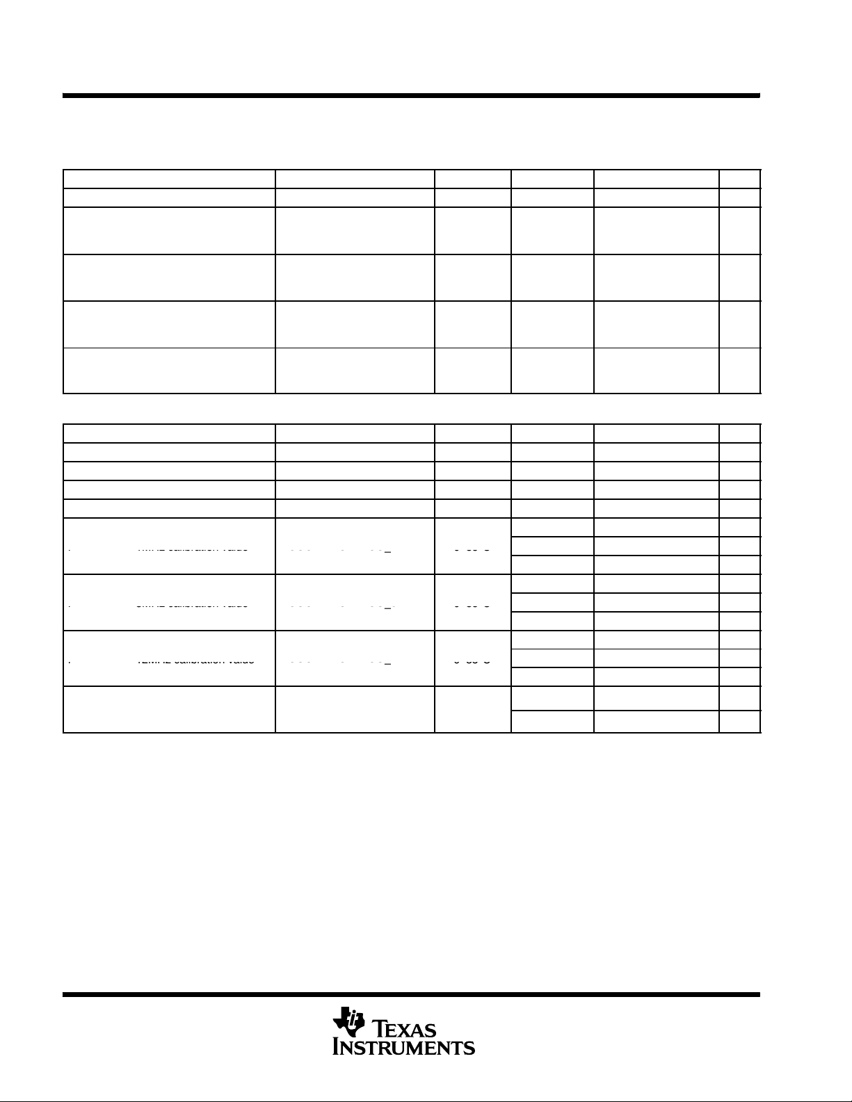
typical characteristics -- POR/brownout reset (BOR)
V
2
1.5
-- V
1
=3V
V
CC
Typical Conditions
CC
3V
t
pw
CC(drop)
V
0.5
0
0.001 1 1000
tpw-- Pulse Width -- μs
Figure 9. V
2
V
Typical Conditions
1.5
-- V
1
CC(drop)
V
0.5
0
0.001 1 1000
Figure 10. V
CC
CC(drop)
=3V
t
CC(drop)
Level With a Square Voltage Drop to Generate a POR/Brownout Signal
-- Pulse Width -- μs
pw
Level With a Triangle Voltage Drop to Generate a POR/Brownout Signal
V
V
CC(drop)
CC(drop)
V
CC
3V
1ns 1ns
tpw-- Pulse Width -- μs
t
pw
tf=t
r
t
f
tpw-- Pulse Width -- μs
t
r
28
POST OFFICE BOX 655303 • DALLAS, TEXAS 75265
Page 29

MSP430x20x1, MSP430x20x2, MSP430x20x3
VccSupplyvoltagerange
MIXED SIGNAL MICROCONTROLLER
SLAS491D -- AUGUST 2005 -- REVISED SEPTEMBER 2007
electrical characteristics over recommended ranges of supply voltage and operating free-air
temperature (unless otherwise noted) (continued)
main DCO characteristics
D All ranges selected by RSELx overlap with RSELx + 1: RSELx = 0 overlaps RSELx = 1, ... RSELx = 14
overlaps RSELx = 15.
D DCO control bits DCOx have a step size as defined by parameter S
D Modulation control bits MODx select how often f
cycles. The frequency f
to:
DCO(RSEL,DCO)
is used for the remaining cycles. The frequency is an average equal
DCO(RSEL,DCO+1)
is used within the period of 32 DCOCLK
DCO
.
f
average
=
MOD × f
32 × f
DCO(RSEL,DCO)
DCO(RSEL,DCO)
× f
DCO(RSEL,DCO+1)
+(32−MOD) × f
DCO(RSEL,DCO+1)
DCO frequency
PARAMETER TEST CONDITIONS VCC MIN TYP MAX UNIT
RSELx < 14 1.8 3.6 V
Vcc Supply voltage range
f
DCO(0,0)
f
DCO(0,3)
f
DCO(1,3)
f
DCO(2,3)
f
DCO(3,3)
f
DCO(4,3)
f
DCO(5,3)
f
DCO(6,3)
f
DCO(7,3)
f
DCO(8,3)
f
DCO(9,3)
f
DCO(10,3)
f
DCO(11,3)
f
DCO(12,3)
f
DCO(13,3)
f
DCO(14,3)
f
DCO(15,3)
f
DCO(15,7)
S
RSEL
S
DCO
Duty Cycle Measured at P1.4/SMCLK 2.2 V/3 V 40 50 60 %
DCO frequency (0, 0) RSELx = 0, DCOx = 0, MODx = 0 2.2 V/3 V 0.06 0.14 MHz
DCO frequency (0, 3) RSELx = 0, DCOx = 3, MODx = 0 2.2 V/3 V 0.07 0.17 MHz
DCO frequency (1, 3) RSELx = 1, DCOx = 3, MODx = 0 2.2 V/3 V 0.10 0.20 MHz
DCO frequency (2, 3) RSELx = 2, DCOx = 3, MODx = 0 2.2 V/3 V 0.14 0.28 MHz
DCO frequency (3, 3) RSELx = 3, DCOx = 3, MODx = 0 2.2 V/3 V 0.20 0.40 MHz
DCO frequency (4, 3) RSELx = 4, DCOx = 3, MODx = 0 2.2 V/3 V 0.28 0.54 MHz
DCO frequency (5, 3) RSELx = 5, DCOx = 3, MODx = 0 2.2 V/3 V 0.39 0.77 MHz
DCO frequency (6, 3) RSELx = 6, DCOx = 3, MODx = 0 2.2 V/3 V 0.54 1.06 MHz
DCO frequency (7, 3) RSELx = 7, DCOx = 3, MODx = 0 2.2 V/3 V 0.80 1.50 MHz
DCO frequency (8, 3) RSELx = 8, DCOx = 3, MODx = 0 2.2 V/3 V 1.10 2.10 MHz
DCO frequency (9, 3) RSELx = 9, DCOx = 3, MODx = 0 2.2 V/3 V 1.60 3.00 MHz
DCO frequency (10, 3) RSELx = 10, DCOx = 3, MODx = 0 2.2 V/3 V 2.50 4.30 MHz
DCO frequency (11, 3) RSELx = 11, DCOx = 3, MODx = 0 2.2 V/3 V 3.00 5.50 MHz
DCO frequency (12, 3) RSELx = 12, DCOx = 3, MODx = 0 2.2 V/3 V 4.30 7.30 MHz
DCO frequency (13, 3) RSELx = 13, DCOx = 3, MODx = 0 2.2 V/3 V 6.00 9.60 MHz
DCO frequency (14, 3) RSELx = 14, DCOx = 3, MODx = 0 2.2 V/3 V 8.60 13.9 MHz
DCO frequency (15, 3) RSELx = 15, DCOx = 3, MODx = 0 3V 12.0 18.5 MHz
DCO frequency (15, 7) RSELx = 15, DCOx = 7, MODx = 0 3V 16.0 26.0 MHz
Frequency step between
range RSEL and RSEL+1
Frequency step between
tap DCO and DCO+1
RSELx = 14
RSELx = 15 3.0 3.6 V
S
RSEL=fDCO(RSEL+1,DCO)/fDCO(RSEL,DCO)
S
DCO=fDCO(RSEL,DCO+1)/fDCO(RSEL,DCO)
2.2 V/3 V 1.55
2.2 V/3 V 1.05 1.08 1.12
2.2 3.6 V
ratio
POST OFFICE BOX 655303 • DALLAS, TEXAS 75265
29
Page 30
MSP430x20x1, MSP430x20x2, MSP430x20x3
)
BCSCTL1=CALBC1_1MHZ
f
CAL(1MHz)
1MHzcalibrationvalueDCOCTLCALDCO_1MHZ
085
C
)
BCSCTL1=CALBC1_8MHZ
f
CAL(8MHz)
8MHzcalibrationvalueDCOCTLCALDCO_8MHZ
085
C
)
BCSCTL1=CALBC1_12MH
Z
f
CAL(12MHz
)
12MHzcalibrationvalueDCOCTLCALDCO_12MHZ
085
C
f
MIXED SIGNAL MICROCONTROLLER
SLAS491D -- AUGUST 2005 -- REVISED SEPTEMBER 2007
electrical characteristics over recommended ranges of supply voltage and operating free-air
temperature (unless otherwise noted) (continued)
calibrated DCO frequencies -- tolerance at calibration
PARAMETER TEST CONDITIONS T
A
Frequency tolerance at calibration 25°C 3V -- 1 ±0.2 +1 %
BCSCTL1= CALBC1_1MHZ
f
CAL(1MHz)
1MHz calibration value
DCOCTL = CALDCO_1MHZ
25°C 3V 0.990 1 1.010 MHz
Gating time: 5ms
BCSCTL1= CALBC1_8MHZ
f
CAL(8MHz)
8MHz calibration value
DCOCTL = CALDCO_8MHZ
25°C 3V 7.920 8 8.080 MHz
Gating time: 5ms
BCSCTL1= CALBC1_12MHZ
f
CAL(12MHz)
12MHz calibration value
DCOCTL = CALDCO_12MHZ
25°C 3V 11.88 12 12.12 MHz
Gating time: 5ms
BCSCTL1= CALBC1_16MHZ
f
CAL(16MHz)
16MHz calibration value
DCOCTL = CALDCO_16MHZ
25°C 3V 15.84 16 16.16 MHz
Gating time: 2ms
calibrated DCO frequencies -- tolerance over temperature 0°C--+85°C
PARAMETER TEST CONDITIONS T
1 MHz tolerance over temperature 0--85°C 3.0 V -- 2 . 5 ±0.5 +2.5 %
8 MHz tolerance over temperature 0--85°C 3.0 V -- 2 . 5 ±1.0 +2.5 %
12 MHz tolerance over temperature 0--85°C 3.0 V -- 2 . 5 ±1.0 +2.5 %
16 MHz tolerance over temperature 0--85°C 3.0 V -- 3 . 0 ±2.0 +3.0 %
=
f
CAL(1MHz
1MHz calibration value
DCOCTL = CALDCO_1MHZ
Gating time: 5ms
=
f
CAL(8MHz
8MHz calibration value
DCOCTL = CALDCO_8MHZ
Gating time: 5ms
=
f
CAL(12MHz
12MHz calibration value
DCOCTL = CALDCO_12MHZ
Gating time: 5ms
BCSCTL1= CALBC1_16MHZ
CAL(16MHz)
16MHz calibration value
DCOCTL = CALDCO_16MHZ
Gating time: 2ms
A
0--85°C
0--85°C
0--85°C
0--85°C
VCC MIN TYP MAX UNIT
VCC MIN TYP MAX UNIT
2.2 V 0.970 1 1.030 MHz
3.0 V 0.975 1 1.025 MHz
3.6 V 0.970 1 1.030 MHz
2.2 V 7.760 8 8.400 MHz
3.0 V 7.800 8 8.200 MHz
3.6 V 7.600 8 8.240 MHz
2.2 V 11.70 12 12.30 MHz
3.0 V 11.70 12 12.30 MHz
3.6 V 11.70 12 12.30 MHz
3.0 V 15.52 16 16.48 MHz
3.6 V 15.00 16 16.48 MHz
30
POST OFFICE BOX 655303 • DALLAS, TEXAS 75265
Page 31

MSP430x20x1, MSP430x20x2, MSP430x20x3
MIXED SIGNAL MICROCONTROLLER
SLAS491D -- AUGUST 2005 -- REVISED SEPTEMBER 2007
electrical characteristics over recommended ranges of supply voltage and operating free-air
temperature (unless otherwise noted) (continued)
calibrated DCO frequencies -- tolerance over supply voltage V
PARAMETER
1MHztoleranceoverV
8MHztoleranceoverV
12 MHz tolerance over V
16 MHz tolerance over V
f
CAL(1MHz)
f
CAL(8MHz)
f
CAL(12MHz)
f
CAL(16MHz)
1MHz calibration value
8MHz calibration value
12MHz calibration value
16MHz calibration value
CC
CC
CC
CC
TEST CONDITIONS T
BCSCTL1= CALBC1_1MHZ
DCOCTL = CALDCO_1MHZ
Gating time: 5ms
BCSCTL1= CALBC1_8MHZ
DCOCTL = CALDCO_8MHZ
Gating time: 5ms
BCSCTL1= CALBC1_12MHZ
DCOCTL = CALDCO_12MHZ
Gating time: 5ms
BCSCTL1= CALBC1_16MHZ
DCOCTL = CALDCO_16MHZ
Gating time: 2ms
calibrated DCO frequencies -- overall tolerance
PARAMETER TEST CONDITIONS T
1MHztoleranceoverall
8MHztoleranceoverall
12 MHz tolerance overall
16 MHz tolerance overall
f
CAL(1MHz)
f
CAL(8MHz)
f
CAL(12MHz)
f
CAL(16MHz)
1MHz calibration value
8MHz calibration value
12MHz calibration value
16MHz calibration value
BCSCTL1= CALBC1_1MHZ
DCOCTL = CALDCO_1MHZ
Gating time: 5ms
BCSCTL1= CALBC1_8MHZ
DCOCTL = CALDCO_8MHZ
Gating time: 5ms
BCSCTL1= CALBC1_12MHZ
DCOCTL = CALDCO_12MHZ
Gating time: 5ms
BCSCTL1= CALBC1_16MHZ
DCOCTL = CALDCO_16MHZ
Gating time: 2ms
I: -40--85°C
T: -40--105°C
I: -40--85°C
T: -40--105°C
I: -40--85°C
T: -40--105°C
I: -40--85°C
T: -40--105°C
I: -40--85°C
T: -40--105°C
I: -40--85°C
T: -40--105°C
I: -40--85°C
T: -40--105°C
I: -40--85°C
T: -40--105°C
CC
A
VCC MIN TYP MAX UNIT
25°C 1.8 V -- 3.6 V -- 3 ±2 +3 %
25°C 1.8 V -- 3.6 V -- 3 ±2 +3 %
25°C 2.2 V -- 3.6 V -- 3 ±2 +3 %
25°C 3.0 V -- 3.6 V -- 3 ±2 +3 %
25°C 1.8 V -- 3.6 V 0.970 1 1.030 MHz
25°C 1.8 V -- 3.6 V 7.760 8 8.240 MHz
25°C 2.2 V -- 3.6 V 11. 6 4 12 12.36 MHz
25°C 3.0 V -- 3.6 V 15.00 16 16.48 MHz
A
VCC MIN TYP MAX UNIT
1.8 V -- 3.6 V -- 5 ±2 +5 %
1.8 V -- 3.6 V -- 5 ±2 +5 %
2.2 V -- 3.6 V -- 5 ±2 +5 %
3.0 V -- 3.6 V -- 6 ±3 +6 %
1.8 V -- 3.6 V 0.950 1 1.050 MHz
1.8 V -- 3.6 V 7.600 8 8.400 MHz
2.2 V -- 3.6 V 11 . 40 12 12.60 MHz
3.0 V -- 3.6 V 15.00 16 17.00 MHz
POST OFFICE BOX 655303 • DALLAS, TEXAS 75265
31
Page 32

MSP430x20x1, MSP430x20x2, MSP430x20x3
MIXED SIGNAL MICROCONTROLLER
SLAS491D -- AUGUST 2005 -- REVISED SEPTEMBER 2007
electrical characteristics over recommended ranges of supply voltage and operating free-air
temperature (unless otherwise noted) (continued)
typical characteristics -- calibrated 1MHz DCO frequency
1.03
1.02
VCC=1.8V
1.01
VCC=2.2V
Frequency -- MHz
1.00
0.99
VCC=3.6V
0.98
VCC=3.0V
0.97
--50.0 --25.0 0.0 25.0 50.0 75.0 100.0
TA-- Temperature -- °C
Figure 11. Calibrated 1 MHz Frequency vs. Temperature
1.03
1.02
1.01
1.00
Frequency -- MHz
0.99
0.98
0.97
1.5 2.0 2.5 3.0 3.5 4.0
V
-- Supply Voltage -- V
CC
Figure 12. Calibrated 1 MHz Frequency vs. V
TA= 105 °C
TA=85°C
TA=25°C
TA=--40°C
CC
32
POST OFFICE BOX 655303 • DALLAS, TEXAS 75265
Page 33

MSP430x20x1, MSP430x20x2, MSP430x20x3
MIXED SIGNAL MICROCONTROLLER
SLAS491D -- AUGUST 2005 -- REVISED SEPTEMBER 2007
electrical characteristics over recommended ranges of supply voltage and operating free-air
temperature (unless otherwise noted) (continued)
wake-up from lower power modes ( LPM3/4)
PARAMETER TEST CONDITIONS VCC MIN TYP MAX UNIT
BCSCTL1= CALBC1_1MHZ
DCOCTL = CALDCO_1MHZ
DCO clock wake-up time from
t
DCO,LPM3/4
t
CPU,LPM3/4
NOTES: 1. The DCO clock wake-up time is measured from the edge of an external wake-up signal (e.g. port interrupt) to the first clock edge
LPM3/4
(see Note 1)
CPU wake-up time from LPM3/4
(see Note 2)
observable externally on a clock pin (MCLK or SMCLK).
2. Parameter applicable only if DCOCLK is used for MCLK.
BCSCTL1= CALBC1_8MHZ
DCOCTL = CALDCO_8MHZ
BCSCTL1= CALBC1_12MHZ
DCOCTL = CALDCO_12MHZ
BCSCTL1= CALBC1_16MHZ
DCOCTL = CALDCO_16MHZ
typical characteristics -- DCO clock wake-up time from LPM3/4
2.2 V/3 V 2
2.2 V/3 V 1.5
2.2 V/3 V 1
3V 1
1/f
+
MCLK
t
Clock,LPM3/4
μs
10.00
RSELx = 0...11
1.00
DCO Wake Time -- us
0.10
0.10 1.00 10.00
DCO Frequency -- MHz
RSELx = 12...15
Figure 13. DCO wake-up time from LPM3 vs DCO frequency
POST OFFICE BOX 655303 • DALLAS, TEXAS 75265
33
Page 34

MSP430x20x1, MSP430x20x2, MSP430x20x3
A
OscillationAllowanceforLF
(seeNote1
)
f
MIXED SIGNAL MICROCONTROLLER
SLAS491D -- AUGUST 2005 -- REVISED SEPTEMBER 2007
electrical characteristics over recommended ranges of supply voltage and operating free-air
temperature (unless otherwise noted) (continued)
crystal oscillator, LFXT1, low frequency modes (see Note 4)
PARAMETER TEST CONDITIONS VCC MIN TYP MAX UNIT
f
LFXT1,LF
f
LFXT1,LF,logic
O
LF
C
L,eff
Duty Cycle LF mode
f
Fault,LF
NOTES: 1. Includes parasitic bond and package capacitance (approximately 2pF per pin).
LFXT1 oscillator crystal
frequency, LF mode 0, 1
LFXT1 oscillator logic level
square wave input frequency,
LF mode
OscillationAllowancefor LF
crystals
Integrated effective Load
Capacitance, LF mode
Osc. fault frequency threshold,
LF mode (see Note 3)
Since the PCB adds additional capacitance it is recommended to verify the correct load by measuring the ACLK frequency. For a
correct setup the effective load capacitance should always match the specification of the used crystal.
2. Measured with logic level input frequency but also applies to operation with crystals.
3. Frequencies below the MIN specification will set the fault flag, frequencies above the MAX specification will not set the fault flag.
Frequencies in between might set the flag.
4. To improve EMI on the LFXT1 oscillator the following guidelines should be observed.
XTS = 0, LFXT1Sx = 0 or 1 1.8 V -- 3.6 V 32,768 Hz
XTS = 0, LFXT1Sx = 3 1.8 V -- 3.6 V 10,000 32,768 50,000 Hz
XTS = 0, LFXT1Sx = 0;
f
LFXT1,LF
C
XTS = 0, LFXT1Sx = 0;
f
LFXT1,LF
C
XTS = 0, XCAPx = 0 1 pF
XTS = 0, XCAPx = 1 5.5 pF
XTS = 0, XCAPx = 2 8.5 pF
XTS = 0, XCAPx = 3 11 pF
XTS = 0, Measured at
P1.4/ACLK,
f
LFXT1,LF
XTS = 0, LFXT1Sx = 3
(see Note 2)
L,eff
L,eff
=6pF
=12pF
= 32,768 kHz,
= 32,768 kHz,
= 32,768 Hz
500 kΩ
200 kΩ
2.2 V/3 V 30 50 70 %
2.2 V/3 V 10 10,000 Hz
-- Keep as short of a trace as possible between the device and the crystal.
-- Design a good ground plane around the oscillator pins.
-- Prevent crosstalk from other clock or data lines into oscillator pins XIN and XOUT.
-- Avoid running PCB traces underneath or adjacent to the XIN and XOUT pins.
-- Use assembly materials and praxis to avoid any parasitic load on the oscillator XIN and XOUT pins.
-- If conformal coating is used, ensure that it does not induce capacitive/resistive leakage between the oscillator pins.
-- Do not route the XOUT line to the JTAG header to support the serial programming adapter as shown in other
documentation. This signal is no longer required for the serial programming adapter.
internal very low power, low frequency oscillator (VLO)
PARAMETER TEST CONDITIONS T
VLO
df
/dT
VLO
df
/dV
VLO
NOTES: 1. Calculated using the box method:
34
VLOfrequency
VLO frequency
temperature drift
VLO frequency supply
CC
voltage drift
I Version: (MAX(--40...85_C) -- MIN(--40...85_C))/MIN(--40...85_C)/(85_C--(--40_C))
T Version: (MAX(--40...105_C) -- MIN(--40...105_C))/MIN(--40...105_C)/(105_C--(--40_C))
2. Calculated using the box method: (MAX(1.8...3.6V) -- MIN(1.8...3.6V))/MIN(1.8...3.6V)/(3.6V -- 1.8V)
(see Note 1)
(see Note 2) 25°C 1.8V -- 3.6V 4 %/V
POST OFFICE BOX 655303 • DALLAS, TEXAS 75265
A
-40--85°C 2.2 V/3 V 4 12 20
105°C 2.2 V/3 V 22
I: -40--85°C
T: -40--105°C
VCC MIN TYP MAX UNIT
kHz
2.2 V/3 V 0.5 %/°C
Page 35

MSP430x20x1, MSP430x20x2, MSP430x20x3
f
_
A
x
f
A
MIXED SIGNAL MICROCONTROLLER
SLAS491D -- AUGUST 2005 -- REVISED SEPTEMBER 2007
electrical characteristics over recommended ranges of supply voltage and operating free-air
temperature (unless otherwise noted) (continued)
Timer_A
PARAMETER TEST CONDITIONS VCC MIN TYP MAX UNIT
Internal: SMCLK, ACLK;
E
ternal: TACLK, INCLK;
Duty Cycle = 50% ±10%
TA
t
TA, cap
Timer
Timer_A, capture timing TA 0, TA1 2.2 V/3 V 20 ns
clockfrequency
USI, Universal Serial Interface (MSP430x20x2, MSP430x20x3 only)
PARAMETER TEST CONDITIONS VCC MIN TYP MAX UNIT
External: SCLK;
Duty Cycle = 50% ±10%;
SPI Slave Mode
USI module in I2C mode
I
(OLmax)
=1.5mA
USI
V
OL,I2C
USI clockfrequency
Low-level output voltage on SDA
and SCL
typical characteristics -- USI low-level output voltage on SDA and SCL (MSP430x20x2, MSP430x20x3 only)
2.2 V 10
3V 16
2.2 V 10
3V 16
2.2 V/3 V V
SS
VSS+0.4 V
MHz
MHz
5.0
VCC=2.2V
4.0
3.0
2.0
1.0
OL
I -- Low-Level Output Current -- m
0.0
0.0 0.2 0.4 0.6 0.8 1.0
VOL-- Low-Level Output Voltage -- V
TA=25°C
TA=85°C
Figure 14. USI Low-Level Output Voltage vs.
Output Current
5.0
VCC=3V
4.0
3.0
2.0
1.0
OL
I -- Low-Level Output Current -- mA
0.0
0.0 0.2 0.4 0.6 0.8 1.0
VOL-- Low-Level Output Voltage -- V
TA=25°C
TA=85°C
Figure 15. USI Low-Level Output Voltage vs.
Output Current
POST OFFICE BOX 655303 • DALLAS, TEXAS 75265
35
Page 36

MSP430x20x1, MSP430x20x2, MSP430x20x3
A
A
/CA
A
V
f
Withoutfilter:CAF=0
Responsetim
e
f
Withfilter:CAF=
1
MIXED SIGNAL MICROCONTROLLER
SLAS491D -- AUGUST 2005 -- REVISED SEPTEMBER 2007
MSP430x20x1 electrical characteristics over recommended ranges of supply voltage and operating free-air temperature (unless otherwise noted)
Comparator_A+ (see Note 1, MSP430x20x1 only)
PARAMETER TEST CONDITIONS VCC MIN TYP MAX UNIT
I
(DD)
CAON=1, CARSEL=0, CAREF=0
CAON=1, CARSEL=0,
I
(Refladder/RefDiode)
CAREF=1/2/3,
no load at P1.0/CA0 and P1.1/CA1
V
(IC)
V
(Ref025)
V
(Ref050)
Common-mode input
voltage
Voltage @ 0.25 VCCnode
V
CC
Voltage @ 0.5VCCnode
V
CC
CAON=1 2.2 V/3 V 0 VCC-- 1 V
PCA0=1, CARSEL=1, CAREF=1,
no load at P1.0/CA0 and P1.1/CA1
PCA0=1, CARSEL=1, CAREF=2,
no load at P1.0/CA0 and P1.1/CA1
PCA0=1, CARSEL=1, CAREF=3,
V
(RefVT)
V
(offset)
V
hys
(see Figure 19 and Figure 20)
no load at P1.0
T
=85°C
0 and P1.1/CA1,
Offset voltage SeeNote2 2.2 V/3 V -- 3 0 30 mV
Input hysteresis CAON=1 2.2 V/3 V 0 0.7 1.4 mV
TA=25°C, Overdrive 10 mV,
Without
ilter: CAF=0
(see Note 3, Figure 16 and
t
(response)
Response time
(low--high and high--low)
Figure 17)
=25°C, Overdrive 10 mV,
T
A
With
ilter: CAF=1
(see Note 3, Figure 16 and
Figure 17)
NOTES: 1. The leakage current for the Comparator_A+ terminals is identical to I
2. The input offset voltage can be cancelled by using the CAEX bit to invert the Comparator_A+ inputs on successive measurements.
The two successive measurements are then summed together.
3. Response time measured at P1.3/CAOUT.
lkg(Px.x)
2.2 V 25 40
3V 45 60
2.2 V 30 50
3V 45 71
2.2 V/3 V 0.23 0.24 0.25
2.2 V/3 V 0.47 0.48 0.5
2.2 V 390 480 540
3V 400 490 550
2.2 V 80 165 300
3V 70 120 240
2.2 V 1.4 1.9 2.8
3V 0.9 1.5 2.2
specification.
μ
μ
m
ns
μs
36
POST OFFICE BOX 655303 • DALLAS, TEXAS 75265
Page 37

MSP430x20x1, MSP430x20x2, MSP430x20x3
MIXED SIGNAL MICROCONTROLLER
SLAS491D -- AUGUST 2005 -- REVISED SEPTEMBER 2007
MSP430x20x1 electrical characteristics over recommended ranges of supply voltage and
operating free-air temperature (unless otherwise noted) (continued)
V
0V
CC
0
1
CAON
CAF
Low Pass Filter
V+
V--
+
_
0
1
τ≈2.0 μs
Figure 16. Block Diagram of Comparator_A+ Module
V
CAOUT
V--
400 mV
V+
Overdrive
t
(response)
Figure 17. Overdrive Definition
To I n t e rnal
Modules
0
1
CAOUT
Set CAIFG
Flag
CASHORT
CA1CA0
1
+
V
IN
--
Comparator_A+
CASHORT = 1
Figure 18. Comparator_A+ Short Resistance Test Condition
I
OUT
=10μA
POST OFFICE BOX 655303 • DALLAS, TEXAS 75265
37
Page 38

MSP430x20x1, MSP430x20x2, MSP430x20x3
(
)
(
)
MIXED SIGNAL MICROCONTROLLER
SLAS491D -- AUGUST 2005 -- REVISED SEPTEMBER 2007
MSP430x20x1 electrical characteristics over recommended ranges of supply voltage and
operating free-air temperature (unless otherwise noted) (continued)
typical characteristics -- Comparator_A+ (MSP430x20x1 only)
650
VCC=3V
600
Typical
550
500
-- Reference Volts --mV
(REFVT)
450
V
400
--45--25--51535557595115
TA-- Free-Air Temperature -- °C
Figure 19. V
vs Temperature, VCC=3V
RefVT
100.00
650
VCC=2.2V
600
Typical
550
500
-- Reference Volts --mV
(REFVT)
450
V
400
--45--25--51535557595115
TA-- Free-Air Temperature -- °C
Figure 20. V
vs Temperature, VCC=2.2V
RefVT
VCC=1.8V
VCC=2.2V
10.00
Short Resistance -- kOhms
1.00
VCC=3.0V
VCC=3.6V
0.0 0.2 0.4 0.6 0.8 1.0
V
-- Normalized Input Voltage -- V/V
IN/VCC
Figure 21. Short Resistance vs VIN/V
CC
38
POST OFFICE BOX 655303 • DALLAS, TEXAS 75265
Page 39

MSP430x20x1, MSP430x20x2, MSP430x20x3
A
p
ply
ADC10supplycurren
t
A
I:4085C
A
f
f
_5V
,
REFON=1
MIXED SIGNAL MICROCONTROLLER
SLAS491D -- AUGUST 2005 -- REVISED SEPTEMBER 2007
MSP430x20x2 electrical characteristics over recommended ranges of supply voltage and
operating free-air temperature (unless otherwise noted) (continued)
10-bit ADC, power supply and input range conditions (see Note 1, MSP430x20x2 only)
V
CC
V
Ax
I
ADC10
PARAMETER TEST CONDITIONS T
Analog supply voltage
range
Analog input voltage range
(see Note 2)
DC10 su
current
(see Note 3)
VSS=0V 2.2 3.6 V
All Ax terminals.
Analog inputs selected in
ADC10AE register.
f
ADC10CLK
=5.0MHz
ADC10ON = 1, REFON = 0
DC10SHT0 = 1,
ADC10SHT1 = 0, ADC10DIV
A
I: -40--85°C
T: -40--105°C
=0
I
REF+
I
REFB,0
I
REFB,1
Reference supply current,
reference bu
er disabled
(see Note 4)
Reference buffer supply
current withADC10SR=0
(see Note 4)
Reference buffer supply
current withADC10SR=1
(see Note 4)
f
ADC10CLK
ADC10ON = 0, REF2_5V = 0,
REFON = 1, REFOUT = 0
f
ADC10CLK
ADC10ON = 0, REF2_5V = 1,
REFON = 1, REFOUT = 0
f
ADC10CLK
ADC10ON = 0,
REFON = 1, REF2
REFOUT = 1,
ADC10SR=0
f
ADC10CLK
ADC10ON = 0,
REFON = 1
REF2_5V = 0,
REFOUT = 1,
=5.0MHz
=5.0MHz
=5.0MHz
=5.0MHz
,
I: -40--85°C
T: -40--105°C
I: -40--85°C
T: -40--105°C
-40--85°C 2.2 V/3 V 1.1 1.4 mA
=0,
105°C 2.2 V/3 V 1.8 mA
-40--85°C 2.2 V/3 V 0.5 0.7 mA
105°C 2.2 V/3 V 0.8 mA
ADC10SR=1
C
I
R
I
Input capacitance
Input MUX ON resistance 0V ≤ VAx≤ V
Only one terminal Ax selected
at a time
CC
I: -40--85°C
T: -40--105°C
I: -40--85°C
T: -40--105°C
NOTES: 1. The leakage current is defined in the leakage current table with Px.x/Ax parameter.
2. The analog input voltage range must be within the selected reference voltage range V
3. The internal reference supply current is not included in current consumption parameter I
4. The internal reference current is supplied via terminal V
. Consumption is independent of the ADC10ON control bit, unless a
CC
conversion is active. The REFON bit enables the built-in reference to settle before starting an A/D conversion.
VCC MIN TYP MAX UNIT
0 V
CC
2.2 V 0.52 1.05
m
3V 0.6 1.2
2.2 V/3 V
mA
0.25 0.4
3V
mA
27 pF
2.2 V/3 V 2000 Ω
to V
R+
for valid conversion results.
R--
.
ADC10
V
POST OFFICE BOX 655303 • DALLAS, TEXAS 75265
39
Page 40

MSP430x20x1, MSP430x20x2, MSP430x20x3
V
C
C,REF
+
l
t
V
A
x
V
V
f
f
REF2_5V=0
Settlingtimeofreferencebuffer
V
REF2_5V=1
MIXED SIGNAL MICROCONTROLLER
SLAS491D -- AUGUST 2005 -- REVISED SEPTEMBER 2007
MSP430x20x2 electrical characteristics over recommended ranges of supply voltage and
operating free-air temperature (unless otherwise noted) (continued)
10-bit ADC, built-in voltage reference (MSP430x20x2 only)
PARAMETER TEST CONDITIONS VCC MIN TYP MAX UNIT
I
≤ 1mA, REF2_5V=0 2.2
V
CC,REF+
V
REF+
I
LD,VREF+
C
VREF+
TC
REF+
t
REFON
t
REFBURST
Positive built-in reference analog
supplyvo
age range
Positive built-in reference voltage
Maximum V
V
load regulation
REF+
V
load regulation response time
REF+
Max. capacitance at pin V
REF+
load current
REF+
(see Note 1)
Temperature coefficient
Settling time of internal reference
voltage (see Note 2)
Settlingtime ofreference bu
er
(see Note 2)
NOTES: 1. The capacitance applied to the internal buffer operational amplifier, if switched to terminal P2.4/TA2/A4/V
must be limited; the reference buffer may become unstable otherwise.
2. The condition is that the error in a conversion started after t
VREF+
I
≤ 0.5mA, REF2_5V=1 2.8
VREF+
I
≤ 1mA, REF2_5V=1 2.9
VREF+
I
VREF+
I
VREF+
≤ I
≤ I
max, REF2_5V = 0 2.2 V/3 V 1.41 1.5 1.59 V
VREF+
max, REF2_5V = 1 3V 2.35 2.5 2.65 V
VREF+
2.2 V ±0.5
I
= 500 μA +/-- 100 μA
VREF+
Analog input voltage V
≈ 0.75 V;
Ax
2.2 V/3 V ±2 LSB
REF2_5V = 0
I
= 500 μA ± 100 μA
VREF+
Analog input voltage V
≈ 1.25 V;
Ax
REF2_5V = 1
I
=
VREF+
100μA→900μA,
≈ 0.5
V
Ax
REF+
Error of conversion
result ≤ 1LSB
I
≤±1mA,
VREF+
REFON = 1, REFOUT = 1
I
= const. with
VREF+
0mA≤ I
I
VREF+
≤ 1mA
VREF+
= 0.5 mA, REF2_5V=0
REFON = 0 → 1
I
=0.5mA,
VREF+
REF2 5
=0,
,
REFON = 1,
REFBURST = 1
=0.5mA,
I
VREF+
REF2 5
=1,
,
REFON = 1,
REFBURST = 1
ADC10SR = 0 3V 400
ADC10SR = 1 3V 2000
2.2 V/3 V 100 pF
2.2 V/3 V ±100 ppm/°C
3.6 V 30
ADC10SR = 0 2.2 V 1
ADC10SR = 1 2.2 V 2.5
ADC10SR = 0 3V 2
ADC10SR = 1 3V 4.5
REFON
or t
is less than ±0.5 LSB.
RefBuf
V
3V ±1
m
3V ±2 LSB
ns
μs
μs
REF+/VeREF+
(REFOUT=1),
40
POST OFFICE BOX 655303 • DALLAS, TEXAS 75265
Page 41

MSP430x20x1, MSP430x20x2, MSP430x20x3
Positiveexternalreferenceinpu
t
MIXED SIGNAL MICROCONTROLLER
SLAS491D -- AUGUST 2005 -- REVISED SEPTEMBER 2007
MSP430x20x2 electrical characteristics over recommended ranges of supply voltage and
operating free-air temperature (unless otherwise noted) (continued)
10-bit ADC, external reference (see Note 1, MSP430x20x2 only)
PARAMETER TEST CONDITIONS VCC MIN TYP MAX UNIT
V
eREF+>VeREF--
V
eREF+
Positive external reference input
voltage range (see Note 2)
SREF1 = 1, SREF0 = 0
V
eREF--
≤ V
eREF+
≤ VCC-- 0.15V
SREF1=1,SREF0=1(seeNote3)
V
eREF--
Negative external reference input
voltage range (see Note 4)
V
eREF+>VeREF--
Differential external reference input
∆V
eREF
I
VeREF+
I
VeREF --
voltage range
∆V
eREF=VeREF+
-- V
eREF--
Static input current into V
Static input current into V
eREF+
eREF--
V
eREF+>VeREF--
0V ≤ V
eREF+
(see Note 5) 1.4 V
≤ VCC,
SREF1 = 1, SREF0 = 0
0V ≤V
≤ VCC-- 0.15V ≤ 3V
eREF+
SREF1=1,SREF0=1(seeNote3)
0V ≤ V
eREF--
≤ V
CC
2.2 V/3 V ±1 μA
2.2 V/3 V 0 μA
2.2 V/3 V ±1 μA
NOTES: 1. The external reference is used during conversion to charge and discharge the capacitance array. The input capacitance, CI,isalso
the dynamic load for an external reference during conversion. The dynamic impedance of the reference supply should follow the
recommendations on analog-source impedance to allow the charge to settle for 10-bit accuracy.
2. The accuracy limits the minimum positive external reference voltage. Lower reference voltage levels may be applied with reduced
accuracy requirements.
3. Under this condition the external reference is internally buffered. The reference buffer is active and requires the reference buffer
supply current I
. The current consumption can be limited to the sample and conversion period with REBURST = 1.
REFB
4. The accuracy limits the maximum negative external reference voltage. Higher reference voltage levels may be applied with reduced
accuracy requirements.
5. The accuracy limits the minimum external differential reference voltage. Lower differential reference voltage levels may be applied
with reduced accuracy requirements.
1.4 V
CC
1.4 3.0 V
0 1.2 V
CC
V
V
POST OFFICE BOX 655303 • DALLAS, TEXAS 75265
41
Page 42

MSP430x20x1, MSP430x20x2, MSP430x20x3
perf
f
f
A
performanceof
MIXED SIGNAL MICROCONTROLLER
SLAS491D -- AUGUST 2005 -- REVISED SEPTEMBER 2007
MSP430x20x2 electrical characteristics over recommended ranges of supply voltage and
operating free-air temperature (unless otherwise noted) (continued)
10-bit ADC, timing parameters (MSP430x20x2 only)
PARAMETER TEST CONDITIONS VCC MIN TYP MAX UNIT
For specified
ADC10CLK
DC10 input clockfrequency
ormance o
ADC10 linearity
parameters
f
ADC10OSC
ADC10 built-in oscillator frequency
ADC10DIVx=0, ADC10SSELx = 0
f
ADC10CLK=fADC10OSC
ADC10 built-in oscillator,
ADC10SSELx = 0
f
t
CONVERT
Conversion time
ADC10CLK=fADC10OSC
f
ADC10CLK
from ACLK, MCLK or
SMCLK: ADC10SSELx ≠ 0
t
ADC10ON
Turn on settling time of the ADC (see Note 1) 100 ns
NOTES: 1. The condition is that the error in a conversion started after t
settled.
ADC10SR = 0 2.2 V/3 V 0.45 6.3
ADC10SR = 1 2.2 V/3 V 0.45 1.5
2.2 V/3 V 3.7 6.3 MHz
2.2 V/3 V 2.06 3.51 μs
ADC10DIV×
1/f
ADC10ON
is less than ±0.5 LSB. The reference and input signal are already
MHz
13×
μs
ADC10CLK
10-bit ADC, linearity parameters (MSP430x20x2 only)
PARAMETER TEST CONDITIONS VCC MIN TYP MAX UNIT
E
I
E
D
E
O
E
G
E
T
Integral linearity error 2.2 V/3 V ±1 LSB
Differential linearity error 2.2 V/3 V ±1 LSB
Offset error
Source impedance RS< 100 Ω, 2.2 V/3 V ±1 LSB
Gain error
Total unadjusted error
2.2 V/3 V ±1.1 ±2 LSB
2.2 V/3 V ±2 ±5 LSB
42
POST OFFICE BOX 655303 • DALLAS, TEXAS 75265
Page 43

MSP430x20x1, MSP430x20x2, MSP430x20x3
p
ply
Temperaturesensorsupply
REFON=0,INCHx=0Ah
A
Sensoroutputvoltage
Currentintodivideratchannel
A
A
A
ADC10ON=1,INCHx=0Bh
V
A
ADC10ON=1,INCHx=0Bh
MIXED SIGNAL MICROCONTROLLER
SLAS491D -- AUGUST 2005 -- REVISED SEPTEMBER 2007
MSP430x20x2 electrical characteristics over recommended ranges of supply voltage and
operating free-air temperature (unless otherwise noted) (continued)
10-bit ADC, temperature sensor and built-in V
PARAMETER TEST CONDITIONS VCC MIN TYP MAX UNIT
I
SENSOR
TC
SENSOR
V
Offset,Sensor
V
Sensor
Temperature sensor su
current (see Note 1)
Sensor offset voltage
Sensor output voltage
(see Note 3)
Sample time required if
t
Sensor(sample)
I
VMID
V
MID
channel 10 is selected (see
Note 4)
Current into divider at channel
11 (see Note 5)
VCCdivider at channel 11
Sample time required if
t
VMID(sample)
channel 11 is selected (see
Note 6)
NOTES: 1. The sensor current I
is high). When REFON = 1, I
sensor input (INCH = 0Ah).
2. The following formula can be used to calculate the temperature sensor output voltage:
V
Sensor,typ
V
Sensor,typ
=TC
=TC
Sensor
Sensor
3. Values are not based on calculations using TC
4. The typical equivalent impedance of the sensor is 51 kΩ. The sample time required includes the sensor-on time t
5. No additional current is needed. The V
6. The on-time t
VMID(on)
is consumed if (ADC10ON = 1 and REFON = 1), or (ADC10ON=1 and INCH=0Ah and sample signal
SENSOR
SENSOR
( 273 + T [°C] ) + V
T[°C] + V
is included in the sampling time t
REFON = 0, INCHx=0Ah,
T
=25_C
A
ADC10ON = 1, INCHx = 0Ah
(see Note 2)
ADC10ON = 1, INCHx = 0Ah
(see Note 2)
Temperature sensor voltage
at T
= 105°C (T Version only)
A
Temperature sensor voltage
at T
=85°C
A
Temperature sensor voltage
at T
=25°C
A
Temperature sensor voltage
at T
=0°C
A
ADC10ON = 1, INCHx = 0Ah,
Error of conversion result ≤ 1LSB
DC10ON = 1, INCHx=0Bh,
DC10ON = 1, INCHx=0Bh,
V
is ≈0.5 x V
MID
DC10ON = 1, INCHx=0Bh,
Error of conversion result ≤ 1LSB
is included in I
Offset,sensor
Sensor(TA
=0°C) [mV]
is used during sampling.
MID
(MSP430x20x2 only)
MID
,
CC
. When REFON = 0, I
REF+
[mV] or
or V
Sensor
Offset,sensor
VMID(sample)
; no additional on time is needed.
2.2 V 40 120
3V 60 160
2.2 V/3 V 3.44 3.55 3.66 mV/°C
2.2 V/3 V 1265 1365 1465 mV
2.2 V/3 V 1195 1295 1395
2.2 V/3 V 985 1085 1185
2.2 V/3 V 895 995 1095
2.2 V/3 V 30 μs
2.2 V NA
3V NA
,
2.2 V 1.06 1.1 1.14
3V 1.46 1.5 1.54
,
2.2 V 1400
3V 1220
applies during conversion of the temperature
SENSOR
but on measurements.
μ
--100 100 mV
mV
μ
ns
SENSOR(on)
.
POST OFFICE BOX 655303 • DALLAS, TEXAS 75265
43
Page 44

MSP430x20x1, MSP430x20x2, MSP430x20x3
f
V
A
A
p
ply
SD16OSR=256
Analogsupplycurrent
f
V
ASD16OS
R=256GA
f
f
Differentialfullscaleinputvoltage
f
V(seeNote1)
Inputimpedanc
e
f
f
f
DifferentialInputimpedanc
e
f
MIXED SIGNAL MICROCONTROLLER
SLAS491D -- AUGUST 2005 -- REVISED SEPTEMBER 2007
MSP430x20x3 electrical characteristics over recommended ranges of supply voltage and operating free-air temperature (unless otherwise noted)
SD16_A, power supply and recommended operating conditions (MSP430x20x3 only)
AV
I
SD16
f
SD16
f
SD16
PARAMETER TEST CONDITIONS T
Analog supply voltage range
CC
nalogsu
including internal reference
SD16 input clock frequency
SD16 input clock frequency
current
AVCC=DVCC=V
CC
AVSS=DVSS=VSS=0V
GAIN: 1,2
SD16LP = 0,
SD16
=1MHz,
GAIN: 4,8,16
=
GAIN: 32
SD16LP = 1,
=0.5MHz,
SD16
=
GAIN: 1
IN: 32
SD16LP = 0
(Low power mode disabled)
SD16LP = 1
(Low power mode enabled)
A
-40--85°C 730 1050
105°C 1170
-40--85°C
105°C
-40--85°C 1160 1700
105°C 1850
-40--85°C 720 1030
105°C
-40--85°C
105°C 1300
VCC MIN TYP MAX UNIT
2.5 3.6 V
3
3
810 1150
1300
1160
810 1150
μ
μ
3V 0.03 1 1.1 MHz
3V 0.03 0.5 MHz
SD16_A, input range (MSP430x20x3 only)
PARAMETER TEST CONDITIONS VCC MIN TYP MAX UNIT
Di
V
ID,FSR
erentialfull scale input voltage
range (see Note 1)
Differential input voltage range
V
ID
Z
I
Z
ID
V
I
V
IC
or specified performance
Input impedance
(one input pin to AVSS)
Di
erential Input impedance
(IN+ to IN--)
Absolute input voltage range
Common-mode input voltage
range
NOTES: 1. The analog input range depends on the reference voltage applied to V
is defined by V
V
or V
FSR+
FSR--
FSR+
.
=+(V
/2)/GAIN and V
REF
Bipolar Mode, SD16UNI = 0
Unipolar Mode, SD16UNI = 1
SD16GAINx=1 ±500
SD16GAINx=2 ±250
SD16REFON=1
SD16GAINx=4 ±125
SD16GAINx=8 ±62
SD16GAINx=16 ±31
SD16GAINx=32 ±15
SD16
SD16
FSR--
=1MHz
=1MHz
=--(V
SD16GAINx=1 3V 200
SD16GAINx=32 3V 75
SD16GAINx=1 3V 300 400
SD16GAINx=32 3V 100 150
/2)/GAIN. The analog input range should not exceed 80% of
REF
REF
.IfV
-- ( V
/2)/
REF
GAIN
0
AV
SS
-0.1V
AV
SS
-0.1V
is sourced externally, the full-scale range
REF
+(V
+(V
REF
GAIN
REF
GAIN
AV
AV
/2)/
/2)/
CC
CC
mV
mV
m
kΩ
kΩ
V
V
44
POST OFFICE BOX 655303 • DALLAS, TEXAS 75265
Page 45
MSP430x20x1, MSP430x20x2, MSP430x20x3
V
SignaltoNoise+DistortionRatio
V
SignaltoNoise+DistortionRatio
MIXED SIGNAL MICROCONTROLLER
SLAS491D -- AUGUST 2005 -- REVISED SEPTEMBER 2007
MSP430x20x3 electrical characteristics over recommended ranges of supply voltage and
operating free-air temperature (unless otherwise noted) (continued)
SD16_A, SINAD performance (f
PARAMETER TEST CONDITIONS
SINAD
1024
Signal-to-Noise + Distortion Ratio
(OSR = 1024)
SD16_A, SINAD performance (f
PARAMETER TEST CONDITIONS
SINAD
256
Signal-to-Noise + Distortion Ratio
(OSR = 256)
= 1MHz, SD16OSRx = 1024, SD16REFON = 1, MSP430x20x3 only)
SD16
CC
PW, or N RSA
MIN TYP MIN TYP
SD16GAINx = 1,
Signal Amplitude: V
Signal Frequency: f
= 500mV,
IN
= 100Hz
IN
3V 84 85 86 87
SD16GAINx = 2,
Signal Amplitude: V
Signal Frequency: f
= 250mV,
IN
= 100Hz
IN
3V 82 83 82 83
SD16GAINx = 4,
Signal Amplitude: V
Signal Frequency: f
= 125mV,
IN
= 100Hz
IN
3V 78 79 78 79
SD16GAINx = 8,
Signal Amplitude: V
Signal Frequency: f
= 62mV,
IN
= 100Hz
IN
3V 73 74 73 74
SD16GAINx = 16,
Signal Amplitude: V
Signal Frequency: f
= 31mV,
IN
= 100Hz
IN
3V 68 69 68 69
SD16GAINx = 32,
Signal Amplitude: V
Signal Frequency: f
= 1MHz, SD16OSRx = 256, SD16REFON = 1, MSP430x20x3 only)
SD16
= 15mV,
IN
= 100Hz
IN
3V 62 63 62 63
CC
PW, or N RSA
MIN TYP MIN TYP
SD16GAINx = 1,
Signal Amplitude: V
Signal Frequency: f
= 500mV,
IN
= 100Hz
IN
3V 80 81 82 83
SD16GAINx = 2,
Signal Amplitude: V
Signal Frequency: f
= 250mV,
IN
= 100Hz
IN
3V 74 75 76 77
SD16GAINx = 4,
Signal Amplitude: V
Signal Frequency: f
= 125mV,
IN
= 100Hz
IN
3V 69 70 71 72
SD16GAINx = 8,
Signal Amplitude: V
Signal Frequency: f
= 62mV,
IN
= 100Hz
IN
3V 63 64 67 68
SD16GAINx = 16,
Signal Amplitude: V
Signal Frequency: f
= 31mV,
IN
= 100Hz
IN
3V 58 59 63 64
SD16GAINx = 32,
Signal Amplitude: V
Signal Frequency: f
= 15mV,
IN
= 100Hz
IN
3V 52 53 57 58
UNIT
dB
UNIT
dB
POST OFFICE BOX 655303 • DALLAS, TEXAS 75265
45
Page 46

MSP430x20x1, MSP430x20x2, MSP430x20x3
f
f
f
f
p
p
/
OffsetErrorTemperatur
e
ppm
MIXED SIGNAL MICROCONTROLLER
SLAS491D -- AUGUST 2005 -- REVISED SEPTEMBER 2007
MSP430x20x3 electrical characteristics over recommended ranges of supply voltage and
operating free-air temperature (unless otherwise noted) (continued)
typical characteristics -- SD16_A SINAD performance over OSR (MSP430x20x3 only)
90.0
85.0
80.0
75.0
70.0
SINAD -- dB
65.0
60.0
55.0
10.00 100.00 1000.00
Figure 22. SINAD performance over OSR, f
SD16_A, performance (f
PARAMETER TEST CONDITIONS VCC MIN TYP MAX UNIT
G
dG/dT Gain Temperature Drift SD16GAINx = 1 (see Note 1) 3V 15 ppm/_C
E
OS
dE
dT
OS
CMRR Common-Mode Rejection Ratio
DC PSR DC Power Supply Rejection
AC PSRR AC Power Supply Rejection Ratio
NOTES: 1. Calculated using the box method: (MAX(--40...85_C) -- MIN(--40...85_C)) / MIN(--40...85_C) / (85_C--(--40_C))
Nominal Gain
O
set Error
O
set Error Temperature
Coefficient
2. Calculated using the ADC output code and the box method:
(MAX-code(2.5...3.6V) -- MIN-code(2.5...3.6V)) / MIN-code(2.5...3.6V) / (3.6V -- 2.5V)
= 1MHz, SD16OSRx = 256, SD16REFON = 1, MSP430x20x3 only)
SD16
RSA
PW, or N
OSR
= 1MHz, SD16REFON = 1, SD16GAINx = 1
SD16
SD16GAINx = 1 3V 0.97 1.00 1.02
SD16GAINx = 2 3V 1.90 1.96 2.02
SD16GAINx = 4 3V 3.76 3.86 3.96
SD16GAINx = 8
SD16GAINx = 16 3V 14.56 15.04 15.52
SD16GAINx = 32 3V 27.20 28.35 29.76
SD16GAINx = 1 3V ±0.2
SD16GAINx = 32
SD16GAINx = 1 3V ±4 ±20
SD16GAINx = 32
SD16GAINx = 1,
Common-mode input signal:
V
= 500 mV, fIN= 50 Hz, 100 Hz
ID
SD16GAINx = 32,
Common-mode input signal:
V
=16mV,fIN= 50 Hz, 100 Hz
ID
SD16GAINx = 1; VIN= 500mV
V
= 2.5V - 3.6V (see Note 2)
CC
SD16GAINx = 1
V
=3.0V±100mV, fIN=50Hz
CC
3V 7.36 7.62 7.84
3V ±1.5
3V ±20 ±100
3V >90
3V >75
2.5V--3.6V 0.35 %/V
3V >80 dB
%FSR
FSR/_C
dB
m
46
POST OFFICE BOX 655303 • DALLAS, TEXAS 75265
Page 47

MSP430x20x1, MSP430x20x2, MSP430x20x3
SD16REFON=1
A
p
ply
ReferenceSupply+Reference
SD16REFON=1
A
MIXED SIGNAL MICROCONTROLLER
SLAS491D -- AUGUST 2005 -- REVISED SEPTEMBER 2007
MSP430x20x3 electrical characteristics over recommended ranges of supply voltage and operating free-air temperature (unless otherwise noted) (continued)
SD16_A, built-in voltage reference (MSP430x20x3 only)
PARAMETER TEST CONDITIONS T
V
I
REF
REF
Internal reference voltage
Reference supply current
TC Temperature coefficient
C
REF
I
LOAD
t
ON
DC PSR
V
load capacitance
REF
V
maximum load current
REF(I)
Turn on time
DC Power Supply Rejection
∆V
/∆V
REF
CC
NOTES: 1. There is no capacitance required on V
voltage noise.
A
SD16REFON = 1,
SD16VMIDON = 0
SD16REFON = 1,
SD16VMIDON = 0
-40--85°C 3V 190 280
,
105°C 3V 295
SD16REFON = 1,
SD16VMIDON = 0
SD16REFON = 1,
SD16VMIDON = 0
(see Note 1)
SD16REFON = 1;
SD16VMIDON = 0
SD16REFON = 0 → 1;
SD16VMIDON = 0;
C
= 100nF
REF
SD16REFON = 1;
SD16VMIDON = 0;
V
= 2.5V - 3.6V
CC
. However, a capacitance of at least 100nF is recommended to reduce any reference
REF
VCC MIN TYP MAX UNIT
3V 1.14 1.20 1.26 V
μ
3V 18 50 ppm/K
100 nF
3V ±200 nA
3V 5 ms
2.5V--3.6V 100 uV/V
SD16_A, reference output buffer (MSP430x20x3 only)
PARAMETER TEST CONDITIONS T
V
REF,BUF
I
REF,BUF
C
REF(O)
I
LOAD,Max
Reference buffer output voltage
Reference Su
+Reference SD16REFON = 1,
output buffer quiescent current
Required load capacitance
on V
REF
Maximum load current on V
REF
Maximum voltage variation vs. load current |I
SD16REFON = 1,
SD16VMIDON = 1
SD16VMIDON = 1
SD16REFON = 1,
SD16VMIDON = 1
SD16REFON = 1,
SD16VMIDON = 1
|=0to1mA 3V -- 1 5 +15 mV
LOAD
SD16REFON = 0 → 1;
t
ON
Turn on time
SD16VMIDON = 1;
C
= 470nF
REF
SD16_A, external reference input (MSP430x20x3 only)
PARAMETER TEST CONDITIONS VCC MIN TYP MAX UNIT
V
REF(I)
I
REF(I)
Input voltage range SD16REFON = 0 3V 1.0 1.25 1.5 V
Input current SD16REFON = 0 3V 50 nA
A
VCC MIN TYP MAX UNIT
3V 1.2 V
--40--85°C 3V 385 600
,
105°C 3V 660
470 nF
3V ±1 mA
3V 100 μs
μ
POST OFFICE BOX 655303 • DALLAS, TEXAS 75265
47
Page 48

MSP430x20x1, MSP430x20x2, MSP430x20x3
(seeNote2
)
MIXED SIGNAL MICROCONTROLLER
SLAS491D -- AUGUST 2005 -- REVISED SEPTEMBER 2007
MSP430x20x3 electrical characteristics over recommended ranges of supply voltage and
operating free-air temperature (unless otherwise noted) (continued)
SD16_A, temperature sensor (MSP430x20x3 only)
PARAMETER TEST CONDITIONS VCC MIN TYP MAX UNIT
TC
Sensor
V
Offset,Sensor
V
Sensor
NOTES: 1. The following formula can be used to calculate the temperature sensor output voltage:
Sensor temperature coefficient 1.18 1.32 1.46 mV/K
Sensor offset voltage --100 100 mV
Temperature sensor voltage
at T
A
Sensor output voltage
(see Note 2)
Temperature sensor voltage
at T
A
Temperature sensor voltage
at T
A
V
Sensor,typ
V
Sensor,typ
=TC
=TC
( 273 + T [°C] ) + V
Sensor
T[°C] + V
Sensor
Sensor(TA
Offset,sensor
=0°C) [mV]
2. Values are not based on calculations using TC
=85°C
=25°C
=0°C
Sensor
[mV] or
or V
Offset,sensor
but on measurements.
3V 435 475 515
3V 355 395 435
3V 320 360 400
mV
48
POST OFFICE BOX 655303 • DALLAS, TEXAS 75265
Page 49

MSP430x20x1, MSP430x20x2, MSP430x20x3
MIXED SIGNAL MICROCONTROLLER
SLAS491D -- AUGUST 2005 -- REVISED SEPTEMBER 2007
electrical characteristics over recommended ranges of supply voltage and operating free-air
temperature (unless otherwise noted) (continued)
Flash Memory
PARAMETER TEST CONDITIONS VCC MIN TYP MAX UNIT
V
CC(PGM/
ERASE)
f
FTG
I
PGM
I
ERASE
t
CPT
t
CMErase
t
Retention
t
Word
t
Block, 0
t
Block, 1-63
t
Block, End
t
Mass Erase
t
Seg Erase
NOTES: 1. The cumulative program time must not be exceeded when writing to a 64-byte flash block. This parameter applies to all programming
RAM
V
(RAMh)
NOTE 1: This parameter defines the m inimum supply voltage VCCwhen the data in RAM remains unchanged. No program execution should
Program and Erase supply voltage 2.2 3.6 V
Flash Timing Generator frequency 257 476 kHz
Supply current from VCCduring program 2.2 V/3.6 V 1 5 mA
Supply current from VCCduring erase 2.2 V/3.6 V 1 7 mA
Cumulative program time (see Note 1) 2.2 V/3.6 V 10 ms
Cumulative mass erase time 2.2 V/3.6 V 20 ms
Program/Erase endurance 10
4
10
5
Data retention duration TJ=25°C 100 years
Word or byte program time 30
Block program time for 1stbyte or word 25
Block program time for each additional byte or word
Block program end-sequence wait time
seeNote2
18
6
Mass erase time 10593
Segment erase time 4819
methods: individual word/byte write and block write modes.
2. These values are hardwired into the Flash Controller’s state machine (t
FTG
=1/f
FTG
).
PARAMETER TEST CONDITIONS MIN TYP MAX UNIT
RAM retention supply voltage (see Note 1) CPU halted 1.6 V
happen during this supply voltage condition.
cycles
t
FTG
POST OFFICE BOX 655303 • DALLAS, TEXAS 75265
49
Page 50

MSP430x20x1, MSP430x20x2, MSP430x20x3
f
MIXED SIGNAL MICROCONTROLLER
SLAS491D -- AUGUST 2005 -- REVISED SEPTEMBER 2007
electrical characteristics over recommended ranges of supply voltage and operating free-air
temperature (unless otherwise noted) (continued)
JTAG and Spy-Bi-Wire Interface
PARAMETER
f
SBW
t
SBW,Low
t
SBW,En
t
SBW,Ret
TCK
R
Internal
NOTES: 1. Tools accessing the Spy-Bi-Wire interface need to wait for the maximum t
Spy-Bi-Wire input frequency 2.2 V / 3 V 0 20 MHz
Spy-Bi-Wire low clock pulse length 2.2 V / 3 V 0.025 15 us
Spy-Bi-Wire enable time
(TEST high to acceptance of first clock edge, see
Note 1)
Spy-Bi-Wire return to normal operation time 2.2 V/ 3 V 15 100 us
TCK inputfrequency -- 4-wire JTAG(seeNote2)
Internal pull-down resistance on TEST 2.2 V/ 3 V 25 60 90 kΩ
before applying the first SBWTCK clock edge.
2. f
may be restricted to meet the timing requirements of the module selected.
TCK
JTAG Fuse (see Note 1)
PARAMETER
V
CC(FB)
V
FB
I
FB
t
FB
NOTES: 1. Once the fuse is blown, no further access to the JTAG/Test, Spy-Bi-Wire, and emulation feature is possible and JTAG is switched
Supply voltage during fuse-blow condition TA=25°C 2.5 V
Voltage level on TEST for fuse-blow 6 7 V
Supply current into TEST during fuse blow 100 mA
Time to blow fuse 1 ms
to bypass mode.
TEST
CONDITIONS
TEST
CONDITIONS
VCC MIN TYP MAX UNIT
2.2 V/ 3 V 1 us
2.2 V 0 5 MHz
3V 0 10 MHz
time after pulling the TEST/SBWTCK pin high
SBW,En
VCC MIN TYP MAX UNIT
50
POST OFFICE BOX 655303 • DALLAS, TEXAS 75265
Page 51

APPLICATION INFORMATION, MSP430x20x1
X
///
/
/
/
/
/
/
Port P1 (P1.0 to P1.3) pin functions, MSP430x20x1
PIN NAME (P1.X)
P1.0/TACLK/ACLK/ 0
CA0
P1.1/TA0/CA1 1
P1.2/TA1/CA2 2
P1.3/CAOUT/CA3 3
†
Default after reset (PUC/POR)
NOTES: 1. N/A: Not available or not applicable.
2. X: Don’t care.
3. Setting the CAPD.x bit disables the output driver as well as the input schmitt trigger to prevent parasitic cross currents when applying
analog signals. Selecting the CAx input pin to the comparator multiplexer with the P2CAx bits automatically disables the input buffer
for that pin, regardless of the state of the associated CAPD.x bit.
P1.0† Input/Output 0/1 0 0
Timer_A2.TACLK/INCLK 0 1 0
ACLK 1 1 0
CA0(seeNote3) X X 1
P1.1† Input/Output 0/1 0 0
Timer_A2.CCI0A 0 1 0
Timer_A2.TA0 1 1 0
CA1(seeNote3) X X 1
P1.2† Input/Output 0/1 0 0
Timer_A2.CCI1A 0 1 0
Timer_A2.TA1 1 1 0
CA2(seeNote3) X X 1
P1.3† Input/Output 0/1 0 0
N/A 0 1 0
CAOUT 1 1 0
CA3(seeNote3) X X 1
FUNCTION
MSP430x20x1, MSP430x20x2, MSP430x20x3
MIXED SIGNAL MICROCONTROLLER
SLAS491D -- AUGUST 2005 -- REVISED SEPTEMBER 2007
CONTROL BITS / SIGNALS
P1DIR.x P1SEL.x CAPD.x
POST OFFICE BOX 655303 • DALLAS, TEXAS 75265
51
Page 52

MSP430x20x1, MSP430x20x2, MSP430x20x3
O
R
MIXED SIGNAL MICROCONTROLLER
SLAS491D -- AUGUST 2005 -- REVISED SEPTEMBER 2007
Port P1 (P1.0 to P1.3) pin schematics, MSP430x20x1
To Comparator_A+
From Comparator_A+
CAPD.x
P1REN.x
Pad Logic
P1DIR.x
P1OUT.x
Module X OUT
P1SEL.x
P1IN.x
Module X IN
P1IRQ.x
0
1
0
1
P1IE.x
P1IFG.x
P1SEL.x
P1IES.x
Direction
0: Input
1: Output
EN
D
EN
Q
Set
Interrupt
Edge
Select
Control signal “From Comparator_A+”
PIN NAME FUNCTION
P1.0/TACLK/ACLK/CA0
P1.1/TA0/CA1
P1.2/TA1/CA2
P1.3/CAOUT/CA3
NOTES: 1. N/A: Not available or not applicable.
CA0 0 1 N/A N/A N/A
CA1 1 0
CA2 1 1
CA3 N/A N/A 0 1 1
DVSS
DVCC
Bus
Keeper
EN
P2CA4 P2CA0 P2CA3 P2CA2 P2CA1
0
OR
1
P1.0/TACLK/ACLK/CA0
P1.1/TA0/CA1
P1.2/TA1/CA2
P1.3/CAOUT/CA3
0 0 1
0 1 0
1
SIGNAL “FROM COMPARATOR_A+” = 1
52
POST OFFICE BOX 655303 • DALLAS, TEXAS 75265
Page 53

Port P1 (P1.4 to P1.7) pin functions, MSP430x20x1
X
///
///
///
///
PIN NAME (P1.X)
P1.4/SMCLK/CA4/ 4
TCK
P1.5/TA0/CA5/ 5
TMS
P1.6/TA1/CA6/ 6
TDI
P1.7/CAOUT/CA7/ 7
TDO/TDI
†
Default after reset (PUC/POR)
NOTES: 1. N/A: Not available or not applicable.
2. X: Don’t care.
3. Setting the CAPD.x bit disables the output driver as well as the input schmitt trigger to prevent parasitic cross currents when applying
analog signals. Selecting the CAx input pin to the comparator multiplexer with the P2CAx bits automatically disables the input buffer
for that pin, regardless of the state of the associated CAPD.x bit.
4. In JTAG mode the internal pull-up/down resistors are disabled.
5. Function controlled by JTAG
P1.4† Input/Output 0/1 0 0 0
N/A 0 1 0 0
SMCLK 1 1 0 0
CA4(seeNote3) X X 1 0
TCK(seeNote4) X X X 1
P1.5† Input/Output 0/1 0 0 0
N/A 0 1 0 0
Timer_A2.TA0 1 1 0 0
CA5(seeNote3) X X 1 0
TMS(seeNote4) X X X 1
P1.6† Input/Output 0/1 0 0 0
N/A 0 1 0 0
Timer_A2.TA1 1 1 0 0
CA6(seeNote3) X X 1 0
TDI(seeNote4) X X X 1
P1.7† Input/Output 0/1 0 0 0
N/A 0 1 0 0
CAOUT 1 1 0 0
CA7(seeNote3) X X 1 0
TDO/TDI (see Notes 4, 5) X X X 1
FUNCTION
MSP430x20x1, MSP430x20x2, MSP430x20x3
MIXED SIGNAL MICROCONTROLLER
SLAS491D -- AUGUST 2005 -- REVISED SEPTEMBER 2007
CONTROL BITS / SIGNALS
P1DIR.x P1SEL.x CAPD.x JTAG Mode
POST OFFICE BOX 655303 • DALLAS, TEXAS 75265
53
Page 54

MSP430x20x1, MSP430x20x2, MSP430x20x3
MIXED SIGNAL MICROCONTROLLER
SLAS491D -- AUGUST 2005 -- REVISED SEPTEMBER 2007
Port P1 (P1.4 to P1.6) pin schematics, MSP430x20x1
To Comparator_A+
From Comparator_A+
CAPD.x
P1REN.x
Pad Logic
P1DIR.x
P1OUT.x
Module X OUT
P1SEL.x
P1IN.x
Module X IN
P1IRQ.x
To JTA G
0
1
0
1
P1IFG.x
P1SEL.x
P1IES.x
EN
D
P1IE.x
Direction
0: Input
1: Output
EN
Q
Set
Interrupt
Edge
Select
DVSS
DVCC
Bus
Keeper
EN
0
1
1
P1.4/SMCLK/CA4/TCK
P1.5/TA0/CA5/TMS
P1.6/TA1/CA6/TDI
From JTAG
Control signal “From Comparator_A+”
PIN NAME FUNCTION
P1.4/SMCLK/CA4/TCK CA4 1 0 0
P1.5/TA0/CA5/TMS CA5 1 0 1
P1.6/TA1/CA6/TDI CA6 1 1 0
NOTES: 1. N/A: Not available or not applicable.
54
POST OFFICE BOX 655303 • DALLAS, TEXAS 75265
SIGNAL “FROM COMPARATOR_A+” = 1
P2CA3 P2CA2 P2CA1
Page 55

Port P1 (P1.7) pin schematics, MSP430x20x1
To Comparator_A+
From Comparator_A+
CAPD.7
P1REN.7
MSP430x20x1, MSP430x20x2, MSP430x20x3
MIXED SIGNAL MICROCONTROLLER
SLAS491D -- AUGUST 2005 -- REVISED SEPTEMBER 2007
Pad Logic
P1DIR.7
P1OUT.7
Module X OUT
P1SEL.7
P1IN.7
Module X IN
P1IRQ.7
To JTA G
0
1
0
1
P1IE.7
P1IFG.7
P1SEL.7
P1IES.7
EN
DVSS
DVCC
Direction
0: Input
1: Output
Bus
Keeper
EN
D
EN
Q
Set
Interrupt
Edge
Select
0
1
1
P1.7/CAOUT/CA7/TDO/TDI
From JTAG
From JTAG
From JTAG (TDO)
Control signal “From Comparator_A+”
PIN NAME FUNCTION
P1.7/CAOUT/CA7/TDO/TDI CA7 1 1 1
NOTES: 1. N/A: Not available or not applicable.
POST OFFICE BOX 655303 • DALLAS, TEXAS 75265
SIGNAL “FROM COMPARATOR_A+” = 1
P2CA3 P2CA2 P2CA1
55
Page 56

MSP430x20x1, MSP430x20x2, MSP430x20x3
X
/
/
MIXED SIGNAL MICROCONTROLLER
SLAS491D -- AUGUST 2005 -- REVISED SEPTEMBER 2007
Port P2 (P2.6) pin schematics, MSP430x20x1
LFXT1 off
LFXT1CLK
P2SEL.7
P2REN.6
P2DIR.6
P2OUT.6
Module X OUT
P2SEL.6
P2IN.6
BCSCTL3.LFXT1Sx = 11
0
1
0
1
0
1
EN
Direction
0: Input
1: Output
LFXT1 Oscillator
DVSS
DVCC
Bus
Keeper
EN
0
1
P2.7/XOUT
Pad Logic
1
P2.6/XIN/TA1
Module X IN
P2IRQ.6
P2IE.6
P2IFG.6
P2SEL.6
P2IES.6
D
EN
Q
Set
Interrupt
Edge
Select
Port P2 (P2.6) pin functions, MSP430x20x1
PIN NAME (P2.X)
P2.6/XIN/TA1 6
†
Default after reset (PUC/POR)
NOTES: 1. N/A: Not available or not applicable.
2. X: Don’t care.
3. XIN is used as digital clock input if the bits LFXT1Sx in register BCSCTL3 are set to 11.
P2.6 Input/Output 0/1 0
XIN† (see Note 3) 0 1
Timer_A2.TA1 1 1
FUNCTION
CONTROL BITS / SIGNALS
P2DIR.x P2SEL.x
56
POST OFFICE BOX 655303 • DALLAS, TEXAS 75265
Page 57

Port P2 (P2.7) pin schematics, MSP430x20x1
X
/
MSP430x20x1, MSP430x20x2, MSP430x20x3
MIXED SIGNAL MICROCONTROLLER
SLAS491D -- AUGUST 2005 -- REVISED SEPTEMBER 2007
LFXT1 off
LFXT1CLK
P2SEL.6
P2REN.7
P2DIR.7
P2OUT.7
Module X OUT
P2SEL.7
P2IN.7
BCSCTL3.LFXT1Sx = 11
0
1
0
1
0
1
EN
From P2.6/XIN
Direction
0: Input
1: Output
LFXT1 Oscillator
DVSS
DVCC
Bus
Keeper
EN
0
1
P2.6/XIN/TA1
Pad Logic
1
P2.7/XOUT
Module X IN
P2IRQ.7
P2IE.7
P2IFG.7
P2SEL.7
P2IES.7
D
EN
Q
Set
Interrupt
Edge
Select
Port P2 (P2.7) pin functions, MSP430x20x1
PIN NAME (P2.X)
P2.7/XOUT 7
†
Default after reset (PUC/POR)
NOTES: 1. N/A: Not available or not applicable.
2. X: Don’t care.
3. If the pin P2.7/XOUT is used as an input a current can flow until P2SEL.7 is cleared due to the oscillator output driver connection
to this pin after reset.
P2.7 Input/Output 0/1 0
DVSS 0 1
XOUT†(seeNote3) 1 1
FUNCTION
CONTROL BITS / SIGNALS
P2DIR.x P2SEL.x
POST OFFICE BOX 655303 • DALLAS, TEXAS 75265
57
Page 58

MSP430x20x1, MSP430x20x2, MSP430x20x3
X
///
/
/
/
/
MIXED SIGNAL MICROCONTROLLER
SLAS491D -- AUGUST 2005 -- REVISED SEPTEMBER 2007
APPLICATION INFORMATION, MSP430x20x2
Port P1 (P1.0 to P1.2) pin functions, MSP430x20x2
PIN NAME (P1.X)
P1.0/TACLK/ACLK/A0 0
P1.1/TA0/A1 1
P1.2/TA1/A2 2
†
Default after reset (PUC/POR)
NOTES: 1. N/A: Not available or not applicable.
2. X: Don’t care.
3. Setting the ADC10AE.x bit disables the output driver as well as the input schmitt trigger to prevent parasitic cross currents when
applying analog signals.
P1.0† Input/Output 0/1 0 0 N/A
Timer_A2.TACLK/INCLK 0 1 0 N/A
ACLK 1 1 0 N/A
A0 (see Note 3) X X 1 0
P1.1† Input/Output 0/1 0 0 N/A
Timer_A2.CCI0A 0 1 0 N/A
Timer_A2.TA0 1 1 0 N/A
A1 (see Note 3) X X 1 1
P1.2† Input/Output 0/1 0 0 N/A
Timer_A2.CCI1A 0 1 0 N/A
Timer_A2.TA1 1 1 0 N/A
A2 (see Note 3) X X 1 2
FUNCTION
CONTROL BITS / SIGNALS
P1DIR.x P1SEL.x ADC10AE.x INCHx
58
POST OFFICE BOX 655303 • DALLAS, TEXAS 75265
Page 59

Port P1 (P1.0 to P1.2) pin schematics, MSP430x20x2
To A DC 1 0
INCHx = x
ADC10AE.x
P1REN.x
MSP430x20x1, MSP430x20x2, MSP430x20x3
MIXED SIGNAL MICROCONTROLLER
SLAS491D -- AUGUST 2005 -- REVISED SEPTEMBER 2007
Pad Logic
P1DIR.x
P1OUT.x
Module X OUT
P1SEL.x
P1IN.x
Module X IN
P1IRQ.x
0
1
0
1
P1IE.x
P1IFG.x
P1SEL.x
P1IES.x
EN
DVSS
DVCC
Direction
0: Input
1: Output
Bus
Keeper
EN
D
EN
Q
Set
Interrupt
Edge
Select
0
1
1
P1.0/TACLK/ACLK/A0
P1.1/TA0/A1
P1.2/TA1/A2
POST OFFICE BOX 655303 • DALLAS, TEXAS 75265
59
Page 60

MSP430x20x1, MSP430x20x2, MSP430x20x3
X
/
/
MIXED SIGNAL MICROCONTROLLER
SLAS491D -- AUGUST 2005 -- REVISED SEPTEMBER 2007
Port P1 (P1.3) pin schematics, MSP430x20x2
SREF2
To A DC 1 0 V
A3
INCHx = 3
ADC10AE.3
P1REN.3
P1DIR.3
P1OUT.3
Module X OUT
P1SEL.3
P1IN.3
R--
VSS
0
1
DVSS
DVCC
0
1
0
1
EN
Direction
0: Input
1: Output
Bus
Keeper
EN
0
1
Pad Logic
1
P1.3/ADC10CLK/
A3/VREF--/VeREF--
Module X IN
P1IRQ.3
P1IE.3
P1IFG.3
P1SEL.3
P1IES.3
D
EN
Q
Set
Interrupt
Edge
Select
Port P1 (P1.0 to P1.3) pin functions, MSP430x20x2
PIN NAME (P1.X)
P1.3/ADC10CLK/ 3
A3/VREF--/VeREF--
†
Default after reset (PUC/POR)
NOTES: 1. N/A: Not available or not applicable.
2. X: Don’t care.
3. Setting the ADC10AE.x bit disables the output driver as well as the input schmitt trigger to prevent parasitic cross currents when
applying analog signals.
4. An applied voltage is used as negative reference if bit SREF3 in register ADC10CTL0 is set.
P1.3† Input/Output 0/1 0 0 N/A
N/A 0 1 0 N/A
ADC10CLK 1 1 0 N/A
A3 (see Note 3) X X 1 3
VREF--/VeREF-- (see Notes 3, 4) X X 1 N/A
FUNCTION
CONTROL BITS / SIGNALS
P1DIR.x P1SEL.x ADC10AE.x INCHx
60
POST OFFICE BOX 655303 • DALLAS, TEXAS 75265
Page 61

Port P1 (P1.4 to P1.7) pin functions, MSP430x20x2
///
/
///
/
/////
///
/
PIN NAME (P1.X)
P1.4/SMCLK/A4/ 4
VREF+/VeREF+/
TCK
P1.5/TA0/SCLK/A5/ 5
TMS
P1.6/TA1/SDO/SCL/A6/ 6
TDI
P1.7/SDI/SDA/A7/ 7
TDO/TDI
†
Default after reset (PUC/POR)
NOTES: 1. N/A: Not available or not applicable.
2. X: Don’t care.
3. Setting the ADC10AE.x bit disables the output driver as well as the input schmitt trigger to prevent parasitic cross currents when
applying analog signals.
4. The reference voltage is output if bit REFOUT in register ADC10CTL0 is set. An applied voltage is used as positive reference if
bits SREF0/1 in register ADC10CTL0 are set to 10 or 11.
5. In JTAG mode the internal pull-up/down resistors are disabled.
6. Function controlled by JTAG
X FUNCTION
P1.4† Input/Output 0/1 0 0 N/A 0
N/A 0 1 0 N/A 0
SMCLK 1 1 0 N/A 0
A4 (see Note 3) X X
VREF+/VeREF+
(see Notes 3, 4)
TCK(seeNote5) X X X X 1
P1.5† Input/Output 0/1 0 X 0 N/A 0
N/A 0 1 X 0 N/A 0
Timer_A2.TA0 1 1 X 0 N/A 0
SCLK X X 1 0 N/A 0
A5 (see Note 3) X X X 1 5 0
TMS(seeNote5) X X X X X 1
P1.6† Input/Output 0/1 0 X 0 N/A 0
Timer_A2.CCI1B 0 1 X 0 N/A 0
Timer_A2.TA1 1 1 X 0 N/A 0
SDO (SPI) / SCL (I2C) X X 1 0 N/A 0
A6 (see Note 3) X X X 1 6 0
TDI(seeNote5) X X X X X 1
P1.7† Input/Output 0/1 0 X 0 N/A 0
N/A 0 1 X 0 N/A 0
DVSS 1 1 X 0 N/A 0
SDI (SPI) / SDA (I2C) X X 1 0 N/A 0
A7 (see Note 3) X X X 1 7 0
TDO/TDI (see Notes 5,
6)
P1DIR.x P1SEL.x USIP.x ADC10AE.x INCHx
MSP430x20x1, MSP430x20x2, MSP430x20x3
MIXED SIGNAL MICROCONTROLLER
SLAS491D -- AUGUST 2005 -- REVISED SEPTEMBER 2007
CONTROL BITS / SIGNALS
JTAG
Mode
N/A
X X
X X X X X 1
1 4 0
1 N/A 0
POST OFFICE BOX 655303 • DALLAS, TEXAS 75265
61
Page 62

MSP430x20x1, MSP430x20x2, MSP430x20x3
MIXED SIGNAL MICROCONTROLLER
SLAS491D -- AUGUST 2005 -- REVISED SEPTEMBER 2007
Port P1 (P1.4) pin schematics, MSP430x20x2
To /from ADC10
positive reference
A4
INCHx = 4
ADC10AE.4
P1REN.4
P1DIR.4
P1OUT.4
Module X OUT
P1SEL.4
Pad Logic
DVSS
DVCC
0
1
0
1
EN
Direction
0: Input
1: Output
Bus
Keeper
EN
0
1
1
P1.4/SMCLK/A4/VREF+/VeREF+/TCK
Module X IN
P1IRQ.4
To JTA G
From JTAG
P1IE.4
P1IFG.4
P1SEL.4
P1IES.4
D
EN
Q
Set
Interrupt
Edge
Select
62
POST OFFICE BOX 655303 • DALLAS, TEXAS 75265
Page 63
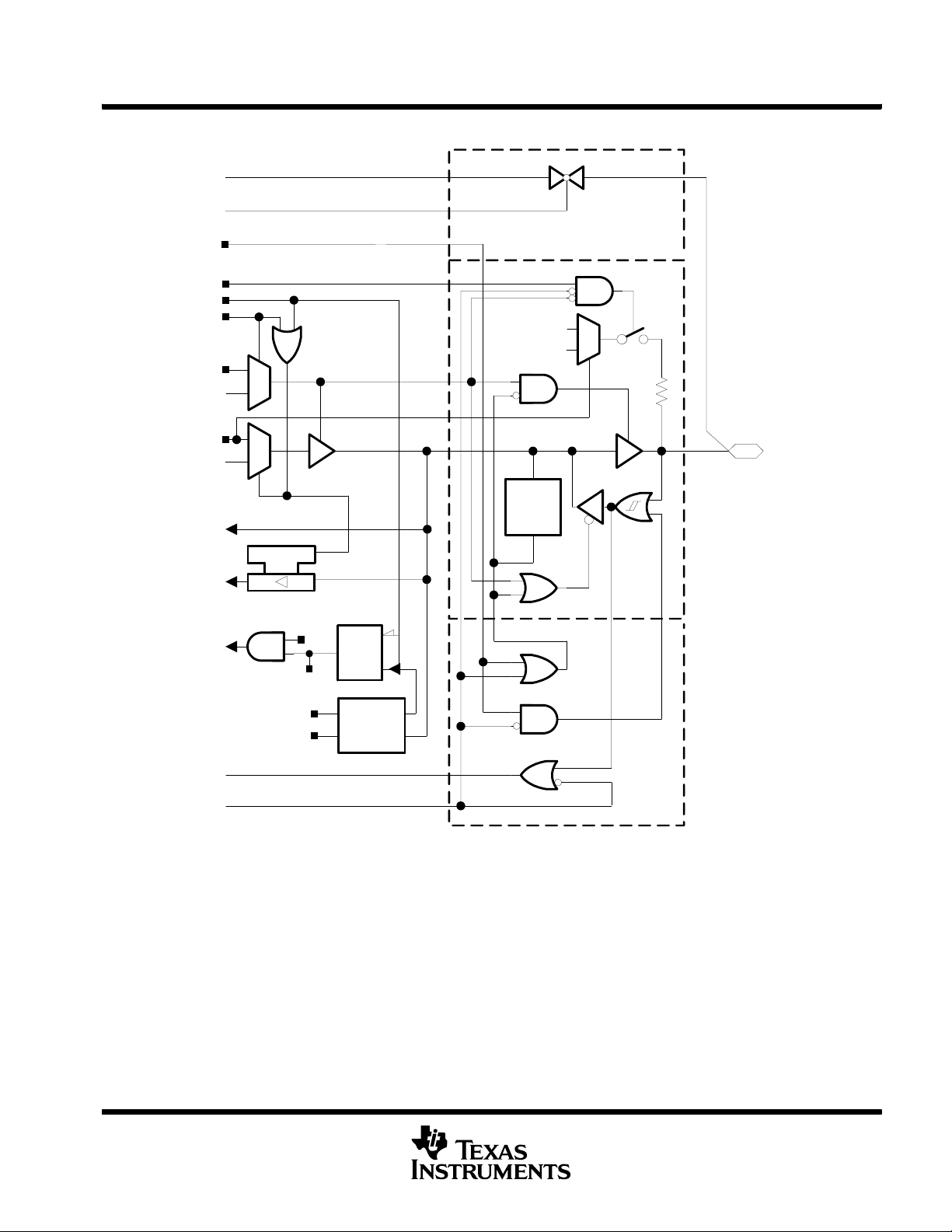
Port P1 (P1.5) pin schematics, MSP430x20x2
A5
INCHx = 5
ADC10AE.5
P1REN.5
P1SEL.5
USIPE5
P1DIR.5
USI Module Direction
0
1
Direction
0: Input
1: Output
MSP430x20x1, MSP430x20x2, MSP430x20x3
MIXED SIGNAL MICROCONTROLLER
SLAS491D -- AUGUST 2005 -- REVISED SEPTEMBER 2007
Pad Logic
DVSS
DVCC
0
1
1
P1OUT.5
Module X OUT
P1IN.5
Module X IN
P1IRQ.5
To JTA G
From JTAG
0
1
P1IE.5
P1IFG.5
P1SEL.5
P1IES.5
P1.5/TA0/SCLK/A5/TMS
Bus
Keeper
EN
EN
D
EN
Q
Set
Interrupt
Edge
Select
POST OFFICE BOX 655303 • DALLAS, TEXAS 75265
63
Page 64

MSP430x20x1, MSP430x20x2, MSP430x20x3
MIXED SIGNAL MICROCONTROLLER
SLAS491D -- AUGUST 2005 -- REVISED SEPTEMBER 2007
Port P1 (P1.6) pin schematics, MSP430x20x2
A6
INCHx = 6
ADC10AE.6
P1REN.6
P1SEL.6
USIPE6
P1DIR.6
USI Module Direction
0
1
Direction
0: Input
1: Output
DVSS
DVCC
0
1
Pad Logic
1
P1OUT.6
Module X OUT
USI Module Output
(I2C Mode)
P1IN.6
Module X IN
P1IRQ.6
To JTA G
From JTAG
0
1
P1IE.6
P1IFG.6
P1SEL.6
P1IES.6
P1.6/TA1/SDO/SCL/A6/TDI
Bus
Keeper
EN
EN
D
EN
Q
Set
Interrupt
Edge
Select
64
POST OFFICE BOX 655303 • DALLAS, TEXAS 75265
Page 65

Port P1 (P1.7) pin schematics, MSP430x20x2
A7
INCHx = 7
ADC10AE.7
P1REN.7
P1SEL.7
USIPE7
P1DIR.7
USI Module Direction
0
1
Direction
0: Input
1: Output
MSP430x20x1, MSP430x20x2, MSP430x20x3
MIXED SIGNAL MICROCONTROLLER
SLAS491D -- AUGUST 2005 -- REVISED SEPTEMBER 2007
Pad Logic
DVSS
DVCC
0
1
1
P1OUT.7
Module X OUT
USI Module Output
(I2C Mode)
P1IN.7
Module X IN
P1IRQ.7
To JTA G
From JTAG
From JTAG
0
1
P1IE.7
P1IFG.7
P1SEL.7
P1IES.7
P1.7/SDI/SDA/A7/TDO/TDI
Bus
Keeper
EN
EN
D
EN
Q
Set
Interrupt
Edge
Select
From JTAG (TDO)
POST OFFICE BOX 655303 • DALLAS, TEXAS 75265
65
Page 66

MSP430x20x1, MSP430x20x2, MSP430x20x3
X
/
/
MIXED SIGNAL MICROCONTROLLER
SLAS491D -- AUGUST 2005 -- REVISED SEPTEMBER 2007
Port P2 (P2.6) pin schematics, MSP430x20x2
LFXT1 off
LFXT1CLK
P2SEL.7
P2REN.6
P2DIR.6
P2OUT.6
Module X OUT
P2SEL.6
P2IN.6
BCSCTL3.LFXT1Sx = 11
0
1
0
1
0
1
EN
Direction
0: Input
1: Output
LFXT1 Oscillator
DVSS
DVCC
Bus
Keeper
EN
0
1
P2.7/XOUT
Pad Logic
1
P2.6/XIN/TA1
Module X IN
P2IRQ.6
P2IE.6
P2IFG.6
P2SEL.6
P2IES.6
D
EN
Q
Set
Interrupt
Edge
Select
Port P2 (P2.6) pin functions, MSP430x20x2
PIN NAME (P2.X)
P2.6/XIN/TA1 6
†
Default after reset (PUC/POR)
NOTES: 1. N/A: Not available or not applicable.
2. X: Don’t care.
3. XIN is used as digital clock input if the bits LFXT1Sx in register BCSCTL3 are set to 11.
P2.6 Input/Output 0/1 0
XIN† (see Note 3) 0 1
Timer_A2.TA1 1 1
FUNCTION
CONTROL BITS / SIGNALS
P2DIR.x P2SEL.x
66
POST OFFICE BOX 655303 • DALLAS, TEXAS 75265
Page 67

Port P2 (P2.7) pin schematics, MSP430x20x2
X
/
MSP430x20x1, MSP430x20x2, MSP430x20x3
MIXED SIGNAL MICROCONTROLLER
SLAS491D -- AUGUST 2005 -- REVISED SEPTEMBER 2007
LFXT1 off
LFXT1CLK
P2SEL.6
P2REN.7
P2DIR.7
P2OUT.7
Module X OUT
P2SEL.7
P2IN.7
BCSCTL3.LFXT1Sx = 11
0
1
0
1
0
1
EN
From P2.6/XIN
Direction
0: Input
1: Output
LFXT1 Oscillator
DVSS
DVCC
Bus
Keeper
EN
0
1
P2.6/XIN/TA1
Pad Logic
1
P2.7/XOUT
Module X IN
P2IRQ.7
P2IE.7
P2IFG.7
P2SEL.7
P2IES.7
D
EN
Q
Set
Interrupt
Edge
Select
Port P2 (P2.7) pin functions, MSP430x20x2
PIN NAME (P2.X)
P2.7/XOUT 7
†
Default after reset (PUC/POR)
NOTES: 1. N/A: Not available or not applicable.
2. X: Don’t care.
3. If the pin P2.7/XOUT is used as an input a current can flow until P2SEL.7 is cleared due to the oscillator output driver connection
to this pin after reset.
P2.7 Input/Output 0/1 0
DVSS 0 1
XOUT†(seeNote3) 1 1
FUNCTION
CONTROL BITS / SIGNALS
P2DIR.x P2SEL.x
POST OFFICE BOX 655303 • DALLAS, TEXAS 75265
67
Page 68

MSP430x20x1, MSP430x20x2, MSP430x20x3
X
///
///
///
/
/
MIXED SIGNAL MICROCONTROLLER
SLAS491D -- AUGUST 2005 -- REVISED SEPTEMBER 2007
APPLICATION INFORMATION, MSP430x20x3
Port P1 (P1.0 to P1.3) pin functions, MSP430x20x3
PIN NAME (P1.X)
P1.0/TACLK/ACLK/A0+ 0
P1.1/TA0/A0--/A4+ 1
P1.2/TA1/A1+/A4-- 2
P1.3/VREF/A1-- 3
†
Default after reset (PUC/POR)
NOTES: 1. N/A: Not available or not applicable.
2. X: Don’t care.
3. Setting the SD16AE.x bit disables the output driver as well as the input schmitt trigger to prevent parasitic cross currents when
applying analog signals.
4. With SD16AE.x = 0 the negative inputs are connected to VSS if the corresponding input is selected.
P1.0† Input/Output 0/1 0 0 N/A
Timer_A2.TACLK/INCLK 0 1 0 N/A
ACLK 1 1 0 N/A
A0+(seeNote3) X X 1 0
P1.1† Input/Output 0/1 0 0 N/A
Timer_A2.CCI0A 0 1 0 N/A
Timer_A2.TA0 1 1 0 N/A
A0-- (see Notes 3, 4) X X 1 0
A4+(seeNote3) X X 1 4
P1.2† Input/Output 0/1 0 0 N/A
Timer_A2.CCI1A 0 1 0 N/A
Timer_A2.TA1 1 1 0 N/A
A1+(seeNote3) X X 1 1
A4-- (see Notes 3, 4) X X 1 4
P1.3† Input/Output 0/1 0 0 N/A
VREF X 1 0 N/A
A1-- (see Notes 3, 4) X X 1 1
FUNCTION
CONTROL BITS / SIGNALS
P1DIR.x P1SEL.x SD16AE.x INCHx
68
POST OFFICE BOX 655303 • DALLAS, TEXAS 75265
Page 69

Port P1 (P1.0) pin schematics, MSP430x20x3
=0
INCH
A0+
.0
16AE
SD
P1
.0
REN
MSP430x20x1, MSP430x20x2, MSP430x20x3
MIXED SIGNAL MICROCONTROLLER
SLAS491D -- AUGUST 2005 -- REVISED SEPTEMBER 2007
Pad Logic
P1
DIR
P1OUT.0
Module X OUT
P1SEL.0
P1IN.0
Module X IN
P1
IRQ
DVSS
DVCC
.0
0
1
0
1
EN
D
P1IE.0
.0
P1
IFG
P1SEL.0
P1
.0
IES
.0
Direction
0: Input
1: Output
Bus
Keeper
EN
EN
Q
Set
Interrupt
Edge
Select
0
1
1
P1.0/
TAC L K/ACLK
/A0+
POST OFFICE BOX 655303 • DALLAS, TEXAS 75265
69
Page 70

MSP430x20x1, MSP430x20x2, MSP430x20x3
MIXED SIGNAL MICROCONTROLLER
SLAS491D -- AUGUST 2005 -- REVISED SEPTEMBER 2007
Port P1 (P1.1) pin schematics, MSP430x20x3
=4
INCH
A4+
=0
INCH
0
AV
SS
SD
P1
16
REN
AE
A0--
1
.1
.1
Pad Logic
P1
DIR
P1OUT.1
Module X OUT
P1SEL.1
P1IN.1
Module X IN
P1
IRQ
DVSS
DVCC
.1
0
1
0
1
EN
D
P1IE.1
.1
P1
IFG
P1SEL.1
P1
.1
IES
.1
Direction
0: Input
1: Output
Bus
Keeper
EN
EN
Q
Set
Interrupt
Edge
Select
0
1
1
P1.1/TA0/A0--/A4+
70
POST OFFICE BOX 655303 • DALLAS, TEXAS 75265
Page 71

Port P1 (P1.2) pin schematics, MSP430x20x3
=1
INCH
A1+
=4
INCH
0
AV
SS
SD
P1
16
REN
AE
A4--
.2
.2
1
MSP430x20x1, MSP430x20x2, MSP430x20x3
MIXED SIGNAL MICROCONTROLLER
SLAS491D -- AUGUST 2005 -- REVISED SEPTEMBER 2007
Pad Logic
P1
DIR
P1OUT.2
Module X OUT
P1SEL.2
P1IN.2
Module X IN
P1
IRQ
DVSS
DVCC
.2
0
1
0
1
EN
D
P1IE.2
.2
P1
IFG
P1SEL.2
P1
.2
IES
.2
Direction
0: Input
1: Output
Bus
Keeper
EN
EN
Q
Set
Interrupt
Edge
Select
0
1
1
P1.2/TA1/A1+/A4--
POST OFFICE BOX 655303 • DALLAS, TEXAS 75265
71
Page 72

MSP430x20x1, MSP430x20x2, MSP430x20x3
MIXED SIGNAL MICROCONTROLLER
SLAS491D -- AUGUST 2005 -- REVISED SEPTEMBER 2007
Port P1 (P1.3) pin schematics, MSP430x20x3
V
REF
=1
INCH
0
AV
SS
SD
P1
16
REN
AE
A1--
1
.3
.3
Pad Logic
P1
DIR
P1OUT.3
P1SEL.3
P1IN.3
P1
IRQ
DVSS
DVCC
.3
0
1
0
1
P1IE.3
.3
P1
P1SEL.3
P1
IES
.3
IFG
Direction
0: Input
1: Output
.3
Bus
Keeper
EN
EN
Q
Set
Interrupt
Edge
Select
0
1
1
P1.3/VREF/A1--
72
POST OFFICE BOX 655303 • DALLAS, TEXAS 75265
Page 73

Port P1 (P1.4 to P1.7) pin functions, MSP430x20x3
///
///
/
/////
///
/
PIN NAME (P1.X)
P1.4/SMCLK/A2+/ 4
TCK
P1.5/TA0/SCLK/A2--/ 5
TMS
P1.6/TA1/SDO/SCL/A3+/ 6
TDI
P1.7/SDI/SDA/A3--/ 7
TDO/TDI
†
Default after reset (PUC/POR)
NOTES: 1. N/A: Not available or not applicable.
2. X: Don’t care.
3. Setting the SD16AE.x bit disables the output driver as well as the input schmitt trigger to prevent parasitic cross currents when
applying analog signals.
4. With SD16AE.x = 0 the negative inputs are connected to VSS if the corresponding input is selected.
5. In JTAG mode the internal pull-up/down resistors are disabled.
6. Function controlled by JTAG
X FUNCTION
P1.4† Input/Output 0/1 0 N/A 0 N/A 0
N/A 0 1 N/A 0 N/A 0
SMCLK 1 1 N/A 0 N/A 0
A2+(seeNote3) X X N/A 1 2 0
TCK(seeNote5) X X N/A X X 1
P1.5† Input/Output 0/1 0 X 0 N/A 0
N/A 0 1 X 0 N/A 0
Timer_A2.TA0 1 1 X 0 N/A 0
SCLK X X 1 0 N/A 0
A2-- (see Notes 3, 4) X X X 1 2 0
TMS(seeNote5) X X X X X 1
P1.6† Input/Output 0/1 0 X 0 N/A 0
Timer_A2.CCI1B 0 1 X 0 N/A 0
Timer_A2.TA1 1 1 X 0 N/A 0
SDO (SPI) / SCL (I2C) X X 1 0 N/A 0
A3+(seeNote3) X X X 1 3 0
TDI(seeNote5) X X X X X 1
P1.7† Input/Output 0/1 0 X 0 N/A 0
N/A 0 1 X 0 N/A 0
DVSS 1 1 X 0 N/A 0
SDI (SPI) / SDA (I2C) X X 1 0 N/A 0
A3-- (see Notes 3, 4) X X X 1 3 0
TDO/TDI (see Notes 5, 6) X X X X X 1
P1DIR.x P1SEL.x USIP.x SD16AE.x INCHx
MSP430x20x1, MSP430x20x2, MSP430x20x3
MIXED SIGNAL MICROCONTROLLER
SLAS491D -- AUGUST 2005 -- REVISED SEPTEMBER 2007
CONTROL BITS / SIGNALS
JTAG
Mode
POST OFFICE BOX 655303 • DALLAS, TEXAS 75265
73
Page 74

MSP430x20x1, MSP430x20x2, MSP430x20x3
MIXED SIGNAL MICROCONTROLLER
SLAS491D -- AUGUST 2005 -- REVISED SEPTEMBER 2007
Port P1 (P1.4) pin schematics, MSP430x20x3
=2
INCH
A2+
.4
AE
16
SD
P1
.4
REN
Pad Logic
P1
DIR
P1OUT.4
Module X OUT
P1SEL.4
P1IN.4
Module X IN
P1
IRQ
To JTA G
DVSS
DVCC
.4
0
1
0
1
EN
D
P1IE.4
.4
P1
IFG
P1SEL.4
P1
.4
IES
.4
Direction
0: Input
1: Output
Bus
Keeper
EN
EN
Q
Set
Interrupt
Edge
Select
0
1
1
P1.4/
SMCLK
/A2+/
TCK
From JTAG
74
POST OFFICE BOX 655303 • DALLAS, TEXAS 75265
Page 75

Port P1 (P1.5) pin schematics, MSP430x20x3
MSP430x20x1, MSP430x20x2, MSP430x20x3
MIXED SIGNAL MICROCONTROLLER
SLAS491D -- AUGUST 2005 -- REVISED SEPTEMBER 2007
=2
INCH
A2--
16AE
SD
P1
REN
P1SEL.5
USIPE
P1
DIR
USI Module Direction
P1OUT.5
Module X OUT
P1IN.5
Module X IN
Pad Logic
0
AV
SS
1
.5
.5
5
.5
0
1
0
1
EN
Direction
0: Input
1: Output
D
DVSS
DVCC
Bus
Keeper
EN
0
1
1
P1.5/TA0/
SCLK
/A2--/
TMS
P1
IRQ
To JTA G
From JTAG
P1IE.5
.5
P1
IFG
P1SEL.5
P1
.5
IES
.5
EN
Q
Set
Interrupt
Edge
Select
POST OFFICE BOX 655303 • DALLAS, TEXAS 75265
75
Page 76

MSP430x20x1, MSP430x20x2, MSP430x20x3
MIXED SIGNAL MICROCONTROLLER
SLAS491D -- AUGUST 2005 -- REVISED SEPTEMBER 2007
Port P1 (P1.6) pin schematics, MSP430x20x3
=3
INCH
A3+
AE
16
SD
P1
REN
P1SEL.6
USIPE
P1
DIR
USI Module Direction
P1OUT.6
Module X OUT
USI Module Output
2
(I
C Mode
P1IN.6
Pad Logic
.6
.6
6
.6
0
1
0
1
)
EN
Direction
0: Input
1: Output
DVSS
DVCC
Bus
Keeper
EN
0
1
1
P1.6/TA1/
/SCL/A3+/TDI
SDO
Module X IN
P1
IRQ
To JTA G
From JTAG
D
P1IE.6
.6
P1
IFG
P1SEL.6
P1
.6
IES
.6
EN
Q
Set
Interrupt
Edge
Select
76
POST OFFICE BOX 655303 • DALLAS, TEXAS 75265
Page 77

Port P1 (P1.7) pin schematics, MSP430x20x3
MSP430x20x1, MSP430x20x2, MSP430x20x3
MIXED SIGNAL MICROCONTROLLER
SLAS491D -- AUGUST 2005 -- REVISED SEPTEMBER 2007
=3
INCH
A3--
16AE
SD
P1
REN
P1SEL.x
USIPE
P1
DIR
USI Module Direction
P1OUT.x
Module X OUT
USI Module Output
2
(I
C Mode
P1IN.x
Pad Logic
0
AV
SS
1
.x
.x
7
.x
0
1
0
1
)
EN
Direction
0: Input
1: Output
DVSS
DVCC
Bus
Keeper
EN
0
1
1
P1.7/SDI/
SDA
/A3--/
TDO
/TDI
Module X IN
P1
To JTA G
From JTAG
From JTAG
From JTAG (
IRQ
TDO
D
P1IE.x
.x
P1
IFG
P1SEL.x
P1
.x
IES
)
.x
EN
Q
Set
Interrupt
Edge
Select
POST OFFICE BOX 655303 • DALLAS, TEXAS 75265
77
Page 78

MSP430x20x1, MSP430x20x2, MSP430x20x3
X
/
/
MIXED SIGNAL MICROCONTROLLER
SLAS491D -- AUGUST 2005 -- REVISED SEPTEMBER 2007
Port P2 (P2.6) pin schematics, MSP430x20x3
LFXT1 off
LFXT1CLK
P2SEL.7
P2REN.6
P2DIR.6
P2OUT.6
Module X OUT
P2SEL.6
P2IN.6
BCSCTL3.LFXT1Sx = 11
0
1
0
1
0
1
EN
Direction
0: Input
1: Output
LFXT1 Oscillator
DVSS
DVCC
Bus
Keeper
EN
0
1
P2.7/XOUT
Pad Logic
1
P2.6/XIN/TA1
Module X IN
P2IRQ.6
P2IE.6
P2IFG.6
P2SEL.6
P2IES.6
D
EN
Q
Set
Interrupt
Edge
Select
Port P2 (P2.6) pin functions, MSP430x20x3
PIN NAME (P2.X)
P2.6/XIN/TA1 6
†
Default after reset (PUC/POR)
NOTES: 1. N/A: Not available or not applicable.
2. X: Don’t care.
3. XIN is used as digital clock input if the bits LFXT1Sx in register BCSCTL3 are set to 11.
P2.6 Input/Output 0/1 0
XIN† (see Note 3) 0 1
Timer_A2.TA1 1 1
FUNCTION
CONTROL BITS / SIGNALS
P2DIR.x P2SEL.x
78
POST OFFICE BOX 655303 • DALLAS, TEXAS 75265
Page 79

Port P2 (P2.7) pin schematics, MSP430x20x3
X
/
MSP430x20x1, MSP430x20x2, MSP430x20x3
MIXED SIGNAL MICROCONTROLLER
SLAS491D -- AUGUST 2005 -- REVISED SEPTEMBER 2007
LFXT1 off
LFXT1CLK
P2SEL.6
P2REN.7
P2DIR.7
P2OUT.7
Module X OUT
P2SEL.7
P2IN.7
BCSCTL3.LFXT1Sx = 11
0
1
0
1
0
1
EN
From P2.6/XIN
Direction
0: Input
1: Output
LFXT1 Oscillator
DVSS
DVCC
Bus
Keeper
EN
0
1
P2.6/XIN/TA1
Pad Logic
1
P2.7/XOUT
Module X IN
P2IRQ.7
P2IE.7
P2IFG.7
P2SEL.7
P2IES.7
D
EN
Q
Set
Interrupt
Edge
Select
Port P2 (P2.7) pin functions, MSP430x20x3
PIN NAME (P2.X)
P2.7/XOUT 7
†
Default after reset (PUC/POR)
NOTES: 1. N/A: Not available or not applicable.
2. X: Don’t care.
3. If the pin P2.7/XOUT is used as an input a current can flow until P2SEL.7 is cleared due to the oscillator output driver connection
to this pin after reset.
P2.7 Input/Output 0/1 0
DVSS 0 1
XOUT†(seeNote3) 1 1
FUNCTION
CONTROL BITS / SIGNALS
P2DIR.x P2SEL.x
POST OFFICE BOX 655303 • DALLAS, TEXAS 75265
79
Page 80

MSP430x20x1, MSP430x20x2, MSP430x20x3
MIXED SIGNAL MICROCONTROLLER
SLAS491D -- AUGUST 2005 -- REVISED SEPTEMBER 2007
Data Sheet Revision History
Literature
Number
SLAS491 Preliminary PRODUCT PREVIEW data sheet release
SLAS491A Production data sheet release for MSP430x20x3I.
SLAS491B Production data sheet release for MSP430x20x3T, MSP430x20x1I and MSP430x20x1T.
SLAS491C Production data sheet release for MSP430x20x2I and MSP430x20x2T.
SLAS491D Changed f
Updated specification and added characterization graphs.
105°C characterization results added.
SD16_A SINAD characterization results for MSP430x20x3RSA package added.
Updated SD16_A Power Supply Rejection specification.
DCO Calibration Register names: lower case “z” changed to upper case “Z”.
V
hys(B_IT--)
MIN and MAX percentages for “calibrated DCO frequencies -- tolerance over supply voltage VCC” corrected from 2.5% to
3.0% to match the specified frequency ranges.
MAX specification increased from 180mV to 210mV.
ACLK
to0HzinI
test conditions on page 23.
LPM4
Summary
80
POST OFFICE BOX 655303 • DALLAS, TEXAS 75265
Page 81

PACKAGE OPTION ADDENDUM
www.ti.com
PACKAGING INFORMATION
Orderable Device Status
MSP430F2001IN ACTIVE PDIP N 14 25 Pb-Free
MSP430F2001IPW ACTIVE TSSOP PW 14 90 Green (RoHS &
MSP430F2001IPWR ACTIVE TSSOP PW 14 2000 Green (RoHS &
MSP430F2001IRSAR ACTIVE QFN RSA 16 3000 Green (RoHS &
MSP430F2001IRSAT ACTIVE QFN RSA 16 250 Green (RoHS &
MSP430F2001TN ACTIVE PDIP N 14 25 Pb-Free
MSP430F2001TPW ACTIVE TSSOP PW 14 90 Green (RoHS &
MSP430F2001TPWR ACTIVE TSSOP PW 14 2000 Green (RoHS &
MSP430F2001TRSAR ACTIVE QFN RSA 16 3000 Green (RoHS &
MSP430F2001TRSAT ACTIVE QFN RSA 16 250 Green (RoHS &
MSP430F2002IN ACTIVE PDIP N 14 25 Pb-Free
MSP430F2002IPW ACTIVE TSSOP PW 14 90 Green (RoHS &
MSP430F2002IPWR ACTIVE TSSOP PW 14 2000 Green (RoHS &
MSP430F2002IRSAR ACTIVE QFN RSA 16 3000 Green (RoHS &
MSP430F2002IRSAT ACTIVE QFN RSA 16 250 Green (RoHS &
MSP430F2002TN ACTIVE PDIP N 14 25 Pb-Free
MSP430F2002TPW ACTIVE TSSOP PW 14 90 Green (RoHS &
MSP430F2002TPWR ACTIVE TSSOP PW 14 2000 Green (RoHS &
MSP430F2002TRSAR ACTIVE QFN RSA 16 3000 Green (RoHS &
MSP430F2002TRSAT ACTIVE QFN RSA 16 250 Green (RoHS &
MSP430F2003IN ACTIVE PDIP N 14 25 Pb-Free
MSP430F2003IPW ACTIVE TSSOP PW 14 90 Green (RoHS &
MSP430F2003IPWR ACTIVE TSSOP PW 14 2000 Green (RoHS &
MSP430F2003IRSAR ACTIVE QFN RSA 16 3000 Green (RoHS &
MSP430F2003IRSAT ACTIVE QFN RSA 16 250 Green (RoHS &
(1)
Package
Type
Package
Drawing
Pins Package
Qty
Eco Plan
(RoHS)
no Sb/Br)
no Sb/Br)
no Sb/Br)
no Sb/Br)
(RoHS)
no Sb/Br)
no Sb/Br)
no Sb/Br)
no Sb/Br)
(RoHS)
no Sb/Br)
no Sb/Br)
no Sb/Br)
no Sb/Br)
(RoHS)
no Sb/Br)
no Sb/Br)
no Sb/Br)
no Sb/Br)
(RoHS)
no Sb/Br)
no Sb/Br)
no Sb/Br)
no Sb/Br)
(2)
Lead/Ball Finish MSL Peak Temp
CU NIPDAU Level-1-260C-UNLIM
CU NIPDAU Level-1-260C-UNLIM
CU NIPDAU Level-1-260C-UNLIM
CU NIPDAU Level-2-260C-1 YEAR
CU NIPDAU Level-2-260C-1 YEAR
CU NIPDAU Level-1-260C-UNLIM
CU NIPDAU Level-1-260C-UNLIM
CU NIPDAU Level-1-260C-UNLIM
CU NIPDAU Level-2-260C-1 YEAR
CU NIPDAU Level-2-260C-1 YEAR
CU NIPDAU Level-1-260C-UNLIM
CU NIPDAU Level-1-260C-UNLIM
CU NIPDAU Level-1-260C-UNLIM
CU NIPDAU Level-2-260C-1 YEAR
CU NIPDAU Level-2-260C-1 YEAR
CU NIPDAU Level-1-260C-UNLIM
CU NIPDAU Level-1-260C-UNLIM
CU NIPDAU Level-1-260C-UNLIM
CU NIPDAU Level-2-260C-1 YEAR
CU NIPDAU Level-2-260C-1 YEAR
CU NIPDAU Level-1-260C-UNLIM
CU NIPDAU Level-1-260C-UNLIM
CU NIPDAU Level-1-260C-UNLIM
CU NIPDAU Level-2-260C-1 YEAR
CU NIPDAU Level-2-260C-1 YEAR
11-Jun-2007
(3)
Addendum-Page 1
Page 82

PACKAGE OPTION ADDENDUM
www.ti.com
Orderable Device Status
(1)
Package
Type
Package
Drawing
Pins Package
Qty
Eco Plan
(2)
MSP430F2003TN ACTIVE PDIP N 14 25 Pb-Free
(RoHS)
MSP430F2003TPW ACTIVE TSSOP PW 14 90 Green (RoHS &
no Sb/Br)
MSP430F2003TPWR ACTIVE TSSOP PW 14 2000 Green (RoHS &
no Sb/Br)
MSP430F2003TRSAR ACTIVE QFN RSA 16 3000 Green (RoHS &
no Sb/Br)
MSP430F2003TRSAT ACTIVE QFN RSA 16 250 Green (RoHS &
no Sb/Br)
MSP430F2011IN ACTIVE PDIP N 14 25 Pb-Free
(RoHS)
MSP430F2011IPW ACTIVE TSSOP PW 14 90 Green (RoHS &
no Sb/Br)
MSP430F2011IPWR ACTIVE TSSOP PW 14 2000 Green (RoHS &
no Sb/Br)
MSP430F2011IRSAR ACTIVE QFN RSA 16 3000 Green (RoHS &
no Sb/Br)
MSP430F2011IRSAT ACTIVE QFN RSA 16 250 Green (RoHS &
no Sb/Br)
MSP430F2011TN ACTIVE PDIP N 14 25 Pb-Free
(RoHS)
MSP430F2011TPW ACTIVE TSSOP PW 14 90 Green (RoHS &
no Sb/Br)
MSP430F2011TPWR ACTIVE TSSOP PW 14 2000 Green (RoHS &
no Sb/Br)
MSP430F2011TRSAR ACTIVE QFN RSA 16 3000 Green (RoHS &
no Sb/Br)
MSP430F2011TRSAT ACTIVE QFN RSA 16 250 Green (RoHS &
no Sb/Br)
MSP430F2012IN ACTIVE PDIP N 14 25 Pb-Free
(RoHS)
MSP430F2012IPW ACTIVE TSSOP PW 14 90 Green (RoHS &
no Sb/Br)
MSP430F2012IPWR ACTIVE TSSOP PW 14 2000 Green (RoHS &
no Sb/Br)
MSP430F2012IRSAR ACTIVE QFN RSA 16 3000 Green (RoHS &
no Sb/Br)
MSP430F2012IRSAT ACTIVE QFN RSA 16 250 Green (RoHS &
no Sb/Br)
MSP430F2012TN ACTIVE PDIP N 14 25 Pb-Free
(RoHS)
MSP430F2012TPW ACTIVE TSSOP PW 14 90 Green (RoHS &
no Sb/Br)
MSP430F2012TPWR ACTIVE TSSOP PW 14 2000 Green (RoHS &
no Sb/Br)
MSP430F2012TRSAR ACTIVE QFN RSA 16 3000 Green (RoHS &
no Sb/Br)
MSP430F2012TRSAT ACTIVE QFN RSA 16 250 Green (RoHS &
no Sb/Br)
MSP430F2013IN ACTIVE PDIP N 14 25 Pb-Free
(RoHS)
11-Jun-2007
Lead/Ball Finish MSL Peak Temp
CU NIPDAU Level-1-260C-UNLIM
CU NIPDAU Level-1-260C-UNLIM
CU NIPDAU Level-1-260C-UNLIM
CU NIPDAU Level-2-260C-1 YEAR
CU NIPDAU Level-2-260C-1 YEAR
CU NIPDAU Level-1-260C-UNLIM
CU NIPDAU Level-1-260C-UNLIM
CU NIPDAU Level-1-260C-UNLIM
CU NIPDAU Level-2-260C-1 YEAR
CU NIPDAU Level-2-260C-1 YEAR
CU NIPDAU Level-1-260C-UNLIM
CU NIPDAU Level-1-260C-UNLIM
CU NIPDAU Level-1-260C-UNLIM
CU NIPDAU Level-2-260C-1 YEAR
CU NIPDAU Level-2-260C-1 YEAR
CU NIPDAU Level-1-260C-UNLIM
CU NIPDAU Level-1-260C-UNLIM
CU NIPDAU Level-1-260C-UNLIM
CU NIPDAU Level-2-260C-1 YEAR
CU NIPDAU Level-2-260C-1 YEAR
CU NIPDAU Level-1-260C-UNLIM
CU NIPDAU Level-1-260C-UNLIM
CU NIPDAU Level-1-260C-UNLIM
CU NIPDAU Level-2-260C-1 YEAR
CU NIPDAU Level-2-260C-1 YEAR
CU NIPDAU Level-1-260C-UNLIM
(3)
Addendum-Page 2
Page 83

PACKAGE OPTION ADDENDUM
www.ti.com
Orderable Device Status
(1)
Package
Type
Package
Drawing
Pins Package
Qty
Eco Plan
(2)
MSP430F2013IPW ACTIVE TSSOP PW 14 90 Green (RoHS &
Lead/Ball Finish MSL Peak Temp
CU NIPDAU Level-1-260C-UNLIM
11-Jun-2007
(3)
no Sb/Br)
MSP430F2013IPWR ACTIVE TSSOP PW 14 2000 Green (RoHS &
CU NIPDAU Level-1-260C-UNLIM
no Sb/Br)
MSP430F2013IRSAR ACTIVE QFN RSA 16 3000 Green (RoHS &
CU NIPDAU Level-2-260C-1 YEAR
no Sb/Br)
MSP430F2013IRSAT ACTIVE QFN RSA 16 250 Green (RoHS &
CU NIPDAU Level-2-260C-1 YEAR
no Sb/Br)
MSP430F2013TN ACTIVE PDIP N 14 25 Pb-Free
CU NIPDAU Level-1-260C-UNLIM
(RoHS)
MSP430F2013TPW ACTIVE TSSOP PW 14 90 Green (RoHS &
CU NIPDAU Level-1-260C-UNLIM
no Sb/Br)
MSP430F2013TPWR ACTIVE TSSOP PW 14 2000 Green (RoHS &
CU NIPDAU Level-1-260C-UNLIM
no Sb/Br)
MSP430F2013TRSAR ACTIVE QFN RSA 16 3000 Green (RoHS &
CU NIPDAU Level-2-260C-1 YEAR
no Sb/Br)
MSP430F2013TRSAT ACTIVE QFN RSA 16 250 Green (RoHS &
CU NIPDAU Level-2-260C-1 YEAR
no Sb/Br)
(1)
The marketing status values are defined as follows:
ACTIVE: Product device recommended for new designs.
LIFEBUY: TI has announced that the device will be discontinued, and a lifetime-buy period is in effect.
NRND: Not recommended for new designs. Device is in production to support existing customers, but TI does not recommend using this part in
a new design.
PREVIEW: Device has been announced but is not in production. Samples may or may not be available.
OBSOLETE: TI has discontinued the production of the device.
(2)
Eco Plan - The planned eco-friendly classification: Pb-Free (RoHS), Pb-Free (RoHS Exempt), or Green (RoHS & no Sb/Br) - please check
http://www.ti.com/productcontent for the latest availability information and additional product content details.
TBD: The Pb-Free/Green conversion plan has not been defined.
Pb-Free (RoHS): TI's terms "Lead-Free" or "Pb-Free" mean semiconductor products that are compatible with the current RoHS requirements
for all 6 substances, including the requirement that lead not exceed 0.1% by weight in homogeneous materials. Where designed to be soldered
at high temperatures, TI Pb-Free products are suitable for use in specified lead-free processes.
Pb-Free (RoHS Exempt): This component has a RoHS exemption for either 1) lead-based flip-chip solder bumps used between the die and
package, or 2) lead-based die adhesive used between the die and leadframe. The component is otherwise considered Pb-Free (RoHS
compatible) as defined above.
Green (RoHS & no Sb/Br): TI defines "Green" to mean Pb-Free (RoHS compatible), and free of Bromine (Br) and Antimony (Sb) based flame
retardants (Br or Sb do not exceed 0.1% by weight in homogeneous material)
(3)
MSL, Peak Temp. -- The Moisture Sensitivity Level rating according to the JEDEC industry standard classifications, and peak solder
temperature.
Important Information and Disclaimer:The information provided on this page represents TI's knowledge and belief as of the date that it is
provided. TI bases its knowledge and belief on information provided by third parties, and makes no representation or warranty as to the
accuracy of such information. Efforts are underway to better integrate information from third parties. TI has taken and continues to take
reasonable steps to provide representative and accurate information but may not have conducted destructive testing or chemical analysis on
incoming materials and chemicals. TI and TI suppliers consider certain information to be proprietary, and thus CAS numbers and other limited
information may not be available for release.
In no event shall TI's liability arising out of such information exceed the total purchase price of the TI part(s) at issue in this document sold by TI
to Customer on an annual basis.
Addendum-Page 3
Page 84

Page 85

Page 86

Page 87

Page 88

MECHANICAL DATA
MTSS001C – JANUARY 1995 – REVISED FEBRUARY 1999
PW (R-PDSO-G**) PLASTIC SMALL-OUTLINE PACKAGE
14 PINS SHOWN
0,65
1,20 MAX
14
0,30
0,19
8
4,50
4,30
PINS **
7
Seating Plane
0,15
0,05
8
1
A
DIM
6,60
6,20
14
0,10
M
0,10
0,15 NOM
0°–8°
2016
Gage Plane
24
0,25
0,75
0,50
28
A MAX
A MIN
NOTES: A. All linear dimensions are in millimeters.
B. This drawing is subject to change without notice.
C. Body dimensions do not include mold flash or protrusion not to exceed 0,15.
D. Falls within JEDEC MO-153
3,10
2,90
5,10
4,90
5,10
4,90
6,60
6,40
7,90
7,70
9,80
9,60
4040064/F 01/97
POST OFFICE BOX 655303 • DALLAS, TEXAS 75265
Page 89

IMPORTANT NOTICE
Texas Instruments Incorporated and its subsidiaries (TI) reserve the right to make corrections, modifications, enhancements,
improvements, and other changes to its products and services at any time and to discontinue any product or service without notice.
Customers should obtain the latest relevant information before placing orders and should verify that such information is current and
complete. All products are sold subject to TI’s terms and conditions of sale supplied at the time of order acknowledgment.
TI warrants performance of its hardware products to the specifications applicable at the time of sale in accordance with TI’s
standard warranty. Testing and other quality control techniques are used to the extent TI deems necessary to support this
warranty. Except where mandated by government requirements, testing of all parameters of each product is not necessarily
performed.
TI assumes no liability for applications assistance or customer product design. Customers are responsible for their products and
applications using TI components. To minimize the risks associated with customer products and applications, customers should
provide adequate design and operating safeguards.
TI does not warrant or represent that any license, either express or implied, is granted under any TI patent right, copyright, mask
work right, or other TI intellectual property right relating to any combination, machine, or process in which TI products or services
are used. Information published by TI regarding third-party products or services does not constitute a license from TI to use such
products or services or a warranty or endorsement thereof. Use of such information may require a license from a third party under
the patents or other intellectual property of the third party, or a license from TI under the patents or other intellectual property of TI.
Reproduction of TI information in TI data books or data sheets is permissible only if reproduction is without alteration and is
accompanied by all associated warranties, conditions, limitations, and notices. Reproduction of this information with alteration is an
unfair and deceptive business practice. TI is not responsible or liable for such altered documentation. Information of third parties
may be subject to additional restrictions.
Resale of TI products or services with statements different from or beyond the parameters stated by TI for that product or service
voids all express and any implied warranties for the associated TI product or service and is an unfair and deceptive business
practice. TI is not responsible or liable for any such statements.
TI products are not authorized for use in safety-critical applications (such as life support) where a failure of the TI product would
reasonably be expected to cause severe personal injury or death, unless officers of the parties have executed an agreement
specifically governing such use. Buyers represent that they have all necessary expertise in the safety and regulatory ramifications
of their applications, and acknowledge and agree that they are solely responsible for all legal, regulatory and safety-related
requirements concerning their products and any use of TI products in such safety-critical applications, notwithstanding any
applications-related information or support that may be provided by TI. Further, Buyers must fully indemnify TI and its
representatives against any damages arising out of the use of TI products in such safety-critical applications.
TI products are neither designed nor intended for use in military/aerospace applications or environments unless the TI products are
specifically designated by TI as military-grade or "enhanced plastic." Only products designated by TI as military-grade meet military
specifications. Buyers acknowledge and agree that any such use of TI products which TI has not designated as military-grade is
solely at the Buyer's risk, and that they are solely responsible for compliance with all legal and regulatory requirements in
connection with such use.
TI products are neither designed nor intended for use in automotive applications or environments unless the specific TI products
are designated by TI as compliant with ISO/TS 16949 requirements. Buyers acknowledge and agree that, if they use any
non-designated products in automotive applications, TI will not be responsible for any failure to meet such requirements.
Following are URLs where you can obtain information on other Texas Instruments products and application solutions:
Products Applications
Amplifiers amplifier.ti.com Audio www.ti.com/audio
Data Converters dataconverter.ti.com Automotive www.ti.com/automotive
DSP dsp.ti.com Broadband www.ti.com/broadband
Interface interface.ti.com Digital Control www.ti.com/digitalcontrol
Logic logic.ti.com Military www.ti.com/military
Power Mgmt power.ti.com Optical Networking www.ti.com/opticalnetwork
Microcontrollers microcontroller.ti.com Security www.ti.com/security
RFID www.ti-rfid.com Telephony www.ti.com/telephony
Low Power www.ti.com/lpw Video & Imaging www.ti.com/video
Wireless
Wireless www.ti.com/wireless
Mailing Address: Texas Instruments, Post Office Box 655303, Dallas, Texas 75265
Copyright © 2007, Texas Instruments Incorporated
 Loading...