

MSP430x33x
MIXED SIGNAL MICROCONTROLLERS
SLAS163 – FEBRUARY 1998
1
POST OFFICE BOX 655303 • DALLAS, TEXAS 75265
D
Low Supply Voltage Range 2.5 V – 5.5 V
D
Low Operation Current, 400 mA at 1 MHz,
3 V
D
Ultra-Low Power Consumption (Standby
Mode Down to 0.1 µA)
D
Five Power-Saving Modes
D
Wake Up from Standby Mode in 6 µS
D
16-Bit RISC Architecture, 300 ns Instruction
Cycle Time
D
Single Common 32 kHz Crystal, Internal
System Clock up to 3.8 MHz
D
Integrated LCD Driver for up to 120
Segments
D
Integrated Hardware Multiplier Performs
Signed, Unsigned, and MAC Operations for
Operands Up to 16 X 16 Bits
D
Serial Communication Interface (USART),
Select Asynchronous UART or
Synchronous SPI by Software
D
Slope A/D Converter Using External
Components
D
16-Bit Timer With Five Capture/Compare
Registers
D
Programmable Code Protection by Security
Fuse
D
Family Members Include:
MSP430C336 – 24 KB ROM, 1 KB RAM
MSP430C337 – 32 KB ROM, 1 KB RAM
MSP430P337 – 32 KB OTP, 1 KB RAM
D
EPROM Version Available for Prototyping:
PMS430E337
D
Serial On-Board Programming
D
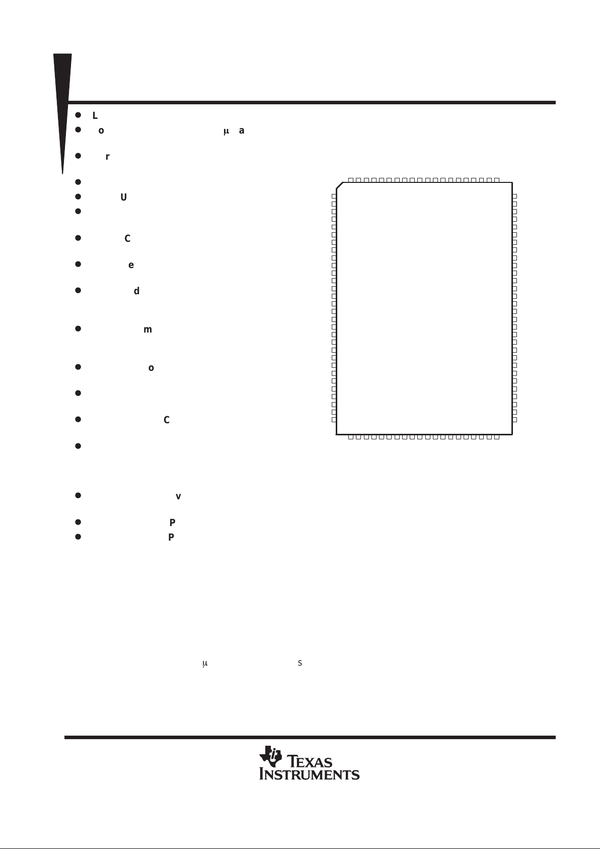
Available in 100 Pin Quad Flat-Pack (QFP)
Package, 100 Pin Ceramic Quad Flat-Pack
(CFP) package (EPROM Version)
description
The T exas Instruments MSP430 series is a ultra low-power microcontroller family consisting of several devices
which features different sets of modules targeted to various applications. The controller is designed to be battery
operated for an extended application lifetime. With the 16-bit RISC architecture, 16 integrated registers on the
CPU, and the constant generator, the MSP430 achieves maximum code efficiency. The digital-controlled
oscillator, together with the frequency lock loop (FLL), provides a fast wake up from a low-power mode to an
active mode in less than 6 ms. The MSP430x33x series micro-controllers have built in hardware multiplication
and communication capability using asynchronous (UART) and synchronous protocols.
Typical applications of the MSP430 family include electronic gas, water, and electric meters and other sensor
systems that capture analog signals, converts them to digital values, processes, displays, or transmits them to
a host system.
PRODUCTION DATA information is current as of publication date.
Products conform to specifications per the terms of Texas Instruments
standard warranty. Production processing does not necessarily include
testing of all parameters.
1
2
3
4
5
6
7
8
9
10
11
12
13
14
15
16
17
18
19
20
21
22
23
24
25
81
82
83
84
85
86
87
88
89
90
91
92
93
94
95
96
97
98
99
100
80
79
78
77
76
75
74
73
72
71
70
69
68
67
66
65
64
63
62
61
60
59
58
57
56
50
49
48
47
46
45
44
43
42
41
40
39
38
37
36
35
34
33
32
31
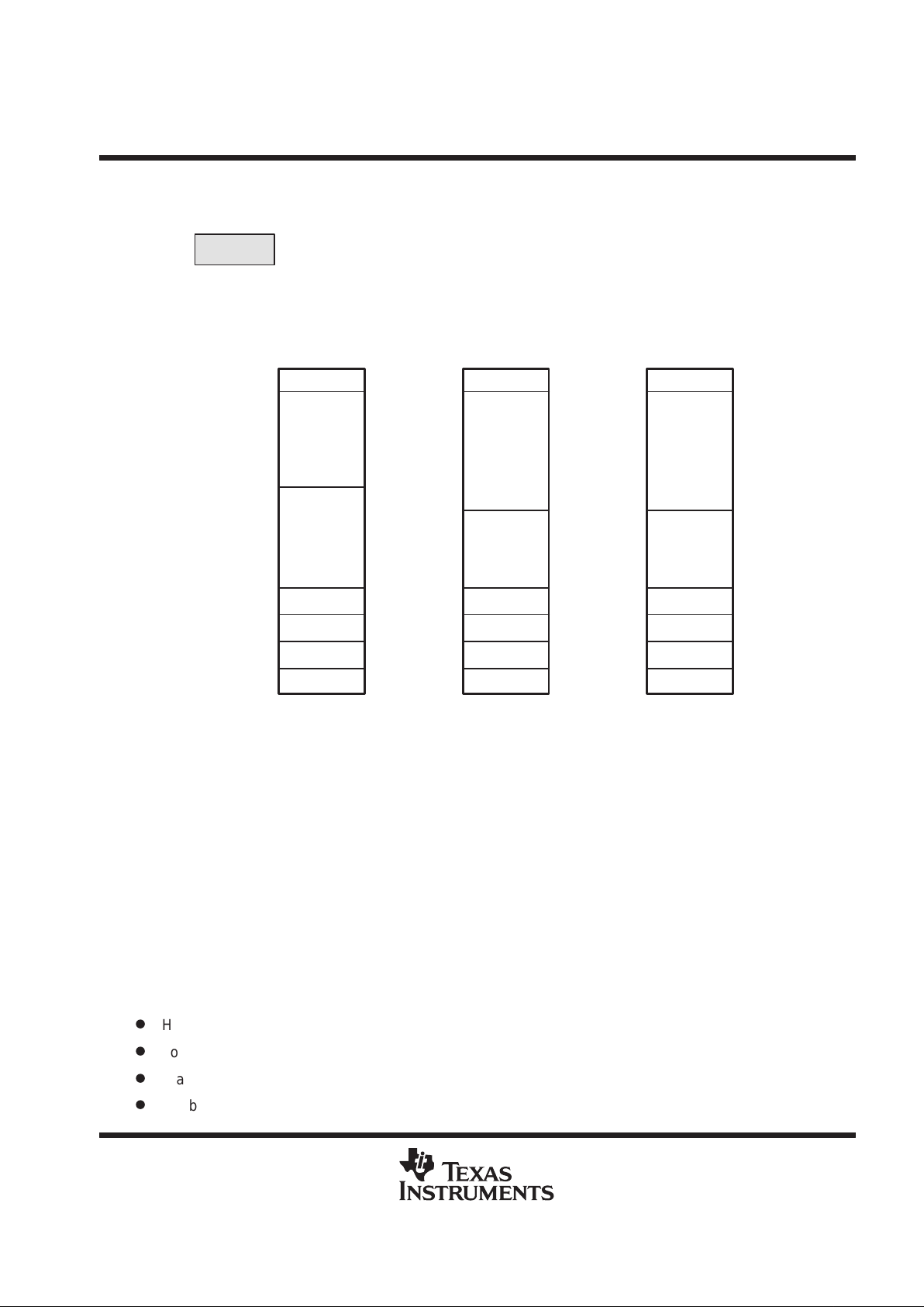
NC
S22/O22
S21/O21
S19/O19
S17/O17
S16/O16
S15/O15
S14/O14
S13/O13
S12/O12
S11/O11
S10/O10
S9/O9
S7/07
S8/O8
S4/O4
S3/O3
S2/O2
S1
S0
COM0
TP0.0
TP0.1
TP0.2
TP0.3
TP0.4
TP0.5
P0.0
P0.2/TXD
P0.3
P0.5
P0.6
P0.7
P1.0
P1.1
P1.2
P1.3
P1.4
P1.6
P1.7
Xin
Xout/TCLK
RST/NMI
TCK
TMS
TDI/VPP
TDO/TDI
R13
S27/O27
S26/O26
S25/O25
S24/O24
S23/O23
P2.3
P2.4
P2.5
P2.6
P2.7
P3.0
P3.1
P3.3/TA0
P3.4/TA1
P3.6/TA3
P3.7/TA4
P4.0
P4.1
P4.2/STE
P4.4/SOMI
P4.5/UCLK
V
SS3
P4.3/SIMO
PJM or HFD PACKAGE
(TOP VIEW)
CIN
S29/O29/CMPI
R33
R23
S20/O20
S5/O5
P3.5/TA2
P0.1/RXD
P1.5
26
27
28
29
30
55
54
53
52
51
P2.1
P2.2
NC
COM1
COM2
COM3
P4.7/URXD
S28/O28
XBUF
V
CC1
P0.4
P2.0
V
SS2
V
CC2
P3.2/TACLK
P4.6/UTXD
S18/O18
S6/O6
SS1
V
R03
NC – No internal connection
Copyright 1998, Texas Instruments Incorporated
MSP430x33x
MIXED SIGNAL MICROCONTROLLER
SLAS163 – FEBRUARY 1998
Template Release Date: 7–11–94
2
POST OFFICE BOX 655303 DALLAS, TEXAS 75265
•
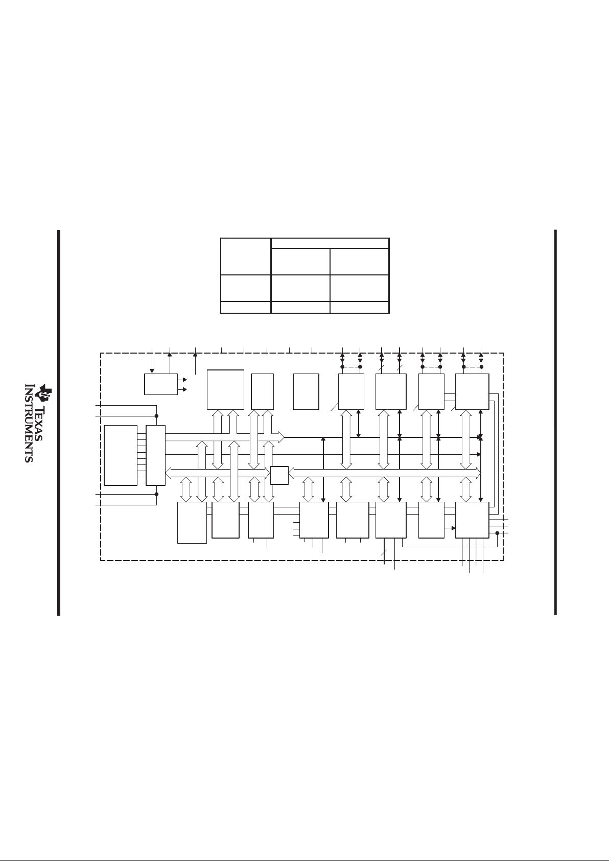
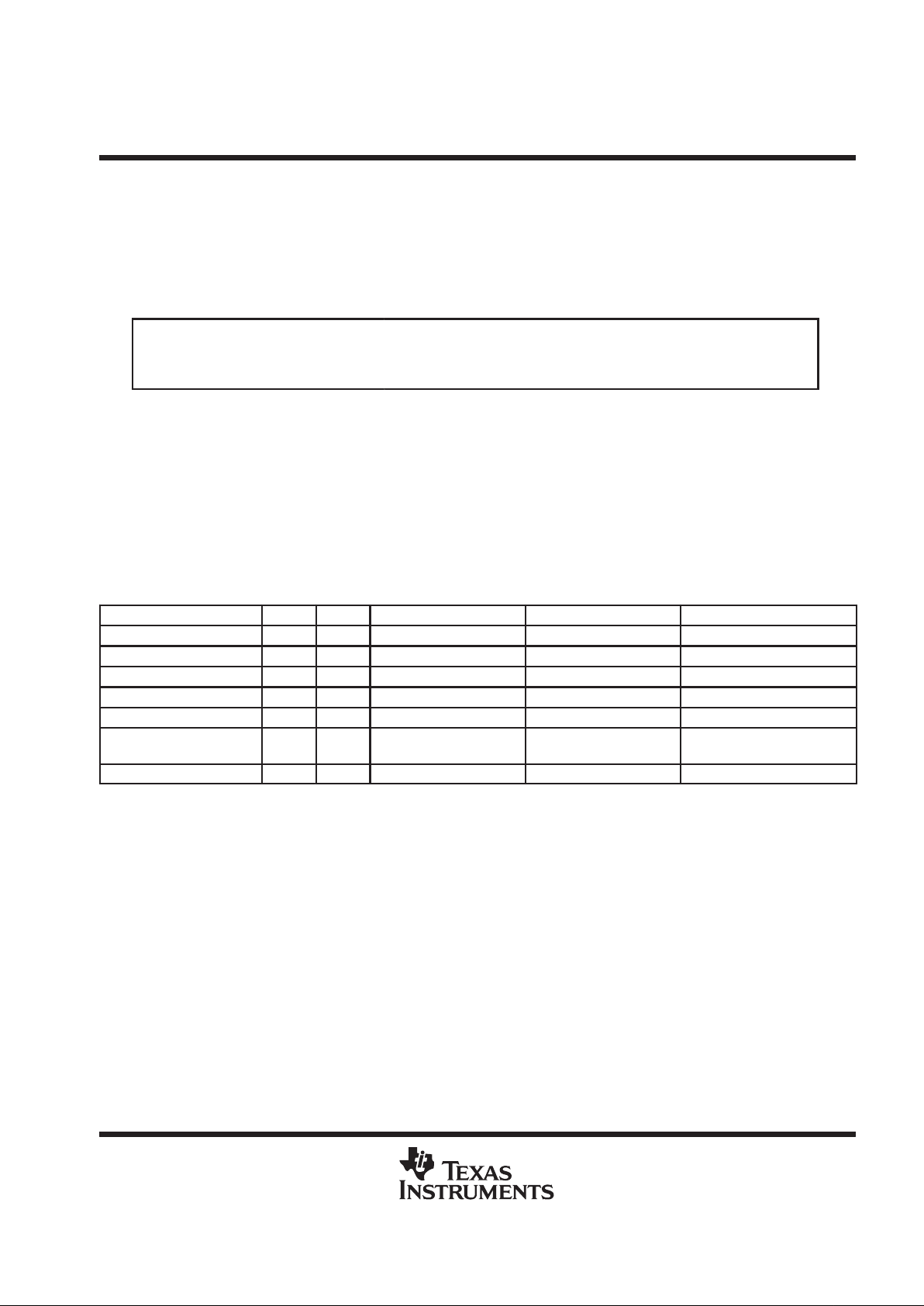
AVAILABLE OPTIONS
PACKAGED DEVICES
T
A
PLASTIC
QFP
(PJM)
CERAMIC
QFP
(HFD)
°
°
MSP430C336IPJM
–
40°C to 85°C
MSP430C337IPJM
MSP430P337IPJM
—
°
25°C
—
PMS430E337HFD
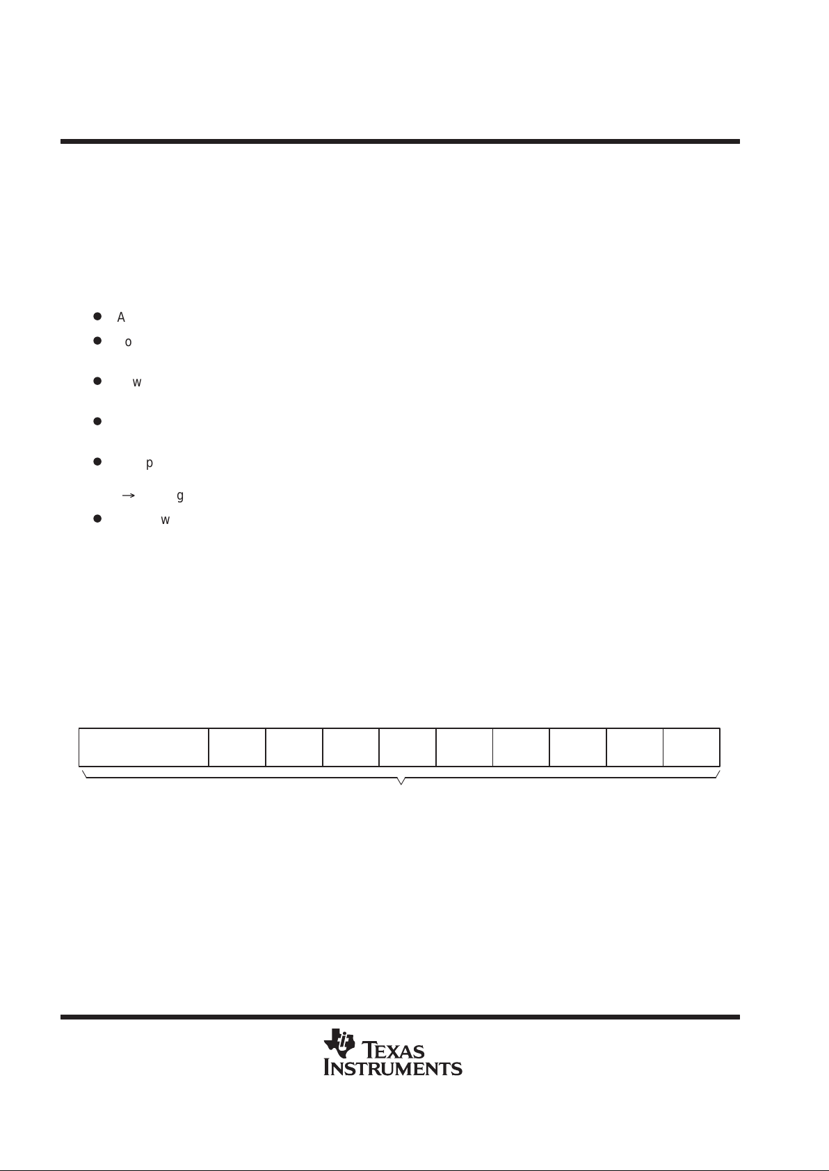
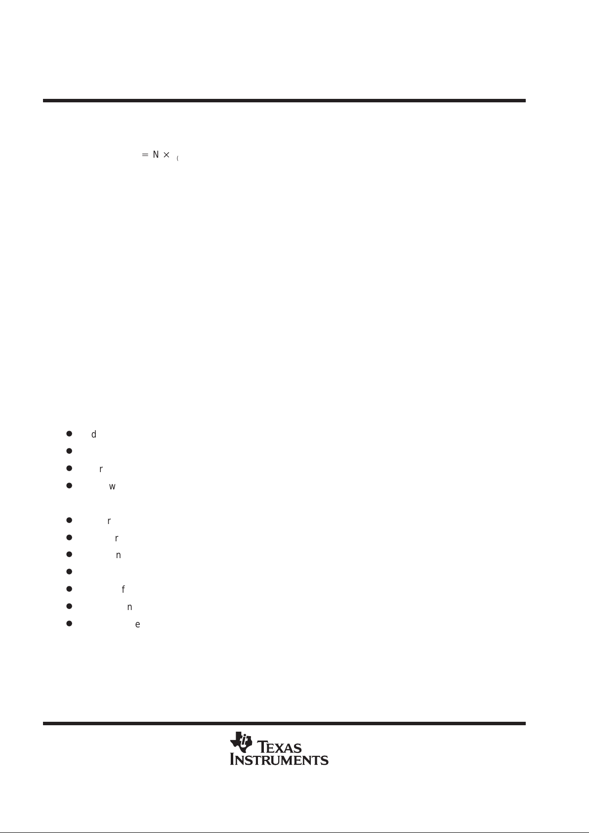
functional block diagram
Oscillator
FLL
System Clock
ACLK
MCLK
24/32 kB ROM
32 kB OPT or
1024B
RAM
SRAM
Power-on-
Reset
I/O Port
1x8 Digital
I/O’s
I/O Port
2x8 I/O’s All
Interr. Cap.
8 8
2 Int. Vectors
I/O Port
1x8 Digital
I/O’s
I/O Port
8 I/O’s, All With
Interr. Cap.
3 Int. Vectors
CPU
Incl. 16 Reg.
Test
JTAG
Bus
Conv
USART
UART or
8 Bit Timer/Port
Applications
Timer, O/P
Basic
LCD
120 Segments
1, 2, 3, 4 MUX
SPI Function
Timer/Counter
Timer1
MPY
Watchdog TimerA
MPYS
timer
MAC
16x16 Bit
8x8 Bit
15/16 Bit
16 Bit
PWM
MAB, 16 Bit
MDB, 16 Bit
MAB, 4 Bit
MDB, 8 Bit
MCB
TACLK
TA0–4
UTXD
URXD
UCLK
STE
SIMO
SOMI
TXD RXD
6
LCD
f
CMPI
TP0.0–0.5
CIN
XIN XOut XBUF
V
CC1VCC2VSS1VSS2
RST/NMI P4.0 P4.7 P2.x P1.x P3.0 P3.7 P0.0 P0.7
Com0–3
S0–28/O2–28
S29/O29/CMPI
R03
R13
R23
R33
TDI
TDO
TMS
TCK
USART TimerA RXD,
TXD
A/D Conv.
EPROM
C: ROM
P: OTP
E: EPROM
Multiplier
MSP430x33x
MIXED SIGNAL MICROCONTROLLERS
SLAS163 – FEBRUARY 1998
3
POST OFFICE BOX 655303 • DALLAS, TEXAS 75265
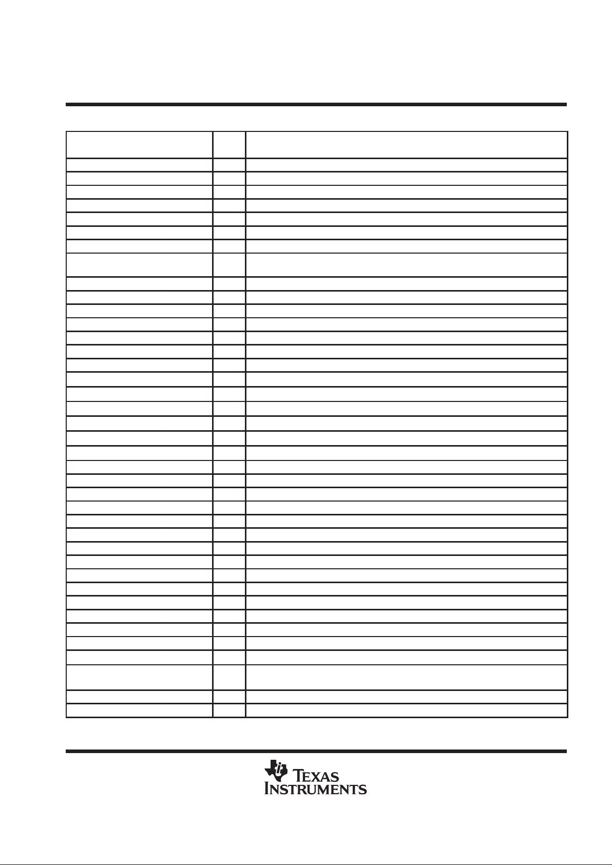
Terminal Functions
TERMINAL
NAME NO.
I/O
DESCRIPTION
CIN 2 I Input port. CIN is used as an enable for counter TPCNT1 – timer/port
COM0–3 56–53 O Common outputs. COMM0-3 are used for LCD backplanes – LCD
P0.0 9 I/O General purpose digital I/O
P0.1/RXD 10 I/O General purpose digital I/O, receive digital Input port – 8-bit timer/counter
P0.2/TXD 11 I/O General purpose digital I/O, transmit data output port – 8-bit timer/counter
P0.3–P0.7 12–16 I/O Five general purpose digital I/Os, bit 3-7
P1.0–P1.7 17–24 I/O Eight general purpose digital I/Os, bit 0-7
P2.0–P2.7 25–27,
31–35
I/O Eight general purpose digital I/Os, bit 0-7
P3.0, P3.1 36,37 I/O Two general purpose digital I/Os, bit 0 and bit 1
P3.2/TACLK 38 I/O General purpose digital I/O, clock input – timer A
P3.3/TA0 39 I/O General purpose digital I/O, capture I/O, or PWM output port – Timer_A CCR0
P3.4/TA1 40 I/O General purpose digital I/O, capture I/O, or PWM output port – Timer_A CCR1
P3.5/TA2 41 I/O General purpose digital I/O, capture I/O, or PWM output port – Timer_A CCR2
P3.6/TA3 42 I/O General purpose digital I/O, capture I/O, or PWM output port – Timer_A CCR3
P3.7/TA4 43 I/O General purpose digital I/O, capture I/O, or PWM output port – Timer_A CCR4
P4.0 44 I/O General purpose digital I/O, bit 0
P4.1 45 I/O General purpose digital I/O, bit 1
P4.2/STE 46 I/O General purpose digital I/O, slave transmit enable – USART/SPI mode
P4.3/SIMO 47 I/O General purpose digital I/O, slave in/master out – USART/SPI mode
P4.4/SOMI 48 I/O General purpose digital I/O, master in/slave out – USART/SPI mode
P4.5/UCLK 49 I/O General purpose digital I/O, external clock input – USART
P4.6/UTXD 50 I/O General purpose digital I/O, transmit data out – USART/UART mode
P4.7/URXD 51 I/O General purpose digital I/O, receive data in – USART/UART mode
R03 88 I Input port of fourth positive (lowest) analog LCD level (V5) – LCD
R13 89 I Input port of third most positive analog LCD level (V3 of V4) – LCD
R23 90 I Input port of second most positive analog LCD level (V2) – LCD
R33 91 O Output of most positive analog LCD level (V1) – LCD
RST/NMI 96 I Reset input or non-maskable interrupt input port
S0 57 O Segment line S0 – LCD
S1 58 O Segment line S1 – LCD
S2/O2–S5/O5 59–62 O Segment lines S2 to S5 or digital output ports, O2-O5, group 1 – LCD
S6/O6–S9/O9 63–66 O Segment lines S6 to S9 or digital output ports O6-O9, group 2 – LCD
S10/O10–S13/O13 67–70 O Segment lines S10 to S13 or digital output ports O10-O13, group 3 – LCD
S14/O14–S17/O17 71–74 O Segment lines S14 to S17 or digital output ports O14-O17, group 4 – LCD
S18/O18–S21/O21 75–78 O Segment lines S18 to S21 or digital output ports O18-O21, group 5 – LCD
S22/O22–S25/O25 79, 81–83 O Segment line S22 to S25 or digital output ports O22-O25, group 6 – LCD
S26/O26–S29/O29/CMPI 84–87 O Segment line S26 to S29 or digital output ports O26-O29, group 7 – LCD. Segment line S29
can be used as comparator input port CMPI – timer/port
TCK 95 I Test clock. TCK is the clock input port for device programming and test
TDI/VPP 93 I Test data input. TDI/VPP is used as a data input port or input for programming voltage
MSP430x33x
MIXED SIGNAL MICROCONTROLLERS
SLAS163 – FEBRUARY 1998
4
POST OFFICE BOX 655303 • DALLAS, TEXAS 75265
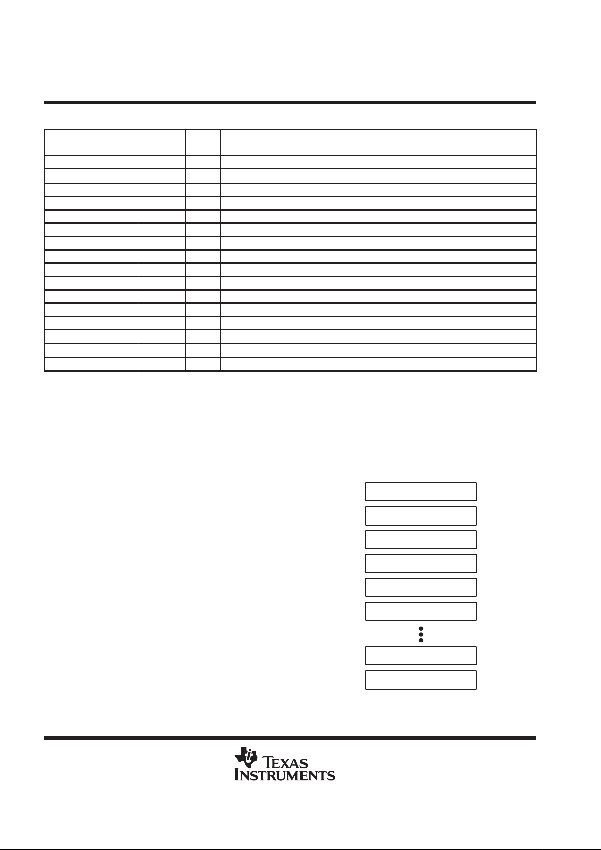
Terminal Functions
TERMINAL
NAME NO.
I/O
DESCRIPTION
TMS 94 I Test mode select. TMS is used as an input port for device programming and test
TDO/TDI 92 I/O Test data output port. TDO/TDI data output or programming data input terminal
TP0.0 3 O General purpose 3–state digital output port, bit 0 – timer/port
TP0.1 4 O General purpose 3–state digital output port, bit 1 – timer/port
TP0.2 5 O General purpose 3–state digital output port, bit 2 – timer/port
TP0.3 6 O General purpose 3–state digital output port, bit 3 – timer/port
TP0.4 7 O General purpose 3–state digital output port, bit 4 – timer/port
TP0.5 8 I/O General purpose 3–state digital input/output port, bit 5 – timer/port
VCC1 1 Positive supply voltage
VCC2 29 Positive supply voltage
VSS1 100 Ground reference
VSS2 28 Ground reference
VSS3 52 Ground reference
XBUF 97 O System clock (MCLK) or crystal clock (ACLK) output
Xin 99 I Input port for crystal oscillator
Xout/TCLK 98 I/O Output terminal of crystal oscillator or test clock input
short-form description
processing unit
The processing unit is based on a consistent and orthogonal designed CPU and instruction set. This design
structure results in a RISC-like architecture, highly transparent to the application development and is
distinguished due to ease of programming. All operations, other than program-flow instructions consequently
are performed as register operations in conjunction with seven addressing modes for source and four modes
for destination operand.
cpu registers
Sixteen registers are located inside the CPU,
providing reduced instruction execution time. This
reduces a register-register operation execution
time to one cycle of the processor frequency.
Four of the registers are reserved for special use
as a program counter, a stack pointer, a status
register and a constant generator. The remaining
registers are available as general purpose
registers.
Peripherals are connected to the CPU using a
data address and control bus and can be handled
easily with all instructions for memory manipulation.
Program Counter
General Purpose Register
PC/R0
Stack Pointer
SP/R1
Status Register
SR/CG1/R2
Constant Generator
CG2/R3
R4
General Purpose Register
R5
General Purpose Register R14
General Purpose Register
R15
MSP430x33x
MIXED SIGNAL MICROCONTROLLERS
SLAS163 – FEBRUARY 1998
5
POST OFFICE BOX 655303 • DALLAS, TEXAS 75265
instruction set
The instruction set for this register-register architecture provides a powerful and easy-to-use assembly
language. The instruction set consists of 52 instructions, with three formats and seven addressing modes.
T able 1 provides a summation and example of the three types of instruction formats; the addressing modes are
listed in Table 2.
Table 1. Instruction Word Formats
Dual operands, source–destination e.g. ADD R4,R5 R4 + R5 → R5
Single operands, destination only e.g. CALL R8 PC → (TOS), SR → (TOS), R8→ PC
Relative jump, un–/conditional e.g. JNE Jump-on equal bit = 0
Instructions that can operate on both word and byte data are differentiated by the suffix ’.B’ when a byte
operation is required.
Examples: Instructions for word operation: Instructions for byte operation:
MOV ede,toni MOV.B ede,toni
ADD #235h,&MEM ADD.B #35h,&MEM
PUSH R5 PUSH.B R5
SWPB R5 –––
Table 2. Address Mode Descriptions
ADDRESS MODE S D SYNTAX EXAMPLE OPERATION
register √ √ MOV Rs,Rd MOV R10,R11 R10 → R11
indexed √ √ MOV X(Rn),Y(Rm) MOV 2(R5),6(R6) M(2+R5) → M(6+R6)
symbolic (PC relative) √ √ MOV EDE,TONI M(EDE) → M(TONI)
absolute √ √ MOV &MEM,&TCDAT M(MEM) → M(TCDAT)
indirect √ MOV @Rn,Y(Rm) MOV @R10,Tab(R6) M(R10) → M(Tab+R6)
indirect autoincrement √ MOV @Rn+,Rm MOV @R10+,R11 M(R10) → R11
R10 + 2
→ R10
immediate √ MOV #X,T ONI MOV #45,TONI #45 → M(TONI)
NOTE 1: S = source, D = destination.
Computed branches (BR) and subroutine calls (CALL) instructions use the same addressing modes as the other
instructions. These addressing modes provide
indirect
addressing, ideally suited for computed branches and
calls. The full use of this programming capability permits a program structure different from conventional 8- and
16-bit controllers. For example, numerous routines can easily be designed to deal with pointers and stacks
instead of using Flag type programs for flow control.
MSP430x33x
MIXED SIGNAL MICROCONTROLLERS
SLAS163 – FEBRUARY 1998
6
POST OFFICE BOX 655303 • DALLAS, TEXAS 75265
operation modes and interrupts
The MSP430 operating modes support various advanced requirements for ultra-low power and ultra-low energy
consumption. This is achieved by the intelligent management of the operations during the different module
operation modes and CPU states. The requirements are fully supported during interrupt event handling. An
interrupt event awakens the system from each of the various operating modes and returns with the RETI
instruction to the mode that was selected before the interrupt event. The clocks used are ACLK and MCLK.
ACLK is the crystal frequency and MCLK is a multiple of ACLK and is used as the system clock.
The following five operating modes are supported:
D
Active mode (AM). The CPU is enabled with different combinations of active peripheral modules.
D
Low power mode 0 (LPM0). The CPU is disabled, peripheral operation continues, ACLK and MCLK signals
are active, and loop control for MCLK is active.
D
Low power mode 1 (LPM1). The CPU is disabled, peripheral operation continues, ACLK and MCLK signals
are active, and loop control for MCLK is inactive.
D
Low power mode 2 (LMP2). The CPU is disabled, peripheral operation continues, ACLK signal is active,
and MCLK and loop control for MCLK are inactive.
D
Low power mode 3 (LMP3). The CPU is disabled, peripheral operation continues, ACLK signal is active,
MCLK and loop control for MCLK are inactive, and the dc generator for the digital controlled oscillator (DCO)
(³MCLK generator) is switched off.
D
Low power mode 4 (LMP4). The CPU is disabled, peripheral operation continues, ACLK signal is inactive
(crystal oscillator stopped), MCLK and loop control for MCLK are inactive, and the dc generator for the DCO
is switched off.
The special function registers (SFR) include module-enable bits that stop or enable the operation of the specific
peripheral module. All registers of the peripherals may be accessed if the operational function is stopped or
enabled. However, some peripheral current-saving functions are accessed through the state of local register
bits. An example is the enable/disable of the analog voltage generator in the LCD peripheral which is turned
on or off using one register bit.
The most general bits that influence current consumption and support fast turn-on from low power operating
modes are located in the status register (SR). Four of these bits control the CPU and the system clock generator:
SCG1, SCG0, OscOff, and CPUOff.
Reserved For Future
Enhancements
15 9 8 7 0
V SCG1 SCG0 OscOff CPUOff GIE N Z C
rw-0
interrupts
Software determines the activation of interrupts through the monitoring of hardware set interrupt flag status bits,
the control of specific interrupt enable bits in SRs, the establishment of interrupt vectors, and the programming
of interrupt handlers. The interrupt vectors and the power-up starting address are located in ROM address
locations 0FFFFh through 0FFE0h. Each vector contains the 16-bit address of the appropriate interrupt handler
instruction sequence. Table 3 provides a summation of interrupt functions and addresses.
MSP430x33x
MIXED SIGNAL MICROCONTROLLERS
SLAS163 – FEBRUARY 1998
7
POST OFFICE BOX 655303 • DALLAS, TEXAS 75265
Table 3. Interrupt Functions and Addresses
INTERRUPT SOURCE INTERRUPT FLAG SYSTEM INTERRUPT WORD ADDRESS PRIORITY
Power-up, external reset, Watchdog WDTIFG Reset 0FFFEh 15, highest
NMI,
Oscillator fault
NMIIFG (see Note 2)
OFIFG (see Note 2)
non-maskable
(non)-maskable
0FFFCh 14
Dedicated I/O P0IFG.0 maskable 0FFFAh 13
Dedicated I/O P0IFG.1 maskable 0FFF8h 12
maskable 0FFF6h 11
Watchdog timer WDTIFG maskable 0FFF4h 10
Timer_A CCIFG0 (see Note 3) maskable 0FFF2h 9
Timer_A TAIFG (see Note 3) maskable 0FFF0h 8
UART Receive URXIFG maskable 0FFEEh 7
UART Transmit UTXIFG maskable 0FFECh 6
0FFEAh 5
Timer/Port See Note 3 maskable 0FFE8h 4
I/O Port P2 P2IFG.07 (see Note 2) maskable 0FFE6h 3
I/O Port P1 P1IFG.07 (see Note 2) maskable 0FFE4h 2
Basic Timer BTIFG maskable 0FFE2h 1
I/O Port P0 P0IFG.27 (see Note 2) maskable 0FFE0h 0, lowest
NOTES: 2. Multiple source flags
3. Interrupt flags are located in the module
special function registers
Most interrupt and module enable bits are collected into the lowest address space. Special function register bits
that are not allocated to a functional purpose are not physically present in the device. Simple SW access is
provided with this arrangement.
interrupt enable 1 and 2
7654 0
P0IE.1 OFIE WDTIE
321
P0IE.0
rw-0 rw-0 rw-0 rw-0
Address
0h
WDTIE: Watchdog timer interrupt enable signal
OFIE: Oscillator fault interrupt enable signal
P0IE.0: Dedicated I/O P0.0 interrupt enable signal
P0IE.1: P0.1 or 8-bit timer/counter, RXD interrupt enable signal
7654 0
TPIE UTXIE URXIE
rw-0
321
rw-0 rw-0 rw-0
Address
01h BTIE
URXIE: USART receive interrupt enable signal
UTXIE: USART transmit interrupt enable signal
TPIE: Timer/Port interrupt enable signal
BTIE: Basic Timer interrupt enable signal
MSP430x33x
MIXED SIGNAL MICROCONTROLLERS
SLAS163 – FEBRUARY 1998
8
POST OFFICE BOX 655303 • DALLAS, TEXAS 75265
interrupt flag registers 1 and 2
7654 0
P0IFG.1 OFIFG WDTIFG
321
rw-0 rw-1 rw-0
Address
02h NMIIFG P0IFG.0
rw-0 rw-0
WDTIFG: Set on overflow or security key violation
or
Reset on VCC1 power-on or reset condition at ’RST/NMI-pin
OFIFG: Flag set on oscillator fault
P0.0IFG: Dedicated I/O P0.0
P0.1IFG: P0.1 or 8-bit timer/counter, RXD
NMIIFG: Signal at ’RST/NMI-pin
7654 0
UTXIFG URXIFG
rw
321
rw-1 rw-0
Address
03h BTIFG
URXIFG: USART receive flag
UTXIFG: USART transmit flag
BTIFG: Basic Timer flag
module enable registers 1 and 2
7654 0321
Address
04h
7654 0
UTXE URXE
321
rw-0 rw-0
Address
05h
UTXE: USART transmit enable
URXE: USART receive enable
MSP430x33x
MIXED SIGNAL MICROCONTROLLERS
SLAS163 – FEBRUARY 1998
9
POST OFFICE BOX 655303 • DALLAS, TEXAS 75265
module enable registers 1 and 2 (continued)
Legend rw:
rw-0:
Bit can be read and written
Bit can be read and written. It is reset by PUC
SFR bit not present in device
ROM memory organization
Int. Vector
24 kB ROM
1024B RAM
16b Per.
8b Per.
SFR
FFFFh
FFE0h
FFDFh
A000h
05FFh
0200h
01FFh
0100h
00FFh
0010h
000Fh
0000h
MSP430C336
Int. Vector
32 kB ROM
1024B RAM
16b Per.
8b Per.
SFR
FFFFh
FFE0h
FFDFh
8000h
05FFh
0200h
01FFh
0100h
00FFh
0010h
000Fh
0000h
MSP430C337
Int. Vector
32 kB OTP
or
EPROM
1024B RAM
16b Per.
8b Per.
SFR
FFFFh
FFE0h
FFDFh
8000h
05FFh
0200h
01FFh
0100h
00FFh
0010h
000Fh
0000h
MSP430P337
PMS430E337
peripherals
Peripherals are connected to the CPU through a data, address, and control bus and can be handled easily with
instructions for memory manipulation.
oscillator and system clock
Two clocks are used in the system, the system (master) clock (MCLK) and the auxiliary clock (ACLK). The MCLK
is a multiple of the ACLK. The ACLK runs with the crystal oscillator frequency. The special design of the oscillator
supports the feature of low current consumption and the use of a 32 768 Hz crystal. The crystal is connected
across two terminals without any other external components being required.
The oscillator starts after applying VCC, due to a reset of the control bit (OscOff) in the status register (SR). It
can be stopped by setting the OscOff bit to a 1. The enabled clock signals ACLK, ACLK/2, ACLK/4, OR MCLK
are accessible for use by external devices at output terminal XBUF .
The controller system clocks have to deal with different requirements according to the application and system
condition. Requirements include:
D
High frequency in order to react quickly to system hardware requests or events
D
Low frequency in order to minimize current consumption, EMI, etc.
D
Stable frequency for timer applications e.g. real time clock (RTC)
D
Enable start-stop operation with minimum delay to operation function.
MSP430x33x
MIXED SIGNAL MICROCONTROLLERS
SLAS163 – FEBRUARY 1998
10
POST OFFICE BOX 655303 • DALLAS, TEXAS 75265
These requirements cannot all be met with fast frequency high-Q crystals or with RC-type low-Q oscillators. The
compromise selected for the MSP430 uses a low-crystal frequency which is multiplied to achieve the desired
nominal operating range:
f
(system)
+N
f
(crystal)
The crystal frequency multiplication is acheived with a frequency locked loop (FLL) technique. The factor N is
recommended to be 32, 64, 96, or 128 depending on the maximum clock frequency and the electrical
characteristics provided by this datasheet. The FLL technique, in combination with a digital controlled oscillator
(DCO) provides immediate start-up capability together with long term crystal stability . The frequency variation
of the DCO with the FLL inactive is typically 330 ppm which means that with a cycle time of 1 µs the maximum
possible variation is 0.33 ns. For more precise timing, the FLL can be used which forces longer cycle times if
the previous cycle time was shorter than the selected one. This switching of cycle times makes it possible to
meet the chosen system frequency over a long period of time.
The start-up operation of the system clock depends on the previous machine state. During a PUC, the DCO
is reset to its lowest possible frequency . The control logic starts operation immediately after recognition of PUC.
multiplication
The multiplication operation is supported by a dedicated peripheral module. The module performs 16x16, 16x8,
8x16, and 8x8 bit operations. The module is capable of supporting signed and unsigned multiplication as well
as unsigned multiply and accumulate operations. The result of an operation can be accessed immediately after
the operands have been loaded into the peripheral registers. No additional clock cycles are required.
digital I/O
Five eight-bit I/O ports (P0 thru P4) are implemented. Port P0 has six control registers, P1 and P2 have seven
control registers, and P3 and P4 modules have four control registers to give maximum flexibility of digital
input/output to the application:
D
Individual I/O bits are independently programable.
D
Any combination of input, output, and interrupt conditions is possible.
D
Interrupt processing of external events is fully implemented for all eight bits of the P0, P1, and P2 ports.
D
Read/write access is available to all registers by all instructions.
The seven registers are:
D
Input register contains information at the pins
D
Output register contains output information
D
Direction register controls direction
D
Interrupt edge select contains input signal change necessary for interrupt
D
Interrupt flags indicates if interrupt(s) are pending
D
Interrupt enable contains interrupt enable pins
D
Function select determines if pin(s) used by module or port
These registers contain eight bits each with the exception of the the interrupt flag register and the interrupt
enable register which are 6 bits each. The two least significant bit (LSBs) of the interrupt flag and enable
registers are located in the special function register (SFR). Five interrupt vectors are implemented, one for Port
P0.0, one for Port P0.1, one commonly used for any interrupt event on Port P0.2 to Port P0.7, one commonly
used for any interrupt event on Port P1.0 to Port P1.7, and one commonly used for any interrupt event on Port
P2.0 to Port P2.7.

MSP430x33x
MIXED SIGNAL MICROCONTROLLERS
SLAS163 – FEBRUARY 1998
11
POST OFFICE BOX 655303 • DALLAS, TEXAS 75265
LCD drive
Liquid crystal displays (LCDs) for static, 2-, 3-, and 4-MUX operation can be driven directly. The operation of
the controller LCD logic is defined by software through memory-bit manipulation. LCD memory is part of the LCD
module, not part of data memory . Eight mode and control bits define the operation and current consumption of
the LCD drive. The information for the individual digits can be easily obtained using table programming
techniques combined with the proper addressing mode. The segment information is stored into LCD memory
using instructions for memory manipulation.
The drive capability is defined by the external resistor divider that supports analog levels for 2-, 3-, and 4-MUX
operation. Groups of the LCD segment lines can be selected for digital output signals. The MSP430x33x
configuration has four common lines, 30 segment lines, and four terminals for adjusting the analog levels.
basic timer1
The Basic Timer1 (BT1) divides the frequency of MCLK or ACLK, as selected with the SSEL bit, to provide low
frequency control signals. This is done within the system by one central divider, the basic timer, to support low
current applications. The BTCTL control register contains the flags which control or select the different
operational functions. When the supply voltage is applied or when a reset of the device (RST/NMI pin), a
watchdog overflow, or a watchdog security key violation occurrs, all bits in the register hold undefined or
unchanged status. The user software usually configures the operational conditions on the BT during
initialization.
The basic timer has two eight bit timers which can be cascaded to a sixteen bit timer. Both timers can be read
and written by software. Two bits in the SFR address range handle the system control interaction according to
the function implemented in the basic timer. These two bits are the Basic T imer Interrupt Flag (BTIFG) and the
Basic Timer Interrupt Enable (BTIE) bit.
watchdog timer
The primary function of the Watchdog T imer (WDT) module is to perform a controlled system restart after a S/W
upset has occurred. If the selected time interval expires, a system reset is generated. If this watchdog function
is not needed in an application, the module can work as an interval timer, which generates an interrupt after the
selected time interval.
The watchdog timer counter (WDTCNT) is a 15/16-bit upcounter which is not directly accessible by software.
The WDTCNT is controlled using the watchdog timer control register (WDTCTL), which is an 8-bit read/write
register. W riting to WDTCTL, in both operating modes (watchdog or timer) is only possible by using the correct
password in the high-byte. The low-byte stores data written to the WDTCTL. The high-byte password is 05Ah.
If any value other than 05Ah is written to the high-byte of the WDTCTL, a system reset PUC is generated.
When
the password is read its value is 069h that minimizes accidental write operations to the WDTCTL register.
A
read-access to WDTCTL is only possible by writing 05Ah as the password in the high-byte of the WDTCTL. This
avoids an accidental write-access on the WDTCTL. Additionally to the watchdog timer control bits, there are
two bits included in the WDTCTL that configure the NMI pin.
USART
The universal synchronous/asynchronous interface is a dedicated peripheral module which provides serial
communications. The USART supports synchronous SPI (3 or 4 pin), and asynchronous UART
communications protocols, using double buffered transmit and receive channels. Data streams of 7 or 8 bits
in length can be transferred at a rate determined by the program, or by a rate defined by an external clock. Low
power applications are optimized by UART mode options which allow for the receipt of only the first byte of a
complete frame. The applications software then decides if the succeeding data is to be processed. This option
reduces power consumption.
Two dedicated interrupt vectors are assigned to the USAR T module, one for the receive and one for the transmit
channel.

MSP430x33x
MIXED SIGNAL MICROCONTROLLERS
SLAS163 – FEBRUARY 1998
12
POST OFFICE BOX 655303 • DALLAS, TEXAS 75265
timer/port
The timer/port module has two 8-bit counters, an input that triggers one counter and six digital outputs with
3-state capability . Both counters have an independent clock selector for selecting an external signal or one of
the internal clocks (ACLK or MCLK). One of the counters has an extended control capability to halt, count
continuously , or gate the counter by selecting one of two external signals. This gate signal sets the interrupt flag
if an external signal is selected and the gate stops the counter.
Both timers can be read to and written from by software. The two 8-bit counters can be cascaded to form a 16-bit
counter. A common interrupt vector is implemented. The interrupt flag can be set by three events in the 8-bit
counter mode (gate signal or overflow from the counters) or by two events in the 16-bit counter mode (gate signal
or overflow from the MSB of the cascaded counter).
slope A/D conversion
Slope A/D conversion is accomplished with the timer/port module using external resistor(s) for reference (R
ref
),
external resistor(s) to the measured (R
meas
), and an external capacitor. The external components are driven
by software in such a way that the internal counter measures the time that is needed to charge or discharge
the capacitor.The reference resistor’s (R
ref
) charge or discharge time is represented by N
ref
counts. The
unknown resistors (R
meas
) charge or discharge time is represented by N
meas
counts. The unknown resistor’s
value R
meas
is the value of R
ref
multiplied by the relative number of counts (N
meas/Nref
). This value determines
resistive sensor values that corresponds to the physical data, for example temperature, when an NTC or PTC
resistor is used.
timer_a
The timer_a module offers one sixteen bit counter and five capture/compare registers. The timer clock source
can be selected to come from an external source T ACLK (SSEL=0), the ACLK (SSEL=1), or MCLK (SSEL=2
or SSEL=3). The clock source can be divided by one, two, four or eight. The timer can be fully controlled (in word
mode) since it can be halted, read, and written. It can be stopped, run continuously , count up, or count up/down
using one compare block to determine the period. The five capture/compare blocks are configured by the
application software to run in either capture or compare mode.
The capture mode is primarily used to measure external or internal events with any combination of positive,
negative, or both edges of the clock. The clock can also be stopped in capture mode by software. One external
event (CCISx=0) per capture block can be selected. If CCISx=1, the ACLK is the capture signal; and if CCISx=2
or CCISx=3, software capture is chosen.
The compare mode is primarily used to generate timing for the software or application hardware or to generate
pulse-width modulated output signals for various purposes like D/A conversion functions or motor control. An
individual output module, which can run independently of the compare function or is triggered in several ways,
is assigned to each of the five capture/compare registers.
Two interrupt vectors are used by the timer_a module. One individual vector is assigned to capture/compare
block CCR0 and one common interrupt vector is assigned to the timer and the other four capture/compare
blocks. The five interrupt events using the common vector are identified by an individual interrupt vector word.
The interrupt vector word is used to add an offset to the program counter to continue the interrupt handler
software at the correct location. This simplifies the interrupt handler and gives each interrupt event the same
interrupt handler overhead of 5 cycles.

MSP430x33x
MIXED SIGNAL MICROCONTROLLERS
SLAS163 – FEBRUARY 1998
13
POST OFFICE BOX 655303 • DALLAS, TEXAS 75265
8-bit timer/counter
The 8-bit interval timer supports three major functions for applications:
D
Serial communication or data exchange
D
Plus counting or plus accumulation
D
Timer
8-bit timer/counter (continued)
The 8-bit timer/counter peripheral includes the following major blocks: an 8-bit Up-Counter with preload register,
an 8-bit Control Register, an Input clock selector, an Edge detection (e.g. Start bit detection for asynchronous
protocols), and an input and output data latch, triggered by the carry-out-signal from the 8-bit counter.
The 8-bit counter counts up with an input clock which is selected by two control bits from the control register.
The four possible clock sources are MCLK, ACLK, the external signal from terminal P0.1, and the signal from
the logical .AND. of MCLK and terminal P0.1.
Two counter inputs (load, enable) control the counter operation. The load input controls load operations. A
write-access to the counter results in loading the content of the preload register into the counter. The software
writes or reads the preload register with all instructions. The preload register acts as a buffer and can be written
immediately after the load of the counter is completed. The enable input enables the count operation. When
the enable signal is set to high, the counter will count-up each time a positive clock edge is applied to the clock
input of the counter.

MSP430x33x
MIXED SIGNAL MICROCONTROLLERS
SLAS163 – FEBRUARY 1998
14
POST OFFICE BOX 655303 • DALLAS, TEXAS 75265
peripheral file map
Peripherals with byte access
UART Transmit Buffer , UTXBUF 077h Port P3 Port P3 Selection, P3SEL 01Bh
Receive Buffer, URXBUF 076h Port P3 Direction, P3DIR 01Ah
Baud Rate, UBR1 075h Port P3 Output, P3OUT 019h
Baud Rate, UBR0 074h Port P3 Input, P3IN 018h
Modulation Control, UMCTL 073h Port P0 Port P0 Interrupt Enable, P0IE 015h
Receive Control, URCTL 072h Port P0 Interrupt Edge Select, P0IES 014h
Transmit Control, UTCTL 071h Port P0 Interrupt Flag, P0IFG 013h
UART Control, UCTL 070h Port P0 Direction, P0DIR 012h
EPROM EPROM Control, EPCTL 054h Port P0 Output, P0OUT 011h
Crystal Buffer Crystal Buffer Control, CBCTL 053h Port P0 Input, P0IN 010h
System Clock SCG Frequency Control, SCFQCTL 052h Special SFR Interrupt Flag2, IFG2 003h
SCG Frequency Integrator, SCFI1 051h Function SFR Interrupt Flag1, IFG1 002h
SCG Frequency Integrator, SCFI0 050h SFR Interrupt Enable2, IE2 001h
Timer/Port Timer Port Enable, TPE 04Fh SFR Interrupt Enable1, IE1 000h
Timer Port Data, TPD 04Eh Peripherals with word access
Timer Port Counter2, TPCNT2 04Dh Multiply Sum Extend, SumExt 013Eh
Timer Port Counter1, TPCNT1 04Ch Result High Word, ResHi 013Ch
Timer Port Control, TPCTL 04Bh Result Low Word, ResLo 013Ah
Basic Timer Basic Timer Counter2, BTCNT2 047h Second Operand, OP_2 0138h
Basic Timer Counter1, BTCNT1 046h Reserved 0136h
Basic Timer Control, BTCTL 040h Multiply+Accumulate/Op.1, MAC 0134h
8-bit T/C 8-bit Timer/Counter Data, TCDAT 044h Multiply Signed/Operand1, MPYS 0132h
8-bit Timer/Counter Preload, TCPLD 043h Multiply Unsigned/Operand1, MPY 0130h
8-bit Timer/Counter Control, TCCTL 042h Watchdog Watchdog/T imer Control, WDTCTL 0120h
LCD LCD Memory 15, LCDM15 03Fh Timer_A Timer_A Interrupt Vector, TAIV 012Eh
: Timer_A Control, TACTL 0160h
LCD Memory 1, LCDM1 031h Cap/Com Control, CCTL0 0162h
LCD Control & Mode, LCDC 030h Cap/Com Control, CCTL1 0164h
Port P2 Port P2 Selection, P2SEL 02Eh Cap/Com Control, CCTL2 0166h
Port P2 Interrupt Enable, P2IE 02Dh Cap/Com Control, CCTL3 0168h
Port P2 Interrupt Edge Select, P2IES 02Ch Cap/Com Control, CCTL4 016Ah
Port P2 Interrupt Flag, P2IFG 02Bh Reserved 016Ch
Port P2 Direction, P2DIR 02Ah Reserved 016Eh
Port P2 Output, P2OUT 029h Timer_A Register, TAR 0170h
Port P2 Input, P2IN 028h Cap/Com Register, CCR0 0172h
Port P1 Port P1 Selection, P1SEL 026h Cap/Com Register, CCR1 0174h
Port P1 Interrupt Enable, P1IE 025h Cap/Com Register, CCR2 0176h
Port P1 Interrupt Edge Select, P1IES 024h Cap/Com Register, CCR3 0178h
Port P1 Interrupt Flag, P1IFG 023h Cap/Com Register, CCR4 017Ah
Port P1 Direction, P1DIR 022h Reserved 017Ch
Port P1 Output, P1OUT 021h Reserved 017Eh
Port P1 Input, P1IN 020h
Port P4 Port P4 Selection, P4SEL 01Fh
Port P4 Direction, P4DIR 01Eh
Port P4 Output, P4OUT 01D
Port P4 Input, P4IN 01Ch

MSP430x33x
MIXED SIGNAL MICROCONTROLLERS
SLAS163 – FEBRUARY 1998
15
POST OFFICE BOX 655303 • DALLAS, TEXAS 75265
absolute maximum ratings
Supply voltage range, between VCC terminals –0.3 V to 0.3 V. . . . . . . . . . . . . . . . . . . . . . . . . . . . . . . . . . . . . . . .
Supply voltage range, between VSS terminals –0.3 V to 0.3 V. . . . . . . . . . . . . . . . . . . . . . . . . . . . . . . . . . . . . . . .
Input voltage range, V
CC1
to any VSS terminal –0.3 V to 6 V. . . . . . . . . . . . . . . . . . . . . . . . . . . . . . . . . . . . . . . .
Input voltage range, V
CC2
to any VSS terminal –0.3 V to 6 V. . . . . . . . . . . . . . . . . . . . . . . . . . . . . . . . . . . . . . . .
Input voltage range to any terminal (referenced to VSS) –0.3 V to V
CC
+ 0.3 V. . . . . . . . . . . . . . . . . . . . . . . . . .
Diode current at any device terminal ±2 mA. . . . . . . . . . . . . . . . . . . . . . . . . . . . . . . . . . . . . . . . . . . . . . . . . . . . . . . .
Storage temperature range, T
stg
, (unprogrammed device) –55°C to 150°C. . . . . . . . . . . . . . . . . . . . . . . . . . . . .
Storage temperature range, T
stg
, (programmed device) –40°C to 85°C. . . . . . . . . . . . . . . . . . . . . . . . . . . . . . . .
Common Lines COM0 to COM3, Segment Lines S0 to S29 Output Drivers O2 to O29
V
CC1
V
SS1
J/X
T/B
A/U
G/F
V
CC1
V
SS1
Core Logic With
Core CPU, System, JTAG/Test,
All Peripheral Modules
Terminal of T imer/Port
V
CC1
V
SS1
Input Buffers and Output Drivers of Port P0–P4
V
SS2
V
CC2
(see Note A)
(see Note B)
Substrate and Ground Potential For Input Inverters/Buffers
V
SS2
V
SS1
NOTES: A. Ground potential for all port output drivers and input terminals, excluding first inverter/buffer
B. Ground potential for entire device core logic and peripheral modules
V
SS3
Figure 1. Supply Voltage Interconnection

MSP430x33x
MIXED SIGNAL MICROCONTROLLERS
SLAS163 – FEBRUARY 1998
16
POST OFFICE BOX 655303 • DALLAS, TEXAS 75265
recommended operating conditions
PARAMETER MIN NOM MAX UNIT
Supply voltage, VCC, (MSP430C33x) 2.5 5.5 V
Supply voltage, VCC, (MSP430E/P33x) 2.7 3 5.5 V
Supply voltage, VSS 0 0 0 V
p
p
TMS430C33x, TMS430P33x –40 85
°
Operating free-air temperature range T
A
PMS430E33x 25
°C
XTAL frequency f
(XTAL)
(signal ACLK) 32 768 HZ
VCC = 3 V DC 1.65 MHz
Processor frequency (signal MCLK), f
system
VCC = 5 V DC 3.8 MHz
5
3
2
1
0
01 23
– Maximum Processor Frequency – Hz
4
4567
1.1
f
(system)
VCC – Supply Voltage – V
Figure 2. Frequency vs. Supply Voltage
MSP430x33x
MIXED SIGNAL MICROCONTROLLERS
SLAS163 – FEBRUARY 1998
17
POST OFFICE BOX 655303 • DALLAS, TEXAS 75265
electrical characteristics over recommended ranges of supply voltage and operating free-air
temperature (unless otherwise noted)
supply current (into VCC) excluding external current (f
(system)
= 1 MHz) (see Note 4)
PARAMETER TEST CONDITIONS MIN NOM MAX UNIT
TA= –40°C +85°C, VCC = 3 V
400 500
C336/7
TA= –40°C +85°C, VCC = 5 V
800 900
µ
A
I
(AM)
Active Mode
TA= –40°C +85°C, VCC = 3 V
3 6
P337
TA= –40°C +85°C, VCC = 5 V
10 12
mA
TA= –40°C +85°C, VCC = 3 V
50 70
p
C336/7
TA= –40°C +85°C, VCC = 5 V
100 130
I
(CPUOff)
Low power mode, (LPM0,1)
TA= –40°C +85°C, VCC = 3 V
70 110
µ
A
P337
TA= –40°C +85°C, VCC = 5 V
150 200
p
TA= –40°C +85°C, VCC = 3 V
7 12
I
(LPM2)
Low power mode, (LPM2)
TA= –40°C +85°C, VCC = 5 V
18 25
µ
A
TA= –40°C
2.0 3.5
TA= 25°C
VCC = 3 V
2.0 3.5
p
TA= 85°C
1.6 3.5
I
(LPM3)
Low power mode, (LPM3)
TA= –40°C
5.2 10
µ
A
TA= 25°C
VCC = 5 V
4.2 10
TA= 85°C
4.0 10
TA= –40°C
0.1 0.8
I
(LPM4)
Low power mode, (LPM4)
TA= 25°C
VCC = 3 V/5 V
0.1 0.8
µA
()
TA= 85°C
0.4 1.5
NOTE 4: All inputs are tied to 0V or VCC2. Outputs do not source or sink any current. The current consumption in LPM2 and LPM3 are measured
with active Basic Timer1 Module (ACLK selected), LCD Module (f
LCD
=1024Hz, 4MUX) and USART module (UART , ACLK, 2400 Baud
selected)
Current Consumption of active mode versus system frequency, C versions only
I
AM
= I
AM[1MHz]
* f
system
[MHz]
Current Consumption of active mode versus supply voltage, C versions only
I
AM
= I
AM[3V]
+ 200µA/V * (VCC–3)

MSP430x33x
MIXED SIGNAL MICROCONTROLLERS
SLAS163 – FEBRUARY 1998
18
POST OFFICE BOX 655303 • DALLAS, TEXAS 75265
electrical characteristics over recommended ranges of supply voltage and operating free-air
temperature (unless otherwise noted) (continued)
schmitt-trigger inputs Port 0 to P4, P0.x to P4.x, Timer/Port, CIN, TP0.0–TP0.5
PARAMETER TEST CONDITIONS MIN NOM MAX UNIT
V
IT+
Positive-going input threshold voltage
VCC = 3 V 1.2 2.1
VCC = 5 V 2.3 3.4
V
IT–
Negative-going input threshold voltage
VCC = 3 V 0.7 1.5
VCC = 5 V 1.4 2.3
V
VI–V
O
Input-output voltage differential, (hysteresis)
VCC = 3 V 0.3 1.0
VCC = 5 V 0.6 1.4
standard inputs TCK, TMS, TDI, RST/NMI (see Note 5)
PARAMETER TEST CONDITIONS MIN NOM MAX UNIT
V
IL
Low-level input voltage
V
SS
VSS+0.8
V
IH
High-level input voltage
V
CC
= 3
V/5 V
0.7V
CC
V
CC
V
NOTE 5: A serial resistor of 1kOhm to the RST/NMI is recommended to enhance latch–up immunity.
outputs Port 0 to P4, P0.x to P4.x, Timer/Port, TP0.0 to TP0.5, LCD: S2/O2 to S29/O29, XBUF: XBUF , JT AG:TDO
PARAMETER TEST CONDITIONS MIN NOM MAX UNIT
I
(OHmax)
= – 1.2 mA, See Note 6
VCC–0.4 V
CC
p
I
(OHmax)
= – 3.5 mA, See Note 7
V
CC
= 3
V
VCC–1.0 V
CC
VOHHigh-level output voltage
I
(OHmax)
= – 1.5 mA, See Note 6
VCC–0.4 V
CC
V
I
(OHmax)
= – 4.5 mA, See Note 7
V
CC
= 5
V
VCC–1.0 V
CC
I
(OLmax)
= + 1.2 mA, See Note 6
V
SS
VSS+0.4
p
I
(OLmax)
= + 3.5 mA, See Note 7
V
CC
= 3
V
V
SS
VSS+1.0
VOLLow-level output voltage
I
(OLmax)
= + 1.5 mA, See Note 6
V
SS
VSS+0.4
V
I
(OLmax)
= + 4.5 mA, See Note 7
V
CC
= 5
V
V
SS
VSS+1.0
NOTES: 6. The maximum total current for all outputs combined should not exceed ±9.6 mA to hold the maximum voltage drop specified.
7. The maximum total current for all outputs combined should not exceed ±28 mA to hold the maximum voltage drop specified.
leakage current (see Note 8)
PARAMETER TEST CONDITIONS MIN NOM MAX UNIT
I
(LTP)
High-impendance leakage current (LTP) V
TP0.x, CIN
, see Note 9 VCC = 3 V/5 V ± 50 nA
I
(LS29)
V
S29
= VSS – VCC VCC = 3 V/5 V ± 50 nA
I
(P0.x)
Port P0: P0.x 0 ≤ x ≤ 7, see Note 10 VCC = 3 V/5 V ± 50 nA
I
(P0.x)
Port P1: P1.x 0 ≤ x ≤ 7, see Note 10 VCC = 3 V/5 V ± 50 nA
I
(P0.x)
Port P2: P2.x 0 ≤ x ≤ 7, see Note 10 VCC = 3 V/5 V ± 50 nA
I
(P0.x)
Port P3: P3.x 0 ≤ x ≤ 7, see Note 10 VCC = 3 V/5 V ± 50 nA
I
(P0.x)
Port P4: P4.x 0 ≤ x ≤ 7, see Note 10 VCC = 3 V/5 V ± 50 nA
NOTES: 8. The leakage current is measured with VSS or VCC applied to the corresponding pins(s) – unless otherwise noted.
9. All timer/port pins (TP0.0 to TP0.5) are Hi-Z. Pins CIN and TP0.0 to TP0.5 are connected together during leakage current
measurement. In the leakage measurement mode, the input CIN is included. The input voltage is VSS or VCC.
10. The leakages of the digital port terminals are measured individually. The port terminal must be selected for input and there must
be no optional pull–up or pull–down resistor.

MSP430x33x
MIXED SIGNAL MICROCONTROLLERS
SLAS163 – FEBRUARY 1998
19
POST OFFICE BOX 655303 • DALLAS, TEXAS 75265
electrical characteristics over recommended ranges of supply voltage and operating free-air
temperature (unless otherwise noted) (continued)
optional resistors (see Note 11)
PARAMETER TEST CONDITIONS MIN NOM MAX UNIT
R
(opt1)
VCC = 3 V/5 V 1.2 2.4 4.8 kΩ
R
(opt2)
VCC = 3 V/5 V 1.8 3.6 7.2 kΩ
R
(opt3)
VCC = 3 V/5 V 3.6 7.3 14.6 kΩ
R
(opt4)
VCC = 3 V/5 V 5.5 11 22 kΩ
R
(opt5)
Resistors, individually programmable with ROM code, all port
VCC = 3 V/5 V 11 22 44 kΩ
R
(opt6)
pins, values applicable for pull-down and pull-up
VCC = 3 V/5 V 22 44 88 kΩ
R
(opt7)
VCC = 3 V/5 V 33 66 132 kΩ
R
(opt8)
VCC = 3 V/5 V 55 110 220 kΩ
R
(opt9)
VCC = 3 V/5 V 77 154 310 kΩ
R
(opt10)
VCC= 3 V/5 V 100 200 400 kΩ
NOTE 11: Optional resistors R
(optx)
for pull–down or pull–up are not programmed in standard OTP/EPROM devices P/E 337.
inputs and outputs
PARAMETER CONDITIONS VCC MIN NOM MAX UNIT
t
(int)
External Interrupt
timing
Port P0, P1 to P2:
External trigger signal for the interrupt
flag (see Notes 12 and 13)
3 V/ 5 V 1.5 cycle
t
(cap)
Timer_A, Capture
timing
TA0-TA4
External capture signal (see Note 14)
3 V/ 5 V 250 ns
f
(IN)
t
(H)
or t
(L)
t
(H)
or t
(L)
Input frequency P0.1, CIN, TP .5, UCLK, SIMO, SOMI,
TACLK, TA0-TA4
3 V/ 5 V
3 V
5 V
DC
300
125
f
(system)
Mhz
ns
ns
f
(XBUF)
f
(TAx)
f
(UCLK)
Output frequency XBUF, CL = 20 pF
TA0-4, CL = 20 pF
UCLK, CL = 20 pF
3 V/ 5 V
3 V/ 5 V
3 V/ 5 V
DC
DC
f
(system)
f
(system)
/2
f
(system)
MHz
MHz
t
(Xdc)
t
(Xdc)
t
(Xdc)
∆t
(TA)
∆t
(UC)
Duty cycle of
output
XBUF, CL = 20 pF
f
(MCLK)
= 1.1 MHz
f
(XBUF)
= f
(ACLK)
f
(XBUF)
= f
(ACLK/n)
TA0..4, CL = 20 pF
t
(TAH)
= t
(TAL)
UCLK, C
(L)
= 15pF
t
(UCH)
= t
(UCL)
3 V/ 5 V
3 V/ 5 V
3 V/ 5 V
3 V/ 5 V
3 V/ 5 V
40
35
50
0
0
60
65
±100
±100
%
%
ns
ns
t
(τ)
USART: Deglitch
time
See Note 15 3 V
5 V
0.6
0.3
2.6
1.4µsµs
NOTES: 12. The external signal sets the interrupt flag every time t
(int)
is met. It may be set even with trigger signals shorter than t
(int)
. The
conditions to set the flag must be met independently from this timing constraint. T
(int)
is defined in MCLK cycles.
13. The external interrupt signal cannot exceed the maximum input frequency (f
(in)
)
14. The external capture signal triggers the capture event every time t
(cap)
is met. It may be triggered even with capture signals shorter
than t
(cap)
. The conditions to set the flag must be met independently from this timing constraint.
15. The signal applied to the USART receive signal/terminal (URXD) should meet the timing requirements of t
(τ)
to ensure that the URXS
flip-flop is set. The URXS flip-flop is set with negative pulses meeting the minimum timing condition of t
(τ)
. The operating conditions
to set the flag must be met independently from this timing constraint. The deglitch circuitry is active only on negative transitions on
the URXD line.

MSP430x33x
MIXED SIGNAL MICROCONTROLLERS
SLAS163 – FEBRUARY 1998
20
POST OFFICE BOX 655303 • DALLAS, TEXAS 75265
electrical characteristics over recommended ranges of supply voltage and operating free-air
temperature (unless otherwise noted) (continued)
LCD
PARAMETER TEST CONDITIONS MIN NOM MAX UNIT
V
(33)
Voltage at R33 2.5 VCC+0.2
V
(23)
Voltage at R23
(V33–V03) × 2/3 + V
03
V
(13)
Analog voltage
Voltage at R13
V
CC
= 3
V/5 V
(V
(33)–V(03)
) × 1/3 + V
(03)
V
V
(03)
Voltage at R03 V
(33)
– 2.5 VCC+0.2
V
O(HLCD)
Output 1 I
(HLCD
)<= 10 nA
V
(R33)
– 0.125 V
CC
V
O(LLCD)
Output 0 I
(LLCD)
<= 10 nA
V
CC
= 3
V/5 V
V
SS
VSS + 0.125
V
I
(R03)
R03 = V
SS
No load at all
±20
I
(R13)
Input leakage
R13 = VCC/3
segment and
±20
nA
I
(R23)
R23 = 2 × VCC/3
common lines
,
VCC = 3 V/5 V
±20
V
(Sxx0)
V
(03)
V
(03)
– 0.1
V
(Sxx1)
Segment line
V
(13)
V
(13)
– 0.1
V
(Sxx2)
g
voltage
I
(Sxx)
= – 3 µA,
V
CC
= 3
V/5 V
V
(23)
V
(23)
– 0.1
V
V
(Sxx3)
V
(33)
V
(33)
+ 0.1
POR
PARAMETER TEST CONDITIONS MIN NOM MAX UNIT
t
(POR)
Delay 150 200 µs
V
(POR)
0.9 2.4 V
V
(min_POR)
V
CC
=
3V/ 5V
0 0.4 V
t
(reset)
PUC/POR Reset is accepted internally 2 µs
crystal oscillator, XIN, XOUT
PARAMETER TEST CONDITIONS MIN NOM MAX UNIT
C
(XIN)
Integrated capacitance at input 12 pF
C
(XOUT)
Integrated capacitance at output
12 pF
X
(INL)
p
V
CC
=
3V/ 5V
VSS 0.2 x VCC1
X
(INH)
Input levels
0.8 x VCC1 VCC1
V

MSP430x33x
MIXED SIGNAL MICROCONTROLLERS
SLAS163 – FEBRUARY 1998
21
POST OFFICE BOX 655303 • DALLAS, TEXAS 75265
electrical characteristics over recommended ranges of supply voltage and operating free-air
temperature (unless otherwise noted) (continued)
PARAMETER TEST CONDITIONS MIN NOM MAX UNIT
f
(NOM)
DCO
N
(DCO)
= 1 A0h
FN_4=FN_3=FN_2 = 0
VCC = 3 V/5 V 1 MHz
N
= 00 0110 0000
VCC = 3 V 0.15 0.6
f
(DCO3)
(DCO)
FN_4=FN_3=FN_2 = 0
VCC = 5 V 0.18 0.62
MH
z
f
(NOM)
N
= 11 0100 0000
VCC = 3 V 1.25 4.7
f
(DCO26)
(DCO)
FN_4=FN_3=FN_2 = 0
VCC = 5 V 1.45 5.5
MH
z
N
= 00 0110 0000
VCC = 3 V 0.36 1.05
f
(DCO3)
(DCO)
FN_4=FN_3=0, FN_2 = 1
VCC = 5 V 0.39 1.2
MH
z
2xf
(NOM)
N
= 11 0100 0000
VCC = 3 V 2.5 8.1
f
(DCO26)
(DCO)
FN_4=FN_3=0, FN_2 = 1
VCC = 5 V 3 9.9
MH
z
N
= 00 0110 0000
VCC = 3 V 0.5 1.5
f
(DCO3)
(DCO)
FN_4=0, FN_3=1, FN_2=X
VCC = 5 V 0.6 1.8
MH
z
3xf
(NOM)
N
= 11 0100 0000
VCC = 3 V 3.7 11
f
(DCO26)
(DCO)
FN_4=0,FN_3 =1, FN_2=X
VCC = 5 V 4.5 13.8
MH
z
N
= 00 0110 0000
VCC = 3 V 0.7 1.85
f
(DCO3)
(DCO)
FN_4=1, FN_3 = FN_2=X
VCC = 5 V 0.8 2.4
MH
z
4xf
(NOM)
N
= 11 0100 0000
VCC = 3 V 4.8 13.3
f
(DCO26)
(DCO)
FN_4=1, FN_3 = FN_2=X
VCC = 5 V 6 17.7
MH
z
N
(DCO)
f
(MCLK)
= f
(NOM)
FN_4=FN_3=FN_2 = 0
VCC = 3 V/5 V A0h 1A0h 340h
S f
(NDCO)+1
= S x f
(NDCO)
VCC = 3 V/5 V 1.07 1.13
Legend
Tolerance at Tap 26
DCO Frequency
Adjusted by Bits
2∧9–2∧5 in SCFI1
Tolerance at Tap 3
4xf
NOM
3xf
NOM
2xf
NOM
f
NOM
f
(DCO26)
f
(DCO3)
f
(DCO26)
f
(DCO3)
f
(DCO26)
f
(DCO3)
f
(DCO26)
f
(DCO3)
FN_2 = 0
FN_3 = 0
FN_4 = 0
FN_2 = 1
FN_3 = 0
FN_4 = 0
FN_2 = X
FN_3 = 1
FN_4 = 0
FN_2 = X
FN_3 = X
FN_4 = 1
MSP430x33x
MIXED SIGNAL MICROCONTROLLERS
SLAS163 – FEBRUARY 1998
22
POST OFFICE BOX 655303 • DALLAS, TEXAS 75265
electrical characteristics over recommended ranges of supply voltage and operating free-air
temperature (unless otherwise noted) (continued)
RAM
PARAMETER TEST CONDITIONS MIN NOM MAX UNIT
V
(RAMh)
CPU halted, See Note 16 1.8 V
NOTE 16: This parameter defines the minimum supply voltage when the data in the program memory RAM remains unchanged. No program
execution should happen during this supply voltage condition.
Timer/Port comparator
PARAMETER TEST CONDITIONS MIN NOM MAX UNIT
VCC = 3 V 175 350
I
(CP)
VCC = 5 V 600
µ
A
V
ref(CP)
Comparator, (timer/port) CPON = 1
VCC = 3 V/5 V 0.230 × V
CC1
0.260 × V
CC1
V
VCC = 3 V 5 37 mV
V
hys(CP)
VCC = 5 V 10 42 mV
JT AG, program memory
PARAMETER TEST CONDITIONS MIN NOM MAX UNIT
VCC = 3 V DC 5
f
(TCK)
JTAG/Test
TCK frequenc
y
VCC = 5 V DC 10
MH
z
R
(test)
Pull-up resistors on TMS, TCK, TDI,
See Note 17
VCC = 3 V/ 5 V 25 60 90 kΩ
Fuse blow voltage, C versions, See Note 19 VCC = 3 V/ 5 V 5.5 6.0
V
(FB)
JTAG/Fuse,
Fuse blow voltage, E/P versions, See Note 19 VCC = 3 V/ 5 V 11.0 12.0
I
(FB)
,
See Note 18
Supply current on TDI/VPP to blow fuse 100 mA
t
(FB)
Time to blow the fuse 1 ms
V
(PP)
Programming voltage, applied to TDI/VPP VCC = 3 V/ 5 V 11.0 11.5 12.0 V
I
(PP)
Current from programming voltage source VCC = 3 V/ 5 V 70 mA
t
(pps)
Programming time, single pulse VCC = 3 V/ 5 V 5 ms
t
(ppf)
Programming time, fast algorithm VCC = 3 V/ 5 V 100 µs
P
n
EPROM(E) and
OTP
(P)
versions onl
y
Number of pulses for successful programming VCC = 3 V/ 5 V 4 100
t
(erase)
OTP(P) versions only
Erase time wave length 2537 Å @
15 Ws/cm2 (UV lamp of 12 mW/ cm2)
30 min
Write/erase cycles 1000
Data retention Tj <55°C 10 Year
NOTES: 17. The TMS and TCK pull-up resistors are implemented in all ROM(C), OTP(P) and EPROM(E) versions. The pull-up resistor on TDI
is implemented in C versions only.
18. Once the fuse is blown no further access to the MSP430 JTAG/Test feature is possible.
19. The voltage supply to blow the fuse is applied to TDI/VPP pin during the fuse blowing procedure.

MSP430x33x
MIXED SIGNAL MICROCONTROLLERS
SLAS163 – FEBRUARY 1998
23
POST OFFICE BOX 655303 • DALLAS, TEXAS 75265
APPLICATION INFORMATION
CMOS INPUT
I/O WITH SCHMITT-TRIGGER INPUT CMOS 3-STATE OUTPUT
V
CC
(see Note A)
(see Note A)
GND
V
CC
(see Note A)
(see Note A)
GND
V
CC
(see Note A)
(see Note B)
GND
V
CC
60 k TYP
MSP430C336/337: TMS, TCK, TDI
MSP430P336/E337: TMS, TCK
NOTES: A. Optional selection of pull-up or pull-down resistors available on ROM (masked) versions.
B. Fuses for the optional pull-up and pull-down resistors can only be programmed at the factory.
CMOS SCHMITT-TRIGGER INPUT
MSP430C33x: TDO/TDI
MSP430P/E33x: TDO/TDI
(see Note B)
(see Note B)
(see Note B)
(see Note B)
(see Note B)
(see Note A)
TDO_Internal
TDO_Control
TDI_Control
TDI_Internal

MSP430x33x
MIXED SIGNAL MICROCONTROLLERS
SLAS163 – FEBRUARY 1998
24
POST OFFICE BOX 655303 • DALLAS, TEXAS 75265
APPLICATION INFORMATION
JTAG Fuse
Blow
Control
TDI/VPP
TDO/TDI
TMS
JTAG
Fuse
VPP_ Internal
TDI_ Internal
TDO/TDI_Control
TDO_ Internal
From/To JTAG_CBT_SIG_REG
Figure 3. MSP430P337/E337: TDI/VPP, TDO/TDI
NOTES: A. During programming activity and when blowing the JTAG fuse, the TDI/VPP terminal is used to apply the correct voltage source.
The TDO/TDI terminal is used to apply the test input data for JTAG circuitry.
B. The TDI/VPP terminal of the ’P337 and ’E337 does not have an internal pull-up resistor. An external pull-down resistor is
recommended to avoid a floating node which could increase the current consumption of the device.
C. The TDO/TDI terminal is in a high-impedance state after POR. The ’P337 and ’E337 needs a pull-up or a pull-down resistor to avoid
floating a node which could increase the current consumption of the device.

MSP430x33x
MIXED SIGNAL MICROCONTROLLERS
SLAS163 – FEBRUARY 1998
25
POST OFFICE BOX 655303 • DALLAS, TEXAS 75265
MECHANICAL DATA
PJM (R-PQFP-G100) PLASTIC QUAD FLA TPACK
4040022/B 03/95
0,16 NOM
14,20 17,45
13,80 16,95
50
51
31
30
12,35 TYP
1,03
0,73
0,25
Seating Plane
0,25 MIN
Gage Plane
0,38
0,22
80
1
81
100
22,95
23,45
20,20
19,80
2,50
2,90
3,40 MAX
18,85 TYP
0°–7°
M
0,13
0,65
0,10
NOTES: A. All linear dimensions are in millimeters.
B. This drawing is subject to change without notice.
C. Falls within JEDEC MS-022

MSP430x33x
MIXED SIGNAL MICROCONTROLLERS
SLAS163 – FEBRUARY 1998
26
POST OFFICE BOX 655303 • DALLAS, TEXAS 75265
MECHANICAL DATA
HFD (S-GQFP-G100) CERAMIC QUAD FLATPACK
0,15 TYP
14,20 17,45
13,80 16,95
12,35 TYP
51
50
30
31
0,60
1,00
Seating Plane
0,10 MIN
3,70 TYP
4081530/A 09/95
18,85 TYP
80
81
1
100
19,20
22,95
23,45
4,25 MAX
20,20
0,30 TYP
0,10
0,65
0°–8°
NOTES: A. All linear dimensions are in millimeters.
B. This drawing is subject to change without notice.

IMPORTANT NOTICE
T exas Instruments and its subsidiaries (TI) reserve the right to make changes to their products or to discontinue
any product or service without notice, and advise customers to obtain the latest version of relevant information
to verify, before placing orders, that information being relied on is current and complete. All products are sold
subject to the terms and conditions of sale supplied at the time of order acknowledgement, including those
pertaining to warranty, patent infringement, and limitation of liability.
TI warrants performance of its semiconductor products to the specifications applicable at the time of sale in
accordance with TI’s standard warranty. Testing and other quality control techniques are utilized to the extent
TI deems necessary to support this warranty. Specific testing of all parameters of each device is not necessarily
performed, except those mandated by government requirements.
CERT AIN APPLICATIONS USING SEMICONDUCTOR PRODUCTS MAY INVOLVE POTENTIAL RISKS OF
DEATH, PERSONAL INJURY, OR SEVERE PROPERTY OR ENVIRONMENTAL DAMAGE (“CRITICAL
APPLICATIONS”). TI SEMICONDUCTOR PRODUCTS ARE NOT DESIGNED, AUTHORIZED, OR
WARRANTED TO BE SUITABLE FOR USE IN LIFE-SUPPORT DEVICES OR SYSTEMS OR OTHER
CRITICAL APPLICATIONS. INCLUSION OF TI PRODUCTS IN SUCH APPLICA TIONS IS UNDERSTOOD T O
BE FULLY AT THE CUSTOMER’S RISK.
In order to minimize risks associated with the customer’s applications, adequate design and operating
safeguards must be provided by the customer to minimize inherent or procedural hazards.
TI assumes no liability for applications assistance or customer product design. TI does not warrant or represent
that any license, either express or implied, is granted under any patent right, copyright, mask work right, or other
intellectual property right of TI covering or relating to any combination, machine, or process in which such
semiconductor products or services might be or are used. TI’s publication of information regarding any third
party’s products or services does not constitute TI’s approval, warranty or endorsement thereof.
Copyright 1999, Texas Instruments Incorporated
 Loading...