

Datasheet MSP430P325ACY, MSP-EVK430X320, MSP430P325AIPM, MSP430P325AIFN, MSP-STK430X320 Datasheet (Texas Instruments)
...
MSP430C32x, MSP430P325A
MIXED SIGNAL MICROCONTROLLER
SLAS219B – MARCH 1999 – REVISED MARCH 2000
1
POST OFFICE BOX 655303 • DALLAS, TEXAS 75265
D
Low Supply Voltage Range, 2.5 V – 5.5 V
D
Low Operation Current, 400 mA at 1 MHz,
3 V
D
Ultra-Low Power Consumption (Standby
Mode Down to 0.1 mA)
D
Five Power-Saving Modes
D
Wakeup From Standby Mode in 6 ms
D
16-Bit RISC Architecture, 300 ns Instruction
Cycle Time
D
Single Common 32 kHz Crystal, Internal
System Clock up to 3.3 MHz
D
Integrated LCD Driver for up to 84
Segments
D
Integrated 12+2 Bit A/D Converter
D
Family Members Include:
– MSP430C323, 8KB ROM, 256 Byte RAM
– MSP430C325, 16KB ROM, 512 Byte RAM
– MSP430P325A, 16KB OTP, 512 Byte RAM
D
EPROM Version Available for Prototyping:
PMS430E325A
D
Serial Onboard Programming
D
Programmable Code Protection by Security
Fuse
D
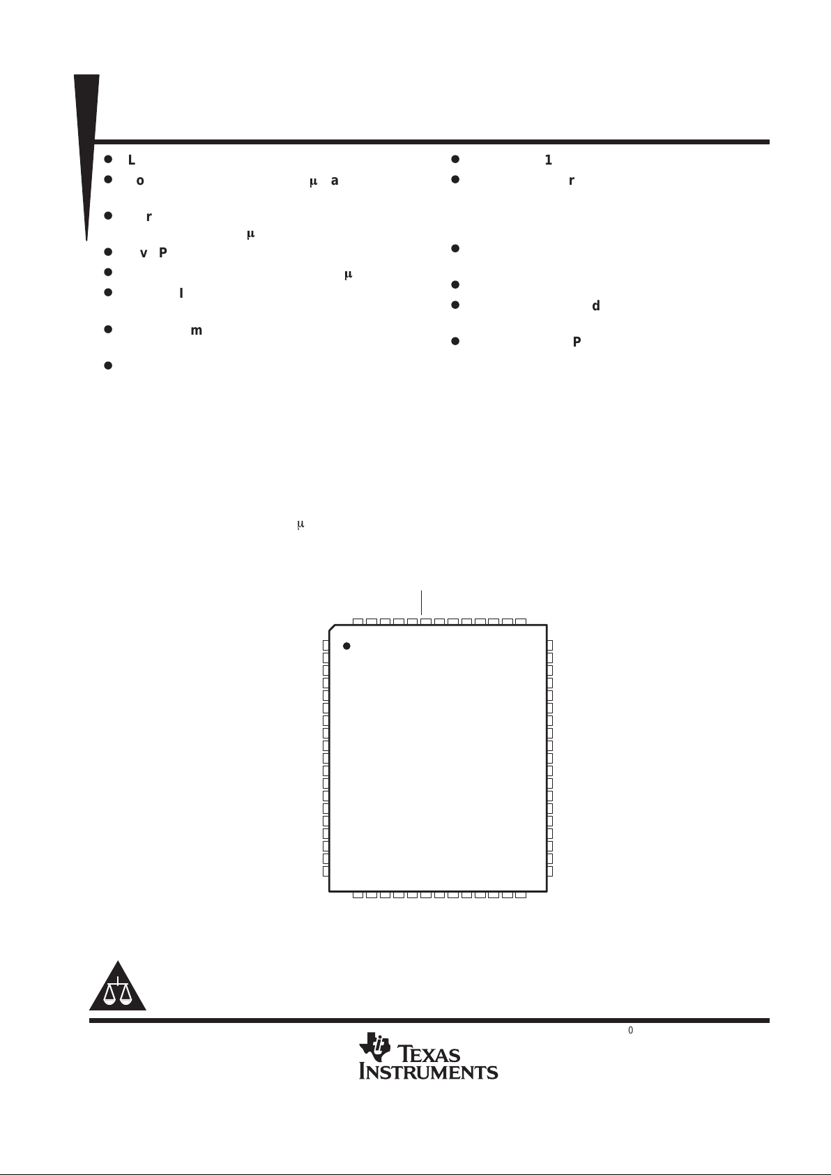
Avaliable in 64 Pin Quad Flatpack (QFP),
68 Pin Plastic J-Leaded Chip Carrier
(PLCC), 68 Pin J-Leaded Ceramic Chip
Carrier (JLCC) Package (EPROM Version)
description
The T exas Instruments MSP430 is an ultra-low power mixed-signal microcontroller family consisting of several
devices which feature different sets of modules targeted to various applications. The microcontroller is designed
to be battery operated for an extended application lifetime. With 16-bit RISC architecture, 16-bit integrated
registers on the CPU, and a constant generator, the MSP430 achieves maximum code ef ficiency . The digitallycontrolled oscillator, together with the frequency-locked-loop (FLL), provides a wakeup from a low-power mode
to active mode in less than 6 ms.
Copyright 2000, Texas Instruments Incorporated
PRODUCTION DATA information is current as of publication date.
Products conform to specifications per the terms of Texas Instruments
standard warranty. Production processing does not necessarily include
testing of all parameters.
Please be aware that an important notice concerning availability, standard warranty, and use in critical applications of
Texas Instruments semiconductor products and disclaimers thereto appears at the end of this data sheet.
1
2
3
4
5
6
7
8
9
10
11
12
13
14
15
16
17
18
19
51
50
49
48
47
46
45
44
43
42
41
40
39
38
37
36
35
34
33
202122 23 242526 272829303132
64 636261605958575655545352
PG Package
(TOP VIEW)
AV
CC
DV
CC
SV
CC
Rext
A2
A3
A4
A5
Xin
Xout/TCLK
CIN
TP0.0
TP0.1
TP0.2
TP0.3
TP0.4
TP0.5
P0.0
P0.1/RXD
COM0
S20/O20/CMPI
S19/O19
S18/O18
S17/O17
S16/O16
S15/O15
S14/O14
S13/O13
S12/O12
S1 1/O11
S10/O10
S9/O9
S8/O8
S7/O7
S6/O6
S5/O5
S4/O4
S3/O3
DV
SSAVSS
A1A0XBUF
RST/NMI
TCK
TMS
TDI/VPP
TDO/TDI
COM3
COM2
COM1
P0.2/TXD
P0.3
P0.4
P0.5
P0.6
P0.7
R33
R23
R13
R03
S0
S1
S2/O2
MSP430C32x, MSP430P325A
MIXED SIGNAL MICROCONTROLLER
SLAS219B – MARCH 1999 – REVISED MARCH 2000
2
POST OFFICE BOX 655303 • DALLAS, TEXAS 75265
description (continued)
Typical applications include sensor systems that capture analog signals, convert them to digital values, and then
process the data and display them or transmit them to a host system. The MSP430x32x offers an integrated
12+2 bit A/D converter with six multiplexed inputs.
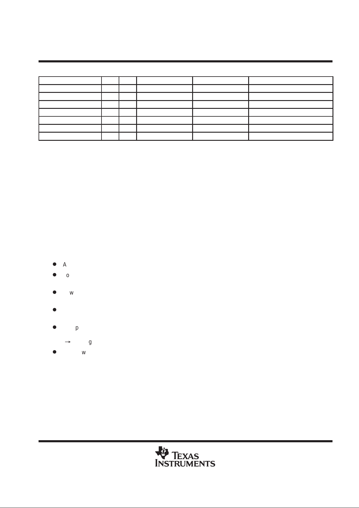
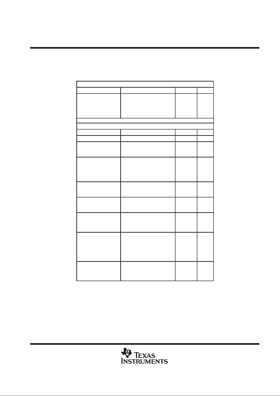
AVAILABLE OPTIONS
PACKAGED DEVICES
T
A
PLASTIC
64-PIN QFP
(PG)
PLASTIC
64-PIN QFP
(PM)
PLASTIC
68-PIN PLCC
(FN)
CERAMIC
68-PIN JLCC
(FZ)
°
°
MSP430C323IPG
MSP430C323IPM
MSP430C323IFN
–
40°C to 85°C
MSP430C325IPG
MSP430P325AIPG
MSP430C325IPM
MSP430P325AIPM
MSP430C325IFN
MSP430P325AIFN
—
°
25°C
— — —
PMS430E325AFZ
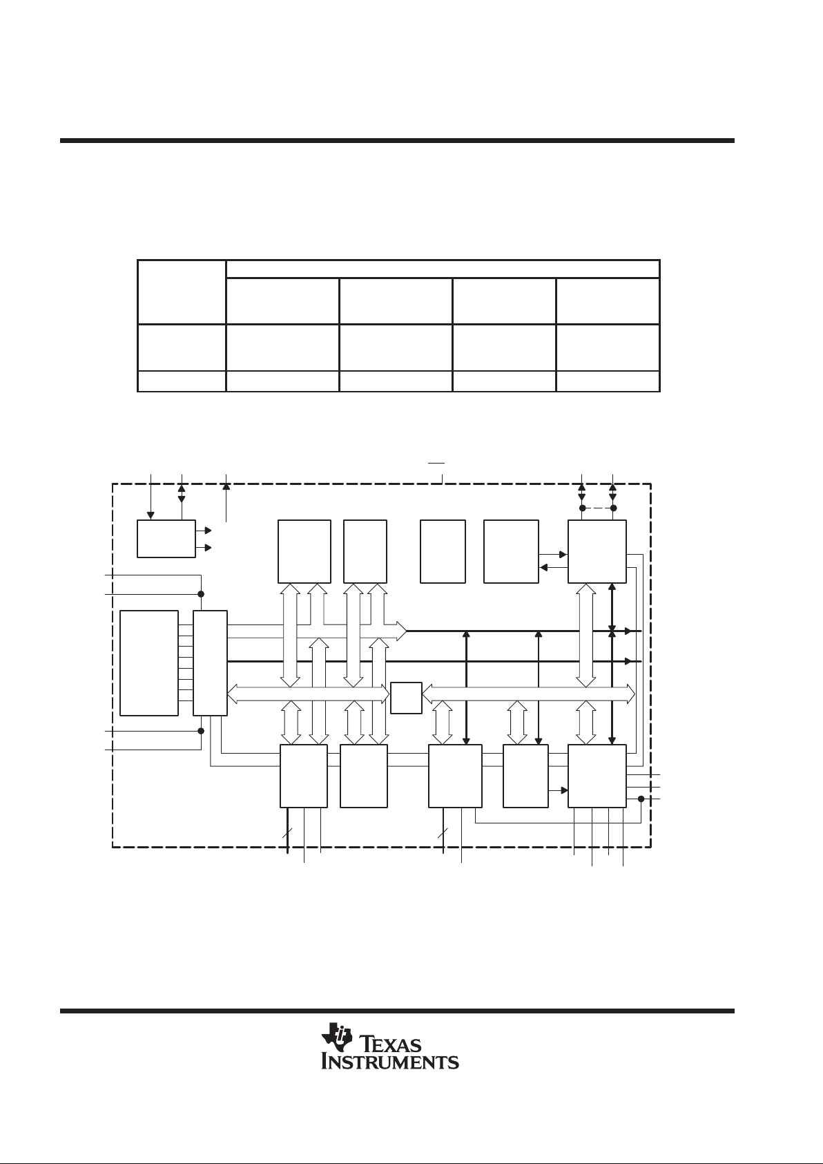
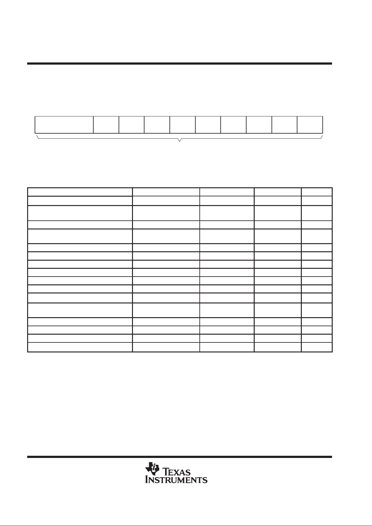
functional block diagram
Oscillator
FLL
System Clock
ACLK
MCLK
8/16 kB ROM
16 kB OTP
’C’: ROM
256/512 B
RAM
Power-on-
Reset
8 b Timer/
Counter
Serial Protocol
I/O Port
8 I/O’s, All With
Interr. Cap.
3 Int. Vectors
CPU
Incl. 16 Reg.
Test
JTAG
Bus
Conv
Timer/Port
Applications:
Timer, O/P
Basic
LCD
84 Segments
1, 2, 3, 4 MUX
Timer1
ADC
12 + 2 Bit
6 Channels
MAB, 16 Bit
MDB, 16 Bit
MAB, 4 Bit
MDB, 8 Bit
MCB
6
LCD
f
CMPI
TP0.0–5
CIN
XIN Xout/TCLK XBUF P0.0 P0.7
Com0–3
S0–19/O2–19
S20/O20CMPI
R33 R13
TDI/VPP
TDO/TDI
TMS
TCK
TXD
’P’: OTP
A/D Conv.
Support
RXD
Watchdog
timer
15/16 Bit
Current S.
6
A0–5
Rext
SVCC
RST/NMI
R23
R03
MSP430C32x, MSP430P325A
MIXED SIGNAL MICROCONTROLLER
SLAS219B – MARCH 1999 – REVISED MARCH 2000
3
POST OFFICE BOX 655303 • DALLAS, TEXAS 75265
Terminal Functions
TERMINAL
NAME NO.
I/O
DESCRIPTION
AV
CC
1 Positive analog supply voltage
AV
SS
63 Analog ground reference
A0 61 I Analog-to-digital converter input port 0 or digital input port 0
A1 62 I Analog-to-digital converter input port 1 or digital input port 1
A2–A5 5–8 I Analog-to-digital converter inputs ports 2–5 or digital inputs ports 2–5
CIN 11 I Input used as enable of counter TPCNT1 – Timer/Port
COM0–3 51–54 O Common outputs, used for LCD backplanes – LCD
DV
CC
2 Positive digital supply voltage
DV
SS
64 Digital ground reference
P0.0 18 I/O General-purpose digital I/O
P0.1/RXD 19 I/O General-purpose digital I/O, receive digital input port, 8-bit Timer/Counter
P0.2/TXD 20 I/O General-purpose digital I/O, transmit data output port, 8-bit Timer/Counter
P0.3–P0.7 21–25 I/O Five general-purpose digital I/Os, bit 3 to bit 7
Rext 4 I Programming resistor input of internal current source
RST/NMI 59 I Reset input or non-maskable interrupt input
R03 29 I Input of fourth positive analog LCD level (V4) – LCD
R13 28 I Input of third positive analog LCD level (V3) – LCD
R23 27 I Input of second positive analog LCD level (V2) – LCD
R33 26 O Output of first positive analog LCD level (V1) – LCD
SV
CC
3 Switched AVCC to analog-to-digital converter
S0 30 O Segment line S0 – LCD
S1 31 O Segment line S1 – LCD
S2–S5/O2–O5 32–35 O Segment lines S2 to S5 or digital output ports O2–O5, group 1 – LCD
S20/O20/CMPI 50 I/O Segment line S20 can be used as comparator input port CMPI – Timer/Port
S6–S9/O6–O9 36–39 O Segment lines S6 to S9 or digital output ports O6–O9, group 2 – LCD
S10–S13/O10–O13 40–43 O Segment lines S10 to S13 or digital output ports O10–O13, group 3 – LCD
S14–S17/O14–O17 44–47 O Segment lines S14 to S17 or digital output ports O14 to O17, group 4 – LCD
S18-S19/O18-O19 48, 49 O Segment lines S18 and S19 or digital output port O18 and O19, group 5 – LCD
TCK 58 I Test clock, clock input terminal for device programming and test
TDO/TDI 55 I/O Test data output, data output terminal or data input during programming
TDI/VPP 56 I Test data input, data input terminal or input of programming voltage
TMS 57 I Test mode select, input terminal for device programming and test
TP0.0 12 O General-purpose 3-state digital output port, bit 0 – Timer/Port
TP0.1 13 O General-purpose 3-state digital output port, bit 1 – Timer/Port
TP0.2 14 O General-purpose 3-state digital output port, bit 2 – Timer/Port
TP0.3 15 O General-purpose 3-state digital output port, bit 3 – Timer/Port
TP0.4 16 O General-purpose 3-state digital output port, bit 4 – Timer/Port
TP0.5 17 I/O General-purpose digital input/output port, bit 5 – Timer/Port
XBUF 60 O Clock signal output of system clock MCLK or crystal clock ACLK
Xin 9 I Input terminal of crystal oscillator
Xout/TCLK 10 I/O Output terminal of crystal oscillator or test clock input
MSP430C32x, MSP430P325A
MIXED SIGNAL MICROCONTROLLER
SLAS219B – MARCH 1999 – REVISED MARCH 2000
4
POST OFFICE BOX 655303 • DALLAS, TEXAS 75265
short-form description
processing unit
The processing unit is based on a consistent and orthogonally-designed CPU and instruction set. This design
structure results in a RISC-like architecture, highly transparent to the application development and is
distinguished due to ease of programming. All operations other than program-flow instructions are
consequently performed as register operations in conjunction with seven addressing modes for source and four
modes for destination operand.
CPU
Sixteen registers are located inside the CPU,
providing reduced instruction execution time. This
reduces a register-register operation execution
time to one cycle of the processor frequency.
Four of the registers are reserved for special
use as a program counter, a stack pointer , a status
register and a constant generator. The remaining
registers are available as general-purpose
registers.
Peripherals are connected to the CPU using a
data address and control bus and can be handled
easily with all instructions for memory
manipulation.
instruction set
The instruction set for this register-register architecture provides a powerful and easy-to-use assembler
language. The instruction set consists of 51 instructions with three formats and seven addressing modes.
T able 1 provides a summation and example of the three types of instruction formats; the addressing modes are
listed in Table 2.
Table 1. Instruction Word Formats
Dual operands, source-destination e.g. ADD R4, R5 R4 + R5 → R5
Single operands, destination only e.g. CALL R8 PC → (TOS), R8 → PC
Relative jump, un-/conditional e.g. JNE Jump-on equal bit = 0
Each instruction that operates on word and byte data is identified by the suffix B.
Examples: Instructions for word operation Instructions for byte operation
MOV EDE, TONI MOV.B EDE, TONI
ADD #235h, &MEM ADD.B #35h, &MEM
PUSH R5 PUSH.B R5
SWPB R5 —
Program Counter
General-Purpose Register
PC/R0
Stack Pointer
SP/R1
Status Register
SR/CG1/R2
Constant Generator
CG2/R3
R4
General-Purpose Register
R5
General-Purpose Register R14
General-Purpose Register
R15
MSP430C32x, MSP430P325A
MIXED SIGNAL MICROCONTROLLER
SLAS219B – MARCH 1999 – REVISED MARCH 2000
5
POST OFFICE BOX 655303 • DALLAS, TEXAS 75265
Table 2. Address Mode Descriptions
ADDRESS MODE s d SYNTAX EXAMPLE OPERATION
Register √ √ MOV Rs, Rd MOV R10, R11 R10 → R11
Indexed √ √ MOV X(Rn), Y(Rm) MOV 2(R5), 5(R6) M(2 + R5) → M(6 + R6)
Symbolic (PC relative) √ √ MOV EDE, TONI M(EDE) → M(TONI)
Absolute √ √ MOV &MEM, &TCDAT M(MEM) → M(TCDAT)
Indirect √ MOV @Rn, Y(Rm) MOV @R10, Tab(R6) M(R10) → M(Tab + R6)
Indirect autoincrement √ MOV @Rn+, RM MOV @R10+, R11 M(R10) → R11, R10 + 2 → R10
Immediate √ MOV #X, TONI MOV #45, TONI #45 → M(TONI)
NOTE: s = source d = destination
Computed branches (BR) and subroutine calls (CALL) instructions use the same addressing modes as the other
instructions. These addressing modes provide
indirect
addressing, ideally suited for computed branches and
calls. The full use of this programming capability permits a program structure different from conventional 8- and
16-bit controllers. For example, numerous routines can easily be designed to deal with pointers and stacks
instead of using flag type programs for flow control.
operation modes and interrupts
The MSP430 operating modes support various advanced requirements for ultra low power and ultra low energy
consumption. This is achieved by the intelligent management of the operations during the different module
operation modes and CPU states. The requirements are fully supported during interrupt event handling. An
interrupt event awakens the system from each of the various operating modes and returns with the RETI
instruction to the mode that was selected before the interrupt event. The clocks used are ACLK and MCLK.
ACLK is the crystal frequency and MCLK is a multiple of ACLK and is used as the system clock.
The software can configure five operating modes:
D
Active mode (AM). The CPU is enabled with different combinations of active peripheral modules.
D
Low power mode 0 (LPM0). The CPU is disabled, peripheral operation continues, ACLK and MCLK signals
are active, and loop control for MCLK is active.
D
Low power mode 1 (LPM1). The CPU is disabled, peripheral operation continues, ACLK and MCLK signals
are active, and loop control for MCLK is inactive.
D
Low power mode 2 (LPM2). The CPU is disabled, peripheral operation continues, ACLK signal is active,
and MCLK and loop control for MCLK are inactive.
D
Low power mode 3 (LPM3). The CPU is disabled, peripheral operation continues, ACLK signal is active,
MCLK and loop control for MCLK are inactive, and the dc generator for the digital controlled oscillator (DCO)
(³MCLK generator) is switched off.
D
Low power mode 4 (LPM4). The CPU is disabled, peripheral operation continues, ACLK signal is inactive
(crystal oscillator stopped), MCLK and loop control for MCLK are inactive, and the dc generator for the DCO
is switched off.
The special function registers (SFR) include module-enable bits that stop or enable the operation of the specific
peripheral module. All registers of the peripherals may be accessed if the operational function is stopped or
enabled. However, some peripheral current-saving functions are accessed through the state of local register
bits. An example is the enable/disable of the analog voltage generator in the LCD peripheral, which is turned
on or off using one register bit.
MSP430C32x, MSP430P325A
MIXED SIGNAL MICROCONTROLLER
SLAS219B – MARCH 1999 – REVISED MARCH 2000
6
POST OFFICE BOX 655303 • DALLAS, TEXAS 75265
operation modes and interrupts (continued)
The most general bits that influence current consumption and support fast turnon from low-power operating
modes are located in the status register (SR). Four of these bits control the CPU and the system clock generator:
SCG1, SCG0, OscOff, and CPUOff.
Reserved For Future
Enhancements
15 9 8 7 0
V SCG1 SCG0 OscOff CPUOff GIE N Z C
rw-0
interrupt vector addresses
The interrupt vectors and the power-up starting address are located in the ROM with an address range of
0FFFFh-0FFE0h. The vector contains the 16-bit address of the appropriate interrupt handler instruction
sequence.
INTERRUPT SOURCE INTERRUPT FLAG SYSTEM INTERRUPT WORD ADDRESS PRIORITY
Power-up, external reset, watchdog
WDTIFG
(see Note1)
Reset 0FFFEh 15, highest
NMI, oscillator fault
NMIIFG (see Notes 1 and 3)
OFIFG (see Notes 1 and 4)
Non-maskable,
(Non)-maskable
0FFFCh 14
Dedicated I/O P0.0 P0.0IFG maskable 0FFFAh 13
Dedicated I/O P0.1 or 8-bit Timer/Counter
RXD
P0.1IFG maskable 0FFF8h 12
0FFF6h 11
Watchdog Timer WDTIFG maskable 0FFF4h 10
0FFF2h 9
0FFF0h 8
0FFEEh 7
0FFECh 6
ADC ADCIFG maskable 0FFEAh 5
Timer/Port
RC1FG, RC2FG, EN1FG
(see Note 2)
maskable 0FFE8h 4
0FFE6h 3
0FFE4h 2
Basic Timer1 BTIFG maskable 0FFE2h 1
I/O port 0, P0.2–7
P0.27IFG (see Note 1)
maskable 0FFE0h 0, lowest
NOTE 1: Multiple source flags
NOTE 2: Timer/Port interrupt flags are located in the T/P registers
NOTE 3: Non-maskable: neither the individual nor the general interrupt enable bit will disable an interrupt event.
NOTE 4: (Non)-maskable: the individual interrupt enable bit can disable on interrupt event, but the general interrupt enable bit cannot.
MSP430C32x, MSP430P325A
MIXED SIGNAL MICROCONTROLLER
SLAS219B – MARCH 1999 – REVISED MARCH 2000
7
POST OFFICE BOX 655303 • DALLAS, TEXAS 75265
operation modes and interrupts (continued)
special function registers
Most interrupt and module enable bits are collected into the lowest address space. Special function register bits
that are not allocated to a functional purpose are not physically present in the device. Simple SW access is
provided with this arrangement.
interrupt enable 1 and 2
7654 0
P0IE.1 OFIE WDTIE
321
P0IE.0
rw-0 rw-0 rw-0 rw-0
Address
0h
WDTIE: Watchdog Timer enable signal
OFIE: Oscillator fault enable signal
P0IE.0: Dedicated I/O P0.0
P0IE.1: P0.1 or 8-bit Timer/Counter, RXD
7654 0
ADIE
rw-0
321
rw-0
Address
01h BTIE TPIE
rw-0
ADIE: A/D converter enable signal
TPIE: Timer/Port enable signal
BTIE: Basic Timer1 enable signal
interrupt flag register 1 and 2
7654 0
P0IFG.1 OFIFG WDTIFG
321
rw-0 rw-1 rw-0
Address
02h NMIIFG P0IFG.0
rw-0 rw-0
WDTIFG: Set on overflow or security key violation
or
Reset on VCC power on or reset condition at RST/NMI-pin
OFIFG: Flag set on oscillator fault
P0.0IFG: Dedicated I/O P0.0
P0.1IFG: P0.1 or 8-bit Timer/Counter, RXD
NMIIFG: Signal at RST
/NMI-pin
7654 0
rw
321
Address
03h BTIFG ADIFG
rw-0
BTIFG Basic Timer1 flag
ADFIG Analog-to-digital converter flag
MSP430C32x, MSP430P325A
MIXED SIGNAL MICROCONTROLLER
SLAS219B – MARCH 1999 – REVISED MARCH 2000
8
POST OFFICE BOX 655303 • DALLAS, TEXAS 75265
operation modes and interrupts (continued)
module enable register 1 and 2
7654 0321
Address
04h
7654 0321
Address
05h
Legend rw:
rw-0:
Bit can be read and written.
Bit can be read and written. It is reset by PUC.
SFR bit not present in device.
memory organization
Int. Vector
16 kB OTP
or
EPROM
512B RAM
16b Per.
8b Per.
SFR
FFFFh
FFE0h
FFDFh
C000h
03FFh
0200h
01FFh
0100h
00FFh
0010h
000Fh
0000h
MSP430P325A
PMS430E325A
Int. Vector
16 kB ROM
512B RAM
16b Per.
8b Per.
SFR
FFFFh
FFE0h
FFDFh
03FFh
0200h
01FFh
0100h
00FFh
0010h
000Fh
0000h
MSP430C325
C000h
Int. Vector
8 kB ROM
256B RAM
16b Per.
8b Per.
SFR
FFFFh
FFE0h
FFDFh
E000h
02FFh
0200h
01FFh
0100h
00FFh
0010h
000Fh
MSP430C323
0000h
MSP430C32x, MSP430P325A
MIXED SIGNAL MICROCONTROLLER
SLAS219B – MARCH 1999 – REVISED MARCH 2000
9
POST OFFICE BOX 655303 • DALLAS, TEXAS 75265
peripherals
Peripherals connect to the CPU through data, address, and control busses and can be handled easily with all
instructions for memory manipulation.
peripheral file map
PERIPHERALS WITH WORD ACCESS
Watchdog Watchdog Timer control WDTCTL 0120h
ADC Data register
Reserved
Control register
Input enable register
Input register
ADAT
ACTL
AEN
AIN
0118h
0116h
0114h
o112h
0110h
PERIPHERALS WITH BYTE ACCESS
EPROM EPROM control EPCTL 054h
Crystal buffer Crystal buffer control CBCTL 053h
System clock SCG frequency control
SCG frequency integrator
SCG frequency integrator
SCFQCTL
SCFI1
SCFI0
052h
051h
050h
Timer/Port T imer/Port enable
Timer/Port data
Timer/Port counter2
Timer/Port counter1
Timer/Port control
TPE
TPD
TPCNT2
TPCNT1
TPCTL
04Fh
04Eh
04Dh
04Ch
04Bh
8-Bit Timer/Counter 8-Bit Timer/Counter data
8-Bit Timer/Counter preload
8-Bit Timer/Counter control
TCDAT
TCPLD
TCCTL
044h
043h
042h
Basic Timer1 Basic Timer counter2
Basic Timer counter1
Basic Timer control
BTCNT2
BTCNT1
BTCTL
047h
046h
040h
LCD LCD memory 15
:
LCD memory 1
LCD control & mode
LCDM15
:
LCDM1
LCDCTL
03Fh
:
031h
030h
Port P0 Port P0 interrupt enable
Port P0 interrupt edge select
Port P0 interrupt flag
Port P0 direction
Port P0 output
Port P0 input
P0IE
P0IES
P0IFG
P0DIR
P0OUT
P0IN
015h
014h
013h
012h
011h
010h
Special function SFR interrupt flag2
SFR interrupt flag1
SFR interrupt enable2
SFR interrupt enable1
IFG2
IFG1
IE2
IE1
003h
002h
001h
000h
oscillator and system clock
Two clocks are used in the system, the system (master) clock (MCLK) and the auxiliary clock (ACLK). The MCLK
is a multiple of the ACLK. The ACLK runs with the crystal oscillator frequency. The special design of the oscillator
supports the feature of low current consumption and the use of a 32 768 Hz crystal. The crystal is connected
across two terminals without any other external components being required.
The oscillator starts after applying VCC, due to a reset of the control bit (OscOff) in the status register (SR). It
can be stopped by setting the OscOff bit to a 1. The enabled clock signals ACLK, ACLK/2, ACLK/4, or MCLK
are accessible for use by external devices at output terminal XBUF.
MSP430C32x, MSP430P325A
MIXED SIGNAL MICROCONTROLLER
SLAS219B – MARCH 1999 – REVISED MARCH 2000
10
POST OFFICE BOX 655303 • DALLAS, TEXAS 75265
oscillator and system clock (continued)
The controller system clock has to operate with different requirements according to the application and system
conditions. Requirements include:
D
High frequency in order to react quickly to system hardware requests or events
D
Low frequency in order to minimize current consumption, EMI, etc.
D
Stable frequency for timer applications e.g. real time clock (RTC)
D
Enable start-stop operation with a minimum of delay
These requirements cannot all be met with fast frequency high-Q crystals or with RC-type low-Q oscillators. The
compromise selected for the MSP430 uses a low-crystal frequency which is multiplied to achieve the desired
nominal operating range:
f
(system)
= (N+1) × f
(
crystal)
The crystal frequency multiplication is acheived with a frequency locked loop (FLL) technique. The factor N is
set to 31 after a power-up clear condition. The FLL technique, in combination with a digital controlled oscillator
(DCO) provides immediate start-up capability together with long term crystal stability . The frequency variation
of the DCO with the FLL inactive is typically 330 ppm which means that with a cycle time of 1 µs the maximum
possible variation is 0.33 ns. For more precise timing, the FLL can be used which forces longer cycle times if
the previous cycle time was shorter than the selected one. This switching of cycle times makes it possible to
meet the chosen system frequency over a long period of time.
The start-up operation of the system clock depends on the previous machine state. During a power up clear
(PUC), the DCO is reset to its lowest possible frequency. The control logic starts operation immediately after
recognition of PUC. Connect operation of the FLL control logic requires the presence of a stable crystal
oscillator.
digital I/O
One 8-bit I/O port (Port0) is implemented. Six control registers give maximum flexibility of digital input/output
to the application:
D
All individual I/O bits are programmable independently.
D
Any combination of input, output, and interrupt conditions is possible.
D
Interrupt processing of external events is fully implemented for all eight bits of port P0.
D
Provides read/write access to all registers with all instructions.
The six registers are:
D
Input register Contains information at the pins
D
Output register Contains output information
D
Direction register Controls direction
D
Interrupt flags Indicates if interrupt(s) are pending
D
Interrupt edge select Contains input signal change necessary for interrupt
D
Interrupt enable Contains interrupt enable pins
All six registers contain eight bits except for the interrupt flag register and the interrupt enable register. The two
LSBs of the interrupt flag and interrupt enable registers are located in the special functions register (SFR). Three
interrupt vectors are implemented, one for Port0.0, one for Port0.1, and one commonly used for any interrupt
event on Port0.2 to Port0.7. The Port0.1 and Port0.2 pin function is shared with the 8-bit Timer/Counter.

MSP430C32x, MSP430P325A
MIXED SIGNAL MICROCONTROLLER
SLAS219B – MARCH 1999 – REVISED MARCH 2000
11
POST OFFICE BOX 655303 • DALLAS, TEXAS 75265
LCD drive
Liquid crystal displays (LCDs) for static, 2-, 3- and 4-MUX operations can be driven directly . The controller LCD
logic operation is defined by software using memory-bit manipulation. LCD memory is part of the LCD module,
not part of data memory . Eight mode and control bits define the operation and current consumption of the LCD
drive. The information for the individual digits can be easily obtained using table programming techniques
combined with the correct addressing mode. The segment information is stored in LCD memory using
instructions for memory manipulation.
The drive capability is mainly defined by the external resistor divider that supports the analog levels for 2-, 3and 4-MUX operation. Groups of the LCD segment lines can be selected for digital output signals. The
MSP430x32x configuration has four common signal lines and 21 segment lines.
A/D converter
The analog-to-digital converter (ADC) is a cascaded converter type that converts analog signals from VCC to
GND. It is a 12+2 bit converter with a software or automatically-controlled range select. Five inputs can be
selected for analog or digital function. A ratiometric current source can be used on four of the analog pins. The
current is adjusted by an external resistor and is enabled/disabled by bits located in the control registers. The
conversion is started by setting the start-of-conversion bit (SOC) in the control register and the
end-of-conversions sets the interrupt flag. The analog input signal is sampled starting with SOC during the next
twelve MCLK clock pulses. The power-down bit in the control register controls the operating mode of the ADC
peripheral. The current consumption and operation is stopped when it is set. The system reset PUC sets the
power-down bit.
Basic Timer1
The Basic Timer1 (BT1) divides the frequency of MCLK or ACLK, as selected with the SSEL bit, to provide low
frequency control signals. This is done within the system by one central divider, the Basic Timer1, to support
low current applications. The BTCTL control register contains the flags which controls or selects the different
operational functions. When the supply voltage is applied or when a reset of the device (RST
/NMI pin), a
watchdog overflow, or a watchdog security key violation occurs, all bits in the register hold undefined or
unchanged status. The user software usually configures the operational conditions on the BT1 during
initialization.
The Basic Timer1 has two 8-bit timers which can be cascaded to a 16-bit timer. Both timers can be read and
written by software. Two bits in the SFR address range handle the system control interaction according to the
function implemented in the Basic Timer1. These two bits are the Basic T imer1 interrupt flag (BTIFG) and the
Basic Timer1 interrupt enable (BTIE) bit.
Watchdog Timer
The primary function of the Watchdog Timer (WDT) module is to perform a controlled system restart after a
software upset has occurred. If the selected time interval expires, a system reset is generated. If this watchdog
function is not needed in an application, the module can work as an interval timer, which generates an interrupt
after the selected time interval.
The Watchdog T imer counter (WDTCNT) is a 15/16-bit up-counter which is not directly accessible by software.
The WDTCNT is controlled using the Watchdog T imer control register (WDTCTL), which is an 8-bit read/write
register. W riting to WDTCTL, in both operating modes (watchdog or timer) is only possible by using the correct
password in the high-byte. The low-byte stores data written to the WDTCTL. The high-byte password is 05Ah.
If any value other than 05Ah is written to the high-byte of the WDTCTL, a system reset PUC is generated.
When
the password is read it’s value is 069h
. This minimizes accidental write operations to the WDTCTL register. In
addition to the Watchdog Timer control bits, two bits included in the WDTCTL configure the NMI pin.

MSP430C32x, MSP430P325A
MIXED SIGNAL MICROCONTROLLER
SLAS219B – MARCH 1999 – REVISED MARCH 2000
12
POST OFFICE BOX 655303 • DALLAS, TEXAS 75265
8-bit Timer/Counter
The 8-bit interval timer supports three major functions for the application:
D
Serial communication or data exchange
D
Pulse counting or pulse accumulation
D
Timer
The 8-bit Timer/Counter peripheral includes the following major blocks: an 8-bit Up-Counter with preload
register, an 8-bit control register, an Input clock selector, an edge detection (e.g. Start bit detection for
asynchronous protocols), and an input and output data latch, triggered by the carry-out-signal from the 8-bit
counter.
The 8-bit counter counts up with an input clock which is selected by two control bits from the control register.
The four possible clock sources are MCLK, ACLK, the external signal from terminal P0.1, and the signal from
the logical AND of MCLK and terminal P0.1.
Two counter inputs (load, enable) control the counter operation. The load input controls load operations. A
write-access to the counter results in loading the content of the preload register into the counter. The software
writes or reads the preload register with all instructions. The preload register acts as a buffer and can be written
immediately after the load of the counter is completed. The enable input enables the count operation. When
the enable signal is set HIGH, the counter will count-up each time a positive clock edge is applied to the clock
input of the counter.
Serial protocols, like UART protocol, need start-bit edge-detection to determine, at the receiver, the start of a
data transmission. When this function is activated, the counter starts counting after the start-bit condition is
detected. The first signal level is sampled into the RXD input data-latch after completing the first timing interval,
which is programmed into the counter. T wo latches are used for input and output data (RXD_FF and TXD_FF)
are clocked by the counter after the programmed timing interval has elapsed.
UART
The serial communication is realized by using software and the 8-bit Timer/Counter hardware. The hardware
supports the output of the serial data stream, bit-by-bit, with the timing determined by the counter. The
software/hardware interface connects the mixed signal controller to external devices, systems, or networks.
Timer/Port
The Timer/Port module has two 8-bit counters, an input that triggers one counter , and six 3-state digital outputs.
Both counters have an independent clock-selector for selecting an external signal or one of the internal clocks
(ACLK or MCLK). One of the counters has an extended control capability to halt, count continuously, or gate
the counter by selecting one of two external signals. This gate signal sets the interrupt flag, if an external signal
is selected, and the gate stops the counter.
Both timers can be read from and written to by software. The two 8-bit counters can be cascaded to a 16-bit
counter. A common interrupt vector is implemented. The interrupt flag can be set from three events in the 8-bit
counter mode (gate signal, overflow from the counters) or from two events in the 16-bit counter mode (gate
signal, overflow from the MSB of the cascaded counter).

MSP430C32x, MSP430P325A
MIXED SIGNAL MICROCONTROLLER
SLAS219B – MARCH 1999 – REVISED MARCH 2000
13
POST OFFICE BOX 655303 • DALLAS, TEXAS 75265
absolute maximum ratings
†
Voltage applied at VCC to VSS (see Note 5) –0.3 V to 6 V. . . . . . . . . . . . . . . . . . . . . . . . . . . . . . . . . . . . . . . . . . .
Voltage applied to any pin (referenced to VSS) –0.3 V to VCC + 0.3 V. . . . . . . . . . . . . . . . . . . . . . . . . . . . . . . . . .
Diode current at any device terminal ± 2 mA. . . . . . . . . . . . . . . . . . . . . . . . . . . . . . . . . . . . . . . . . . . . . . . . . . . . . . . .
Storage temperature,T
stg
(unprogrammed device) –55°C to 150°C. . . . . . . . . . . . . . . . . . . . . . . . . . . . . . . . . . .
T
stg
(programmed device) –40°C to 85°C. . . . . . . . . . . . . . . . . . . . . . . . . . . . . . . . . . . . . .
†
Stresses beyond those listed under “absolute maximum ratings” may cause permanent damage to the device. These are stress ratings only, and
functional operation of the device at these or any other conditions beyond those indicated under “recommended operating conditions” is not
implied. Exposure to absolute-maximum-rated conditions for extended periods may affect device reliability.
NOTE 5: All voltage values relative to VSS.
recommended operating conditions
MIN NOM MAX UNIT
Supply voltage, VCC (MSP430C32x) 2.5 5.5 V
Supply voltage, VCC (MSP430P/E325A) 2.5 5.5 V
Supply voltage, during programming OTP/EPROM
(AVCC = DVCC = VCC)
MSP430P325A, PMS430E325A 4.5 5 5.5 V
Supply voltage, V
SS
0 V
p
p
MSP430C32x, MSP430P325A –40 85
°
Operating free-air temperature range, T
A
PMS430E325A 25
°C
XTAL frequency, f
(XTAL)
32 768 Hz
VCC = 3 V DC 2.2
Processor frequency (signal MCLK), f
(system)
VCC = 5 V DC 3.3
MH
z
Low-level input voltage, VIL (excluding Xin, Xout) V
SS
VSS+0.8
High-level input voltage, VIH (excluding Xin, Xout)
0.7 V
CC
V
CC
V
Low-level input voltage, V
IL(Xin, Xout)
V
CC
= 3
V/5 V
V
SS
0.2×V
CC
High-level input voltage, V
IH(Xin, Xout)
0.8×V
CC
V
CC
V
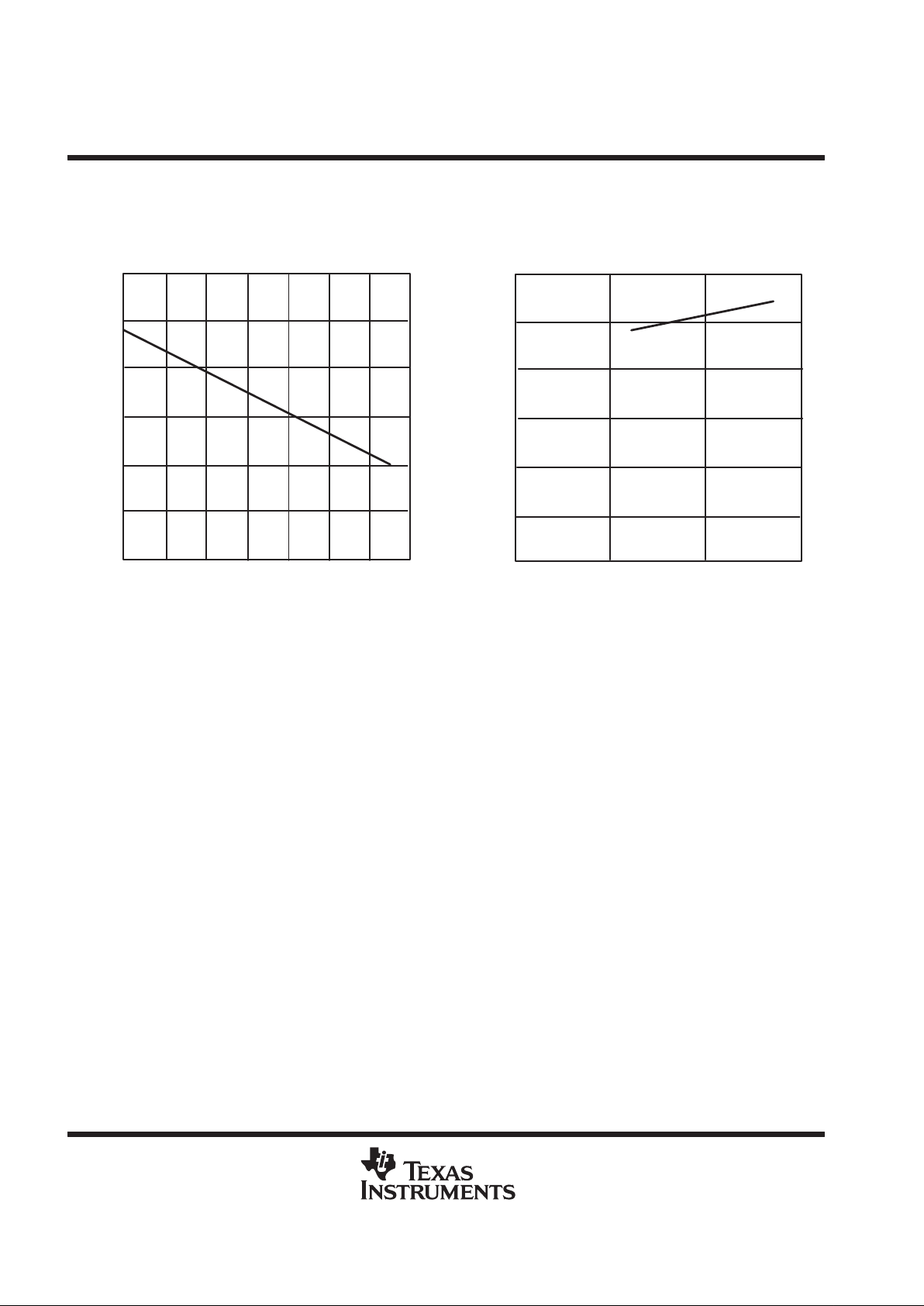
2.5 3 5 5.5
f(MHz)
3.3
2.2
1.1
VCC (V)
VCC – Supply Voltage – V
f
(system)
– Maximum Processor
Frequency – MHz
Minimum
NOTE: Minimum processor frequency is defined by system clock.
Figure 1. Processor Frequency vs Supply Voltage

MSP430C32x, MSP430P325A
MIXED SIGNAL MICROCONTROLLER
SLAS219B – MARCH 1999 – REVISED MARCH 2000
14
POST OFFICE BOX 655303 • DALLAS, TEXAS 75265
electrical characteristics over recommended operating free-air temperature range (unless
otherwise noted)
supply current into AVCC+DV
CC
excluding external current, f
system
= 1 MHz
PARAMETER TEST CONDITIONS MIN TYP MAX UNIT
TA = –40°C to 85°C, VCC = 3 V 400 500
Active mode, A/D conversion in
C32
x
TA = –40°C to 85°C, VCC = 5 V 800 900
I
(AM)
,
power-down
TA = –40°C to 85°C, VCC = 3 V 500 550
µ
A
P325A
TA = –40°C to 85°C, VCC = 5 V 950 1050
TA = –40°C to 85°C, VCC = 3 V 50 70
p
C32
x
TA = –40°C to 85°C, VCC = 5 V 100 130
I
(CPUOff)
Low power mode, (LPM0, LPM1)
TA = –40°C to 85°C, VCC = 3 V 50 70
µ
A
P325A
TA = –40°C to 85°C, VCC = 5 V 100 130
p
TA = –40°C to 85°C, VCC = 3 V 6 12
I
(LPM2)
Low power mode, (LPM2)
TA = –40°C to 85°C, VCC = 5 V 15 25
µ
A
TA = –40°C 1.5 2.4
TA = 25°C
VCC = 3 V
1.3 2
p
TA = 85°C 1.6 2.8
I
(LPM3)
Low power mode, (LPM3)
TA = –40°C 5.2 7
µ
A
TA = 25°C
VCC = 5 V
4.2 6.5
TA = 85°C 4 7
TA = –40°C 0.1 0.8
I
(LPM4)
Low power mode, (LPM4)
TA = 25°C
VCC = 3 V/5 V
0.1 0.8
µA
()
TA = 85°C 0.4 1.3
NOTE: All inputs are tied to 0 V or VCC. Outputs do not source or sink any current. The current consumption in LPM2, LPM3 and LPM4 are
measured with active Basic Timer1 (ACLK selected) and LCD Module (f
(LCD)
=1024 Hz, 4 MUX).
current consumption of active mode versus system frequency
I
AM
= I
AM[1 MHz]
× f
system
[MHz]
current consumption of active mode versus supply voltage
IAM = I
AM[3 V]
+ 200 µA/V × (VCC–3 V)
Schmitt-trigger inputs Port 0, P0.x Timer/Port, CIN, TP 0.5
PARAMETER TEST CONDITIONS MIN TYP MAX UNIT
p
VCC = 3 V 1.2 2.1
V
IT+
Positive-going input threshold voltage
VCC = 5 V 2.3 3.4
p
VCC = 3 V 0.5 1.35
V
IT–
Negative-going input threshold voltage
VCC = 5 V 1.4 2.3
V
VCC = 3 V 0.3 1
V
hys
Hysteresis (V
IT+
–
V
IT–
)
VCC = 5 V 0.6 1.4

MSP430C32x, MSP430P325A
MIXED SIGNAL MICROCONTROLLER
SLAS219B – MARCH 1999 – REVISED MARCH 2000
15
POST OFFICE BOX 655303 • DALLAS, TEXAS 75265
electrical characteristics over recommended operating free-air temperature range (unless
otherwise noted) (continued)
outputs – Port 0: P0.x; Timer/Port: TP0.0...5; LCD: Sxx/Oxx; XBUF, (see Note 6)
PARAMETER TEST CONDITIONS MIN TYP MAX UNIT
IOH = –1.2 mA, VCC = 3 V, See Note 6 VCC–0.4 V
CC
p
IOH = –3.5 mA, VCC = 3 V, See Note 7 VCC–1 V
CC
VOHHigh-level output current
IOH = –1.5 mA, VCC = 5 V, See Note 6 VCC–0.4 V
CC
V
IOH = –4.5 mA, VCC = 5 V, See Note 7 VCC–1 V
CC
IOL = 1.2 mA, VCC = 3 V, See Note 6 V
SS
VSS+0.4
p
IOL = 3.5 mA, VCC = 3 V, See Note 7 V
SS
VSS+1
VOLLow-level out ut voltage
IOL = 1.5 mA, VCC = 5 V, See Note 6 V
SS
VSS+0.4
V
IOL = 4.5 mA, VCC = 5 V, See Note 7 V
SS
VSS+1
NOTES: 6. The maximum total current, IOHmax and IOLmax, for all outputs combined, should not exceed ±9.6 mA to satisfy the maximum
voltage drop specified.
7. The maximum total current, IOHmax and IOLmax, for all outputs combined, should not exceed ±20 mA to satisfy the maximum voltage
drop specified.
leakage current (see Note 8)
PARAMETER TEST CONDITIONS MIN TYP MAX UNIT
I
lkg(TP)
Leakage current, Timer/Port
Timer/Port: V
(TP0.x,CIN
)
(see Note 9)
±50 nA
I
lkg(P0x)
Leakage current, port 0
Port 0: V
(P0.x)
(see Note 10)
±50 nA
I
lkg(S20)
Leakage current, S20 V
(S20)
= VSS to V
CC
VCC = 3 V/5 V
±50 nA
I
lkg(Ax)
Leakage current, ADC
ADC: Ax, x= 0 to 5
(see Note 11)
±30 nA
I
lkg(RST
/NMI)
Leakage current, RST/NMI ±50 nA
NOTES: 8. The leakage current is measured with VSS or VCC applied to the corresponding pin(s), unless otherwise noted.
9. All Timer/Port pins TP0.0 to TP0.5 are Hi-Z. Pins CIN and TP.0 to TP0.5 are connected together during leakage current
measurement. In the leakage measurement the input CIN is included. The input voltage is VSS or VCC.
10. The port pin must be selected for input and there must be no optional pullup or pulldown resistor.
11. The input voltage is V
(IN)
= VSS to VCC , the current source is off, AEN.x bit is normally reset to stop throughput current flowing from
VCC to VSS terminal.
optional resistors (see Note 12)
PARAMETER TEST CONDITIONS MIN TYP MAX UNIT
R
(opt1)
VCC = 3 V/5 V 1.2 2.4 4.8 kΩ
R
(opt2)
VCC = 3 V/5 V 1.8 3.6 7.2 kΩ
R
(opt3)
VCC = 3 V/5 V 3.6 7.3 14.6 kΩ
R
(opt4)
VCC = 3 V/5 V 5.5 11 22 kΩ
R
(opt5)
Resistors, individually programmable with ROM code, all port pins,
VCC = 3 V/5 V 11 22 44 kΩ
R
(opt6)
yg
values applicable for pulldown and pullup
VCC = 3 V/5 V 22 44 88 kΩ
R
(opt7)
VCC = 3 V/5 V 33 66 132 kΩ
R
(opt8)
VCC = 3 V/5 V 55 110 220 kΩ
R
(opt9)
VCC = 3 V/5 V 77 154 310 kΩ
R
(opt10)
VCC = 3 V/5 V 100 200 400 kΩ
NOTE 12: Optional resistors R
(optx)
for pulldown or pullup are not programmed in standard OTP/EPROM devices P/E 325A.

MSP430C32x, MSP430P325A
MIXED SIGNAL MICROCONTROLLER
SLAS219B – MARCH 1999 – REVISED MARCH 2000
16
POST OFFICE BOX 655303 • DALLAS, TEXAS 75265
electrical characteristics over recommended operating free-air temperature range (unless
otherwise noted) (continued)
input frequency – Port 0: P0.1; Timer/Port: CIN, TP0.5
PARAMETER TEST CONDITIONS MIN TYP MAX UNIT
f
(IN)
Input frequency DC f
(system)
MHz
P0.x, CIN, TP.5
3 V 300 ns
t
(H)
or t
(L)
High level or low level time
5 V 125 ns
output frequency
PARAMETER TEST CONDITIONS MIN TYP MAX UNIT
f
XBUF
XBUF, CL = 20 pF f
(system)
MHz
f
MCLK
= 1.1 MHz 40% 60%
t
Xdc
Duty cycle of O/P frequency
XBUF
,
C
L
= 20 pF,
=
f
XBUF
= f
ACLK
35% 65%
V
CC
= 3
V/5 V
f
XBUF
= f
ACLK/n
50%
external interrupt timing
PARAMETER TEST CONDITIONS MIN TYP MAX UNIT
t
(int)
Port P0: External trigger signal for the
interrupt flag (see Notes 13 and 14)
1.5 cycle
NOTES: 13. The external signal sets the interrupt flag every time t
(int)
is met. It may be set even with trigger signals shorter than t
(int)
. The
conditions to set the flag must be met independently of this timing constraint. Input frequency (t
(int)
) is defined in MCLK cycles.
14. The external signal needs additionally a timing resulting from the maximum input frequency constraint.
RAM
PARAMETER TEST CONDITIONS MIN TYP MAX UNIT
V
RAMh
CPU halted (see Note 15) 1.8 V
NOTE 15: This parameter defines the minimum supply voltage when the data in the program memory RAM remains unchanged. No program
execution should take place during this supply voltage condition.

MSP430C32x, MSP430P325A
MIXED SIGNAL MICROCONTROLLER
SLAS219B – MARCH 1999 – REVISED MARCH 2000
17
POST OFFICE BOX 655303 • DALLAS, TEXAS 75265
electrical characteristics over recommended operating free-air temperature range (unless
otherwise noted) (continued)
DCO
PARAMETER TEST CONDITIONS MIN TYP MAX UNIT
f
(NOM)
DCO N
DCO
= 1A0h, FN_4=FN_3=FN_2=0 VCC = 3 V/5 V 1 MHz
VCC = 3 V 0.15 0.6
f
DCO3
N
DCO
= 00
0110 0000
, FN_4=FN_3=FN_2=
0
VCC = 5 V 0.18 0.62
f
(NOM)
VCC = 3 V 1.25 4.7
MH
z
f
DCO26
N
DCO
= 11
0100 0000 FN_4=FN_3=FN_2=0
VCC = 5 V 1.45 5.5
VCC = 3 V 0.36 1.05
f
DCO3
N
DCO
= 00
0110 0000
, FN_4=FN_3=0, FN_2=
1
VCC = 5 V 0.39 1.2
2xf
(NOM)
VCC = 3 V 2.5 8.1
MHz
f
DC26
N
DCO
= 11
0100 0000
, FN_4=FN_3=0, FN_2=
1
VCC = 5 V 3 9.9
VCC = 3 V 0.5 1.5
f
DCO3
N
DCO
=
00 0110 0000
, FN_4=0, FN_3= 1, FN_2=
X
VCC = 5 V 0.6 1.8
3xf
(NOM)
VCC = 3 V 3.7 11
MHz
f
DCO26
N
DCO
=
11 0100 0000
, FN_4= 0, FN_3=1, FN_2=
X
VCC = 5 V 4.5 13.8
VCC = 3 V 0.7 1.85
f
DCO3
N
DCO
= 00
0110 0000 FN_4 =1, FN_3=FN_2=X
VCC = 5 V 0.8 2.4
4xf
(NOM)
VCC = 3 V 4.8 13.3
MHz
f
DCO26
N
DCO
= 11
0100 0000
, FN_4=1, FN_3=FN_2=
X
VCC = 5 V 6 17.7
N
DCO
f
MCLK
= f
NOM
, FN_4=FN_3=FN_2=0 VCC = 3 V/5 V A0h 1A0h 340h
S f
NDCO+1
= S × f
NDCO
VCC = 3 V/5 V 1.07 1.13
Legend
Tolerance at Tap 26
DCO Frequency
Adjusted by Bits
2∧9–2∧5 in SCFI1
Tolerance at Tap 3
4xf
NOM
3xf
NOM
2xf
NOM
f
NOM
f
(DCO26)
f
(DCO3)
f
(DCO26)
f
(DCO3)
f
(DCO26)
f
(DCO3)
f
(DCO26)
f
(DCO3)
FN_2 = 0
FN_3 = 0
FN_4 = 0
FN_2 = 1
FN_3 = 0
FN_4 = 0
FN_2 = X
FN_3 = 1
FN_4 = 0
FN_2 = X
FN_3 = X
FN_4 = 1
Figure 2

MSP430C32x, MSP430P325A
MIXED SIGNAL MICROCONTROLLER
SLAS219B – MARCH 1999 – REVISED MARCH 2000
18
POST OFFICE BOX 655303 • DALLAS, TEXAS 75265
electrical characteristics over recommended operating free-air temperature range (unless
otherwise noted) (continued)
crystal oscillator
PARAMETER TEST CONDITIONS MIN NOM MAX UNIT
C
(Xin)
Integrated capacitance at input VCC = 3 V/5 V 12 pF
C
(Xout)
Integrated capacitance at output VCC = 3 V/5 V 12 pF
PUC/POR
PARAMETER TEST CONDITIONS MIN NOM MAX UNIT
t
(POR_delay)
150 250 µs
TA = –40°C 1.5 2.4 V
V
(POR)
POR
TA = 25°C
1.2 2.1 V
()
TA = 85°C
V
CC
= 3
V/5 V
0.9 1.8 V
V
(min)
0 0.4 V
t
(reset)
PUC/POR Reset is accepted internally 2 µs
VCC
POR
V
t
V
(POR)
V
(min)
POR
No POR
Figure 3. Power-On Reset (POR) vs Supply Voltage
1.8
2.1
2.4
0.9
1.2
1.5
0
0.5
1
1.5
2
2.5
3
–40 –20 0 20 40 60 80
Temperature [°C]
25°C
V POR [V]
MAX
MIN
Figure 4. V
(POR)
vs Temperature
MSP430C32x, MSP430P325A
MIXED SIGNAL MICROCONTROLLER
SLAS219B – MARCH 1999 – REVISED MARCH 2000
19
POST OFFICE BOX 655303 • DALLAS, TEXAS 75265
electrical characteristics over recommended operating free-air temperature range (unless
otherwise noted) (continued)
LCD
PARAMETER TEST CONDITIONS MIN TYP MAX UNIT
V
O(HLCD)
Output 1 (HLCD) I
(HLCD)
<= 10 nA
VCC–0.125 V
CC
V
O(LLCD)
Output 0 (LLCD) I
(LLCD)
<= 10 nA
V
CC
= 3
V/5 V
V
SS
VSS+0.125
V
I
I(R03)
R03 = V
SS,
No load at all seg and com pins
I
I(R13)
Input leakage
R13 = VCC/ 3,
No load at all seg and com pins
VCC = 3 V/5 V ±20 nA
I
I(R23)
R23 = 2 VCC/ 3,
No load at all seg and com pins
r
o(Rx3 to Sxx)
Resistance I
(SXX)
= –3 µA, VCC = 3 V/5 V 50 kΩ
comparator (Timer/Port)
PARAMETER TEST CONDITIONS MIN TYP MAX UNIT
p
VCC = 3 V 250 350
I
(com)
Comparator (Timer/Port)
CPON
=
1
VCC = 5 V 450 600
µ
A
V
ref(com)
Internal reference voltage at (–) terminal CPON = 1 VCC = 3 V/5 V 0.23×V
CC
0.25×V
CC
0.26×V
CC
V
p
p
VCC = 3 V 5 37
V
h
ys(com
)
In ut hysteresis (com arator)
CPON
=
1
VCC =5 V 10 42
mV
wake-up LPM3
PARAMETER TEST CONDITIONS MIN TYP MAX UNIT
VCC = 3 V
f
= 1 MHz
VCC = 5 V
6
t
(LPM3)
Delay time
VCC = 3 V
µs
()
f
= 2 MHz
VCC = 5 V
6
f = 3 MHz VCC = 5 V 6
ADC supply current (f
(ADCLK)
= 1 MHz)
PARAMETER TEST CONDITIONS MIN NOM MAX UNIT
I
(ADC)
SVCC on, current source off, VCC = 3 V 200 400 µA
I
(ADC)
ADC current
SVCC on, current source off, VCC = 5 V 300 740 µA
SVCC (switched AVCC)
PARAMETER TEST CONDITIONS MIN NOM MAX UNIT
V
(SVCC)
SVCC on, I
(SVCC)
= –8 mA, VCC = 2.5 V VCC–0.2 V V
CC
V
I
(SVCC)
SVCC off, SVCC = 0 V, VCC = 5 V ±0.1 µA
Z
(SVCC)
Input impedance SVCC off, VCC = 3 V/5 V 40 100 kΩ

MSP430C32x, MSP430P325A
MIXED SIGNAL MICROCONTROLLER
SLAS219B – MARCH 1999 – REVISED MARCH 2000
20
POST OFFICE BOX 655303 • DALLAS, TEXAS 75265
electrical characteristics over recommended operating free-air temperature range (unless
otherwise noted) (continued)
current source (ADC)
PARAMETER TEST CONDITIONS MIN TYP MAX UNIT
V
(Rext)
Voltage, (Rext)
V
(Rext)
= V
(SVCC)
– V
(RI),
I
(RI)
= 6 mA,
VCC = 3 V/5 V, 0.246 ×
V
(SVCC)
0.249 ×
V
(SVCC)
0.252 ×
V
(SVCC)
V
R
(ext)
External resistor VCC = 3 V/5 V 95 1600 Ω
VA0..A3 = 0 .. 0.4 × V
(SVCC)
, IS =
V
(Rext)/R(ext)
= 1 mA
VCC = 3 V,
–1 1 µA
p
VA0..A3 = 0 .. 0.4 × V
(SVCC)
,
IS = V
(Rext)/R(ext)
= 6 mA
VCC = 3 V,
–3.2 3.2 µA
∆ISLoad compliance
VA0..A3 = 0 .. 0.5 × V
(SVCC)
IS = V
(Rext)/R(ext)
= 1 mA
VCC = 5 V,
–1.5 1.5 µA
VA0..A3 = 0 .. 0.5 × V
(SVCC)
IS = V
(Rext)/R(ext)
= 6 mA
VCC = 5 V,
–3.2 3.2 µA
A/D converter (f
(ADCLK)
= 1 MHz)
PARAMETER TEST CONDITIONS MIN TYP MAX UNIT
Resolution 12 + 2 bits
12-bit conversion
0.1 1.5
f
(con)
Conversion frequency
f
(con)
=
f
(ADCLK)
12+2-bit conversion
V
CC
=
3 V/5 V
0.14 1.5
MHz
12-bit conversion
96
cycles of
f
(concyc)
Conversion cycles
f
(ADCLK)
=
f
(MCLK)
/N
12+2-bit conversion
V
CC
=
3 V/5 V
132
y
ADCLK
LSB Voltage VCC = 3 V/5 V 0.000061×V
SVCC
V
INL
1
0 ≤ DDV ≤ 127 VCC = 3 V/5 V
–2 2
LSB
INL
2
Integral nonlinearity,
128 ≤ DDV ≤ 255 VCC = 3 V/5 V
–3 3
LSB
INL
3
gy
(see Note 18)
256 ≤ DDV ≤ 2047 VCC = 3 V/5 V
–7 7
LSB
INL
4
2048 ≤ DDV ≤ 4095 VCC = 3 V/5 V
–10 10
LSB
DNL
Differential nonlinearity,
(see Note 19)
VCC = 3 V/5 V
–1 1
LSB
p
V
(Rext)/R(ext)
= 6mA, Range A
0.008
°
dN/dT
Temperature stability
Range B
V
CC
=
3 V/5 V
0.015
LSB/°C
dN/dV
(SVCC)V(SVCC)
rejection ratio
Range A, B, V
(Rext)/R(ext)
= 1 mA,
SVCC ±10%
VCC = 3 V/5 V
1.25
LSB/V
Range A VCC = 3 V/5 V –1.2 –0.49 0.24
% FSRA
(see Note 17)
Conversion offset 12 bit analog input to
Range B VCC = 3 V/5 V –1.7 –0.6 0.49
% FSRB
(see Note 17)
g
digital value (see Note 16)
Range C VCC = 3 V/5 V –1.8 –0.6 0.6
% FSRC
(see Note 17)
Range D VCC = 3 V/5 V –1.7 0.6 0.49
% FSRD
(see Note 17)
Conversion offset 14 bit analog input to
digital value (see Note 16)
Range ABCD VCC = 3 V/5 V –0.27 –0.06 0.13
%FSR
ABCD
(see Note 17)
Slope 12 bit VCC = 3 V/5 V 0.9925 1 1.0075
Slope 14 bit VCC = 3 V/5 V 0.9982 1 1.0018
C
(IN)
Input capacitance VCC = 3 V/5 V
40 45
pF
R
(SIN)
Serial input resistance VCC = 3 V/5 V
2
kΩ
NOTES: 16. Offset referred to full scale 12/14 bit
17. FSRx: full scale range, separate for the four 12-bit ranges and the 14-bit (12+2) range.
18. DDV is short form of delta digital value. The DDV is a span of conversion results. It is assumed that the conversion is of 12 bit not
12+2 bit.
19. DNL is valid for all 12-bit ranges and the 14-bit (12+2) range.

MSP430C32x, MSP430P325A
MIXED SIGNAL MICROCONTROLLER
SLAS219B – MARCH 1999 – REVISED MARCH 2000
21
POST OFFICE BOX 655303 • DALLAS, TEXAS 75265
electrical characteristics over recommended operating free-air temperature range (unless
otherwise noted) (continued)
JTAG
PARAMETER TEST CONDITIONS MIN TYP MAX UNIT
VCC = 3 V DC 5
f
(TCK)
TCK frequenc
y
VCC = 5 V DC 10
MH
z
R
(TEST)
JTAG/Test
Pullup resistors on TMS, TCK, TDI
(see Note 20)
VCC = 3 V/ 5 V 25 60 90 kΩ
Fuse blow voltage, C versions (see Note 22) VCC = 3 V/ 5 V 5.5 6
V
(FB)
JTAG/Fuse (see Note 21)
Fuse blow voltage, E/P versions
(see Note 22)
VCC = 3 V/ 5 V 11 12
V
I
(FB)
()
Supply current on TDI to blow fuse 100 mA
t
(FB)
Time to blow the fuse 1 ms
V
(PP)
Programming voltage, applied to TDI/VPP 12 12.5 13 V
I
(PP)
Current from programming voltage source 70 mA
t
(pps)
EPROM (E) and OTP(P) –
Programming time, single pulse 5 ms
t
(ppf)
() ()
versions only
Programming time, fast algorithm 100
P
n
Number of pulses for successful programming 4 100
µ
s
Data retention TJ < 55°C 10 year
t
(erase)
EPROM (E) versions only
Erase time wave length 2537 Å at 15 Ws/cm
2
(UV lamp of 12 mW/ cm2)
30 min
() y
Write/Erase cycles 1000 cycles
NOTES: 20. The TMS and TCK pullup resistors are implemented in all C-, P-, and E-versions. The pullup resistor on TDI is implemented in
C-versions only.
21. Once the JTAG fuse is blown, no further access to the MSP430 JT AG/test feature is possible. The JT AG block switches to by-pass
mode.
22. The voltage supply to blow the JTAG fuse is applied to TDI/VPP pin when fuse blowing is desired.
MSP430C32x, MSP430P325A
MIXED SIGNAL MICROCONTROLLER
SLAS219B – MARCH 1999 – REVISED MARCH 2000
22
POST OFFICE BOX 655303 • DALLAS, TEXAS 75265
TYPICAL CHARACTERISTICS
Figure 5
DIGITAL CONTROLLED OSCILLATOR FREQUENCY
vs
OPERATING FREE-AIR TEMPERATURE
T – Operating Free-Air Temperature – °C
0.9
0.6
0.3
0
1.2
1.5
1.8
f
(DCO)
/f
(DCO@ 25 )
C
°
–40 –20 0 20 40 9060 80
Figure 6
VCC – Supply Voltage – V
0.6
0.4
0.2
0
02
0.8
1
1.2
46
DIGITAL CONTROLLED OSCILLATOR FREQUENCY
vs
SUPPLY VOLTAGE
f
(DCO)
/f
(DCO@ 3 V)
MSP430C32x, MSP430P325A
MIXED SIGNAL MICROCONTROLLER
SLAS219B – MARCH 1999 – REVISED MARCH 2000
23
POST OFFICE BOX 655303 • DALLAS, TEXAS 75265
TYPICAL CHARACTERISTICS
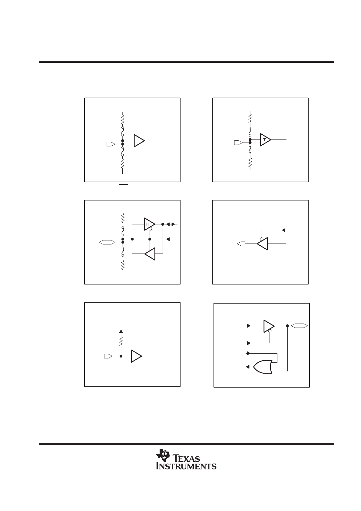
typical input/output schematics
CMOS INPUT (RST/NMI)
I/O WITH SCHMITT-TRIGGER INPUT (P0.x, TP5) CMOS 3-STATE OUTPUT
(TP0–4, XBUF)
V
CC
(see Note A)
(see Note A)
GND
V
CC
(see Note A)
(see Note A)
GND
V
CC
(see Note A)
(see Note A)
GND
V
CC
60 k TYP
MSP430C32x: TMS, TCK, TDI
MSP430P/E325A: TMS, TCK
NOTES: A. Optional selection of pullup or pulldown resistors with ROM (masked) versions. Anti-parallel diodes are connected between A V
SS
and DVSS.
B. Fuses for the optional pullup and pulldown resistors can only be programmed at the factory.
CMOS SCHMITT-TRIGGER INPUT (CIN)
(see Note B)
(see Note B)
(see Note B)
(see Note B)
(see Note B)
(see Note B)
MSP430C32x: TDO/TDI
MSP430P/E325A: TDO/TDI
TDO_Internal
TDO_Control
TDI_Control
TDI_Internal

MSP430C32x, MSP430P325A
MIXED SIGNAL MICROCONTROLLER
SLAS219B – MARCH 1999 – REVISED MARCH 2000
24
POST OFFICE BOX 655303 • DALLAS, TEXAS 75265
TYPICAL CHARACTERISTICS
typical input/output schematics
COM 0–3
VC
VD
Control COM0–3
VA
VB
Segment contol
VA
VB
Segment control
LCDCTL (LCDM5,6,7)
Data (LCD RAM bits 0–3
or bits 4–7)
S0, S1
S2/O2–Sn/On
LCD OUTPUT (COM0–4, Sn, Sn/On)
NOTE: The signals VA, VB, VC, and VD come from the LCD module analog voltage generator.
JTAG Fuse
Blow
Control
TDI/VPP
TDO/TDI
TMS
JTAG
Fuse
VPP_ Internal
TDI_ Internal
TDO/TDI_Control
TDO_ Internal
From/To JTAG_CBT_SIG_REG
NOTES: A. During programming activity and when blowing the JTAG enable fuse, the TDI/VPP terminal is used to apply the correct voltage
source. The TDO/TDI terminal is used to apply the test input data for JTAG circuitry.
B. The TDI/VPP terminal of the ’P325A and ’E325A does not have an internal pullup resistor. An external pulldown resistor is
recommended to avoid a floating node which could increase the current consumption of the device.
C. The TDO/TDI terminal is in a high-impedance state after POR. The ’P325A and ’E325A needs a pullup or a pulldown resistor to avoid
floating a node which could increase the current consumption of the device.
Figure 7. MSP430P325A/E325A: TDI/VPP, TDO/TDI
MSP430C32x, MSP430P325A
MIXED SIGNAL MICROCONTROLLER
SLAS219B – MARCH 1999 – REVISED MARCH 2000
25
POST OFFICE BOX 655303 • DALLAS, TEXAS 75265
TYPICAL CHARACTERISTICS
JTAG fuse check mode
MSP430 devices that have the fuse on the TDI/VPP terminal have a fuse check mode that tests the continuity
of the fuse the first time the JT AG port is accessed after a power-on reset (POR). When activated, a fuse check
current, ITF, of 1 mA at 3 V, 2.5 mA at 5 V can flow from the TDI/VPP pin to ground if the fuse is not burned.
Care must be taken to avoid accidentally activating the fuse check mode and increasing overall system power
consumption.
Activation of the fuse check mode occurs with the first negative edge on the TMS pin after power up or if TMS
is being held low during power up. The second positive edge on the TMS pin deactivates the fuse check mode.
After deactivation, the fuse check mode remains inactive until another POR occurs. After each POR the fuse
check mode has the potential to be activated.
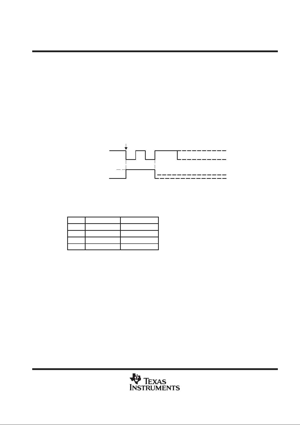
Time TMS Goes Low After POR
TMS
I
TF
I
TDI
Figure 8. Fuse Check Mode Current, MSP430P/E325A, C32x
Care must be taken to avoid accidentally activating the fuse check mode, including guarding against EMI/ESD
spikes that could cause signal edges on the TMS pin.
Configuration of TMS, TCK, TDI/VPP and TDO/TDI pins in applications.
C3xx P/E3xx
TDI Open 68k, pulldown
TDO Open 68k, pulldown
TMS Open Open
TCK Open Open

MSP430C32x, MSP430P325A
MIXED SIGNAL MICROCONTROLLER
SLAS219B – MARCH 1999 – REVISED MARCH 2000
26
POST OFFICE BOX 655303 • DALLAS, TEXAS 75265
MECHANICAL DATA
PG (R-PQFP-G64) PLASTIC QUAD FLATPACK
4040101/B 03/95
0,15 NOM
18,0014,20
13,80 17,20
32
33
20
19
12,00 TYP
0,25
1,10
0,70
0,10 MIN
Gage Plane
51
1
18,00 TYP
52
64
23,60
24,40
19,80
20,20
3,10 MAX
2,70 TYP
0,25
0,45
0°–10°
Seating Plane
0,10
1,00
M
0,20
NOTES: A. All linear dimensions are in millimeters.
B. This drawing is subject to change without notice.
C. Contact field sales office to determine if a tighter coplanarity requirement is available for this package.

MSP430C32x, MSP430P325A
MIXED SIGNAL MICROCONTROLLER
SLAS219B – MARCH 1999 – REVISED MARCH 2000
27
POST OFFICE BOX 655303 • DALLAS, TEXAS 75265
MECHANICAL DATA
pinning MSP43C323, MSP430C325, MSP430P325A (PM package)
1718 19
S19/O19
S18/O18
S17/O17
S16/O16
S15/O15
S14/O14
S13/O13
S12/O12
S11/O11
S10/O10
S9/O9
S8/O8
S7/O7
S6/O6
S5/O5
S4/O4
48
47
46
45
44
43
42
41
40
39
38
37
36
35
34
33
20
1
2
3
4
5
6
7
8
9
10
11
12
13
14
15
16
DV
CC
SV
CC
Rext
A2
A3
A4
A5
Xin
Xout/TCLK
CIN
TP0.0
TP0.1
TP0.2
TP0.3
TP0.4
TP0.5
21 22 23 24
COM0
TDO/TDI
63 62 61 60 5964 58
AVA1A0
XBUF
RST/NMI
TCK
TMS
R32
R13
R03
S0
P0.2/TXD
P0.3
P0.4
P0.5
P0.6
P0.7
R33
56 55 5457
25 26 27 28 29
53 52
P0.0
COM3
COM2
51 50 49
30 31 32
S1
S2/O2
S3/O3
COM1
TDI/
S20/O20/CMPI
AV
DV
P0.1/RXD
SS
SS
CC
PM PACKAGE
(TOP VIEW)
V
PP

MSP430C32x, MSP430P325A
MIXED SIGNAL MICROCONTROLLER
SLAS219B – MARCH 1999 – REVISED MARCH 2000
28
POST OFFICE BOX 655303 • DALLAS, TEXAS 75265
MECHANICAL DATA
PM (S-PQFP-G64) PLASTIC QUAD FLATPACK
4040152/C 11/96
32
17
0,13 NOM
0,25
0,45
0,75
Seating Plane
0,05 MIN
Gage Plane
0,27
33
16
48
1
0,17
49
64
SQ
SQ
10,20
11,80
12,20
9,80
7,50 TYP
1,60 MAX
1,45
1,35
0,08
0,50
M
0,08
0°–7°
NOTES: A. All linear dimensions are in millimeters.
B. This drawing is subject to change without notice.
C. Falls within JEDEC MS-026
D. May also be thermally enhanced plastic with leads connected to the die pads.

MSP430C32x, MSP430P325A
MIXED SIGNAL MICROCONTROLLER
SLAS219B – MARCH 1999 – REVISED MARCH 2000
29
POST OFFICE BOX 655303 • DALLAS, TEXAS 75265
MECHANICAL DATA
pinning MSP43C323, MSP430C325, MSP430P325A (FN package)
28 29
S20/O20/CMPI
S19/O19
S18/O18
S17/O17
S16/O16
S15/O15
S14/O14
S13/O13
S12/O12
S11/O11
S10/O10
S9/O9
S8/O8
S7/O7
S6/O6
S5/O5
S4/O4
60
59
58
57
56
55
54
53
52
51
50
49
48
47
46
45
44
30
10
11
12
13
14
15
16
17
18
19
20
21
22
23
24
25
26
DV
CC
SV
CC
Rext
A2
A3
A4
A5
Xin
Xout/TCLK
CIN
TP0.0
TP0.1
TP0.2
TP0.3
TP0.4
TP0.5
P0.0
31 32 33 34
FN PACKAGE
(TOP VIEW)
TMS
TDI/VPP
87 6 5493
A1A0XBUF
RST/NMI
TCK
R23
R13
R03
S0
P0.2/TXD
P0.3
P0.4
P0.5
P0.6
P0.7
R33
168672
35 36 37 38 39
66 65
27
NC
P0.1/RXD
TDO/TDI
COM3
64 63 62 61
40 41 42 43
S1
S2/O2
S3/O3
NC
COM2
COM1
COM0
NC
NC
AV
SS
DV
SS
AV
CC
NC – No internal connection

MSP430C32x, MSP430P325A
MIXED SIGNAL MICROCONTROLLER
SLAS219B – MARCH 1999 – REVISED MARCH 2000
30
POST OFFICE BOX 655303 • DALLAS, TEXAS 75265
MECHANICAL DATA
FN (S-PQCC-J**) PLASTIC J-LEADED CHIP CARRIER
4040005/B 03/95
20 PIN SHOWN
0.026 (0,66)
0.032 (0,81)
D2/E2
0.020 (0,51) MIN
0.180 (4,57) MAX
0.120 (3,05)
0.090 (2,29)
D2/E2
0.013 (0,33)
0.021 (0,53)
Seating Plane
MAX
D2/E2
0.219 (5,56)
0.169 (4,29)
0.319 (8,10)
0.469 (11,91)
0.569 (14,45)
0.369 (9,37)
MAX
0.356 (9,04)
0.456 (11,58)
0.656 (16,66)
0.008 (0,20) NOM
1.158 (29,41)
0.958 (24,33)
0.756 (19,20)
0.191 (4,85)
0.141 (3,58)
MIN
0.441 (11,20)
0.541 (13,74)
0.291 (7,39)
0.341 (8,66)
18
19
14
13
D
D1
13
9
E1E
4
8
MINMAXMIN
PINS
**
20
28
44
0.385 (9,78)
0.485 (12,32)
0.685 (17,40)
52
68
84
1.185 (30,10)
0.985 (25,02)
0.785 (19,94)
D/E
0.395 (10,03)
0.495 (12,57)
1.195 (30,35)
0.995 (25,27)
0.695 (17,65)
0.795 (20,19)
NO. OF
D1/E1
0.350 (8,89)
0.450 (11,43)
1.150 (29,21)
0.950 (24,13)
0.650 (16,51)
0.750 (19,05)
0.004 (0,10)
M
0.007 (0,18)
0.050 (1,27)
NOTES: A. All linear dimensions are in inches (millimeters).
B. This drawing is subject to change without notice.
C. Falls within JEDEC MS-018

MSP430C32x, MSP430P325A
MIXED SIGNAL MICROCONTROLLER
SLAS219B – MARCH 1999 – REVISED MARCH 2000
31
POST OFFICE BOX 655303 • DALLAS, TEXAS 75265
pinning PMS430E325A (FZ package)
28 29
S20/O20/CMPI
S19/O19
S18/O18
S17/O17
S16/O16
S15/O15
S14/O14
S13/O13
S12/O12
S11/O11
S10/O10
S9/O9
S8/O8
S7/O7
S6/O6
S5/O5
S4/O4
60
59
58
57
56
55
54
53
52
51
50
49
48
47
46
45
44
30
10
11
12
13
14
15
16
17
18
19
20
21
22
23
24
25
26
DV
CC
SV
CC
rext
A2
A3
A4
A5
Xin
Xout/TCLK
CIN
TP0.0
TP0.1
TP0.2
TP0.3
TP0.4
TP0.5
P0.0
31 32 33 34
FZ PACKAGE
(TOP VIEW)
TMS
TDI/
87 6 5493
XBUF
A1
A0
RST/NMI
TCK
R23
R13
R03
S0
P0.2/TXD
P0.3
P0.4
P0.5
P0.6
P0.7
R33
168672
35 36 37 38 39
66 65
27
NC
P0.1/RXD
COM3
COM2
64 63 62 61
40 41 42 43
S1
S2/O2
S3/O3
NC
NC
AV
NC
NC – No internal connection
CC
AV
SS
DV
SS
COM1
COM0
TDO/TDI
Vpp

MSP430C32x, MSP430P325A
MIXED SIGNAL MICROCONTROLLER
SLAS219B – MARCH 1999 – REVISED MARCH 2000
32
POST OFFICE BOX 655303 • DALLAS, TEXAS 75265
MECHANICAL DATA
FZ (S-CQCC-J**) J-LEADED CERAMIC CHIP CARRIER
4040219/B 03/95
0.180 (4,57)
0.140 (3,55)
C
0.020 (0,51)
0.032 (0,81)
A B
A
B
0.025 (0,64) R TYP
0.026 (0,66)
0.120 (3,05)
0.155 (3,94)
0.014 (0,36)
0.120 (3,05)
0.040 (1,02) MIN
0.090 (2,29)
0.040 (1,02) 45°
A
MIN MAX
0.485
(12,32) (12,57)
0.495
0.455
(11,56)(10,92)
0.430
MAXMIN
BC
MIN MAX
0.410
(10,41) (10,92)
0.430
0.6300.6100.630 0.6550.6950.685
(16,00)(15,49)(16,00) (16,64)(17,65)(17,40)
0.7400.6800.730 0.7650.7950.785
(18,79)(17,28)(18,54) (19,43)(20,19)(19,94)
PINS**
28
44
52
NO. OFJEDEC
MO-087AC
MO-087AB
MO-087AA
OUTLINE
28 LEAD SHOWN
Seating Plane
(at Seating
Plane)
1426
25
19
18
12
11
5
0.050 (1,27)
0.9300.9100.930 0.9550.9950.985
(23,62)(23,11)(23,62) (24,26)(25,27)(25,02)
68MO-087AD
NOTES: A. All linear dimensions are in inches (millimeters).
B. This drawing is subject to change without notice.
C. This package can be hermetically sealed with a ceramic lid using glass frit.

IMPORTANT NOTICE
T exas Instruments and its subsidiaries (TI) reserve the right to make changes to their products or to discontinue
any product or service without notice, and advise customers to obtain the latest version of relevant information
to verify, before placing orders, that information being relied on is current and complete. All products are sold
subject to the terms and conditions of sale supplied at the time of order acknowledgement, including those
pertaining to warranty, patent infringement, and limitation of liability.
TI warrants performance of its semiconductor products to the specifications applicable at the time of sale in
accordance with TI’s standard warranty. Testing and other quality control techniques are utilized to the extent
TI deems necessary to support this warranty. Specific testing of all parameters of each device is not necessarily
performed, except those mandated by government requirements.
CERT AIN APPLICATIONS USING SEMICONDUCTOR PRODUCTS MAY INVOLVE POTENTIAL RISKS OF
DEATH, PERSONAL INJURY, OR SEVERE PROPERTY OR ENVIRONMENTAL DAMAGE (“CRITICAL
APPLICATIONS”). TI SEMICONDUCTOR PRODUCTS ARE NOT DESIGNED, AUTHORIZED, OR
WARRANTED TO BE SUITABLE FOR USE IN LIFE-SUPPORT DEVICES OR SYSTEMS OR OTHER
CRITICAL APPLICATIONS. INCLUSION OF TI PRODUCTS IN SUCH APPLICA TIONS IS UNDERSTOOD T O
BE FULLY AT THE CUSTOMER’S RISK.
In order to minimize risks associated with the customer’s applications, adequate design and operating
safeguards must be provided by the customer to minimize inherent or procedural hazards.
TI assumes no liability for applications assistance or customer product design. TI does not warrant or represent
that any license, either express or implied, is granted under any patent right, copyright, mask work right, or other
intellectual property right of TI covering or relating to any combination, machine, or process in which such
semiconductor products or services might be or are used. TI’s publication of information regarding any third
party’s products or services does not constitute TI’s approval, warranty or endorsement thereof.
Copyright 2000, Texas Instruments Incorporated
 Loading...