

Texas Instruments MSP430F5632, MSP430F5635, MSP430F5638, MSP430F5631, MSP430F5630 User Manual
...Page 1

MSP430F5638, MSP430F5637, MSP430F5636
MSP430F5635, MSP430F5634, MSP430F5633
MSP430F5632, MSP430F5631, MSP430F5630
www.ti.com
SLAS650D –JUNE 2010–REVISED AUGUST 2013
Mixed Signal Microcontroller
Check for
Samples: MSP430F5638, MSP430F5637, MSP430F5636, MSP430F5635, MSP430F5634, MSP430F5633, MSP430F5632, MSP430F5631,
1
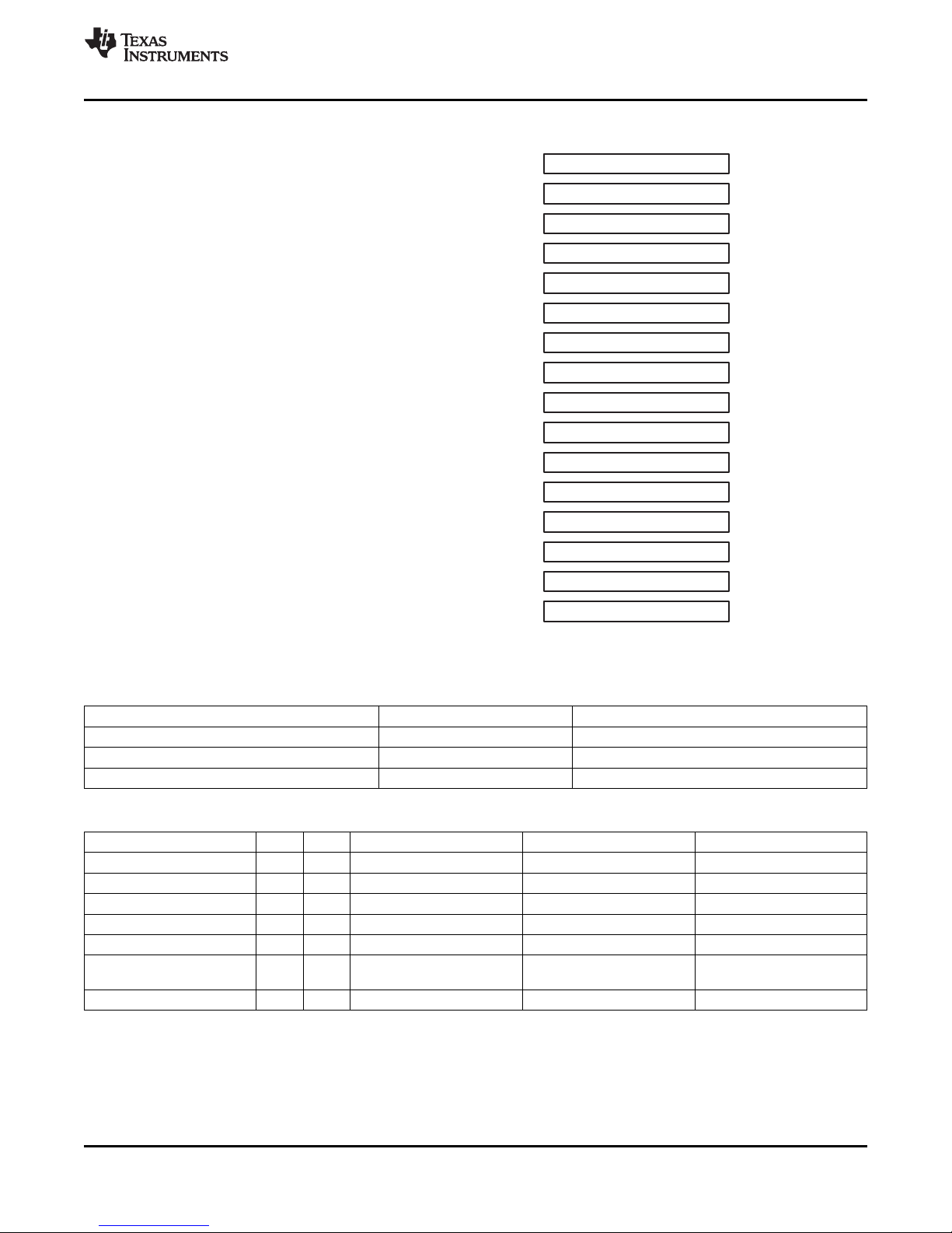
FEATURES
23
• Low Supply Voltage Range: 1.8 V to 3.6 V
• Ultralow-Power Consumption
– Active Mode (AM):
All System Clocks Active:
270 µA/MHz at 8 MHz, 3.0 V, Flash Program – USCI_A0 and USCI_A1 Each Support:
Execution (Typical)
– Standby Mode (LPM3): Baudrate Detection
Watchdog With Crystal and Supply
Supervisor Operational, Full RAM
Retention, Fast Wake-Up:
1.8 µA at 2.2 V, 2.1 µA at 3.0 V (Typical)
– Shutdown RTC Mode (LPM3.5):
Shutdown Mode, Active Real-Time Clock
With Crystal: • Full-Speed Universal Serial Bus (USB)
1.1 µA at 3.0 V (Typical)
– Shutdown Mode (LPM4.5):
0.3 µA at 3.0 V (Typical)
• Wake Up From Standby Mode in 3 µs (Typical)
• 16-Bit RISC Architecture, Extended Memory,
Up to 20-MHz System Clock
• Flexible Power Management System
– Fully Integrated LDO With Programmable and Autoscan Feature
Regulated Core Supply Voltage
– Supply Voltage Supervision, Monitoring, (DACs) With Synchronization
and Brownout
• Unified Clock System
– FLL Control Loop for Frequency Operations
Stabilization
– Low-Power Low-Frequency Internal Clock Programming Voltage Needed
Source (VLO)
– Low-Frequency Trimmed Internal Reference
Source (REFO)
– 32-kHz Crystals (XT1)
– High-Frequency Crystals Up to 32 MHz
(XT2)
MSP430F5630
• Four 16-Bit Timers With 3, 5, or 7
Capture/Compare Registers
• Two Universal Serial Communication
Interfaces
– Enhanced UART Supports Auto-
– IrDA Encoder and Decoder
– Synchronous SPI
– USCI_B0 and USCI_B1 Each Support:
– I2C
– Synchronous SPI
– Integrated USB-PHY
– Integrated 3.3-V and 1.8-V USB Power
System
– Integrated USB-PLL
– Eight Input and Eight Output Endpoints
• 12-Bit Analog-to-Digital Converter (ADC) With
Internal Shared Reference, Sample-and-Hold,
• Dual 12-Bit Digital-to-Analog Converters
• Voltage Comparator
• Hardware Multiplier Supporting 32-Bit
• Serial Onboard Programming, No External
• Six-Channel Internal DMA
• Real-Time Clock Module With Supply Voltage
Backup Switch
• Family Members are Summarized in Table 1
• For Complete Module Descriptions, See the
MSP430x5xx and MSP430x6xx Family User's
Guide (SLAU208)
1
Please be aware that an important notice concerning availability, standard warranty, and use in critical applications of
Texas Instruments semiconductor products and disclaimers thereto appears at the end of this data sheet.
2MSP430, Code Composer Studio are trademarks of Texas Instruments.
3All other trademarks are the property of their respective owners.
PRODUCTION DATA information is current as of publication date.
Products conform to specifications per the terms of the Texas
Instruments standard warranty. Production processing does not
necessarily include testing of all parameters.
Copyright © 2010–2013, Texas Instruments Incorporated
Page 2
MSP430F5638, MSP430F5637, MSP430F5636
MSP430F5635, MSP430F5634, MSP430F5633
MSP430F5632, MSP430F5631, MSP430F5630
SLAS650D –JUNE 2010–REVISED AUGUST 2013
APPLICATIONS
• Analog and Digital Sensor Systems
• Digital Motor Control
• Remote Controls
• Thermostats
• Digital Timers
• Hand-Held Meters
DESCRIPTION
The Texas Instruments MSP430™ family of ultralow-power microcontrollers consists of several devices featuring
different sets of peripherals targeted for various applications. The architecture, combined with five low-power
modes, is optimized to achieve extended battery life in portable measurement applications. The device features a
powerful 16-bit RISC CPU, 16-bit registers, and constant generators that contribute to maximum code efficiency.
The digitally controlled oscillator (DCO) allows the device to wake up from low-power modes to active mode in
3 µs (typical).
The MSP430F563x series are microcontroller configurations with a high-performance 12-bit analog-to-digital
converter (ADC), comparator, two universal serial communication interfaces (USCIs), USB 2.0, a hardware
multiplier, DMA, four 16-bit timers, a real-time clock module with alarm capabilities, and up to 74 I/O pins.
Typical applications for this device include analog and digital sensor systems, digital motor control, remote
controls, thermostats, digital timers, and hand-held meters.
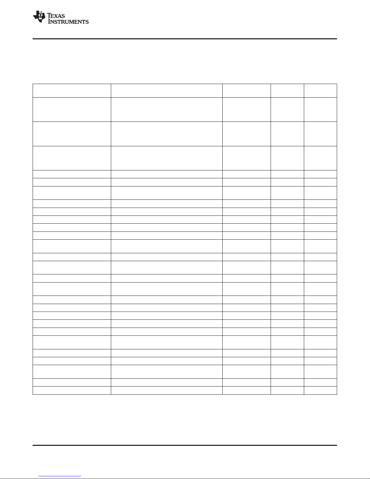
Table 1 summarizes the available family members.
www.ti.com
SPI, I2C
(1)(2)
(Ch) (Ch) (Ch) Type
12 ext, 100 PZ,
4 int 113 ZQW
12 ext, 100 PZ,
4 int 113 ZQW
12 ext, 100 PZ,
4 int 113 ZQW
12 ext, 100 PZ,
4 int 113 ZQW
12 ext, 100 PZ,
4 int 113 ZQW
12 ext, 100 PZ,
4 int 113 ZQW
I/O
100 PZ,
113 ZQW
100 PZ,
113 ZQW
100 PZ,
113 ZQW
Table 1. Family Members
USCI
Device Timer_A
MSP430F5638 256 16 + 2 5, 3, 3 7 2 2 2 12 74
MSP430F5637 192 16 + 2 5, 3, 3 7 2 2 2 12 74
MSP430F5636 128 16 + 2 5, 3, 3 7 2 2 2 12 74
MSP430F5635 256 16 + 2 5, 3, 3 7 2 2 - 12 74
MSP430F5634 192 16 + 2 5, 3, 3 7 2 2 - 12 74
MSP430F5633 128 16 + 2 5, 3, 3 7 2 2 - 12 74
MSP430F5632 256 16 + 2 5, 3, 3 7 2 2 - - 12 74
MSP430F5631 192 16 + 2 5, 3, 3 7 2 2 - - 12 74
MSP430F5630 128 16 + 2 5, 3, 3 7 2 2 - - 12 74
(1) For the most current package and ordering information, see the Package Option Addendum at the end of this document, or see the TI
web site at http://www.ti.com.
(2) Package drawings, standard packing quantities, thermal data, symbolization, and PCB design guidelines are available at
http://www.ti.com/packaging.
(3) The additional 2 KB USB SRAM that is listed can be used as general purpose SRAM when USB is not in use.
(4) Each number in the sequence represents an instantiation of Timer_A with its associated number of capture compare registers and PWM
output generators available. For example, a number sequence of 3, 5 would represent two instantiations of Timer_A, the first
instantiation having 3 and the second instantiation having 5 capture compare registers and PWM output generators, respectively.
(5) Each number in the sequence represents an instantiation of Timer_B with its associated number of capture compare registers and PWM
output generators available. For example, a number sequence of 3, 5 would represent two instantiations of Timer_B, the first
instantiation having 3 and the second instantiation having 5 capture compare registers and PWM output generators, respectively.
Flash SRAM ADC12_A DAC12_A Comp_B Package
(KB) (KB)
(3)
(4)
Timer_B
(5)
Channel A: Channel B:
UART,
IrDA, SPI
2 Submit Documentation Feedback Copyright © 2010–2013, Texas Instruments Incorporated
Product Folder Links: MSP430F5638 MSP430F5637 MSP430F5636 MSP430F5635 MSP430F5634 MSP430F5633
MSP430F5632 MSP430F5631 MSP430F5630
Page 3
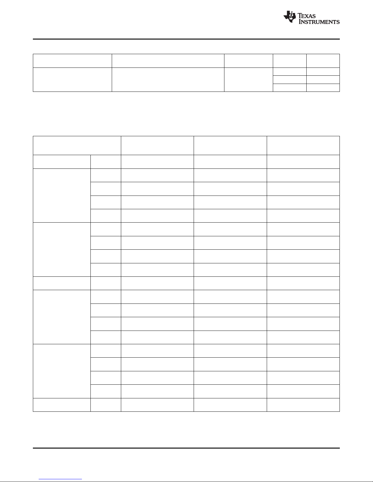
Unified
Clock
System
256KB
192KB
128KB
Flash
16KB
RAM
+2KBRAM
USBBuffer
+8BBackup
RAM
MCLK
ACLK
SMCLK
I/OPorts
P1/P2
2×8I/Os
Interrupt
Capability
PA
1×16I/Os
CPUXV2
and
Working
Registers
EEM
(L:8+2)
XIN
XOUT
JTAG/
Interface/
PortPJ
SBW
PA PB PC PD
DMA
6Channel
XT2IN
XT OUT2
Power
Management
LDO
SVM/
Brownout
SVS
SYS
Watchdog
P2Port
Mapping
Controller
I/OPorts
P3/P4
2×8I/Os
Interrupt
Capability
PB
1×16I/Os
I/OPorts
P5/P6
2×8I/Os
PC
1×16I/Os
I/OPorts
P7/P8
1×6I/Os
PD
1×14I/Os
1×8I/Os
I/OPorts
P9
1×8I/Os
PE
1×8I/Os
MPY32
TA0
Timer_A
5CC
Registers
TA1and
TA2
2Timer_A
eachwith
3CC
Registers
TB0
Timer_B
7CC
Registers
CRC16
USCI0,1
Ax:UART,
IrDA,SPI
Bx:SPI,I2C
ADC12_A
200KSPS
16Channels
(12ext/4int)
Autoscan
12Bit
DVCCDVSSAVCCAV
SS
P1.x P2.x
P3.x
P4.x
P5.x P6.x
P7.x
P8.x P9.x
RST/NMI
REF
Reference
1.5V,2.0V,
2.5V
USB
Full-speed
Comp_B
PJ.x
RTC_B
Battery
Backup
System
Unified
Clock
System
256KB
192KB
128KB
Flash
MCLK
ACLK
SMCLK
I/OPorts
P1/P2
2×8I/Os
Interrupt
Capability
PA
1×16I/Os
CPUXV2
and
Working
Registers
EEM
(L:8+2)
XIN
XOUT
JTAG/
Interface/
PortPJ
SBW
PA PB PC PD
DMA
6Channel
XT2IN
XT OUT2
Power
Management
LDO
SVM/
Brownout
SVS
SYS
Watchdog
P2Port
Mapping
Controller
I/OPorts
P3/P4
2×8I/Os
Interrupt
Capability
PB
1×16I/Os
I/OPorts
P5/P6
2×8I/Os
PC
1×16I/Os
I/OPorts
P7/P8
1×6I/Os
PD
1×14I/Os
1×8I/Os
I/OPorts
P9
1×8I/Os
PE
1×8I/Os
MPY32
TA0
Timer_A
5CC
Registers
TA1and
TA2
2Timer_A
eachwith
3CC
Registers
TB0
Timer_B
7CC
Registers
RTC_B
Battery
Backup
System
CRC16
USCI0,1
Ax:UART,
IrDA,SPI
Bx:SPI,I2C
ADC12_A
200KSPS
16Channels
(12ext/4int)
Autoscan
12Bit
DVCCDVSSAVCCAV
SS
P1.x P2.x
P3.x
P4.x
P5.x P6.x
P7.x
P8.x P9.x
RST/NMI
REF
Reference
1.5V,2.0V,
2.5V
DAC12_A
12bit
2channels
voltageout
USB
Full-speed
Comp_B
PJ.x
16KB
RAM
+2KBRAM
USBBuffer
+8BBackup
RAM
MSP430F5638, MSP430F5637, MSP430F5636
MSP430F5635, MSP430F5634, MSP430F5633
MSP430F5632, MSP430F5631, MSP430F5630
www.ti.com
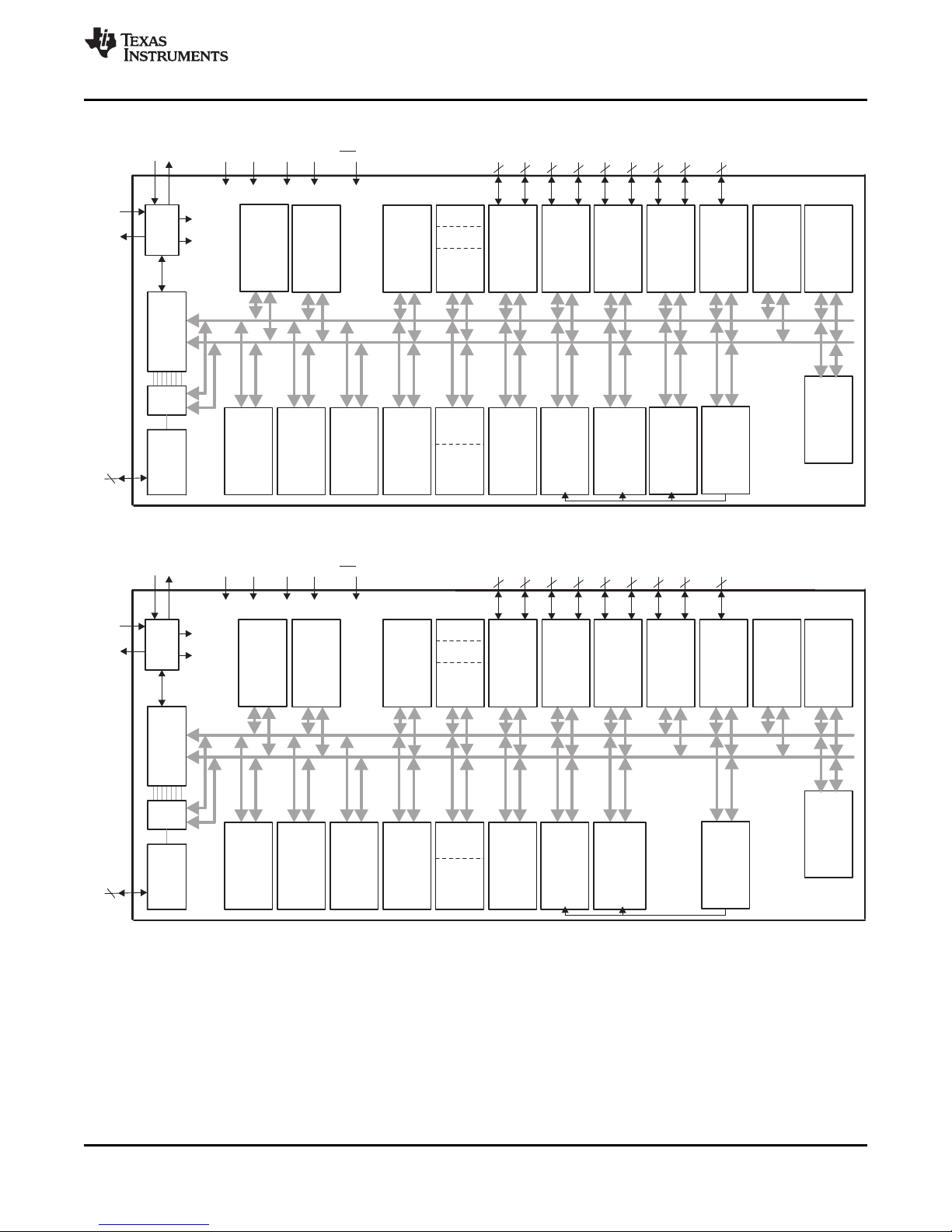
Functional Block Diagram, MSP430F5638, MSP430F5637, MSP430F5636
SLAS650D –JUNE 2010–REVISED AUGUST 2013
Functional Block Diagram, MSP430F5635, MSP430F5634, MSP430F5633
Copyright © 2010–2013, Texas Instruments Incorporated Submit Documentation Feedback 3
Product Folder Links: MSP430F5638 MSP430F5637 MSP430F5636 MSP430F5635 MSP430F5634 MSP430F5633
MSP430F5632 MSP430F5631 MSP430F5630
Page 4

Unified
Clock
System
256KB
192KB
128KB
Flash
MCLK
ACLK
SMCLK
I/OPorts
P1/P2
2×8I/Os
Interrupt
Capability
PA
1×16I/Os
CPUXV2
and
Working
Registers
EEM
(L:8+2)
XIN
XOUT
JTAG/
Interface/
PortPJ
SBW
PA PB PC PD
DMA
6Channel
XT2IN
XT OUT2
Power
Management
LDO
SVM/
Brownout
SVS
SYS
Watchdog
P2Port
Mapping
Controller
I/OPorts
P3/P4
2×8I/Os
Interrupt
Capability
PB
1×16I/Os
I/OPorts
P5/P6
2×8I/Os
PC
1×16I/Os
I/OPorts
P7/P8
1×6I/Os
PD
1×14I/Os
1×8I/Os
I/OPorts
P9
1×8I/Os
PE
1×8I/Os
MPY32
TA0
Timer_A
5CC
Registers
TA1and
TA2
2Timer_A
eachwith
3CC
Registers
TB0
Timer_B
7CC
Registers
CRC16
USCI0,1
Ax:UART,
IrDA,SPI
Bx:SPI,I2C
DVCCDVSSAVCCAV
SS
P1.x P2.x
P3.x
P4.x
P5.x P6.x
P7.x
P8.x P9.x
RST/NMI
REF
Reference
1.5V,2.0V,
2.5V
USB
Full-speed
Comp_B
PJ.x
RTC_B
Battery
Backup
System
16KB
RAM
+2KBRAM
USBBuffer
+8BBackup
RAM
MSP430F5638, MSP430F5637, MSP430F5636
MSP430F5635, MSP430F5634, MSP430F5633
MSP430F5632, MSP430F5631, MSP430F5630
SLAS650D –JUNE 2010–REVISED AUGUST 2013
Functional Block Diagram, MSP430F5632, MSP430F5631, MSP430F5630
www.ti.com
4 Submit Documentation Feedback Copyright © 2010–2013, Texas Instruments Incorporated
Product Folder Links: MSP430F5638 MSP430F5637 MSP430F5636 MSP430F5635 MSP430F5634 MSP430F5633
MSP430F5632 MSP430F5631 MSP430F5630
Page 5
1
2
3
4
5
6
7
8
9
10
11
12
13
14
15
16
17
18
19
20
21
22
23
24
25
76
77
78
79
80
81
82
83
84
85
86
87
88
89
90
91
92
93
94
95
96
97
98
99
100
75
74
73
72
71
70
69
68
67
66
65
64
63
62
61
60
59
58
57
56
55
54
53
52
51
50
49
48
47
46
45
44
43
42
41
40
39
38
37
36
35
34
33
32
31
30
29
28
27
26
P6.4/CB4/A4
P6.5/CB5/A5
P6.6/CB6/A6/DAC0
P6.7/CB7/A7/DAC1
P7.4/CB8/A12
P7.5/CB9/A13
P7.6/CB10/A14/DAC0
P7.7/CB11/A15/DAC1
P5.0/VREF+/VeREF+
P5.1/VREF−/VeREF−
AVCC1
AVSS1
XIN
XOUT
DVCC1
DVSS1
VCORE
P5.2
DVSS
DNC
P5.3
P9.7
P9.6
P9.5
P9.4
P9.3
P9.2
P9.1
P9.0
P8.7
P8.6/UCB1SOMI/UCB1SCL
P8.5/UCB1SIMO/UCB1SDA
DVCC2
DVSS2
P2.0/P2MAP0
MSP430F5638
MSP430F5637
MSP430F5636
PZPACKAGE
(TOP VIEW)
P6.3/CB3/A3
P6.2/CB2/A2
P6.1/CB1/A1
P6.0/CB0/A0
RST/NMI/SBWTDIO
PJ.3/TCK
PJ.2/TMS
PJ.1/TDI/TCLK
PJ.0/TDO
TEST/SBWTCK
P7.3/XT2OUT
P7.2/XT2IN
VBUS
VUSB
PU.1/DM
PUR
PU.0/DP
VSSU
V18
AVSS3
P1.3/TA0.2
P1.4/TA0.3
AVSS2
P5.6/ADC12CLK/DMAE0
P5.4
P5.5
P1.0/TA0CLK/ACLK
P3.0/TA1CLK/CBOUT
P3.1/TA1.0
P3.2/TA1.1
P1.6/TA0.1
P1.7/TA0.2
P1.1/TA0.0
P1.2/TA0.1
P1.5/TA0.4
P3.3/TA1.2
P3.4/TA2CLK/SMCLK
P3.5/TA2.0
P3.6/TA2.1
P3.7/TA2.2
P4.0/TB0.0
P4.2/TB0.2
P4.1/TB0.1
P4.4/TB0.4
P4.3/TB0.3
P4.6/TB0.6
P4.5/TB0.5
P8.0/TB0CLK
P4.7/TB0OUTH/SVMOUT
P8.4/UCB1CLK/UCA1STE
VBAK
P2.1/P2MAP1
P2.2/P2MAP2
P2.3/P2MAP3
P2.4/P2MAP4
P2.5/P2MAP5
P2.6/P2MAP6
P2.7/P2MAP7
DVCC3
DVSS3
VBAT
P5.7/RTCCLK
P8.1/UCB1STE/UCA1CLK
P8.2/UCA1TXD/UCA1SIMO
P8.3/UCA1RXD/UCA1SOMI
MSP430F5638, MSP430F5637, MSP430F5636
MSP430F5635, MSP430F5634, MSP430F5633
MSP430F5632, MSP430F5631, MSP430F5630
www.ti.com
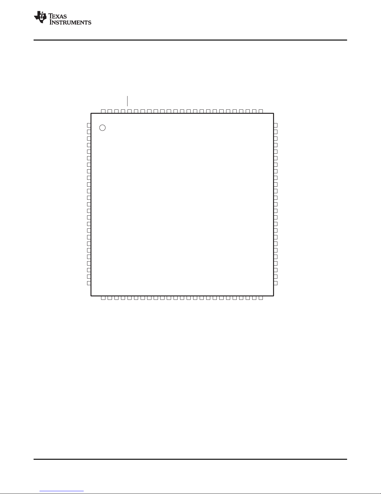
Pin Designation, MSP430F5638IPZ, MSP430F5637IPZ, MSP430F5636IPZ
SLAS650D –JUNE 2010–REVISED AUGUST 2013
NOTE: DNC = Do not connect
Copyright © 2010–2013, Texas Instruments Incorporated Submit Documentation Feedback 5
Product Folder Links: MSP430F5638 MSP430F5637 MSP430F5636 MSP430F5635 MSP430F5634 MSP430F5633
MSP430F5632 MSP430F5631 MSP430F5630
Page 6
1
2
3
4
5
6
7
8
9
10
11
12
13
14
15
16
17
18
19
20
21
22
23
24
25
76
77
78
79
80
81
82
83
84
85
86
87
88
89
90
91
92
93
94
95
96
97
98
99
100
75
74
73
72
71
70
69
68
67
66
65
64
63
62
61
60
59
58
57
56
55
54
53
52
51
50
49
48
47
46
45
44
43
42
41
40
39
38
37
36
35
34
33
32
31
30
29
28
27
26
P6.4/CB4/A4
P6.5/CB5/A5
P6.6/CB6/A6
P6.7/CB7/A7
P7.4/CB8/A12
P7.5/CB9/A13
P7.6/CB10/A14
P7.7/CB11/A15
P5.0/VREF+/VeREF+
P5.1/VREF−/VeREF−
AVCC1
AVSS1
XIN
XOUT
DVCC1
DVSS1
VCORE
P5.2
DVSS
DNC
P5.3
P9.7
P9.6
P9.5
P9.4
P9.3
P9.2
P9.1
P9.0
P8.7
P8.6/UCB1SOMI/UCB1SCL
P8.5/UCB1SIMO/UCB1SDA
DVCC2
DVSS2
P2.0/P2MAP0
MSP430F5635
MSP430F5634
MSP430F5633
PZPACKAGE
(TOP VIEW)
P6.3/CB3/A3
P6.2/CB2/A2
P6.1/CB1/A1
P6.0/CB0/A0
RST/NMI/SBWTDIO
PJ.3/TCK
PJ.2/TMS
PJ.1/TDI/TCLK
PJ.0/TDO
TEST/SBWTCK
P7.3/XT2OUT
P7.2/XT2IN
VBUS
VUSB
PU.1/DM
PUR
PU.0/DP
VSSU
V18
AVSS3
P1.3/TA0.2
P1.4/TA0.3
AVSS2
P5.6/ADC12CLK/DMAE0
P5.4
P5.5
P1.0/TA0CLK/ACLK
P3.0/TA1CLK/CBOUT
P3.1/TA1.0
P3.2/TA1.1
P1.6/TA0.1
P1.7/TA0.2
P1.1/TA0.0
P1.2/TA0.1
P1.5/TA0.4
P3.3/TA1.2
P3.4/TA2CLK/SMCLK
P3.5/TA2.0
P3.6/TA2.1
P3.7/TA2.2
P4.0/TB0.0
P4.2/TB0.2
P4.1/TB0.1
P4.4/TB0.4
P4.3/TB0.3
P4.6/TB0.6
P4.5/TB0.5
P8.0/TB0CLK
P4.7/TB0OUTH/SVMOUT
P8.4/UCB1CLK/UCA1STE
VBAK
P2.1/P2MAP1
P2.2/P2MAP2
P2.3/P2MAP3
P2.4/P2MAP4
P2.5/P2MAP5
P2.6/P2MAP6
P2.7/P2MAP7
DVCC3
DVSS3
VBAT
P5.7/RTCCLK
P8.1/UCB1STE/UCA1CLK
P8.2/UCA1TXD/UCA1SIMO
P8.3/UCA1RXD/UCA1SOMI
MSP430F5638, MSP430F5637, MSP430F5636
MSP430F5635, MSP430F5634, MSP430F5633
MSP430F5632, MSP430F5631, MSP430F5630
SLAS650D –JUNE 2010–REVISED AUGUST 2013
Pin Designation, MSP430F5635IPZ, MSP430F5634IPZ, MSP430F5633IPZ
www.ti.com
NOTE: DNC = Do not connect
6 Submit Documentation Feedback Copyright © 2010–2013, Texas Instruments Incorporated
Product Folder Links: MSP430F5638 MSP430F5637 MSP430F5636 MSP430F5635 MSP430F5634 MSP430F5633
MSP430F5632 MSP430F5631 MSP430F5630
Page 7
1
2
3
4
5
6
7
8
9
10
11
12
13
14
15
16
17
18
19
20
21
22
23
24
25
76
77
78
79
80
81
82
83
84
85
86
87
88
89
90
91
92
93
94
95
96
97
98
99
100
75
74
73
72
71
70
69
68
67
66
65
64
63
62
61
60
59
58
57
56
55
54
53
52
51
50
49
48
47
46
45
44
43
42
41
40
39
38
37
36
35
34
33
32
31
30
29
28
27
26
P6.4/CB4
P6.5/CB5
P6.6/CB6
P6.7/CB7
P7.4/CB8
P7.5/CB9
P7.6/CB10
P7.7/CB11
P5.0/VREF+/VeREF+
P5.1/VREF−/VeREF−
AVCC1
AVSS1
XIN
XOUT
DVCC1
DVSS1
VCORE
P5.2
DVSS
DNC
P5.3
P9.7
P9.6
P9.5
P9.4
P9.3
P9.2
P9.1
P9.0
P8.7
P8.6/UCB1SOMI/UCB1SCL
P8.5/UCB1SIMO/UCB1SDA
DVCC2
DVSS2
P2.0/P2MAP0
MSP430F5632
MSP430F5631
MSP430F5630
PZPACKAGE
(TOP VIEW)
P6.3/CB3
P6.2/CB2
P6.1/CB1
P6.0/CB0
RST/NMI/SBWTDIO
PJ.3/TCK
PJ.2/TMS
PJ.1/TDI/TCLK
PJ.0/TDO
TEST/SBWTCK
P7.3/XT2OUT
P7.2/XT2IN
VBUS
VUSB
PU.1/DM
PUR
PU.0/DP
VSSU
V18
AVSS3
P1.3/TA0.2
P1.4/TA0.3
AVSS2
P5.6/DMAE0
P5.4
P5.5
P1.0/TA0CLK/ACLK
P3.0/TA1CLK/CBOUT
P3.1/TA1.0
P3.2/TA1.1
P1.6/TA0.1
P1.7/TA0.2
P1.1/TA0.0
P1.2/TA0.1
P1.5/TA0.4
P3.3/TA1.2
P3.4/TA2CLK/SMCLK
P3.5/TA2.0
P3.6/TA2.1
P3.7/TA2.2
P4.0/TB0.0
P4.2/TB0.2
P4.1/TB0.1
P4.4/TB0.4
P4.3/TB0.3
P4.6/TB0.6
P4.5/TB0.5
P8.0/TB0CLK
P4.7/TB0OUTH/SVMOUT
P8.4/UCB1CLK/UCA1STE
VBAK
P2.1/P2MAP1
P2.2/P2MAP2
P2.3/P2MAP3
P2.4/P2MAP4
P2.5/P2MAP5
P2.6/P2MAP6
P2.7/P2MAP7
DVCC3
DVSS3
VBAT
P5.7/RTCCLK
P8.1/UCB1STE/UCA1CLK
P8.2/UCA1TXD/UCA1SIMO
P8.3/UCA1RXD/UCA1SOMI
MSP430F5638, MSP430F5637, MSP430F5636
MSP430F5635, MSP430F5634, MSP430F5633
MSP430F5632, MSP430F5631, MSP430F5630
www.ti.com
Pin Designation, MSP430F5632IPZ, MSP430F5631IPZ, MSP430F5630IPZ
SLAS650D –JUNE 2010–REVISED AUGUST 2013
NOTE: DNC = Do not connect
Copyright © 2010–2013, Texas Instruments Incorporated Submit Documentation Feedback 7
Product Folder Links: MSP430F5638 MSP430F5637 MSP430F5636 MSP430F5635 MSP430F5634 MSP430F5633
MSP430F5632 MSP430F5631 MSP430F5630
Page 8
A1 A2
A3
A4
A5 A6
A7
A8 A9 A10
A11 A12
B1 B2
B3
B4
B5 B6
B7
B8 B9 B10
B11 B12
C1 C2 C3 C11 C12
D1 D2 D4
D5 D6
D7
D8 D9
D11 D12
E1 E2 E4
E5 E6
E7
E8 E9
E11 E12
F1 F2 F4
F5 F8 F9
F11 F12
G1 G2 G4
G5 G8 G9
G11 G12
J1 J2 J4
J5 J6
J7
J8 J9
J11 J12
H1 H2 H4
H5 H6
H7
H8 H9
H11 H12
K1 K2 K11 K12
L1 L2
L3
L4
L5 L6
L7
L8 L9 L10
L11 L12
M1 M2
M3 M5 M6
M7
M8 M9 M10
M11 M12
M4
ZQWPACKAGE
(TOP VIEW)
MSP430F5638, MSP430F5637, MSP430F5636
MSP430F5635, MSP430F5634, MSP430F5633
MSP430F5632, MSP430F5631, MSP430F5630
SLAS650D –JUNE 2010–REVISED AUGUST 2013
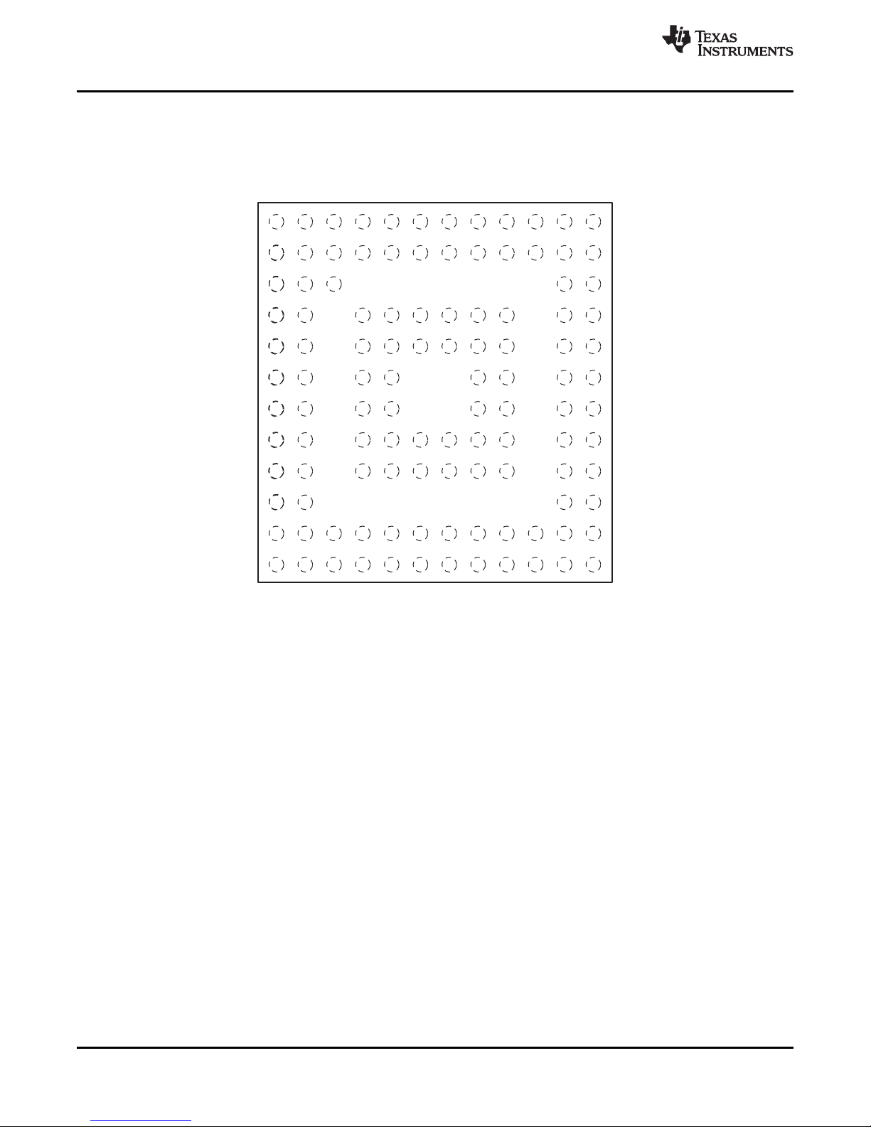
Pin Designation, MSP430F5638IZQW, MSP430F5637IZQW, MSP430F5636IZQW,
MSP430F5635IZQW, MSP430F5634IZQW, MSP430F5633IZQW, MSP430F5632IZQW,
MSP430F5631IZQW, MSP430F5630IZQW
www.ti.com
NOTE: For terminal assignments, see Table 2
8 Submit Documentation Feedback Copyright © 2010–2013, Texas Instruments Incorporated
Product Folder Links: MSP430F5638 MSP430F5637 MSP430F5636 MSP430F5635 MSP430F5634 MSP430F5633
MSP430F5632 MSP430F5631 MSP430F5630
Page 9
MSP430F5638, MSP430F5637, MSP430F5636
MSP430F5635, MSP430F5634, MSP430F5633
MSP430F5632, MSP430F5631, MSP430F5630
www.ti.com
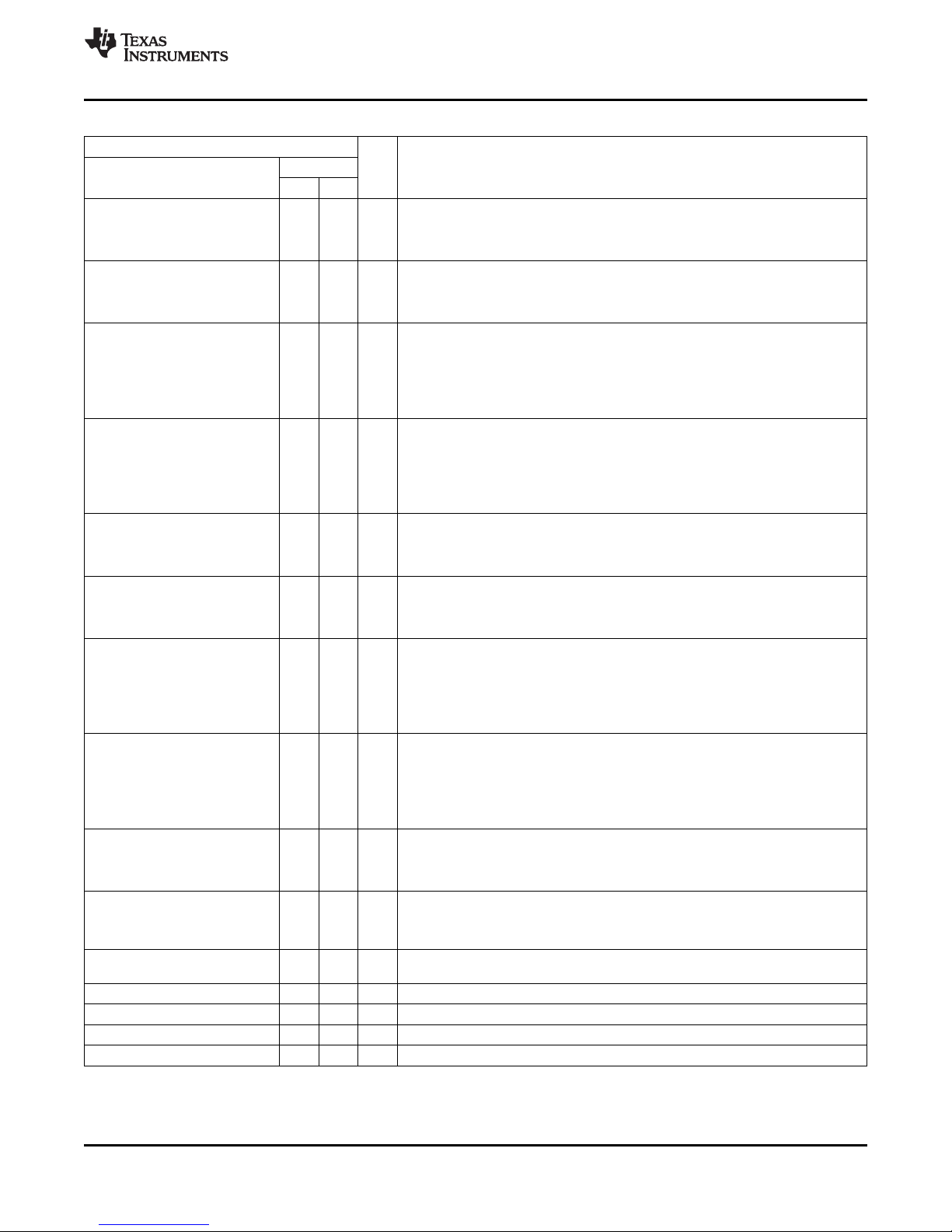
Table 2. Terminal Functions
TERMINAL
NAME
P6.4/CB4/A4 1 A1 I/O
P6.5/CB5/A5 2 B2 I/O
P6.6/CB6/A6/DAC0 3 B1 I/O
P6.7/CB7/A7/DAC1 4 C2 I/O
P7.4/CB8/A12 5 C1 I/O
P7.5/CB9/A13 6 C3 I/O
P7.6/CB10/A14/DAC0 7 D2 I/O
P7.7/CB11/A15/DAC1 8 D1 I/O
P5.0/VREF+/VeREF+ 9 D4 I/O
P5.1/VREF-/VeREF- 10 E4 I/O
AVCC1 11 Analog power supply
AVSS1 12 F2 Analog ground supply
XIN 13 F1 I Input terminal for crystal oscillator XT1
XOUT 14 G1 O Output terminal of crystal oscillator XT1
AVSS2 15 G2 Analog ground supply
NO. I/O
PZ ZQW
E1,
E2
(1)
General-purpose digital I/O
Comparator_B input CB4
Analog input A4 – ADC(not available on F5632, F5631, F5630 devices)
General-purpose digital I/O
Comparator_B input CB5
Analog input A5 – ADC(not available on F5632, F5631, F5630 devices)
General-purpose digital I/O
Comparator_B input CB6
Analog input A6 – ADC (not available on F5632, F5631, F5630 devices)
DAC12.0 output (not available on F5635, F5634, F5633, F5632, F5631, F5630
devices)
General-purpose digital I/O
Comparator_B input CB7
Analog input A7 – ADC (not available on F5632, F5631, F5630 devices)
DAC12.1 output (not available on F5635, F5634, F5633, F5632, F5631, F5630
devices)
General-purpose digital I/O
Comparator_B input CB8
Analog input A12 –ADC (not available on F5632, F5631, F5630 devices)
General-purpose digital I/O
Comparator_B input CB9
Analog input A13 – ADC (not available on F5632, F5631, F5630 devices)
General-purpose digital I/O
Comparator_B input CB10
Analog input A14 – ADC (not available on F5632, F5631, F5630 devices)
DAC12.0 output (not available on F5635, F5634, F5633, F5632, F5631, F5630
devices)
General-purpose digital I/O
Comparator_B input CB11
Analog input A15 – ADC (not available on F5632, F5631, F5630 devices)
DAC12.1 output (not available on F5635, F5634, F5633, F5632, F5631, F5630
devices)
General-purpose digital I/O
Output of reference voltage to the ADC
Input for an external reference voltage to the ADC
General-purpose digital I/O
Negative terminal for the ADC's reference voltage for both sources, the internal
reference voltage, or an external applied reference voltage
DESCRIPTION
SLAS650D –JUNE 2010–REVISED AUGUST 2013
(1) I = input, O = output, N/A = not available on this package offering
Copyright © 2010–2013, Texas Instruments Incorporated Submit Documentation Feedback 9
Product Folder Links: MSP430F5638 MSP430F5637 MSP430F5636 MSP430F5635 MSP430F5634 MSP430F5633
MSP430F5632 MSP430F5631 MSP430F5630
Page 10
MSP430F5638, MSP430F5637, MSP430F5636
MSP430F5635, MSP430F5634, MSP430F5633
MSP430F5632, MSP430F5631, MSP430F5630
SLAS650D –JUNE 2010–REVISED AUGUST 2013
Table 2. Terminal Functions (continued)
TERMINAL
NAME
P5.6/ADC12CLK/DMAE0 16 H1 I/O
P2.0/P2MAP0 17 G4 I/O
P2.1/P2MAP1 18 H2 I/O
P2.2/P2MAP2 19 J1 I/O
P2.3/P2MAP3 20 H4 I/O
P2.4/P2MAP4 21 J2 I/O
P2.5/P2MAP5 22 K1 I/O
P2.6/P2MAP6 23 K2 I/O
P2.7/P2MAP7 24 L2 I/O
DVCC1 25 L1 Digital power supply
DVSS1 26 M1 Digital ground supply
(2)
VCORE
P5.2 28 L3 I/O
DVSS 29 M3 Digital ground supply
DNC 30 J4 Do not connect. It is strongly recommended to leave this terminal open.
P5.3 31 L4 I/O
P5.4 32 M4 I/O
P5.5 33 J5 I/O
P1.0/TA0CLK/ACLK 34 L5 I/O
P1.1/TA0.0 35 M5 I/O
P1.2/TA0.1 36 J6 I/O
P1.3/TA0.2 37 H6 I/O
P1.4/TA0.3 38 M6 I/O
NO. I/O
PZ ZQW
27 M2 Regulated core power supply (internal use only, no external current loading)
(1)
General-purpose digital I/O
Conversion clock output ADC (not available on F5632, F5631, F5630 devices)
DMA external trigger input
General-purpose digital I/O with port interrupt and mappable secondary function
Default mapping: USCI_B0 SPI slave transmit enable; USCI_A0 clock input/output
General-purpose digital I/O with port interrupt and mappable secondary function
Default mapping: USCI_B0 SPI slave in/master out; USCI_B0 I2C data
General-purpose digital I/O with port interrupt and mappable secondary function
Default mapping: USCI_B0 SPI slave out/master in; USCI_B0 I2C clock
General-purpose digital I/O with port interrupt and mappable secondary function
Default mapping: USCI_B0 clock input/output; USCI_A0 SPI slave transmit enable
General-purpose digital I/O with port interrupt and mappable secondary function
Default mapping: USCI_A0 UART transmit data; USCI_A0 SPI slave in/master out
General-purpose digital I/O with port interrupt and mappable secondary function
Default mapping: USCI_A0 UART receive data; USCI_A0 slave out/master in
General-purpose digital I/O with port interrupt and mappable secondary function
Default mapping: no secondary function
General-purpose digital I/O with port interrupt and mappable secondary function
Default mapping: no secondary function
General-purpose digital I/O
General-purpose digital I/O
General-purpose digital I/O
General-purpose digital I/O
General-purpose digital I/O with port interrupt
Timer TA0 clock signal TACLK input
ACLK output (divided by 1, 2, 4, 8, 16, or 32)
General-purpose digital I/O with port interrupt
Timer TA0 CCR0 capture: CCI0A input, compare: Out0 output
BSL transmit output
General-purpose digital I/O with port interrupt
Timer TA0 CCR1 capture: CCI1A input, compare: Out1 output
BSL receive input
General-purpose digital I/O with port interrupt
Timer TA0 CCR2 capture: CCI2A input, compare: Out2 output
General-purpose digital I/O with port interrupt
Timer TA0 CCR3 capture: CCI3A input compare: Out3 output
DESCRIPTION
www.ti.com
(2) VCORE is for internal use only. No external current loading is possible. VCORE should only be connected to the recommended
capacitor value, C
10 Submit Documentation Feedback Copyright © 2010–2013, Texas Instruments Incorporated
Product Folder Links: MSP430F5638 MSP430F5637 MSP430F5636 MSP430F5635 MSP430F5634 MSP430F5633
VCORE
.
MSP430F5632 MSP430F5631 MSP430F5630
Page 11
www.ti.com
Table 2. Terminal Functions (continued)
TERMINAL
NAME
P1.5/TA0.4 39 L6 I/O
P1.6/TA0.1 40 J7 I/O
P1.7/TA0.2 41 M7 I/O
P3.0/TA1CLK/CBOUT 42 L7 I/O
P3.1/TA1.0 43 H7 I/O
P3.2/TA1.1 44 M8 I/O
P3.3/TA1.2 45 L8 I/O
P3.4/TA2CLK/SMCLK 46 J8 I/O
P3.5/TA2.0 47 M9 I/O
P3.6/TA2.1 48 L9 I/O
P3.7/TA2.2 49 M10 I/O
P4.0/TB0.0 50 J9 I/O
P4.1/TB0.1 51 M11 I/O
P4.2/TB0.2 52 L10 I/O
P4.3/TB0.3 53 M12 I/O
P4.4/TB0.4 54 L12 I/O
P4.5/TB0.5 55 L11 I/O
P4.6/TB0.6 56 K11 I/O
P4.7/TB0OUTH/SVMOUT 57 K12 I/O
P8.0/TB0CLK 58 J11 I/O
NO. I/O
PZ ZQW
MSP430F5638, MSP430F5637, MSP430F5636
MSP430F5635, MSP430F5634, MSP430F5633
MSP430F5632, MSP430F5631, MSP430F5630
SLAS650D –JUNE 2010–REVISED AUGUST 2013
(1)
General-purpose digital I/O with port interrupt
Timer TA0 CCR4 capture: CCI4A input, compare: Out4 output
General-purpose digital I/O with port interrupt
Timer TA0 CCR1 capture: CCI1B input, compare: Out1 output
General-purpose digital I/O with port interrupt
Timer TA0 CCR2 capture: CCI2B input, compare: Out2 output
General-purpose digital I/O with port interrupt
Timer TA1 clock input
Comparator_B output
General-purpose digital I/O with port interrupt
Timer TA1 capture CCR0: CCI0A/CCI0B input, compare: Out0 output
General-purpose digital I/O with port interrupt
Timer TA1 capture CCR1: CCI1A/CCI1B input, compare: Out1 output
General-purpose digital I/O with port interrupt
Timer TA1 capture CCR2: CCI2A/CCI2B input, compare: Out2 output
General-purpose digital I/O with port interrupt
Timer TA2 clock input
SMCLK output
General-purpose digital I/O with port interrupt
Timer TA2 capture CCR0: CCI0A/CCI0B input, compare: Out0 output
General-purpose digital I/O with port interrupt
Timer TA2 capture CCR1: CCI1A/CCI1B input, compare: Out1 output
General-purpose digital I/O with port interrupt
Timer TA2 capture CCR2: CCI2A/CCI2B input, compare: Out2 output
General-purpose digital I/O with port interrupt
Timer TB0 capture CCR0: CCI0A/CCI0B input, compare: Out0 output
General-purpose digital I/O with port interrupt
Timer TB0 capture CCR1: CCI1A/CCI1B input, compare: Out1 output
General-purpose digital I/O with port interrupt
Timer TB0 capture CCR2: CCI2A/CCI2B input, compare: Out2 output
General-purpose digital I/O with port interrupt
Timer TB0 capture CCR3: CCI3A/CCI3B input, compare: Out3 output
General-purpose digital I/O with port interrupt
Timer TB0 capture CCR4: CCI4A/CCI4B input, compare: Out4 output
General-purpose digital I/O with port interrupt
Timer TB0 capture CCR5: CCI5A/CCI5B input, compare: Out5 output
General-purpose digital I/O with port interrupt
Timer TB0 capture CCR6: CCI6A/CCI6B input, compare: Out6 output
General-purpose digital I/O with port interrupt
Timer TB0: Switch all PWM outputs high impedance
SVM output
General-purpose digital I/O
Timer TB0 clock input
DESCRIPTION
Copyright © 2010–2013, Texas Instruments Incorporated Submit Documentation Feedback 11
Product Folder Links: MSP430F5638 MSP430F5637 MSP430F5636 MSP430F5635 MSP430F5634 MSP430F5633
MSP430F5632 MSP430F5631 MSP430F5630
Page 12
MSP430F5638, MSP430F5637, MSP430F5636
MSP430F5635, MSP430F5634, MSP430F5633
MSP430F5632, MSP430F5631, MSP430F5630
SLAS650D –JUNE 2010–REVISED AUGUST 2013
Table 2. Terminal Functions (continued)
TERMINAL
NAME
P8.1/UCB1STE/UCA1CLK 59 J12 I/O
P8.2/UCA1TXD/UCA1SIMO 60 H11 I/O
P8.3/UCA1RXD/UCA1SOMI 61 H12 I/O
P8.4/UCB1CLK/UCA1STE 62 G11 I/O
DVSS2 63 G12 Digital ground supply
DVCC2 64 F12 Digital power supply
P8.5/UCB1SIMO/UCB1SDA 65 F11 I/O
P8.6/UCB1SOMI/UCB1SCL 66 G9 I/O
P8.7 67 E12 I/O
P9.0 68 E11 I/O
P9.1 69 F9 I/O
P9.2 70 D12 I/O
P9.3 71 D11 I/O
P9.4 72 E9 I/O
P9.5 73 C12 I/O
P9.6 74 C11 I/O
P9.7 75 D9 I/O
VSSU 76 and USB PHY ground supply
PU.0/DP 77 A12 I/O
PUR 78 B10 I/O invoke the default USB BSL. Recommended 1-MΩ resistor to ground. See USB
PU.1/DM 79 A11 I/O
VBUS 80 A10 USB LDO input (connect to USB power source)
VUSB 81 A9 USB LDO output
V18 82 B9 USB regulated power (internal use only, no external current loading)
AVSS3 83 A8 Analog ground supply
P7.2/XT2IN 84 B8 I/O
P7.3/XT2OUT 85 B7 I/O
VBAK 86 A7
NO. I/O
PZ ZQW
B11
B12
(1)
General-purpose digital I/O
USCI_B1 SPI slave transmit enable; USCI_A1 clock input/output
General-purpose digital I/O
USCI_A1 UART transmit data; USCI_A1 SPI slave in/master out
General-purpose digital I/O
USCI_A1 UART receive data; USCI_A1 SPI slave out/master in
General-purpose digital I/O
USCI_B1 clock input/output; USCI_A1 SPI slave transmit enable
General-purpose digital I/O
USCI_B1 SPI slave in/master out; USCI_B1 I2C data
General-purpose digital I/O
USCI_B1 SPI slave out/master in; USCI_B1 I2C clock
General-purpose digital I/O
General-purpose digital I/O
General-purpose digital I/O
General-purpose digital I/O
General-purpose digital I/O
General-purpose digital I/O
General-purpose digital I/O
General-purpose digital I/O
General-purpose digital I/O
General-purpose digital I/O - controlled by USB control register
USB data terminal DP
USB pullup resistor pin (open drain). The voltage level at the PUR pin is used to
BSL for more information.
General-purpose digital I/O - controlled by USB control register
USB data terminal DM
General-purpose digital I/O
Input terminal for crystal oscillator XT2
General-purpose digital I/O
Output terminal of crystal oscillator XT2
Capacitor for backup subsystem. Do not load this pin externally. For capacitor
values, see C
in Recommended Operating Conditions.
BAK
DESCRIPTION
www.ti.com
12 Submit Documentation Feedback Copyright © 2010–2013, Texas Instruments Incorporated
Product Folder Links: MSP430F5638 MSP430F5637 MSP430F5636 MSP430F5635 MSP430F5634 MSP430F5633
MSP430F5632 MSP430F5631 MSP430F5630
Page 13
MSP430F5638, MSP430F5637, MSP430F5636
MSP430F5635, MSP430F5634, MSP430F5633
MSP430F5632, MSP430F5631, MSP430F5630
www.ti.com
Table 2. Terminal Functions (continued)
TERMINAL
NAME
VBAT 87 D8
P5.7/RTCCLK 88 D7 I/O
DVCC3 89 A6 Digital power supply
DVSS3 90 A5 Digital ground supply
TEST/SBWTCK 91 B6 I
PJ.0/TDO 92 B5 I/O
PJ.1/TDI/TCLK 93 A4 I/O
PJ.2/TMS 94 E7 I/O
PJ.3/TCK 95 D6 I/O
RST/NMI/SBWTDIO 96 A3 I/O
P6.0/CB0/A0 97 B4 I/O
P6.1/CB1/A1 98 B3 I/O
P6.2/CB2/A2 99 A2 I/O
P6.3/CB3/A3 100 D5 I/O
Reserved N/A F8, Reserved. It is recommended to connect to ground (DVSS, AVSS).
(3) When this pin is configured as reset, the intermal pullup resistor is enabled by default.
NO. I/O
PZ ZQW
E5,
E6,
E8,
F4,
F5,
G5,
G8,
H5,
H8,
H9
(1)
Backup or secondary supply voltage. If backup voltage is not supplied, connect to
DVCC externally.
General-purpose digital I/O
RTCCLK output
Test mode pin; selects digital I/O on JTAG pins
Spy-bi-wire input clock
General-purpose digital I/O
Test data output port
General-purpose digital I/O
Test data input or test clock input
General-purpose digital I/O
Test mode select
General-purpose digital I/O
Test clock
Reset input (active low)
Non-maskable interrupt input
Spy-bi-wire data input/output
General-purpose digital I/O
Comparator_B input CB0
Analog input A0 – ADC (not available on F5632, F5631, F5630 devices)
General-purpose digital I/O
Comparator_B input CB1
Analog input A1 – ADC (not available on F5632, F5631, F5630 devices)
General-purpose digital I/O
Comparator_B input CB2
Analog input A2 – ADC (not available on F5632, F5631, F5630 devices)
General-purpose digital I/O
Comparator_B input CB3
Analog input A3 – ADC (not available on F5632, F5631, F5630 devices)
(3)
SLAS650D –JUNE 2010–REVISED AUGUST 2013
DESCRIPTION
Copyright © 2010–2013, Texas Instruments Incorporated Submit Documentation Feedback 13
Product Folder Links: MSP430F5638 MSP430F5637 MSP430F5636 MSP430F5635 MSP430F5634 MSP430F5633
MSP430F5632 MSP430F5631 MSP430F5630
Page 14
MSP430F5638, MSP430F5637, MSP430F5636
MSP430F5635, MSP430F5634, MSP430F5633
MSP430F5632, MSP430F5631, MSP430F5630
SLAS650D –JUNE 2010–REVISED AUGUST 2013
Development Tools Support
All MSP430™ microcontrollers are supported by a wide variety of software and hardware development tools.
Tools are available from TI and various third parties. See them all at www.ti.com/msp430tools.
Hardware Features
See the Code Composer Studio for MSP430 User's Guide (SLAU157) for details on the available features.
www.ti.com
MSP430 4-Wire 2-Wire Clock State Trace
Architecture JTAG JTAG Control Sequencer Buffer
MSP430Xv2 Yes Yes 8 Yes Yes Yes Yes No
Break- Range LPMx.5
points Break- Debugging
(N) points Support
Recommended Hardware Options
Target Socket Boards
The target socket boards allow easy programming and debugging of the device using JTAG. They also feature
header pin outs for prototyping. Target socket boards are orderable individually or as a kit with the JTAG
programmer and debugger included. The following table shows the compatible target boards and the supported
packages.
Package Target Board and Programmer Bundle Target Board Only
100-pin LQFP (PZ) MSP-FET430U100USB MSP-TS430PZ100USB
Experimenter Boards
Experimenter Boards and Evaluation kits are available for some MSP430 devices. These kits feature additional
hardware components and connectivity for full system evaluation and prototyping. See www.ti.com/msp430tools
for details.
Debugging and Programming Tools
Hardware programming and debugging tools are available from TI and from its third party suppliers. See the full
list of available tools at www.ti.com/msp430tools.
Production Programmers
The production programmers expedite loading firmware to devices by programming several devices
simultaneously.
Part Number PC Port Features Provider
MSP-GANG Serial and USB Program up to eight devices at a time. Works with PC or standalone. Texas Instruments
Recommended Software Options
Integrated Development Environments
Software development tools are available from TI or from third parties. Open source solutions are also available.
This device is supported by Code Composer Studio™ IDE (CCS).
MSP430Ware
MSP430Ware is a collection of code examples, data sheets, and other design resources for all MSP430 devices
delivered in a convenient package. In addition to providing a complete collection of existing MSP430 design
resources, MSP430Ware also includes a high-level API called MSP430 Driver Library. This library makes it easy
to program MSP430 hardware. MSP430Ware is available as a component of CCS or as a standalone package.
14 Submit Documentation Feedback Copyright © 2010–2013, Texas Instruments Incorporated
Product Folder Links: MSP430F5638 MSP430F5637 MSP430F5636 MSP430F5635 MSP430F5634 MSP430F5633
MSP430F5632 MSP430F5631 MSP430F5630
Page 15

MSP430F5638, MSP430F5637, MSP430F5636
MSP430F5635, MSP430F5634, MSP430F5633
MSP430F5632, MSP430F5631, MSP430F5630
www.ti.com
TI-RTOS
TI-RTOS is a complete real-time operating system for the MSP430 microcontrollers. It combines a real-time
multitasking kernel SYS/BIOS with additional middleware components. TI-RTOS is available free of charge and
provided with full source code.
MSP430 USB Developer's Package
MSP430 USB Developer's Package is an easy-to-use USB stack implementation for the MSP430
microcontrollers.
Command-Line Programmer
MSP430 Flasher is an open-source, shell-based interface for programming MSP430 microcontrollers through a
FET programmer or eZ430 using JTAG or Spy-Bi-Wire (SBW) communication. MSP430 Flasher can be used to
download binary files (.txt or .hex) files directly to the MSP430 Flash without the need for an IDE.
Community Resources
The following links connect to TI community resources. Linked contents are provided "AS IS" by the respective
contributors. They do not constitute TI specifications and do not necessarily reflect TI's views; see TI's Terms of
Use.
TI E2E Community
TI's Engineer-to-Engineer (E2E) Community. Created to foster collaboration among engineers. At e2e.ti.com, you
can ask questions, share knowledge, explore ideas, and help solve problems with fellow engineers.
TI Embedded Processors Wiki
Texas Instruments Embedded Processors Wiki. Established to help developers get started with embedded
processors from Texas Instruments and to foster innovation and growth of general knowledge about the
hardware and software surrounding these devices.
SLAS650D –JUNE 2010–REVISED AUGUST 2013
Device and Development Tool Nomenclature
To designate the stages in the product development cycle, TI assigns prefixes to the part numbers of all
MSP430™ MCU devices and support tools. Each MSP430™ MCU commercial family member has one of two
prefixes: MSP or XMS (for example, MSP430F5259). Texas Instruments recommends two of three possible
prefix designators for its support tools: MSP and MSPX. These prefixes represent evolutionary stages of product
development from engineering prototypes (with XMS for devices and MSPX for tools) through fully qualified
production devices and tools (with MSP for devices and MSP for tools).
Device development evolutionary flow:
XMS – Experimental device that is not necessarily representative of the final device's electrical specifications
MSP – Fully qualified production device
Support tool development evolutionary flow:
MSPX – Development-support product that has not yet completed Texas Instruments internal qualification
testing.
MSP – Fully-qualified development-support product
XMS devices and MSPX development-support tools are shipped against the following disclaimer:
"Developmental product is intended for internal evaluation purposes."
MSP devices and MSP development-support tools have been characterized fully, and the quality and reliability of
the device have been demonstrated fully. TI's standard warranty applies.
Predictions show that prototype devices (XMS) have a greater failure rate than the standard production devices.
Texas Instruments recommends that these devices not be used in any production system because their
expected end-use failure rate still is undefined. Only qualified production devices are to be used.
Copyright © 2010–2013, Texas Instruments Incorporated Submit Documentation Feedback 15
Product Folder Links: MSP430F5638 MSP430F5637 MSP430F5636 MSP430F5635 MSP430F5634 MSP430F5633
MSP430F5632 MSP430F5631 MSP430F5630
Page 16

Processor Family
CC = Embedded RF Radio
MSP = Mixed Signal Processor
XMS = Experimental Silicon
430 MCU Platform TI’s Low Power Microcontroller Platform
Device Type Memory Type
C = ROM
F = Flash
FR = FRAM
G = Flash (Value Line)
L = No Nonvolatile Memory
Specialized Application
AFE = Analog Front End
BT = Preprogrammed with Bluetooth
BQ = Contactless Power
CG = ROM Medical
FE = Flash Energy Meter
FG = Flash Medical
FW = Flash Electronic Flow Meter
Series 1 Series = Up to 8 MHz
2 Series = Up to 16 MHz
3 Series = Legacy
4 Series = Up to 16 MHz w/ LCD
5 Series = Up to 25 MHz
6 Series = Up to 25 MHz w/ LCD
0 = Low Voltage Series
Feature Set Various Levels of Integration Within a Series
Optional: A = Revision N/A
Optional: Temperature Range S = 0°C to 50 C
C to 70 C
I = -40 C to 85 C
T = -40 C to 105 C
°
C = 0° °
° °
° °
Packaging
www.ti.com/packaging
Optional: Tape and Reel T = Small Reel (7 inch)
R = Large Reel (11 inch)
No Markings = Tube or Tray
Optional: Additional Features *-EP = Enhanced Product (-40°C to 105°C)
*-HT = Extreme Temperature Parts (-55°C to 150°C)
MSP 430 F 5 438 A I ZQW T XX
Processor Family
Series
Optional: Temperature Range
430 MCU Platform
PackagingDevice Type
Optional: A = Revision
Optional: Tape and Reel
Feature Set
Optional: Additional Features
MSP430F5638, MSP430F5637, MSP430F5636
MSP430F5635, MSP430F5634, MSP430F5633
MSP430F5632, MSP430F5631, MSP430F5630
SLAS650D –JUNE 2010–REVISED AUGUST 2013
TI device nomenclature also includes a suffix with the device family name. This suffix indicates the package type
(for example, PZP) and temperature range (for example, T). Figure 1 provides a legend for reading the complete
device name for any family member.
Part Number Decoder
www.ti.com
16 Submit Documentation Feedback Copyright © 2010–2013, Texas Instruments Incorporated
Product Folder Links: MSP430F5638 MSP430F5637 MSP430F5636 MSP430F5635 MSP430F5634 MSP430F5633
Figure 1. Device Nomenclature
MSP430F5632 MSP430F5631 MSP430F5630
Page 17
Program Counter
PC/R0
Stack Pointer SP/R1
Status Register
SR/CG1/R2
Constant Generator CG2/R3
General-Purpose Register
R4
General-Purpose Register
R5
General-Purpose Register
R6
General-Purpose Register
R7
General-Purpose Register
R8
General-Purpose Register
R9
General-Purpose Register
R10
General-Purpose Register
R11
General-Purpose Register
R12
General-Purpose Register
R13
General-Purpose Register
R15
General-Purpose Register
R14
www.ti.com
Short-Form Description
CPU
The MSP430 CPU has a 16-bit RISC architecture
that is highly transparent to the application. All
operations, other than program-flow instructions, are
performed as register operations in conjunction with
seven addressing modes for source operand and four
addressing modes for destination operand.
The CPU is integrated with 16 registers that provide
reduced instruction execution time. The register-toregister operation execution time is one cycle of the
CPU clock.
Four of the registers, R0 to R3, are dedicated as
program counter, stack pointer, status register, and
constant generator, respectively. The remaining
registers are general-purpose registers.
Peripherals are connected to the CPU using data,
address, and control buses, and can be handled with
all instructions.
MSP430F5638, MSP430F5637, MSP430F5636
MSP430F5635, MSP430F5634, MSP430F5633
MSP430F5632, MSP430F5631, MSP430F5630
SLAS650D –JUNE 2010–REVISED AUGUST 2013
Instruction Set
The instruction set consists of the original 51
instructions with three formats and seven address
modes and additional instructions for the expanded
address range. Each instruction can operate on word
and byte data. Table 3 shows examples of the three
types of instruction formats; Table 4 shows the
address modes.
INSTRUCTION WORD FORMAT EXAMPLE OPERATION
Dual operands, source-destination ADD R4,R5 R4 + R5 → R5
Single operands, destination only CALL R8 PC → (TOS), R8 → PC
Relative jump, un/conditional JNE Jump-on-equal bit = 0
ADDRESS MODE S
Register + + MOV Rs,Rd MOV R10,R11 R10 → R11
Indexed + + MOV X(Rn),Y(Rm) MOV 2(R5),6(R6) M(2+R5) → M(6+R6)
Symbolic (PC relative) + + MOV EDE,TONI M(EDE) → M(TONI)
Absolute + + MOV &MEM, &TCDAT M(MEM) → M(TCDAT)
Indirect + MOV @Rn,Y(Rm) MOV @R10,Tab(R6) M(R10) → M(Tab+R6)
Indirect auto-increment + MOV @Rn+,Rm MOV @R10+,R11
Immediate + MOV #X,TONI MOV #45,TONI #45 → M(TONI)
(1) S = source, D = destination
Table 3. Instruction Word Formats
Table 4. Address Mode Descriptions
(1)
(1)
D
SYNTAX EXAMPLE OPERATION
M(R10) → R11
R10 + 2 → R10
Copyright © 2010–2013, Texas Instruments Incorporated Submit Documentation Feedback 17
Product Folder Links: MSP430F5638 MSP430F5637 MSP430F5636 MSP430F5635 MSP430F5634 MSP430F5633
MSP430F5632 MSP430F5631 MSP430F5630
Page 18

MSP430F5638, MSP430F5637, MSP430F5636
MSP430F5635, MSP430F5634, MSP430F5633
MSP430F5632, MSP430F5631, MSP430F5630
SLAS650D –JUNE 2010–REVISED AUGUST 2013
Operating Modes
The MSP430 has one active mode and seven software selectable low-power modes of operation. An interrupt
event can wake up the device from any of the low-power modes, service the request, and restore back to the
low-power mode on return from the interrupt program.
The following seven operating modes can be configured by software:
• Active mode (AM)
– All clocks are active
• Low-power mode 0 (LPM0)
– CPU is disabled
– ACLK and SMCLK remain active, MCLK is disabled
– FLL loop control remains active
• Low-power mode 1 (LPM1)
– CPU is disabled
– FLL loop control is disabled
– ACLK and SMCLK remain active, MCLK is disabled
• Low-power mode 2 (LPM2)
– CPU is disabled
– MCLK, FLL loop control, and DCOCLK are disabled
– DCO's dc generator remains enabled
– ACLK remains active
• Low-power mode 3 (LPM3)
– CPU is disabled
– MCLK, FLL loop control, and DCOCLK are disabled
– DCO's dc generator is disabled
– ACLK remains active
• Low-power mode 4 (LPM4)
– CPU is disabled
– ACLK is disabled
– MCLK, FLL loop control, and DCOCLK are disabled
– DCO's dc generator is disabled
– Crystal oscillator is stopped
– Complete data retention
• Low-power mode 3.5 (LPM3.5)
– Internal regulator disabled
– No data retention
– RTC enabled and clocked by low-frequency oscillator
– Wakeup from RST/NMI, RTC_B, P1, P2, P3, and P4
• Low-power mode 4.5 (LPM4.5)
– Internal regulator disabled
– No data retention
– Wakeup from RST/NMI, RTC_B, P1, P2, P3, and P4
www.ti.com
18 Submit Documentation Feedback Copyright © 2010–2013, Texas Instruments Incorporated
Product Folder Links: MSP430F5638 MSP430F5637 MSP430F5636 MSP430F5635 MSP430F5634 MSP430F5633
MSP430F5632 MSP430F5631 MSP430F5630
Page 19
MSP430F5638, MSP430F5637, MSP430F5636
MSP430F5635, MSP430F5634, MSP430F5633
MSP430F5632, MSP430F5631, MSP430F5630
www.ti.com
Interrupt Vector Addresses
The interrupt vectors and the power-up start address are located in the address range 0FFFFh to 0FF80h. The
vector contains the 16-bit address of the appropriate interrupt-handler instruction sequence.
Table 5. Interrupt Sources, Flags, and Vectors of MSP430F563x Configurations
INTERRUPT SOURCE INTERRUPT FLAG PRIORITY
System Reset
Power-Up, External Reset
Watchdog Timeout, Key Violation
WDTIFG, KEYV (SYSRSTIV)
Flash Memory Key Violation
System NMI
PMM
Vacant Memory Access
JTAG Mailbox
SVMLIFG, SVMHIFG, DLYLIFG, DLYHIFG,
VLRLIFG, VLRHIFG, VMAIFG, JMBNIFG, (Non)maskable 0FFFCh 62
JMBOUTIFG (SYSSNIV)
User NMI
NMI NMIIFG, OFIFG, ACCVIFG, BUSIFG
Oscillator Fault (SYSUNIV)
(1)(2)
Flash Memory Access Violation
Comp_B Comparator B interrupt flags (CBIV)
Timer TB0 TB0CCR0 CCIFG0
Timer TB0 Maskable 0FFF4h 58
TB0CCR1 CCIFG1 to TB0CCR6 CCIFG6,
TB0IFG (TBIV)
Watchdog Interval Timer Mode WDTIFG Maskable 0FFF2h 57
USCI_A0 Receive or Transmit UCA0RXIFG, UCA0TXIFG (UCA0IV)
USCI_B0 Receive or Transmit UCB0RXIFG, UCB0TXIFG (UCB0IV)
ADC12_A
(4)
ADC12IFG0 to ADC12IFG15 (ADC12IV)
Timer TA0 TA0CCR0 CCIFG0
Timer TA0 Maskable 0FFE8h 52
TA0CCR1 CCIFG1 to TA0CCR4 CCIFG4,
TA0IFG (TA0IV)
USB_UBM USB interrupts (USBIV)
DMA Maskable 0FFE4h 50
DMA0IFG, DMA1IFG, DMA2IFG, DMA3IFG,
DMA4IFG, DMA5IFG (DMAIV)
Timer TA1 TA1CCR0 CCIFG0
Timer TA1 Maskable 0FFE0h 48
TA1CCR1 CCIFG1 to TA1CCR2 CCIFG2,
TA1IFG (TA1IV)
I/O Port P1 P1IFG.0 to P1IFG.7 (P1IV)
USCI_A1 Receive or Transmit UCA1RXIFG, UCA1TXIFG (UCA1IV)
USCI_B1 Receive or Transmit UCB1RXIFG, UCB1TXIFG (UCB1IV)
I/O Port P2 P2IFG.0 to P2IFG.7 (P2IV)
Reserved Reserved Maskable 0FFD6h 43
RTC_B Maskable 0FFD4h 42
DAC12_A
(5)
RTCRDYIFG, RTCTEVIFG, RTCAIFG,
RT0PSIFG, RT1PSIFG, RTCOFIFG (RTCIV)
DAC12_0IFG, DAC12_1IFG
Timer TA2 TA2CCR0 CCIFG0
Timer TA2 Maskable 0FFCEh 39
TA2CCR1 CCIFG1 to TA2CCR2 CCIFG2,
TA2IFG (TA2IV)
I/O Port P3 P3IFG.0 to P3IFG.7 (P3IV)
I/O Port P4 P4IFG.0 to P4IFG.7 (P4IV)
(1)(2)
(1)
(1)(3)
(3)
(1) (3)
(1)(3)
(1)(3)
(1)(3)
(3)
(1)(3)
(1)(3)
(1)(3)
(3)
(1)(3)
(1) (3)
(1)(3)
(1)(3)
(1) (3)
(1)(3)
(1)(3)
(3)
(1)(3)
(1)(3)
(1)(3)
SLAS650D –JUNE 2010–REVISED AUGUST 2013
SYSTEM WORD
INTERRUPT ADDRESS
Reset 0FFFEh 63, highest
(Non)maskable 0FFFAh 61
Maskable 0FFF8h 60
Maskable 0FFF6h 59
Maskable 0FFF0h 56
Maskable 0FFEEh 55
Maskable 0FFECh 54
Maskable 0FFEAh 53
Maskable 0FFE6h 51
Maskable 0FFE2h 49
Maskable 0FFDEh 47
Maskable 0FFDCh 46
Maskable 0FFDAh 45
Maskable 0FFD8h 44
Maskable 0FFD2h 41
Maskable 0FFD0h 40
Maskable 0FFCCh 38
Maskable 0FFCAh 37
(1) Multiple source flags
(2) A reset is generated if the CPU tries to fetch instructions from within peripheral space or vacant memory space.
(Non)maskable: the individual interrupt-enable bit can disable an interrupt event, but the general-interrupt enable cannot disable it.
(3) Interrupt flags are located in the module.
(4) Only on devices with peripheral module ADC12_A, otherwise reserved.
(5) Only on devices with peripheral module DAC12_A, otherwise reserved.
Copyright © 2010–2013, Texas Instruments Incorporated Submit Documentation Feedback 19
Product Folder Links: MSP430F5638 MSP430F5637 MSP430F5636 MSP430F5635 MSP430F5634 MSP430F5633
MSP430F5632 MSP430F5631 MSP430F5630
Page 20
MSP430F5638, MSP430F5637, MSP430F5636
MSP430F5635, MSP430F5634, MSP430F5633
MSP430F5632, MSP430F5631, MSP430F5630
SLAS650D –JUNE 2010–REVISED AUGUST 2013
Table 5. Interrupt Sources, Flags, and Vectors of MSP430F563x Configurations (continued)
INTERRUPT SOURCE INTERRUPT FLAG PRIORITY
Reserved Reserved
(6) Reserved interrupt vectors at addresses are not used in this device and can be used for regular program code if necessary. To maintain
compatability with other devices, it is recommended to reserve these locations.
(6)
SYSTEM WORD
INTERRUPT ADDRESS
0FFC8h 36
⋮ ⋮
0FF80h 0, lowest
Memory Organization
www.ti.com
Table 6. Memory Organization
MSP430F5636 MSP430F5637 MSP430F5638
MSP430F5633 MSP430F5634 MSP430F5635
MSP430F5630 MSP430F5631 MSP430F5632
Memory (flash) Total Size 128KB 192KB 256KB
Main: interrupt vector 00FFFFh–00FF80h 00FFFFh–00FF80h 00FFFFh–00FF80h
Bank 3 N/A N/A 64 KB
Bank 2 N/A 64 KB 64 KB
Main: code memory
RAM
USB RAM
Information memory
(flash)
Bootstrap loader (BSL)
memory (flash)
Peripherals
(1) N/A = Not available.
(2) Backup RAM is accessed via the control registers BAKMEM0, BAKMEM1, BAKMEM2, and BAKMEM3.
(3) USB RAM can be used as general purpose RAM when not used for USB operation.
(3)
Bank 1 64 KB 64 KB 64 KB
027FFF-018000h 027FFF-018000h 027FFF-018000h
Bank 0 64 KB 64 KB 64 KB
017FFF-008000h 017FFF-008000h 017FFF-008000h
Sector 3 4 KB 4 KB 4 KB
0063FFh–005400h 0063FFh–005400h 0063FFh–005400h
Sector 2 4 KB 4 KB 4 KB
0053FFh–004400h 0053FFh–004400h 0053FFh–004400h
Sector 1 4 KB 4 KB 4 KB
0043FFh–003400h 0043FFh–003400h 0043FFh–003400h
Sector 0 4 KB 4 KB 4 KB
0033FFh–002400h 0033FFh–002400h 0033FFh–002400h
Size 2KB 2KB 2KB
RAM 0023FFh-001C00h 0023FFh-001C00h 0023FFh-001C00h
Info A 128 B 128 B 128 B
0019FFh–001980h 0019FFh–001980h 0019FFh–001980h
Info B 128 B 128 B 128 B
00197Fh–001900h 00197Fh–001900h 00197Fh–001900h
Info C 128 B 128 B 128 B
0018FFh–001880h 0018FFh–001880h 0018FFh–001880h
Info D 128 B 128 B 128 B
00187Fh–001800h 00187Fh–001800h 00187Fh–001800h
BSL 3 512 B 512 B 512 B
0017FFh–001600h 0017FFh–001600h 0017FFh–001600h
BSL 2 512 B 512 B 512 B
0015FFh–001400h 0015FFh–001400h 0015FFh–001400h
BSL 1 512 B 512 B 512 B
0013FFh–001200h 0013FFh–001200h 0013FFh–001200h
BSL 0 512 B 512 B 512 B
0011FFh–001000h 0011FFh–001000h 0011FFh–001000h
Size 4KB 4KB 4KB
000FFFh–000000h 000FFFh–000000h 000FFFh–000000h
(1)(2)
047FFF-038000h
037FFF-028000h 037FFF-028000h
20 Submit Documentation Feedback Copyright © 2010–2013, Texas Instruments Incorporated
Product Folder Links: MSP430F5638 MSP430F5637 MSP430F5636 MSP430F5635 MSP430F5634 MSP430F5633
MSP430F5632 MSP430F5631 MSP430F5630
Page 21
MSP430F5638, MSP430F5637, MSP430F5636
MSP430F5635, MSP430F5634, MSP430F5633
MSP430F5632, MSP430F5631, MSP430F5630
www.ti.com
Bootstrap Loader (BSL)
The BSL enables users to program the flash memory or RAM using various serial interfaces. Access to the
device memory via the BSL is protected by an user-defined password. For complete description of the features of
the BSL and its implementation, see MSP430 Programming Via the Bootstrap Loader (BSL) (SLAU319).
USB BSL
All devices come pre-programmed with the USB BSL. Use of the USB BSL requires external access to the six
pins shown in Table 7. In addition to these pins, the application must support external components necessary for
normal USB operation; for example, the proper crystal on XT2IN and XT2OUT or proper decoupling.
Table 7. USB BSL Pin Requirements and Functions
DEVICE SIGNAL BSL FUNCTION
RST/NMI/SBWTDIO Entry sequence signal
PU.0/DP USB data terminal DP
PU.1/DM USB data terminal DM
PUR USB pullup resistor terminal
VBUS USB bus power supply
VSSU USB ground supply
SLAS650D –JUNE 2010–REVISED AUGUST 2013
NOTE
The default USB BSL evaluates the logic level of the PUR pin after a BOR reset. If it is
pulled high externally, then the BSL is invoked. Therefore, unless the application is
invoking the BSL, it is important to keep PUR pulled low after a BOR reset, even if BSL or
USB is never used. Applying a 1-MΩ resistor to ground is recommended.
UART BSL
A UART BSL is also available that can be programmed by the user into the BSL memory by replacing the preprogrammed, factory supplied, USB BSL. Use of the UART BSL requires external access to the six pins shown
in Table 8.
Table 8. UART BSL Pin Requirements and Functions
DEVICE SIGNAL BSL FUNCTION
RST/NMI/SBWTDIO Entry sequence signal
TEST/SBWTCK Entry sequence signal
P1.1 Data transmit
P1.2 Data receive
VCC Power supply
VSS Ground supply
JTAG Operation
JTAG Standard Interface
The MSP430 family supports the standard JTAG interface which requires four signals for sending and receiving
data. The JTAG signals are shared with general-purpose I/O. The TEST/SBWTCK pin is used to enable the
JTAG signals. In addition to these signals, the RST/NMI/SBWTDIO is required to interface with MSP430
development tools and device programmers. The JTAG pin requirements are shown in Table 9. For further
details on interfacing to development tools and device programmers, see the MSP430(tm) Hardware Tools
User's Guide (SLAU278). For a complete description of the features of the JTAG interface and its
implementation, see MSP430 Programming Via the JTAG Interface (SLAU320).
Copyright © 2010–2013, Texas Instruments Incorporated Submit Documentation Feedback 21
Product Folder Links: MSP430F5638 MSP430F5637 MSP430F5636 MSP430F5635 MSP430F5634 MSP430F5633
MSP430F5632 MSP430F5631 MSP430F5630
Page 22
MSP430F5638, MSP430F5637, MSP430F5636
MSP430F5635, MSP430F5634, MSP430F5633
MSP430F5632, MSP430F5631, MSP430F5630
SLAS650D –JUNE 2010–REVISED AUGUST 2013
Table 9. JTAG Pin Requirements and Functions
DEVICE SIGNAL DIRECTION FUNCTION
PJ.3/TCK IN JTAG clock input
PJ.2/TMS IN JTAG state control
PJ.1/TDI/TCLK IN JTAG data input, TCLK input
PJ.0/TDO OUT JTAG data output
TEST/SBWTCK IN Enable JTAG pins
RST/NMI/SBWTDIO IN External reset
VCC Power supply
VSS Ground supply
Spy-Bi-Wire Interface
In addition to the standard JTAG interface, the MSP430 family supports the two wire Spy-Bi-Wire interface. SpyBi-Wire can be used to interface with MSP430 development tools and device programmers. The Spy-Bi-Wire
interface pin requirements are shown in Table 10. For further details on interfacing to development tools and
device programmers, see the MSP430(tm) Hardware Tools User's Guide (SLAU278). For a complete description
of the features of the JTAG interface and its implementation, see MSP430 Programming Via the JTAG Interface
(SLAU320).
www.ti.com
Table 10. Spy-Bi-Wire Pin Requirements and Functions
DEVICE SIGNAL DIRECTION FUNCTION
TEST/SBWTCK IN Spy-Bi-Wire clock input
RST/NMI/SBWTDIO IN, OUT Spy-Bi-Wire data input/output
VCC Power supply
VSS Ground supply
Flash Memory (Link to User's Guide)
The flash memory can be programmed via the JTAG port, Spy-Bi-Wire (SBW), the BSL, or in-system by the
CPU. The CPU can perform single-byte, single-word, and long-word writes to the flash memory. Features of the
flash memory include:
• Flash memory has n segments of main memory and four segments of information memory (A to D) of
128 bytes each. Each segment in main memory is 512 bytes in size.
• Segments 0 to n may be erased in one step, or each segment may be individually erased.
• Segments A to D can be erased individually, or as a group with segments 0 to n. Segments A to D are also
called information memory.
• Segment A can be locked separately.
RAM Memory (Link to User's Guide)
The RAM memory is made up of n sectors. Each sector can be completely powered down to save leakage,
however all data is lost. Features of the RAM memory include:
• RAM memory has n sectors. The size of a sector can be found in Memory Organization.
• Each sector 0 to n can be complete disabled, however data retention is lost.
• Each sector 0 to n automatically enters low power retention mode when possible.
• For devices that contain USB memory, the USB memory can be used as normal RAM if USB is not required.
Backup RAM Memory
The backup RAM provides a limited number of bytes of RAM that are retained during LPMx.5 and during
operation from a backup supply if the Battery Backup System module is implemented.
There are 8 bytes of Backup RAM available on MSP430F563x. It can be wordwise accessed via the control
registers BAKMEM0, BAKMEM1, BAKMEM2, and BAKMEM3.
22 Submit Documentation Feedback Copyright © 2010–2013, Texas Instruments Incorporated
Product Folder Links: MSP430F5638 MSP430F5637 MSP430F5636 MSP430F5635 MSP430F5634 MSP430F5633
MSP430F5632 MSP430F5631 MSP430F5630
Page 23
MSP430F5638, MSP430F5637, MSP430F5636
MSP430F5635, MSP430F5634, MSP430F5633
MSP430F5632, MSP430F5631, MSP430F5630
www.ti.com
Peripherals
Peripherals are connected to the CPU through data, address, and control buses and can be handled using all
instructions. For complete module descriptions, see the MSP430x5xx and MSP430x6xx Family User's Guide
(SLAU208).
Digital I/O (Link to User's Guide)
There are up to nine 8-bit I/O ports implemented: P1 through P6, P8, and P9 are complete, P7 contains six
individual I/O ports, and PJ contains four individual I/O ports.
• All individual I/O bits are independently programmable.
• Any combination of input, output, and interrupt conditions is possible.
• Programmable pullup or pulldown on all ports.
• Programmable drive strength on all ports.
• Edge-selectable interrupt input capability for all the eight bits of ports P1, P2, P3, and P4.
• Read/write access to port-control registers is supported by all instructions.
• Ports can be accessed byte-wise (P1 through P9) or word-wise in pairs (PA through PD).
Port Mapping Controller (Link to User's Guide)
The port mapping controller allows the flexible and reconfigurable mapping of digital functions to port P2.
SLAS650D –JUNE 2010–REVISED AUGUST 2013
Table 11. Port Mapping, Mnemonics and Functions
VALUE PxMAPy MNEMONIC INPUT PIN FUNCTION OUTPUT PIN FUNCTION
0 PM_NONE None DV
1
2
3
4 PM_TB0CCR0B Timer TB0 CCR0 capture input CCI0B Timer TB0: TB0.0 compare output Out0
5 PM_TB0CCR1B Timer TB0 CCR1 capture input CCI1B Timer TB0: TB0.1 compare output Out1
6 PM_TB0CCR2B Timer TB0 CCR2 capture input CCI2B Timer TB0: TB0.2 compare output Out2
7 PM_TB0CCR3B Timer TB0 CCR3 capture input CCI3B Timer TB0: TB0.3 compare output Out3
8 PM_TB0CCR4B Timer TB0 CCR4 capture input CCI4B Timer TB0: TB0.4 compare output Out4
9 PM_TB0CCR5B Timer TB0 CCR5 capture input CCI5B Timer TB0: TB0.5 compare output Out5
10 PM_TB0CCR6B Timer TB0 CCR6 capture input CCI6B Timer TB0: TB0.6 compare output Out6
11
12
13
14
15
16
17 PM_MCLK - MCLK
18 Reserved Reserved for test purposes. Do not use this setting.
PM_CBOUT - Comparator_B output
PM_TB0CLK Timer TB0 clock input -
PM_ADC12CLK - ADC12CLK
PM_DMAE0 DMAE0 Input -
PM_SVMOUT - SVM output
PM_TB0OUTH -
PM_UCA0RXD USCI_A0 UART RXD (Direction controlled by USCI - input)
PM_UCA0SOMI USCI_A0 SPI slave out master in (direction controlled by USCI)
PM_UCA0TXD USCI_A0 UART TXD (Direction controlled by USCI - output)
PM_UCA0SIMO USCI_A0 SPI slave in master out (direction controlled by USCI)
PM_UCA0CLK USCI_A0 clock input/output (direction controlled by USCI)
PM_UCB0STE USCI_B0 SPI slave transmit enable (direction controlled by USCI - input)
PM_UCB0SOMI USCI_B0 SPI slave out master in (direction controlled by USCI)
PM_UCB0SCL USCI_B0 I2C clock (open drain and direction controlled by USCI)
PM_UCB0SIMO USCI_B0 SPI slave in master out (direction controlled by USCI)
PM_UCB0SDA USCI_B0 I2C data (open drain and direction controlled by USCI)
PM_UCB0CLK USCI_B0 clock input/output (direction controlled by USCI)
PM_UCA0STE USCI_A0 SPI slave transmit enable (direction controlled by USCI - input)
Timer TB0 high impedance input
TB0OUTH
SS
Copyright © 2010–2013, Texas Instruments Incorporated Submit Documentation Feedback 23
Product Folder Links: MSP430F5638 MSP430F5637 MSP430F5636 MSP430F5635 MSP430F5634 MSP430F5633
MSP430F5632 MSP430F5631 MSP430F5630
Page 24

MSP430F5638, MSP430F5637, MSP430F5636
MSP430F5635, MSP430F5634, MSP430F5633
MSP430F5632, MSP430F5631, MSP430F5630
SLAS650D –JUNE 2010–REVISED AUGUST 2013
Table 11. Port Mapping, Mnemonics and Functions (continued)
VALUE PxMAPy MNEMONIC INPUT PIN FUNCTION OUTPUT PIN FUNCTION
19 Reserved Reserved for test purposes. Do not use this setting.
20-30 Reserved None DVSS
31 (0FFh)
(1) The value of the PM_ANALOG mnemonic is set to 0FFh. The port mapping registers are only 5 bits wide and the upper bits are ignored,
(1)
which results in a read out value of 31.
PM_ANALOG
Disables the output driver and the input Schmitt-trigger to prevent parasitic cross currents
when applying analog signals.
Table 12. Default Mapping
PIN INPUT PIN FUNCTION OUTPUT PIN FUNCTION
P2.0/P2MAP0
P2.1/P2MAP1
P2.2/P2MAP2
P2.3/P2MAP3
P2.4/P2MAP4
P2.5/P2MAP5
P2.6/P2MAP6 PM_NONE - DVSS
P2.7/P2MAP7 PM_NONE - DVSS
PxMAPy
MNEMONIC
PM_UCB0STE, USCI_B0 SPI slave transmit enable (direction controlled by USCI - input),
PM_UCA0CLK USCI_A0 clock input/output (direction controlled by USCI)
PM_UCB0SIMO, USCI_B0 SPI slave in master out (direction controlled by USCI),
PM_UCB0SDA USCI_B0 I2C data (open drain and direction controlled by USCI)
PM_UCB0SOMI, USCI_B0 SPI slave out master in (direction controlled by USCI),
PM_UCB0SCL USCI_B0 I2C clock (open drain and direction controlled by USCI)
PM_UCB0CLK, USCI_B0 clock input/output (direction controlled by USCI),
PM_UCA0STE USCI_A0 SPI slave transmit enable (direction controlled by USCI - input)
PM_UCA0TXD, USCI_A0 UART TXD (direction controlled by USCI - output),
PM_UCA0SIMO USCI_A0 SPI slave in master out (direction controlled by USCI)
PM_UCA0RXD, USCI_A0 UART RXD (direction controlled by USCI - input),
PM_UCA0SOMI USCI_A0 SPI slave out master in (direction controlled by USCI)
www.ti.com
Oscillator and System Clock (Link to User's Guide)
The clock system in the MSP430F563x family of devices is supported by the Unified Clock System (UCS)
module that includes support for a 32-kHz watch crystal oscillator (in XT1 LF mode; XT1 HF mode is not
supported), an internal very-low-power low-frequency oscillator (VLO), an internal trimmed low-frequency
oscillator (REFO), an integrated internal digitally controlled oscillator (DCO), and a high-frequency crystal
oscillator XT2. The UCS module is designed to meet the requirements of both low system cost and low power
consumption. The UCS module features digital frequency locked loop (FLL) hardware that, in conjunction with a
digital modulator, stabilizes the DCO frequency to a programmable multiple of the watch crystal frequency. The
internal DCO provides a fast turn-on clock source and stabilizes in 3 µs (typical). The UCS module provides the
following clock signals:
• Auxiliary clock (ACLK), sourced from a 32-kHz watch crystal (XT1), a high-frequency crystal (XT2), the
internal low-frequency oscillator (VLO), the trimmed low-frequency oscillator (REFO), or the internal digitallycontrolled oscillator DCO.
• Main clock (MCLK), the system clock used by the CPU. MCLK can be sourced by same sources available to
ACLK.
• Sub-Main clock (SMCLK), the subsystem clock used by the peripheral modules. SMCLK can be sourced by
same sources available to ACLK.
• ACLK/n, the buffered output of ACLK, ACLK/2, ACLK/4, ACLK/8, ACLK/16, ACLK/32.
Power Management Module (PMM) (Link to User's Guide)
The PMM includes an integrated voltage regulator that supplies the core voltage to the device and contains
programmable output levels to provide for power optimization. The PMM also includes supply voltage supervisor
(SVS) and supply voltage monitoring (SVM) circuitry, as well as brownout protection. The brownout circuit is
implemented to provide the proper internal reset signal to the device during power-on and power-off. The SVS
and SVM circuitry detects if the supply voltage drops below a user-selectable level and supports both supply
voltage supervision (the device is automatically reset) and supply voltage monitoring (the device is not
automatically reset). SVS and SVM circuitry is available on the primary supply and core supply.
24 Submit Documentation Feedback Copyright © 2010–2013, Texas Instruments Incorporated
Product Folder Links: MSP430F5638 MSP430F5637 MSP430F5636 MSP430F5635 MSP430F5634 MSP430F5633
MSP430F5632 MSP430F5631 MSP430F5630
Page 25

MSP430F5638, MSP430F5637, MSP430F5636
MSP430F5635, MSP430F5634, MSP430F5633
MSP430F5632, MSP430F5631, MSP430F5630
www.ti.com
Hardware Multiplier (MPY) (Link to User's Guide)
The multiplication operation is supported by a dedicated peripheral module. The module performs operations with
32-bit, 24-bit, 16-bit, and 8-bit operands. The module is capable of supporting signed and unsigned multiplication
as well as signed and unsigned multiply and accumulate operations.
Real-Time Clock (RTC_B) (Link to User's Guide)
The RTC_B module can be configured for real-time clock (RTC) or calendar mode providing seconds, minutes,
hours, day of week, day of month, month, and year. Calendar mode integrates an internal calendar which
compensates for months with less than 31 days and includes leap year correction. The RTC_B also supports
flexible alarm functions and offset-calibration hardware. The implementation on this device supports operation in
LPM3.5 mode and operation from a backup supply.
Watchdog Timer (WDT_A) (Link to User's Guide)
The primary function of the watchdog timer (WDT_A) module is to perform a controlled system restart after a
software problem occurs. If the selected time interval expires, a system reset is generated. If the watchdog
function is not needed in an application, the module can be configured as an interval timer and can generate
interrupts at selected time intervals.
System Module (SYS) (Link to User's Guide)
The SYS module handles many of the system functions within the device. These include power-on reset and
power-up clear handling, NMI source selection and management, reset interrupt vector generators, bootstrap
loader entry mechanisms, and configuration management (device descriptors). SYS also includes a data
exchange mechanism via JTAG called a JTAG mailbox that can be used in the application.
SLAS650D –JUNE 2010–REVISED AUGUST 2013
Table 13. System Module Interrupt Vector Registers
INTERRUPT VECTOR
REGISTER
SYSRSTIV, System Reset 019Eh
INTERRUPT EVENT WORD ADDRESS OFFSET PRIORITY
No interrupt pending 00h
Brownout (BOR) 02h Highest
RST/NMI (BOR) 04h
DoBOR (BOR) 06h
LPM3.5 or LPM4.5 wakeup (BOR) 08h
Security violation (BOR) 0Ah
SVSL (POR) 0Ch
SVSH (POR) 0Eh
SVML_OVP (POR) 10h
SVMH_OVP (POR) 12h
DoPOR (POR) 14h
WDT timeout (PUC) 16h
WDT key violation (PUC) 18h
KEYV flash key violation (PUC) 1Ah
Reserved 1Ch
Peripheral area fetch (PUC) 1Eh
PMM key violation (PUC) 20h
Reserved 22h to 3Eh Lowest
Copyright © 2010–2013, Texas Instruments Incorporated Submit Documentation Feedback 25
Product Folder Links: MSP430F5638 MSP430F5637 MSP430F5636 MSP430F5635 MSP430F5634 MSP430F5633
MSP430F5632 MSP430F5631 MSP430F5630
Page 26
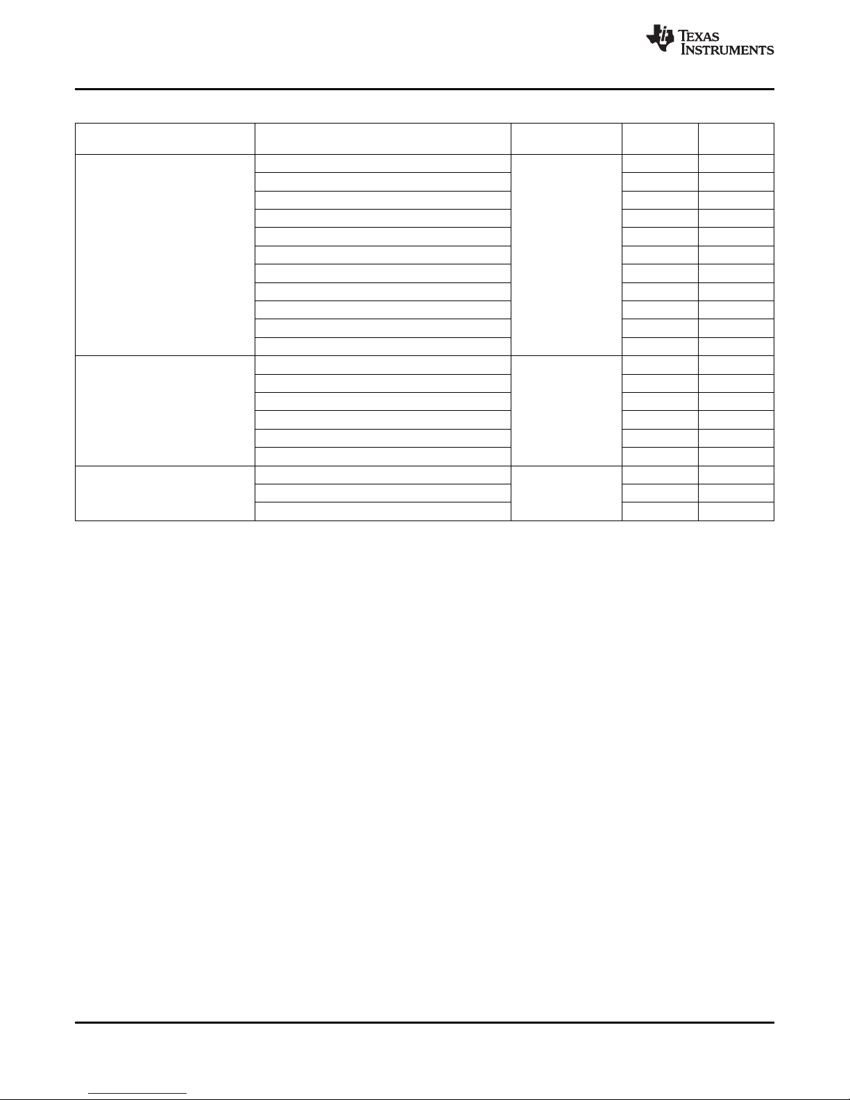
MSP430F5638, MSP430F5637, MSP430F5636
MSP430F5635, MSP430F5634, MSP430F5633
MSP430F5632, MSP430F5631, MSP430F5630
SLAS650D –JUNE 2010–REVISED AUGUST 2013
Table 13. System Module Interrupt Vector Registers (continued)
INTERRUPT VECTOR
REGISTER
SYSSNIV, System NMI VMAIFG 019Ch 0Ah
SYSUNIV, User NMI 019Ah
SYSBERRIV, Bus Error USB wait state timeout 0198h 02h Highest
INTERRUPT EVENT WORD ADDRESS OFFSET PRIORITY
No interrupt pending 00h
SVMLIFG 02h Highest
SVMHIFG 04h
DLYLIFG 06h
DLYHIFG 08h
JMBINIFG 0Ch
JMBOUTIFG 0Eh
SVMLVLRIFG 10h
SVMHVLRIFG 12h
Reserved 14h to 1Eh Lowest
No interrupt pending 00h
NMIFG 02h Highest
OFIFG 04h
ACCVIFG 06h
BUSIFG 08h
Reserved 0Ah to 1Eh Lowest
No interrupt pending 00h
Reserved 04h to 1Eh Lowest
www.ti.com
26 Submit Documentation Feedback Copyright © 2010–2013, Texas Instruments Incorporated
Product Folder Links: MSP430F5638 MSP430F5637 MSP430F5636 MSP430F5635 MSP430F5634 MSP430F5633
MSP430F5632 MSP430F5631 MSP430F5630
Page 27
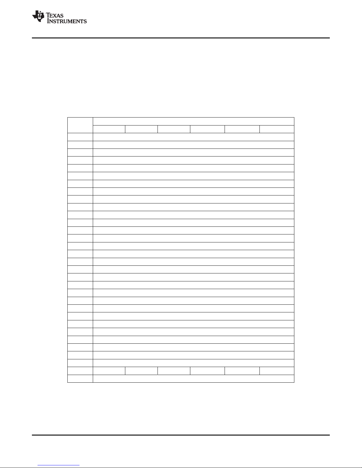
MSP430F5638, MSP430F5637, MSP430F5636
MSP430F5635, MSP430F5634, MSP430F5633
MSP430F5632, MSP430F5631, MSP430F5630
www.ti.com
DMA Controller (Link to User's Guide)
The DMA controller allows movement of data from one memory address to another without CPU intervention. For
example, the DMA controller can be used to move data from the ADC12_A conversion memory to RAM. Using
the DMA controller can increase the throughput of peripheral modules. The DMA controller reduces system
power consumption by allowing the CPU to remain in sleep mode, without having to awaken to move data to or
from a peripheral.
The USB timestamp generator also uses the channel 0, 1, and 2 DMA trigger assignments described in
Table 14.
SLAS650D –JUNE 2010–REVISED AUGUST 2013
Table 14. DMA Trigger Assignments
Trigger
0 DMAREQ
1 TA0CCR0 CCIFG
2 TA0CCR2 CCIFG
3 TA1CCR0 CCIFG
4 TA1CCR2 CCIFG
5 TA2CCR0 CCIFG
6 TA2CCR2 CCIFG
7 TBCCR0 CCIFG
8 TBCCR2 CCIFG
9 Reserved
10 Reserved
11 Reserved
12 Reserved
13 Reserved
14 Reserved
15 Reserved
16 UCA0RXIFG
17 UCA0TXIFG
18 UCB0RXIFG
19 UCB0TXIFG
20 UCA1RXIFG
21 UCA1TXIFG
22 UCB1RXIFG
23 UCB1TXIFG
24 ADC12IFGx
25 DAC12_0IFG
26 DAC12_1IFG
27 USB FNRXD
28 USB ready
29 MPY ready
30 DMA5IFG DMA0IFG DMA1IFG DMA2IFG DMA3IFG DMA4IFG
31 DMAE0
(1) Reserved DMA triggers may be used by other devices in the family. Reserved DMA triggers will not
cause any DMA trigger event when selected.
(2) Only on devices with peripheral module ADC12_A. Reserved on devices without ADC.
(3) Only on devices with peripheral module DAC12_A. Reserved on devices without DAC.
0 1 2 3 4 5
Channel
(2)
(3)
(3)
(1)
Copyright © 2010–2013, Texas Instruments Incorporated Submit Documentation Feedback 27
Product Folder Links: MSP430F5638 MSP430F5637 MSP430F5636 MSP430F5635 MSP430F5634 MSP430F5633
MSP430F5632 MSP430F5631 MSP430F5630
Page 28
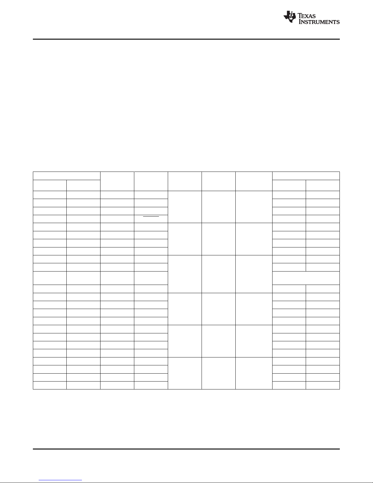
MSP430F5638, MSP430F5637, MSP430F5636
MSP430F5635, MSP430F5634, MSP430F5633
MSP430F5632, MSP430F5631, MSP430F5630
SLAS650D –JUNE 2010–REVISED AUGUST 2013
Universal Serial Communication Interface (USCI) (Links to User's Guide: UART Mode, SPI Mode,
I2C Mode)
The USCI modules are used for serial data communication. The USCI module supports synchronous
communication protocols such as SPI (3 or 4 pin) and I2C, and asynchronous communication protocols such as
UART, enhanced UART with automatic baudrate detection, and IrDA. Each USCI module contains two portions,
A and B.
The USCI_An module provides support for SPI (3 or 4 pin), UART, enhanced UART, or IrDA.
The USCI_Bn module provides support for SPI (3 or 4 pin) or I2C.
The MSP430F563x series includes two complete USCI modules (n = 0 to 1).
Timer TA0 (Link to User's Guide)
Timer TA0 is a 16-bit timer/counter (Timer_A type) with five capture/compare registers. It can support multiple
capture/compares, PWM outputs, and interval timing. It also has extensive interrupt capabilities. Interrupts may
be generated from the counter on overflow conditions and from each of the capture/compare registers.
Table 15. Timer TA0 Signal Connections
INPUT PIN NUMBER DEVICE MODULE MODULE DEVICE OUTPUT PIN NUMBER
PZ ZQW PZ ZQW
34-P1.0 L5-P1.0 TA0CLK TACLK
34-P1.0 L5-P1.0 TA0CLK TACLK
35-P1.1 M5-P1.1 TA0.0 CCI0A 35-P1.1 M5-P1.1
36-P1.2 J6-P1.2 TA0.1 CCI1A 36-P1.2 J6-P1.2
40-P1.6 J7-P1.6 TA0.1 CCI1B 40-P1.6 J7-P1.6
37-P1.3 H6-P1.3 TA0.2 CCI2A 37-P1.3 H6-P1.3
41-P1.7 M7-P1.7 TA0.2 CCI2B 41-P1.7 M7-P1.7
38-P1.4 M6-P1.4 TA0.3 CCI3A 38-P1.4 M6-P1.4
39-P1.5 L6-P1.5 TA0.4 CCI4A 39-P1.5 L6-P1.5
(1) Only on devices with peripheral module ADC12_A.
INPUT INPUT OUTPUT OUTPUT
SIGNAL SIGNAL SIGNAL SIGNAL
ACLK ACLK
SMCLK SMCLK
DV
DV
DV
DV
DV
DV
DV
DV
DV
DV
DV
DV
DV
SS
SS
CC
SS
CC
SS
CC
SS
SS
CC
SS
SS
CC
CCI0B
GND
V
CC
GND
V
CC
GND
V
CC
CCI3B
GND
V
CC
CCI4B
GND
V
CC
MODULE
BLOCK
Timer NA NA
CCR0 TA0 TA0.0
CCR1 TA1 TA0.1
CCR2 TA2 TA0.2
CCR3 TA3 TA0.3
CCR4 TA4 TA0.4
ADC12_A (internal)
ADC12SHSx = {1}
www.ti.com
(1)
28 Submit Documentation Feedback Copyright © 2010–2013, Texas Instruments Incorporated
Product Folder Links: MSP430F5638 MSP430F5637 MSP430F5636 MSP430F5635 MSP430F5634 MSP430F5633
MSP430F5632 MSP430F5631 MSP430F5630
Page 29
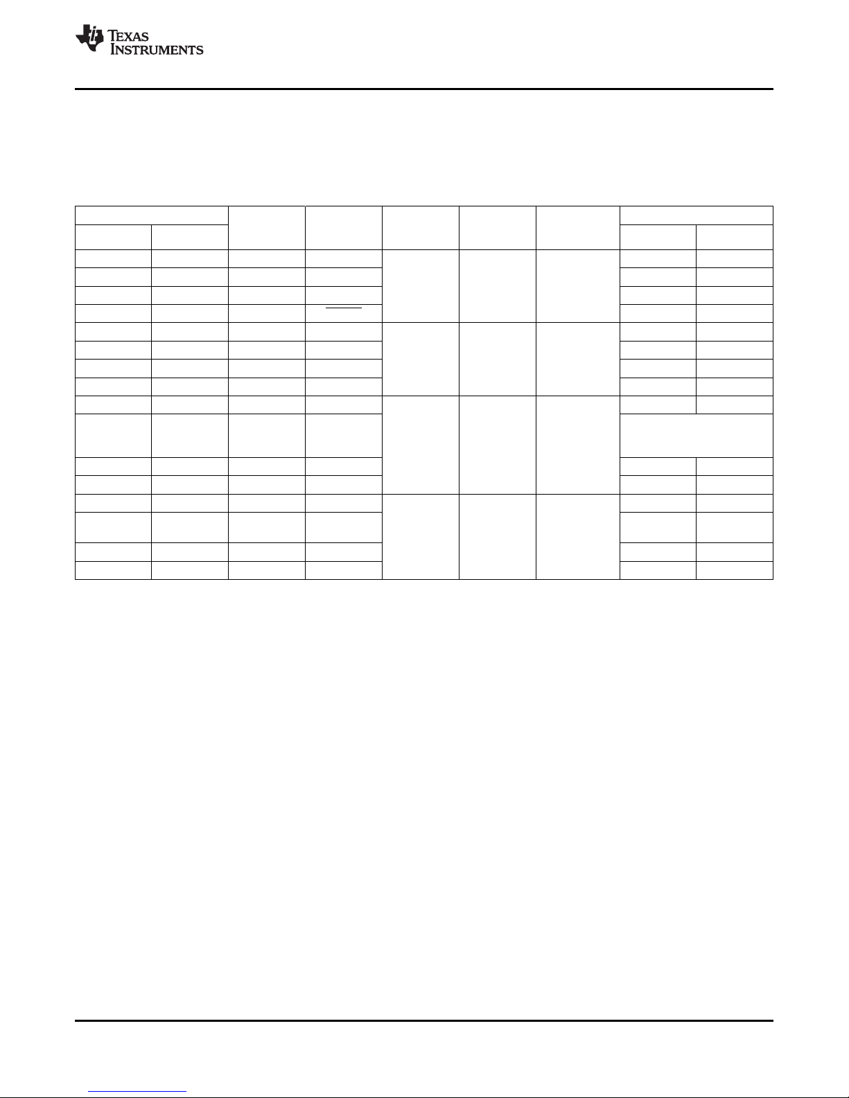
MSP430F5638, MSP430F5637, MSP430F5636
MSP430F5635, MSP430F5634, MSP430F5633
MSP430F5632, MSP430F5631, MSP430F5630
www.ti.com
Timer TA1 (Link to User's Guide)
Timer TA1 is a 16-bit timer/counter (Timer_A type) with three capture/compare registers. It supports multiple
capture/compares, PWM outputs, and interval timing. It also has extensive interrupt capabilities. Interrupts may
be generated from the counter on overflow conditions and from each of the capture/compare registers.
Table 16. Timer TA1 Signal Connections
INPUT PIN NUMBER DEVICE MODULE MODULE DEVICE OUTPUT PIN NUMBER
PZ ZQW PZ ZQW
42-P3.0 L7-P3.0 TA1CLK TACLK
42-P3.0 L7-P3.0 TA1CLK TACLK
43-P3.1 H7-P3.1 TA1.0 CCI0A 43-P3.1 H7-P3.1
44-P3.2 M8-P3.2 TA1.1 CCI1A 44-P3.2 M8-P3.2
45-P3.3 L8-P3.3 TA1.2 CCI2A 45-P3.3 L8-P3.3
(1) Only on devices with peripheral module DAC12_A.
INPUT INPUT OUTPUT OUTPUT
SIGNAL SIGNAL SIGNAL SIGNAL
ACLK ACLK
SMCLK SMCLK
DV
SS
DV
SS
DV
CC
CBOUT
(internal)
DV
SS
DV
CC
ACLK
(internal)
DV
SS
DV
CC
CCI0B
GND
V
CC
CCI1B DAC12_0, DAC12_1
GND
V
CC
CCI2B
GND
V
CC
MODULE
BLOCK
Timer NA NA
CCR0 TA0 TA1.0
CCR1 TA1 TA1.1
CCR2 TA2 TA1.2
SLAS650D –JUNE 2010–REVISED AUGUST 2013
DAC12_A
(internal)
(1)
Copyright © 2010–2013, Texas Instruments Incorporated Submit Documentation Feedback 29
Product Folder Links: MSP430F5638 MSP430F5637 MSP430F5636 MSP430F5635 MSP430F5634 MSP430F5633
MSP430F5632 MSP430F5631 MSP430F5630
Page 30
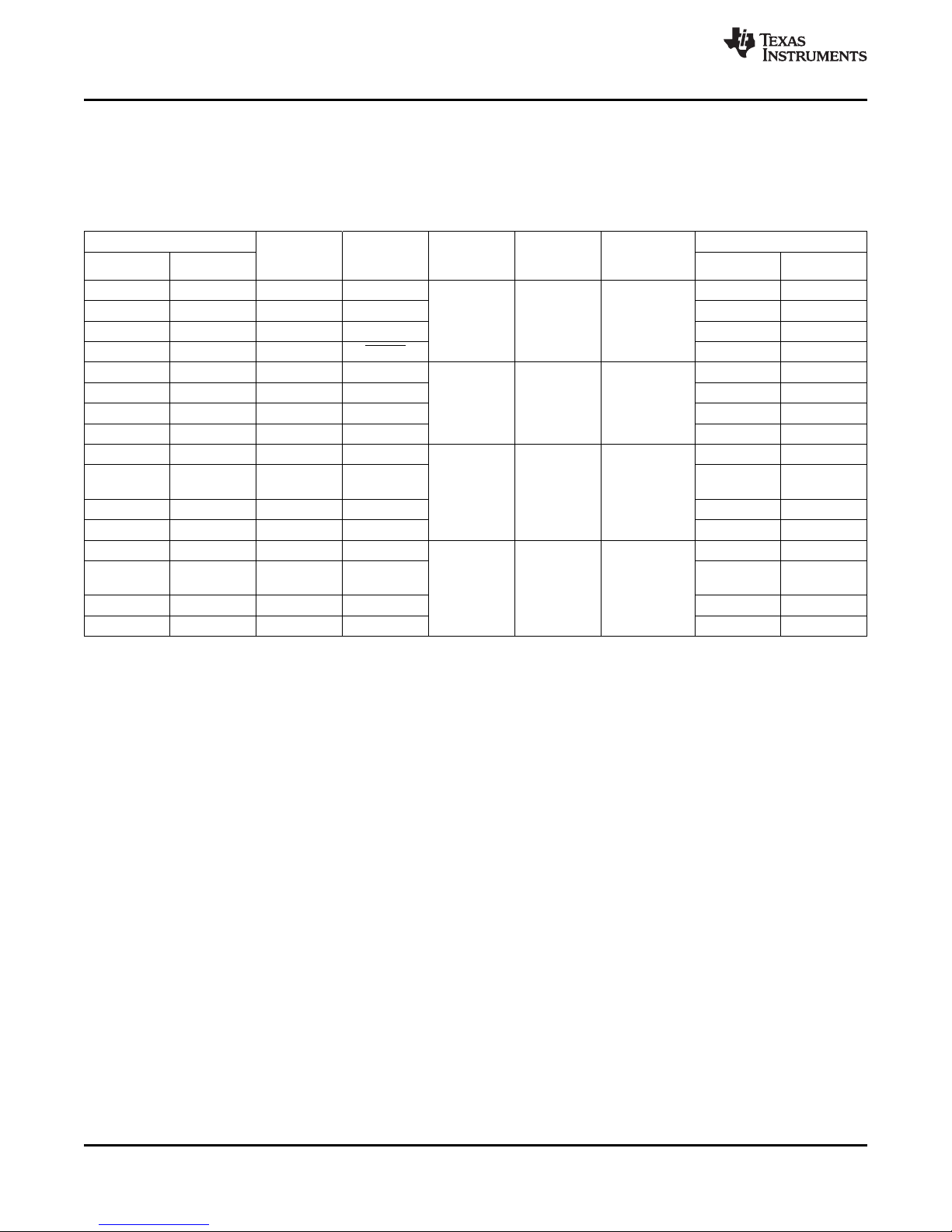
MSP430F5638, MSP430F5637, MSP430F5636
MSP430F5635, MSP430F5634, MSP430F5633
MSP430F5632, MSP430F5631, MSP430F5630
SLAS650D –JUNE 2010–REVISED AUGUST 2013
Timer TA2 (Link to User's Guide)
Timer TA2 is a 16-bit timer/counter (Timer_A type) with three capture/compare registers. It supports multiple
capture/compares, PWM outputs, and interval timing. It also has extensive interrupt capabilities. Interrupts may
be generated from the counter on overflow conditions and from each of the capture/compare registers.
Table 17. Timer TA2 Signal Connections
INPUT PIN NUMBER DEVICE MODULE MODULE DEVICE OUTPUT PIN NUMBER
PZ ZQW PZ ZQW
46-P3.4 J8-P3.4 TA2CLK TACLK
46-P3.4 J8-P3.4 TA2CLK TACLK
47-P3.5 M9-P3.5 TA2.0 CCI0A 47-P3.5 M9-P3.5
48-P3.6 L9-P3.6 TA2.1 CCI1A 48-P3.6 L9-P3.6
49-P3.7 M10-P3.7 TA2.2 CCI2A 49-P3.7 M10-P3.7
INPUT INPUT OUTPUT OUTPUT
SIGNAL SIGNAL SIGNAL SIGNAL
ACLK ACLK
SMCLK SMCLK
DV
SS
DV
SS
DV
CC
CBOUT
(internal)
DV
SS
DV
CC
ACLK
(internal)
DV
SS
DV
CC
CCI0B
GND
V
CC
CCI1B
GND
V
CC
CCI2B
GND
V
CC
MODULE
BLOCK
Timer NA NA
CCR0 TA0 TA2.0
CCR1 TA1 TA2.1
CCR2 TA2 TA2.2
www.ti.com
30 Submit Documentation Feedback Copyright © 2010–2013, Texas Instruments Incorporated
Product Folder Links: MSP430F5638 MSP430F5637 MSP430F5636 MSP430F5635 MSP430F5634 MSP430F5633
MSP430F5632 MSP430F5631 MSP430F5630
Page 31

MSP430F5638, MSP430F5637, MSP430F5636
MSP430F5635, MSP430F5634, MSP430F5633
MSP430F5632, MSP430F5631, MSP430F5630
www.ti.com
Timer TB0 (Link to User's Guide)
Timer TB0 is a 16-bit timer/counter (Timer_B type) with seven capture/compare registers. It supports multiple
capture/compares, PWM outputs, and interval timing. It also has extensive interrupt capabilities. Interrupts may
be generated from the counter on overflow conditions and from each of the capture/compare registers.
Table 18. Timer TB0 Signal Connections
INPUT PIN NUMBER DEVICE MODULE MODULE DEVICE OUTPUT PIN NUMBER
PZ ZQW PZ ZQW
58-P8.0 J11-P8.0
P2MAPx
(1)
P2MAPx
(1)
INPUT INPUT OUTPUT OUTPUT
SIGNAL SIGNAL SIGNAL SIGNAL
TB0CLK TB0CLK
ACLK ACLK
SMCLK SMCLK
58-P8.0 J11-P8.0
P2MAPx
(1)
P2MAPx
TB0CLK TB0CLK
(1)
50-P4.0 J9-P4.0 TB0.0 CCI0A 50-P4.0 J9-P4.0
P2MAPx
(1)
P2MAPx
(1)
TB0.0 CCI0B P2MAPx
DV
DV
SS
CC
GND
V
CC
51-P4.1 M11-P4.1 TB0.1 CCI1A 51-P4.1 M11-P4.1
P2MAPx
(1)
P2MAPx
(1)
TB0.1 CCI1B P2MAPx
DV
DV
SS
CC
GND
V
CC
52-P4.2 L10-P4.2 TB0.2 CCI2A 52-P4.2 L10-P4.2
P2MAPx
(1)
P2MAPx
(1)
TB0.2 CCI2B P2MAPx
DV
DV
SS
CC
GND DAC12_0, DAC12_1
V
CC
53-P4.3 M12-P4.3 TB0.3 CCI3A 53-P4.3 M12-P4.3
P2MAPx
(1)
P2MAPx
(1)
TB0.3 CCI3B P2MAPx
DV
DV
SS
CC
GND
V
CC
54-P4.4 L12-P4.4 TB0.4 CCI4A 54-P4.4 L12-P4.4
P2MAPx
(1)
P2MAPx
(1)
TB0.4 CCI4B P2MAPx
DV
DV
SS
CC
GND
V
CC
55-P4.5 L11-P4.5 TB0.5 CCI5A 55-P4.5 L11-P4.5
P2MAPx
(1)
P2MAPx
(1)
TB0.5 CCI5B P2MAPx
DV
DV
SS
CC
GND
V
CC
56-P4.6 K11-P4.6 TB0.6 CCI6A 56-P4.6 K11-P4.6
P2MAPx
(1)
P2MAPx
(1)
TB0.6 CCI6B P2MAPx
DV
DV
SS
CC
GND
V
CC
(1) Timer functions selectable via the port mapping controller.
(2) Only on devices with peripheral module ADC12_A.
(3) Only on devices with peripheral module DAC12_A.
MODULE
BLOCK
Timer NA NA
CCR0 TB0 TB0.0
CCR1 TB1 TB0.1
CCR2 TB2 TB0.2
CCR3 TB3 TB0.3
CCR4 TB4 TB0.4
CCR5 TB5 TB0.5
CCR6 TB6 TB0.6
SLAS650D –JUNE 2010–REVISED AUGUST 2013
(1)
P2MAPx
ADC12 (internal)
(1)
(2)
ADC12SHSx = {2}
(1)
P2MAPx
ADC12 (internal)
(1)
(2)
ADC12SHSx = {3}
(1)
DAC12_A
P2MAPx
(1)
(3)
(internal)
(1)
P2MAPx
(1)
P2MAPx
(1)
P2MAPx
(1)
P2MAPx
(1)
(1)
(1)
(1)
Copyright © 2010–2013, Texas Instruments Incorporated Submit Documentation Feedback 31
Product Folder Links: MSP430F5638 MSP430F5637 MSP430F5636 MSP430F5635 MSP430F5634 MSP430F5633
MSP430F5632 MSP430F5631 MSP430F5630
Page 32

MSP430F5638, MSP430F5637, MSP430F5636
MSP430F5635, MSP430F5634, MSP430F5633
MSP430F5632, MSP430F5631, MSP430F5630
SLAS650D –JUNE 2010–REVISED AUGUST 2013
Comparator_B (Link to User's Guide)
The primary function of the Comparator_B module is to support precision slope analog-to-digital conversions,
battery voltage supervision, and monitoring of external analog signals.
ADC12_A (Link to User's Guide)
The ADC12_A module supports fast 12-bit analog-to-digital conversions. The module implements a 12-bit SAR
core, sample select control, reference generator, and a 16-word conversion-and-control buffer. The conversionand-control buffer allows up to 16 independent ADC samples to be converted and stored without any CPU
intervention.
DAC12_A (Link to User's Guide)
The DAC12_A module is a 12-bit R-ladder voltage-output DAC. The DAC12_A may be used in 8-bit or 12-bit
mode, and may be used in conjunction with the DMA controller. When multiple DAC12_A modules are present,
they may be grouped together for synchronous operation.
CRC16 (Link to User's Guide)
The CRC16 module produces a signature based on a sequence of entered data values and can be used for data
checking purposes. The CRC16 module signature is based on the CRC-CCITT standard.
www.ti.com
REF Voltage Reference (Link to User's Guide)
The reference module (REF) is responsible for generation of all critical reference voltages that can be used by
the various analog peripherals in the device.
USB Universal Serial Bus (Link to User's Guide)
The USB module is a fully integrated USB interface that is compliant with the USB 2.0 specification. The module
supports full-speed operation of control, interrupt, and bulk transfers. The module includes an integrated LDO,
PHY, and PLL. The PLL is highly flexible and can support a wide range of input clock frequencies. USB RAM,
when not used for USB communication, can be used by the system.
Embedded Emulation Module (EEM) (Link to User's Guide)
The Embedded Emulation Module (EEM) supports real-time in-system debugging. The L version of the EEM
implemented on these devices has the following features:
• Eight hardware triggers or breakpoints on memory access
• Two hardware triggers or breakpoints on CPU register write access
• Up to ten hardware triggers can be combined to form complex triggers or breakpoints
• Two cycle counters
• Sequencer
• State storage
• Clock control on module level
32 Submit Documentation Feedback Copyright © 2010–2013, Texas Instruments Incorporated
Product Folder Links: MSP430F5638 MSP430F5637 MSP430F5636 MSP430F5635 MSP430F5634 MSP430F5633
MSP430F5632 MSP430F5631 MSP430F5630
Page 33

MSP430F5638, MSP430F5637, MSP430F5636
MSP430F5635, MSP430F5634, MSP430F5633
MSP430F5632, MSP430F5631, MSP430F5630
www.ti.com
Peripheral File Map
Table 19. Peripherals
MODULE NAME BASE ADDRESS OFFSET ADDRESS RANGE
Special Functions (see Table 20) 0100h 000h-01Fh
PMM (see Table 21) 0120h 000h-010h
Flash Control (see Table 22) 0140h 000h-00Fh
CRC16 (see Table 23) 0150h 000h-007h
RAM Control (see Table 24) 0158h 000h-001h
Watchdog (see Table 25) 015Ch 000h-001h
UCS (see Table 26) 0160h 000h-01Fh
SYS (see Table 27) 0180h 000h-01Fh
Shared Reference (see Table 28) 01B0h 000h-001h
Port Mapping Control (see Table 29) 01C0h 000h-003h
Port Mapping Port P2 (see Table 29) 01D0h 000h-007h
Port P1/P2 (see Table 30) 0200h 000h-01Fh
Port P3/P4 (see Table 31) 0220h 000h-01Fh
Port P5/P6 (see Table 32) 0240h 000h-00Bh
Port P7/P8 (see Table 33) 0260h 000h-00Bh
Port P9 (see Table 34) 0280h 000h-00Bh
Port PJ (see Table 35) 0320h 000h-01Fh
Timer TA0 (see Table 36) 0340h 000h-02Eh
Timer TA1 (see Table 37) 0380h 000h-02Eh
Timer TB0 (see Table 38) 03C0h 000h-02Eh
Timer TA2 (see Table 39) 0400h 000h-02Eh
Battery Backup (see Table 40) 0480h 000h-01Fh
RTC_B (see Table 41) 04A0h 000h-01Fh
32-bit Hardware Multiplier (see Table 42) 04C0h 000h-02Fh
DMA General Control (see Table 43) 0500h 000h-00Fh
DMA Channel 0 (see Table 43) 0510h 000h-00Ah
DMA Channel 1 (see Table 43) 0520h 000h-00Ah
DMA Channel 2 (see Table 43) 0530h 000h-00Ah
DMA Channel 3 (see Table 43) 0540h 000h-00Ah
DMA Channel 4 (see Table 43) 0550h 000h-00Ah
DMA Channel 5 (see Table 43) 0560h 000h-00Ah
USCI_A0 (see Table 44) 05C0h 000h-01Fh
USCI_B0 (see Table 45) 05E0h 000h-01Fh
USCI_A1 (see Table 46) 0600h 000h-01Fh
USCI_B1 (see Table 47) 0620h 000h-01Fh
ADC12_A (see Table 48) 0700h 000h-03Fh
DAC12_A (see Table 49) 0780h 000h-01Fh
Comparator_B (see Table 50) 08C0h 000h-00Fh
USB configuration (see Table 51) 0900h 000h-014h
USB control (see Table 52) 0920h 000h-01Fh
(1) For a detailed description of the individual control register offset addresses, see the MSP430x5xx and MSP430x6xx Family User's Guide
(SLAU208).
SLAS650D –JUNE 2010–REVISED AUGUST 2013
(1)
Copyright © 2010–2013, Texas Instruments Incorporated Submit Documentation Feedback 33
Product Folder Links: MSP430F5638 MSP430F5637 MSP430F5636 MSP430F5635 MSP430F5634 MSP430F5633
MSP430F5632 MSP430F5631 MSP430F5630
Page 34

MSP430F5638, MSP430F5637, MSP430F5636
MSP430F5635, MSP430F5634, MSP430F5633
MSP430F5632, MSP430F5631, MSP430F5630
SLAS650D –JUNE 2010–REVISED AUGUST 2013
Table 20. Special Function Registers (Base Address: 0100h)
REGISTER DESCRIPTION REGISTER OFFSET
SFR interrupt enable SFRIE1 00h
SFR interrupt flag SFRIFG1 02h
SFR reset pin control SFRRPCR 04h
Table 21. PMM Registers (Base Address: 0120h)
REGISTER DESCRIPTION REGISTER OFFSET
PMM Control 0 PMMCTL0 00h
PMM control 1 PMMCTL1 02h
SVS high side control SVSMHCTL 04h
SVS low side control SVSMLCTL 06h
PMM interrupt flags PMMIFG 0Ch
PMM interrupt enable PMMIE 0Eh
PMM power mode 5 control PM5CTL0 10h
Table 22. Flash Control Registers (Base Address: 0140h)
REGISTER DESCRIPTION REGISTER OFFSET
Flash control 1 FCTL1 00h
Flash control 3 FCTL3 04h
Flash control 4 FCTL4 06h
www.ti.com
Table 23. CRC16 Registers (Base Address: 0150h)
REGISTER DESCRIPTION REGISTER OFFSET
CRC data input CRC16DI 00h
CRC result CRC16INIRES 04h
Table 24. RAM Control Registers (Base Address: 0158h)
REGISTER DESCRIPTION REGISTER OFFSET
RAM control 0 RCCTL0 00h
Table 25. Watchdog Registers (Base Address: 015Ch)
REGISTER DESCRIPTION REGISTER OFFSET
Watchdog timer control WDTCTL 00h
Table 26. UCS Registers (Base Address: 0160h)
REGISTER DESCRIPTION REGISTER OFFSET
UCS control 0 UCSCTL0 00h
UCS control 1 UCSCTL1 02h
UCS control 2 UCSCTL2 04h
UCS control 3 UCSCTL3 06h
UCS control 4 UCSCTL4 08h
UCS control 5 UCSCTL5 0Ah
UCS control 6 UCSCTL6 0Ch
UCS control 7 UCSCTL7 0Eh
UCS control 8 UCSCTL8 10h
34 Submit Documentation Feedback Copyright © 2010–2013, Texas Instruments Incorporated
Product Folder Links: MSP430F5638 MSP430F5637 MSP430F5636 MSP430F5635 MSP430F5634 MSP430F5633
MSP430F5632 MSP430F5631 MSP430F5630
Page 35

MSP430F5638, MSP430F5637, MSP430F5636
MSP430F5635, MSP430F5634, MSP430F5633
MSP430F5632, MSP430F5631, MSP430F5630
www.ti.com
Table 27. SYS Registers (Base Address: 0180h)
REGISTER DESCRIPTION REGISTER OFFSET
System control SYSCTL 00h
Bootstrap loader configuration area SYSBSLC 02h
JTAG mailbox control SYSJMBC 06h
JTAG mailbox input 0 SYSJMBI0 08h
JTAG mailbox input 1 SYSJMBI1 0Ah
JTAG mailbox output 0 SYSJMBO0 0Ch
JTAG mailbox output 1 SYSJMBO1 0Eh
Bus Error vector generator SYSBERRIV 18h
User NMI vector generator SYSUNIV 1Ah
System NMI vector generator SYSSNIV 1Ch
Reset vector generator SYSRSTIV 1Eh
Table 28. Shared Reference Registers (Base Address: 01B0h)
REGISTER DESCRIPTION REGISTER OFFSET
Shared reference control REFCTL 00h
SLAS650D –JUNE 2010–REVISED AUGUST 2013
Table 29. Port Mapping Registers
(Base Address of Port Mapping Control: 01C0h, Port P2: 01D0h)
REGISTER DESCRIPTION REGISTER OFFSET
Port mapping password register PMAPPWD 00h
Port mapping control register PMAPCTL 02h
Port P2.0 mapping register P2MAP0 00h
Port P2.1 mapping register P2MAP1 01h
Port P2.2 mapping register P2MAP2 02h
Port P2.3 mapping register P2MAP3 03h
Port P2.4 mapping register P2MAP4 04h
Port P2.5 mapping register P2MAP5 05h
Port P2.6 mapping register P2MAP6 06h
Port P2.7 mapping register P2MAP7 07h
Table 30. Port P1/P2 Registers (Base Address: 0200h)
REGISTER DESCRIPTION REGISTER OFFSET
Port P1 input P1IN 00h
Port P1 output P1OUT 02h
Port P1 direction P1DIR 04h
Port P1 pullup/pulldown enable P1REN 06h
Port P1 drive strength P1DS 08h
Port P1 selection P1SEL 0Ah
Port P1 interrupt vector word P1IV 0Eh
Port P1 interrupt edge select P1IES 18h
Port P1 interrupt enable P1IE 1Ah
Port P1 interrupt flag P1IFG 1Ch
Port P2 input P2IN 01h
Port P2 output P2OUT 03h
Port P2 direction P2DIR 05h
Port P2 pullup/pulldown enable P2REN 07h
Port P2 drive strength P2DS 09h
Copyright © 2010–2013, Texas Instruments Incorporated Submit Documentation Feedback 35
Product Folder Links: MSP430F5638 MSP430F5637 MSP430F5636 MSP430F5635 MSP430F5634 MSP430F5633
MSP430F5632 MSP430F5631 MSP430F5630
Page 36

MSP430F5638, MSP430F5637, MSP430F5636
MSP430F5635, MSP430F5634, MSP430F5633
MSP430F5632, MSP430F5631, MSP430F5630
SLAS650D –JUNE 2010–REVISED AUGUST 2013
Table 30. Port P1/P2 Registers (Base Address: 0200h) (continued)
REGISTER DESCRIPTION REGISTER OFFSET
Port P2 selection P2SEL 0Bh
Port P2 interrupt vector word P2IV 1Eh
Port P2 interrupt edge select P2IES 19h
Port P2 interrupt enable P2IE 1Bh
Port P2 interrupt flag P2IFG 1Dh
Table 31. Port P3/P4 Registers (Base Address: 0220h)
REGISTER DESCRIPTION REGISTER OFFSET
Port P3 input P3IN 00h
Port P3 output P3OUT 02h
Port P3 direction P3DIR 04h
Port P3 pullup/pulldown enable P3REN 06h
Port P3 drive strength P3DS 08h
Port P3 selection P3SEL 0Ah
Port P3 interrupt vector word P3IV 0Eh
Port P3 interrupt edge select P3IES 18h
Port P3 interrupt enable P3IE 1Ah
Port P3 interrupt flag P3IFG 1Ch
Port P4 input P4IN 01h
Port P4 output P4OUT 03h
Port P4 direction P4DIR 05h
Port P4 pullup/pulldown enable P4REN 07h
Port P4 drive strength P4DS 09h
Port P4 selection P4SEL 0Bh
Port P4 interrupt vector word P4IV 1Eh
Port P4 interrupt edge select P4IES 19h
Port P4 interrupt enable P4IE 1Bh
Port P4 interrupt flag P4IFG 1Dh
www.ti.com
Table 32. Port P5/P6 Registers (Base Address: 0240h)
REGISTER DESCRIPTION REGISTER OFFSET
Port P5 input P5IN 00h
Port P5 output P5OUT 02h
Port P5 direction P5DIR 04h
Port P5 pullup/pulldown enable P5REN 06h
Port P5 drive strength P5DS 08h
Port P5 selection P5SEL 0Ah
Port P6 input P6IN 01h
Port P6 output P6OUT 03h
Port P6 direction P6DIR 05h
Port P6 pullup/pulldown enable P6REN 07h
Port P6 drive strength P6DS 09h
Port P6 selection P6SEL 0Bh
36 Submit Documentation Feedback Copyright © 2010–2013, Texas Instruments Incorporated
Product Folder Links: MSP430F5638 MSP430F5637 MSP430F5636 MSP430F5635 MSP430F5634 MSP430F5633
MSP430F5632 MSP430F5631 MSP430F5630
Page 37

MSP430F5638, MSP430F5637, MSP430F5636
MSP430F5635, MSP430F5634, MSP430F5633
MSP430F5632, MSP430F5631, MSP430F5630
www.ti.com
Table 33. Port P7/P8 Registers (Base Address: 0260h)
REGISTER DESCRIPTION REGISTER OFFSET
Port P7 input P7IN 00h
Port P7 output P7OUT 02h
Port P7 direction P7DIR 04h
Port P7 pullup/pulldown enable P7REN 06h
Port P7 drive strength P7DS 08h
Port P7 selection P7SEL 0Ah
Port P8 input P8IN 01h
Port P8 output P8OUT 03h
Port P8 direction P8DIR 05h
Port P8 pullup/pulldown enable P8REN 07h
Port P8 drive strength P8DS 09h
Port P8 selection P8SEL 0Bh
Table 34. Port P9 Register (Base Address: 0280h)
REGISTER DESCRIPTION REGISTER OFFSET
Port P9 input P9IN 00h
Port P9 output P9OUT 02h
Port P9 direction P9DIR 04h
Port P9 pullup/pulldown enable P9REN 06h
Port P9 drive strength P9DS 08h
Port P9 selection P9SEL 0Ah
SLAS650D –JUNE 2010–REVISED AUGUST 2013
Table 35. Port J Registers (Base Address: 0320h)
REGISTER DESCRIPTION REGISTER OFFSET
Port PJ input PJIN 00h
Port PJ output PJOUT 02h
Port PJ direction PJDIR 04h
Port PJ pullup/pulldown enable PJREN 06h
Port PJ drive strength PJDS 08h
Table 36. TA0 Registers (Base Address: 0340h)
REGISTER DESCRIPTION REGISTER OFFSET
TA0 control TA0CTL 00h
Capture/compare control 0 TA0CCTL0 02h
Capture/compare control 1 TA0CCTL1 04h
Capture/compare control 2 TA0CCTL2 06h
Capture/compare control 3 TA0CCTL3 08h
Capture/compare control 4 TA0CCTL4 0Ah
TA0 counter register TA0R 10h
Capture/compare register 0 TA0CCR0 12h
Capture/compare register 1 TA0CCR1 14h
Capture/compare register 2 TA0CCR2 16h
Capture/compare register 3 TA0CCR3 18h
Capture/compare register 4 TA0CCR4 1Ah
TA0 expansion register 0 TA0EX0 20h
TA0 interrupt vector TA0IV 2Eh
Copyright © 2010–2013, Texas Instruments Incorporated Submit Documentation Feedback 37
Product Folder Links: MSP430F5638 MSP430F5637 MSP430F5636 MSP430F5635 MSP430F5634 MSP430F5633
MSP430F5632 MSP430F5631 MSP430F5630
Page 38

MSP430F5638, MSP430F5637, MSP430F5636
MSP430F5635, MSP430F5634, MSP430F5633
MSP430F5632, MSP430F5631, MSP430F5630
SLAS650D –JUNE 2010–REVISED AUGUST 2013
Table 37. TA1 Registers (Base Address: 0380h)
REGISTER DESCRIPTION REGISTER OFFSET
TA1 control TA1CTL 00h
Capture/compare control 0 TA1CCTL0 02h
Capture/compare control 1 TA1CCTL1 04h
Capture/compare control 2 TA1CCTL2 06h
TA1 counter register TA1R 10h
Capture/compare register 0 TA1CCR0 12h
Capture/compare register 1 TA1CCR1 14h
Capture/compare register 2 TA1CCR2 16h
TA1 expansion register 0 TA1EX0 20h
TA1 interrupt vector TA1IV 2Eh
Table 38. TB0 Registers (Base Address: 03C0h)
REGISTER DESCRIPTION REGISTER OFFSET
TB0 control TB0CTL 00h
Capture/compare control 0 TB0CCTL0 02h
Capture/compare control 1 TB0CCTL1 04h
Capture/compare control 2 TB0CCTL2 06h
Capture/compare control 3 TB0CCTL3 08h
Capture/compare control 4 TB0CCTL4 0Ah
Capture/compare control 5 TB0CCTL5 0Ch
Capture/compare control 6 TB0CCTL6 0Eh
TB0 register TB0R 10h
Capture/compare register 0 TB0CCR0 12h
Capture/compare register 1 TB0CCR1 14h
Capture/compare register 2 TB0CCR2 16h
Capture/compare register 3 TB0CCR3 18h
Capture/compare register 4 TB0CCR4 1Ah
Capture/compare register 5 TB0CCR5 1Ch
Capture/compare register 6 TB0CCR6 1Eh
TB0 expansion register 0 TB0EX0 20h
TB0 interrupt vector TB0IV 2Eh
www.ti.com
Table 39. TA2 Registers (Base Address: 0400h)
REGISTER DESCRIPTION REGISTER OFFSET
TA2 control TA2CTL 00h
Capture/compare control 0 TA2CCTL0 02h
Capture/compare control 1 TA2CCTL1 04h
Capture/compare control 2 TA2CCTL2 06h
TA2 counter register TA2R 10h
Capture/compare register 0 TA2CCR0 12h
Capture/compare register 1 TA2CCR1 14h
Capture/compare register 2 TA2CCR2 16h
TA2 expansion register 0 TA2EX0 20h
TA2 interrupt vector TA2IV 2Eh
38 Submit Documentation Feedback Copyright © 2010–2013, Texas Instruments Incorporated
Product Folder Links: MSP430F5638 MSP430F5637 MSP430F5636 MSP430F5635 MSP430F5634 MSP430F5633
MSP430F5632 MSP430F5631 MSP430F5630
Page 39

MSP430F5638, MSP430F5637, MSP430F5636
MSP430F5635, MSP430F5634, MSP430F5633
MSP430F5632, MSP430F5631, MSP430F5630
www.ti.com
Table 40. Battery Backup Registers (Base Address: 0480h)
REGISTER DESCRIPTION REGISTER OFFSET
Battery Backup Memory 0 BAKMEM0 00h
Battery Backup Memory 1 BAKMEM1 02h
Battery Backup Memory 2 BAKMEM2 04h
Battery Backup Memory 3 BAKMEM3 06h
Battery Backup Control BAKCTL 1Ch
Battery Charger Control BAKCHCTL 1Eh
Table 41. Real-Time Clock Registers (Base Address: 04A0h)
REGISTER DESCRIPTION REGISTER OFFSET
RTC control register 0 RTCCTL0 00h
RTC control register 1 RTCCTL1 01h
RTC control register 2 RTCCTL2 02h
RTC control register 3 RTCCTL3 03h
RTC prescaler 0 control register RTCPS0CTL 08h
RTC prescaler 1 control register RTCPS1CTL 0Ah
RTC prescaler 0 RTCPS0 0Ch
RTC prescaler 1 RTCPS1 0Dh
RTC interrupt vector word RTCIV 0Eh
RTC seconds RTCSEC 10h
RTC minutes RTCMIN 11h
RTC hours RTCHOUR 12h
RTC day of week RTCDOW 13h
RTC days RTCDAY 14h
RTC month RTCMON 15h
RTC year low RTCYEARL 16h
RTC year high RTCYEARH 17h
RTC alarm minutes RTCAMIN 18h
RTC alarm hours RTCAHOUR 19h
RTC alarm day of week RTCADOW 1Ah
RTC alarm days RTCADAY 1Bh
Binary-to-BCD conversion register BIN2BCD 1Ch
BCD-to-binary conversion register BCD2BIN 1Eh
SLAS650D –JUNE 2010–REVISED AUGUST 2013
Table 42. 32-bit Hardware Multiplier Registers (Base Address: 04C0h)
REGISTER DESCRIPTION REGISTER OFFSET
16-bit operand 1 – multiply MPY 00h
16-bit operand 1 – signed multiply MPYS 02h
16-bit operand 1 – multiply accumulate MAC 04h
16-bit operand 1 – signed multiply accumulate MACS 06h
16-bit operand 2 OP2 08h
16 × 16 result low word RESLO 0Ah
16 × 16 result high word RESHI 0Ch
16 × 16 sum extension register SUMEXT 0Eh
32-bit operand 1 – multiply low word MPY32L 10h
32-bit operand 1 – multiply high word MPY32H 12h
32-bit operand 1 – signed multiply low word MPYS32L 14h
32-bit operand 1 – signed multiply high word MPYS32H 16h
Copyright © 2010–2013, Texas Instruments Incorporated Submit Documentation Feedback 39
Product Folder Links: MSP430F5638 MSP430F5637 MSP430F5636 MSP430F5635 MSP430F5634 MSP430F5633
MSP430F5632 MSP430F5631 MSP430F5630
Page 40

MSP430F5638, MSP430F5637, MSP430F5636
MSP430F5635, MSP430F5634, MSP430F5633
MSP430F5632, MSP430F5631, MSP430F5630
SLAS650D –JUNE 2010–REVISED AUGUST 2013
Table 42. 32-bit Hardware Multiplier Registers (Base Address: 04C0h) (continued)
REGISTER DESCRIPTION REGISTER OFFSET
32-bit operand 1 – multiply accumulate low word MAC32L 18h
32-bit operand 1 – multiply accumulate high word MAC32H 1Ah
32-bit operand 1 – signed multiply accumulate low word MACS32L 1Ch
32-bit operand 1 – signed multiply accumulate high word MACS32H 1Eh
32-bit operand 2 – low word OP2L 20h
32-bit operand 2 – high word OP2H 22h
32 × 32 result 0 – least significant word RES0 24h
32 × 32 result 1 RES1 26h
32 × 32 result 2 RES2 28h
32 × 32 result 3 – most significant word RES3 2Ah
MPY32 control register 0 MPY32CTL0 2Ch
Table 43. DMA Registers (Base Address DMA General Control: 0500h,
DMA Channel 0: 0510h, DMA Channel 1: 0520h, DMA Channel 2: 0530h, DMA Channel 3: 0540h, DMA
Channel 4: 0550h, DMA Channel 5: 0560h)
REGISTER DESCRIPTION REGISTER OFFSET
DMA General Control: DMA module control 0 DMACTL0 00h
DMA General Control: DMA module control 1 DMACTL1 02h
DMA General Control: DMA module control 2 DMACTL2 04h
DMA General Control: DMA module control 3 DMACTL3 06h
DMA General Control: DMA module control 4 DMACTL4 08h
DMA General Control: DMA interrupt vector DMAIV 0Ah
DMA Channel 0 control DMA0CTL 00h
DMA Channel 0 source address low DMA0SAL 02h
DMA Channel 0 source address high DMA0SAH 04h
DMA Channel 0 destination address low DMA0DAL 06h
DMA Channel 0 destination address high DMA0DAH 08h
DMA Channel 0 transfer size DMA0SZ 0Ah
DMA Channel 1 control DMA1CTL 00h
DMA Channel 1 source address low DMA1SAL 02h
DMA Channel 1 source address high DMA1SAH 04h
DMA Channel 1 destination address low DMA1DAL 06h
DMA Channel 1 destination address high DMA1DAH 08h
DMA Channel 1 transfer size DMA1SZ 0Ah
DMA Channel 2 control DMA2CTL 00h
DMA Channel 2 source address low DMA2SAL 02h
DMA Channel 2 source address high DMA2SAH 04h
DMA Channel 2 destination address low DMA2DAL 06h
DMA Channel 2 destination address high DMA2DAH 08h
DMA Channel 2 transfer size DMA2SZ 0Ah
DMA Channel 3 control DMA3CTL 00h
DMA Channel 3 source address low DMA3SAL 02h
DMA Channel 3 source address high DMA3SAH 04h
DMA Channel 3 destination address low DMA3DAL 06h
DMA Channel 3 destination address high DMA3DAH 08h
DMA Channel 3 transfer size DMA3SZ 0Ah
DMA Channel 4 control DMA4CTL 00h
DMA Channel 4 source address low DMA4SAL 02h
www.ti.com
40 Submit Documentation Feedback Copyright © 2010–2013, Texas Instruments Incorporated
Product Folder Links: MSP430F5638 MSP430F5637 MSP430F5636 MSP430F5635 MSP430F5634 MSP430F5633
MSP430F5632 MSP430F5631 MSP430F5630
Page 41

MSP430F5638, MSP430F5637, MSP430F5636
MSP430F5635, MSP430F5634, MSP430F5633
MSP430F5632, MSP430F5631, MSP430F5630
www.ti.com
Table 43. DMA Registers (Base Address DMA General Control: 0500h,
DMA Channel 0: 0510h, DMA Channel 1: 0520h, DMA Channel 2: 0530h, DMA Channel 3: 0540h, DMA
Channel 4: 0550h, DMA Channel 5: 0560h) (continued)
REGISTER DESCRIPTION REGISTER OFFSET
DMA Channel 4 source address high DMA4SAH 04h
DMA Channel 4 destination address low DMA4DAL 06h
DMA Channel 4 destination address high DMA4DAH 08h
DMA Channel 4 transfer size DMA4SZ 0Ah
DMA Channel 5 control DMA5CTL 00h
DMA Channel 5 source address low DMA5SAL 02h
DMA Channel 5 source address high DMA5SAH 04h
DMA Channel 5 destination address low DMA5DAL 06h
DMA Channel 5 destination address high DMA5DAH 08h
DMA Channel 5 transfer size DMA5SZ 0Ah
Table 44. USCI_A0 Registers (Base Address: 05C0h)
REGISTER DESCRIPTION REGISTER OFFSET
USCI control 0 UCA0CTL0 00h
USCI control 1 UCA0CTL1 01h
USCI baud rate 0 UCA0BR0 06h
USCI baud rate 1 UCA0BR1 07h
USCI modulation control UCA0MCTL 08h
USCI status UCA0STAT 0Ah
USCI receive buffer UCA0RXBUF 0Ch
USCI transmit buffer UCA0TXBUF 0Eh
USCI LIN control UCA0ABCTL 10h
USCI IrDA transmit control UCA0IRTCTL 12h
USCI IrDA receive control UCA0IRRCTL 13h
USCI interrupt enable UCA0IE 1Ch
USCI interrupt flags UCA0IFG 1Dh
USCI interrupt vector word UCA0IV 1Eh
SLAS650D –JUNE 2010–REVISED AUGUST 2013
Table 45. USCI_B0 Registers (Base Address: 05E0h)
REGISTER DESCRIPTION REGISTER OFFSET
USCI synchronous control 0 UCB0CTL0 00h
USCI synchronous control 1 UCB0CTL1 01h
USCI synchronous bit rate 0 UCB0BR0 06h
USCI synchronous bit rate 1 UCB0BR1 07h
USCI synchronous status UCB0STAT 0Ah
USCI synchronous receive buffer UCB0RXBUF 0Ch
USCI synchronous transmit buffer UCB0TXBUF 0Eh
USCI I2C own address UCB0I2COA 10h
USCI I2C slave address UCB0I2CSA 12h
USCI interrupt enable UCB0IE 1Ch
USCI interrupt flags UCB0IFG 1Dh
USCI interrupt vector word UCB0IV 1Eh
Copyright © 2010–2013, Texas Instruments Incorporated Submit Documentation Feedback 41
Product Folder Links: MSP430F5638 MSP430F5637 MSP430F5636 MSP430F5635 MSP430F5634 MSP430F5633
MSP430F5632 MSP430F5631 MSP430F5630
Page 42

MSP430F5638, MSP430F5637, MSP430F5636
MSP430F5635, MSP430F5634, MSP430F5633
MSP430F5632, MSP430F5631, MSP430F5630
SLAS650D –JUNE 2010–REVISED AUGUST 2013
Table 46. USCI_A1 Registers (Base Address: 0600h)
REGISTER DESCRIPTION REGISTER OFFSET
USCI control 0 UCA1CTL0 00h
USCI control 1 UCA1CTL1 01h
USCI baud rate 0 UCA1BR0 06h
USCI baud rate 1 UCA1BR1 07h
USCI modulation control UCA1MCTL 08h
USCI status UCA1STAT 0Ah
USCI receive buffer UCA1RXBUF 0Ch
USCI transmit buffer UCA1TXBUF 0Eh
USCI LIN control UCA1ABCTL 10h
USCI IrDA transmit control UCA1IRTCTL 12h
USCI IrDA receive control UCA1IRRCTL 13h
USCI interrupt enable UCA1IE 1Ch
USCI interrupt flags UCA1IFG 1Dh
USCI interrupt vector word UCA1IV 1Eh
Table 47. USCI_B1 Registers (Base Address: 0620h)
REGISTER DESCRIPTION REGISTER OFFSET
USCI synchronous control 0 UCB1CTL0 00h
USCI synchronous control 1 UCB1CTL1 01h
USCI synchronous bit rate 0 UCB1BR0 06h
USCI synchronous bit rate 1 UCB1BR1 07h
USCI synchronous status UCB1STAT 0Ah
USCI synchronous receive buffer UCB1RXBUF 0Ch
USCI synchronous transmit buffer UCB1TXBUF 0Eh
USCI I2C own address UCB1I2COA 10h
USCI I2C slave address UCB1I2CSA 12h
USCI interrupt enable UCB1IE 1Ch
USCI interrupt flags UCB1IFG 1Dh
USCI interrupt vector word UCB1IV 1Eh
www.ti.com
Table 48. ADC12_A Registers (Base Address: 0700h)
REGISTER DESCRIPTION REGISTER OFFSET
Control register 0 ADC12CTL0 00h
Control register 1 ADC12CTL1 02h
Control register 2 ADC12CTL2 04h
Interrupt-flag register ADC12IFG 0Ah
Interrupt-enable register ADC12IE 0Ch
Interrupt-vector-word register ADC12IV 0Eh
ADC memory-control register 0 ADC12MCTL0 10h
ADC memory-control register 1 ADC12MCTL1 11h
ADC memory-control register 2 ADC12MCTL2 12h
ADC memory-control register 3 ADC12MCTL3 13h
ADC memory-control register 4 ADC12MCTL4 14h
ADC memory-control register 5 ADC12MCTL5 15h
ADC memory-control register 6 ADC12MCTL6 16h
ADC memory-control register 7 ADC12MCTL7 17h
ADC memory-control register 8 ADC12MCTL8 18h
42 Submit Documentation Feedback Copyright © 2010–2013, Texas Instruments Incorporated
Product Folder Links: MSP430F5638 MSP430F5637 MSP430F5636 MSP430F5635 MSP430F5634 MSP430F5633
MSP430F5632 MSP430F5631 MSP430F5630
Page 43

MSP430F5638, MSP430F5637, MSP430F5636
MSP430F5635, MSP430F5634, MSP430F5633
MSP430F5632, MSP430F5631, MSP430F5630
www.ti.com
Table 48. ADC12_A Registers (Base Address: 0700h) (continued)
REGISTER DESCRIPTION REGISTER OFFSET
ADC memory-control register 9 ADC12MCTL9 19h
ADC memory-control register 10 ADC12MCTL10 1Ah
ADC memory-control register 11 ADC12MCTL11 1Bh
ADC memory-control register 12 ADC12MCTL12 1Ch
ADC memory-control register 13 ADC12MCTL13 1Dh
ADC memory-control register 14 ADC12MCTL14 1Eh
ADC memory-control register 15 ADC12MCTL15 1Fh
Conversion memory 0 ADC12MEM0 20h
Conversion memory 1 ADC12MEM1 22h
Conversion memory 2 ADC12MEM2 24h
Conversion memory 3 ADC12MEM3 26h
Conversion memory 4 ADC12MEM4 28h
Conversion memory 5 ADC12MEM5 2Ah
Conversion memory 6 ADC12MEM6 2Ch
Conversion memory 7 ADC12MEM7 2Eh
Conversion memory 8 ADC12MEM8 30h
Conversion memory 9 ADC12MEM9 32h
Conversion memory 10 ADC12MEM10 34h
Conversion memory 11 ADC12MEM11 36h
Conversion memory 12 ADC12MEM12 38h
Conversion memory 13 ADC12MEM13 3Ah
Conversion memory 14 ADC12MEM14 3Ch
Conversion memory 15 ADC12MEM15 3Eh
SLAS650D –JUNE 2010–REVISED AUGUST 2013
Table 49. DAC12_A Registers (Base Address: 0780h)
REGISTER DESCRIPTION REGISTER OFFSET
DAC12_A channel 0 control register 0 DAC12_0CTL0 00h
DAC12_A channel 0 control register 1 DAC12_0CTL1 02h
DAC12_A channel 0 data register DAC12_0DAT 04h
DAC12_A channel 0 calibration control register DAC12_0CALCTL 06h
DAC12_A channel 0 calibration data register DAC12_0CALDAT 08h
DAC12_A channel 1 control register 0 DAC12_1CTL0 10h
DAC12_A channel 1 control register 1 DAC12_1CTL1 12h
DAC12_A channel 1 data register DAC12_1DAT 14h
DAC12_A channel 1 calibration control register DAC12_1CALCTL 16h
DAC12_A channel 1 calibration data register DAC12_1CALDAT 18h
DAC12_A interrupt vector word DAC12IV 1Eh
Table 50. Comparator_B Registers (Base Address: 08C0h)
REGISTER DESCRIPTION REGISTER OFFSET
Comp_B control register 0 CBCTL0 00h
Comp_B control register 1 CBCTL1 02h
Comp_B control register 2 CBCTL2 04h
Comp_B control register 3 CBCTL3 06h
Comp_B interrupt register CBINT 0Ch
Comp_B interrupt vector word CBIV 0Eh
Copyright © 2010–2013, Texas Instruments Incorporated Submit Documentation Feedback 43
Product Folder Links: MSP430F5638 MSP430F5637 MSP430F5636 MSP430F5635 MSP430F5634 MSP430F5633
MSP430F5632 MSP430F5631 MSP430F5630
Page 44

MSP430F5638, MSP430F5637, MSP430F5636
MSP430F5635, MSP430F5634, MSP430F5633
MSP430F5632, MSP430F5631, MSP430F5630
SLAS650D –JUNE 2010–REVISED AUGUST 2013
Table 51. USB Configuration Registers (Base Address: 0900h)
REGISTER DESCRIPTION REGISTER OFFSET
USB key/ID USBKEYID 00h
USB module configuration USBCNF 02h
USB PHY control USBPHYCTL 04h
USB power control USBPWRCTL 08h
USB power voltage setting USBPWRVSR 0Ah
USB PLL control USBPLLCTL 10h
USB PLL divider USBPLLDIV 12h
USB PLL interrupts USBPLLIR 14h
Table 52. USB Control Registers (Base Address: 0920h)
REGISTER DESCRIPTION REGISTER OFFSET
Input endpoint#0 configuration IEPCNF_0 00h
Input endpoint #0 byte count IEPCNT_0 01h
Output endpoint#0 configuration OEPCNF_0 02h
Output endpoint #0 byte count OEPCNT_0 03h
Input endpoint interrupt enables IEPIE 0Eh
Output endpoint interrupt enables OEPIE 0Fh
Input endpoint interrupt flags IEPIFG 10h
Output endpoint interrupt flags OEPIFG 11h
USB interrupt vector USBIV 12h
USB maintenance MAINT 16h
Time stamp TSREG 18h
USB frame number USBFN 1Ah
USB control USBCTL 1Ch
USB interrupt enables USBIE 1Dh
USB interrupt flags USBIFG 1Eh
Function address FUNADR 1Fh
www.ti.com
44 Submit Documentation Feedback Copyright © 2010–2013, Texas Instruments Incorporated
Product Folder Links: MSP430F5638 MSP430F5637 MSP430F5636 MSP430F5635 MSP430F5634 MSP430F5633
MSP430F5632 MSP430F5631 MSP430F5630
Page 45

MSP430F5638, MSP430F5637, MSP430F5636
MSP430F5635, MSP430F5634, MSP430F5633
MSP430F5632, MSP430F5631, MSP430F5630
www.ti.com
Absolute Maximum Ratings
(1)
over operating free-air temperature range (unless otherwise noted)
Voltage applied at VCCto V
Voltage applied to any pin (excluding VCORE, VBUS, V18)
Diode current at any device pin ±2 mA
Storage temperature range, T
Maximum junction temperature, T
(1) Stresses beyond those listed under "absolute maximum ratings" may cause permanent damage to the device. These are stress ratings
only, and functional operation of the device at these or any other conditions beyond those indicated under "recommended operating
conditions" is not implied. Exposure to absolute-maximum-rated conditions for extended periods may affect device reliability.
(2) All voltages referenced to VSS. VCORE is for internal device use only. No external dc loading or voltage should be applied.
(3) Higher temperature may be applied during board soldering according to the current JEDEC J-STD-020 specification with peak reflow
temperatures not higher than classified on the device label on the shipping boxes or reels.
SS
(3)
stg
J
(2)
Thermal Packaging Characteristics
PARAMETER VALUE UNIT
θ
JA
θ
JC(TOP)
θ
JB
Junction-to-ambient thermal resistance, still air
Junction-to-case (top) thermal resistance
Junction-to-board thermal resistance
(3)
(1) The junction-to-ambient thermal resistance under natural convection is obtained in a simulation on a JEDEC-standard, High-K board, as
specified in JESD51-7, in an environment described in JESD51-2a.
(2) The junction-to-case (top) thermal resistance is obtained by simulating a cold plate test on the package top. No specific JEDEC-
standard test exists, but a close description can be found in the ANSI SEMI standard G30-88.
(3) The junction-to-board thermal resistance is obtained by simulating in an environment with a ring cold plate fixture to control the PCB
temperature, as described in JESD51-8.
(1)
(2)
SLAS650D –JUNE 2010–REVISED AUGUST 2013
–0.3 V to 4.1 V
–0.3 V to VCC+ 0.3 V
–55°C to 150°C
95°C
QFP (PZ) 122
BGA (ZQW) 108
QFP (PZ) 83
BGA (ZQW) 72
QFP (PZ) 98
BGA (ZQW) 76
°C/W
°C/W
°C/W
Recommended Operating Conditions
V
CC
V
CC,USB
V
SS
V
BAT,RTC
V
BAT,MEM
T
A
T
J
C
BAK
(1) It is recommended to power AVCCand DVCCfrom the same source. A maximum difference of 0.3 V between AVCCand DVCCcan be
tolerated during power up and operation.
(2) The minimum supply voltage is defined by the supervisor SVS levels when it is enabled. See the PMM, SVS High Side threshold
parameters for the exact values and further details.
(3) USB operation with USB PLL enabled requires PMMCOREVx ≥ 2 for proper operation.
Copyright © 2010–2013, Texas Instruments Incorporated Submit Documentation Feedback 45
Supply voltage during program execution and flash
programming (AVCC1 = DVCC1 = DVCC2 = DVCC3 = V
DVCC= VCC)
(1)(2)
Supply voltage during USB operation, USB PLL disabled
(USB_EN = 1, UPLLEN = 0)
Supply voltage during USB operation, USB PLL enabled
(USB_EN = 1, UPLLEN = 1)
Supply voltage (AVSS1 = AVSS2 = AVSS3 = DVSS1 =
DVSS2 = DVSS3 = VSS)
Backup-supply voltage with RTC operational V
Backup-supply voltage with backup memory retained. TA= –40°C to 85°C 1.20 3.6 V
Operating free-air temperature I version –40 85 °C
Operating junction temperature I version –40 85 °C
Capacitance at pin VBAK 1 4.7 10 nF
Product Folder Links: MSP430F5638 MSP430F5637 MSP430F5636 MSP430F5635 MSP430F5634 MSP430F5633
PMMCOREVx = 0 1.8 3.6
PMMCOREVx = 0, 1 2.0 3.6
PMMCOREVx = 0, 1, 2 2.2 3.6
PMMCOREVx = 0, 1, 2, 3 2.4 3.6
PMMCOREVx = 0 1.8 3.6
PMMCOREVx = 0, 1 2.0 3.6
PMMCOREVx = 0, 1, 2 2.2 3.6
PMMCOREVx = 0, 1, 2, 3 2.4 3.6
(3)
PMMCOREVx = 2 2.2 3.6
PMMCOREVx = 2, 3 2.4 3.6
TA= 0°C to 85°C 1.55 3.6
TA= –40°C to 85°C 1.70 3.6
MSP430F5632 MSP430F5631 MSP430F5630
MIN NOM MAX UNIT
V
0 V
Page 46

2.01.8
8
0
12
20
25
SystemFrequency-MHz
SupplyVoltage-V
ThenumberswithinthefieldsdenotethesupportedPMMCOREVxsettings.
2.2 2.4 3.6
0,1,2,30,1,20,10
1,2,3
1,2
1
2,3
3
2
16
MSP430F5638, MSP430F5637, MSP430F5636
MSP430F5635, MSP430F5634, MSP430F5633
MSP430F5632, MSP430F5631, MSP430F5630
SLAS650D –JUNE 2010–REVISED AUGUST 2013
Recommended Operating Conditions (continued)
MIN NOM MAX UNIT
C
VCORE
C
/
DVCC
C
VCORE
f
SYSTEM
f
SYSTEM_USB
USB_wait Wait state cycles during USB operation 16 cycles
(4) The MSP430 CPU is clocked directly with MCLK. Both the high and low phase of MCLK must not exceed the pulse duration of the
specified maximum frequency.
(5) Modules may have a different maximum input clock specification. See the specification of the respective module in this data sheet.
Capacitor at VCORE 470 nF
Capacitor ratio of DVCC to VCORE 10
PMMCOREVx = 0,
1.8 V ≤ VCC≤ 3.6 V 0 8.0
(default condition)
Processor frequency (maximum MCLK frequency)
(see Figure 2)
Minimum processor frequency for USB operation 1.5 MHz
(4)(5)
PMMCOREVx = 1,
2 V ≤ VCC≤ 3.6 V
PMMCOREVx = 2,
2.2 V ≤ VCC≤ 3.6 V
PMMCOREVx = 3,
2.4 V ≤ VCC≤ 3.6 V
0 12.0
0 16.0
0 20.0
www.ti.com
MHz
46 Submit Documentation Feedback Copyright © 2010–2013, Texas Instruments Incorporated
Product Folder Links: MSP430F5638 MSP430F5637 MSP430F5636 MSP430F5635 MSP430F5634 MSP430F5633
Figure 2. Frequency vs Supply Voltage
MSP430F5632 MSP430F5631 MSP430F5630
Page 47

MSP430F5638, MSP430F5637, MSP430F5636
MSP430F5635, MSP430F5634, MSP430F5633
MSP430F5632, MSP430F5631, MSP430F5630
www.ti.com
Electrical Characteristics
Active Mode Supply Current Into VCCExcluding External Current
over recommended operating free-air temperature (unless otherwise noted)
PARAMETER V
I
AM, Flash
I
AM, RAM
(1) All inputs are tied to 0 V or to VCC. Outputs do not source or sink any current.
(2) The currents are characterized with a Micro Crystal MS1V-T1K crystal with a load capacitance of 12.5 pF. The internal and external load
capacitance are chosen to closely match the required 12.5 pF.
(3) Characterized with program executing typical data processing. USB disabled (VUSBEN = 0, SLDOEN = 0).
f
ACLK
XTS = CPUOFF = SCG0 = SCG1 = OSCOFF = SMCLKOFF = 0.
EXECUTION
MEMORY
= 32786 Hz, f
PMMCOREVx 1 MHz 8 MHz 12 MHz 20 MHz UNIT
CC
TYP MAX TYP MAX TYP MAX TYP MAX
0 0.32 0.36 2.1 2.4
Flash 3 V mA
RAM 3 V mA
= f
DCO
MCLK
= f
at specified frequency.
SMCLK
1 0.36 2.4 3.6 4.0
2 0.37 2.5 3.8
3 0.39 2.7 4.0 6.6
0 0.18 0.21 1.0 1.2
1 0.20 1.2 1.7 1.9
2 0.22 1.3 2.0
3 0.23 1.4 2.1 3.6
(1)(2)(3)
FREQUENCY (f
SLAS650D –JUNE 2010–REVISED AUGUST 2013
= f
DCO
MCLK
= f
SMCLK
)
Copyright © 2010–2013, Texas Instruments Incorporated Submit Documentation Feedback 47
Product Folder Links: MSP430F5638 MSP430F5637 MSP430F5636 MSP430F5635 MSP430F5634 MSP430F5633
MSP430F5632 MSP430F5631 MSP430F5630
Page 48

MSP430F5638, MSP430F5637, MSP430F5636
MSP430F5635, MSP430F5634, MSP430F5633
MSP430F5632, MSP430F5631, MSP430F5630
SLAS650D –JUNE 2010–REVISED AUGUST 2013
Low-Power Mode Supply Currents (Into VCC) Excluding External Current
over recommended ranges of supply voltage and operating free-air temperature (unless otherwise noted)
-40°C 25°C 60°C 85°C
TYP MAX TYP MAX TYP MAX TYP MAX
I
LPM0,1MHz
I
LPM2
I
LPM3,XT1LF
I
LPM3,
VLO,WDT
I
LPM4
I
LPM3.5,
RTC,VCC
I
LPM3.5,
RTC,VBAT
I
LPM3.5,
RTC,TOT
PARAMETER V
Low-power mode 0
Low-power mode 2
(3)(4)
(5)(4)
PMMCOREVx UNIT
CC
2.2 V 0 71 75 87 81 85 99
3 V 3 78 83 98 89 94 108
2.2 V 0 6.3 6.7 9.9 9.0 11 16
3 V 3 6.6 7.0 11 10 12 18
0 1.6 1.8 2.4 4.7 6.5 10.5
2.2 V 1 1.6 1.9 4.8 6.6
2 1.7 2.0 4.9 6.7
Low-power mode 3,
crystal mode
(6)(4)
3 V
0 1.9 2.1 2.7 5.0 6.8 10.8 µA
1 1.9 2.1 5.1 7.0
2 2.0 2.2 5.2 7.1
3 2.0 2.2 2.9 5.4 7.3 12.6
0 0.9 1.2 1.9 4.0 5.9 10.3
Low-power mode 3,
VLO mode, Watchdog 3 V µA
(7)(4)
enabled
1 0.9 1.2 4.1 6.0
2 1.0 1.3 4.2 6.1
3 1.0 1.3 2.2 4.3 6.3 11.3
0 0.9 1.1 1.8 3.9 5.8 10
Low-power mode 4
(8)(4)
3 V µA
1 0.9 1.1 4.0 5.9
2 1.0 1.2 4.1 6.1
3 1.0 1.2 2.1 4.2 6.2 11
Low-power mode 3.5
(LPM3.5) current with
active RTC into primary
supply pin DV
CC
(9)
3 V 0.5 0.8 1.4 µA
Low-power mode 3.5
(LPM3.5) current with
active RTC into backup
supply pin VBAT
(10)
3 V 0.6 0.8 1.4 µA
Total low-power mode
3.5 (LPM3.5) current 3 V 1.0 1.1 1.3 1.6 2.8 µA
with active RTC
(11)
www.ti.com
(1)(2)
µA
µA
(1) All inputs are tied to 0 V or to VCC. Outputs do not source or sink any current.
(2) The currents are characterized with a Micro Crystal CC4V-T1A SMD crystal with a load capacitance of 9 pF. The internal and external
load capacitance are chosen to closely match the required 9 pF.
(3) Current for watchdog timer clocked by SMCLK included. ACLK = low frequency crystal operation (XTS = 0, XT1DRIVEx = 0).
CPUOFF = 1, SCG0 = 0, SCG1 = 0, OSCOFF = 0 (LPM0); f
USB disabled (VUSBEN = 0, SLDOEN = 0).
(4) Current for brownout included. Low side supervisor and monitors disabled (SVSL, SVML). High side supervisor and monitor disabled
(SVSH, SVMH). RAM retention enabled.
(5) Current for watchdog timer clocked by ACLK and RTC clocked by LFXT1 (32768 Hz) included. ACLK = low frequency crystal operation
(XTS = 0, XT1DRIVEx = 0).
CPUOFF = 1, SCG0 = 0, SCG1 = 1, OSCOFF = 0 (LPM2); f
setting = 1 MHz operation, DCO bias generator enabled.
USB disabled (VUSBEN = 0, SLDOEN = 0).
(6) Current for watchdog timer clocked by ACLK and RTC clocked by LFXT1 (32768 Hz) included. ACLK = low frequency crystal operation
(XTS = 0, XT1DRIVEx = 0).
CPUOFF = 1, SCG0 = 1, SCG1 = 1, OSCOFF = 0 (LPM3); f
USB disabled (VUSBEN = 0, SLDOEN = 0).
(7) Current for watchdog timer clocked by VLO included.
CPUOFF = 1, SCG0 = 1, SCG1 = 1, OSCOFF = 0 (LPM3); f
USB disabled (VUSBEN = 0, SLDOEN = 0).
(8) CPUOFF = 1, SCG0 = 1, SCG1 = 1,OSCOFF = 1 (LPM4); f
USB disabled (VUSBEN = 0, SLDOEN = 0).
(9) V
(10) V
(11) f
= VCC- 0.2 V, f
VBAT
= VCC- 0.2 V, f
VBAT
current drawn on VBAK
DCO
= f
MCLK
= f
SMCLK
= f
DCO
= f
DCO
= 0 MHz, f
MCLK
MCLK
= f
= f
ACLK
48 Submit Documentation Feedback Copyright © 2010–2013, Texas Instruments Incorporated
Product Folder Links: MSP430F5638 MSP430F5637 MSP430F5636 MSP430F5635 MSP430F5634 MSP430F5633
SMCLK
SMCLK
= 0 MHz, f
= 0 MHz, f
= 32768 Hz, f
ACLK
= 32768 Hz, f
ACLK
= 32768 Hz, f
ACLK
= f
ACLK
= f
DCO
= 32768 Hz, PMMREGOFF = 1, RTC in backup domain active
ACLK
= 32768 Hz, PMMREGOFF = 1, RTC in backup domain active, no
ACLK
MCLK
ACLK
= f
= f
MCLK
SMCLK
MCLK
MCLK
MCLK
= f
= 0 MHz, f
= 0 MHz, f
= f
SMCLK
= f
DCO
SMCLK
SMCLK
SMCLK
= f
= 0 MHz
= 0 MHz
DCO
= f
DCO
= f
DCO
= 0 MHz
= 1 MHz
= 0 MHz; DCO
= 32768 Hz, PMMREGOFF = 1, RTC in backup domain active, no current drawn on VBAK
MSP430F5632 MSP430F5631 MSP430F5630
Page 49

MSP430F5638, MSP430F5637, MSP430F5636
MSP430F5635, MSP430F5634, MSP430F5633
MSP430F5632, MSP430F5631, MSP430F5630
www.ti.com
Low-Power Mode Supply Currents (Into VCC) Excluding External Current (continued)
over recommended ranges of supply voltage and operating free-air temperature (unless otherwise noted)
-40°C 25°C 60°C 85°C
TYP MAX TYP MAX TYP MAX TYP MAX
(1)
For pullup: VIN= V
For pulldown: VIN= V
SS
CC
CC
I
LPM4.5
PARAMETER V
Low-power mode 4.5
(LPM4.5)
(12)
PMMCOREVx UNIT
CC
3 V 0.2 0.3 0.6 0.7 0.9 1.4 µA
(12) Internal regulator disabled. No data retention.
CPUOFF = 1, SCG0 = 1, SCG1 = 1,OSCOFF = 1, PMMREGOFF = 1 (LPM4.5); f
Schmitt-Trigger Inputs – General Purpose I/O
over recommended ranges of supply voltage and operating free-air temperature (unless otherwise noted)
PARAMETER TEST CONDITIONS V
V
V
V
R
C
(1) Same parametrics apply to clock input pin when crystal bypass mode is used on XT1 (XIN) or XT2 (XT2IN).
Positive-going input threshold voltage V
IT+
Negative-going input threshold voltage V
IT–
Input voltage hysteresis (V
hys
Pullup or pulldown resistor 20 35 50 kΩ
Pull
Input capacitance VIN= VSSor V
I
IT+
– V
) V
IT–
SLAS650D –JUNE 2010–REVISED AUGUST 2013
(1)(2)
= f
DCO
ACLK
CC
= f
= f
MCLK
SMCLK
MIN TYP MAX UNIT
1.8 V 0.80 1.40
3 V 1.50 2.10
1.8 V 0.45 1.00
3 V 0.75 1.65
1.8 V 0.3 0.8
3 V 0.4 1.0
= 0 MHz
5 pF
Inputs – Ports P1, P2, P3, and P4
(1)
over recommended ranges of supply voltage and operating free-air temperature (unless otherwise noted)
PARAMETER TEST CONDITIONS V
t
External interrupt timing
(int)
(2)
Port P1, P2, P3, P4: P1.x to P4.x,
External trigger pulse duration to set interrupt flag
CC
2.2 V, 3 V 20 ns
(1) Some devices may contain additional ports with interrupts. See the block diagram and terminal function descriptions.
(2) An external signal sets the interrupt flag every time the minimum interrupt pulse duration t
shorter than t
(int)
.
is met. It may be set by trigger signals
(int)
MIN MAX UNIT
Leakage Current – General Purpose I/O
over recommended ranges of supply voltage and operating free-air temperature (unless otherwise noted)
I
lkg(Px.x)
PARAMETER TEST CONDITIONS V
High-impedance leakage current
(1)(2)
CC
1.8 V, 3 V ±50 nA
(1) The leakage current is measured with VSSor VCCapplied to the corresponding pin(s), unless otherwise noted.
(2) The leakage of the digital port pins is measured individually. The port pin is selected for input and the pullup or pulldown resistor is
disabled.
MIN MAX UNIT
Outputs – General Purpose I/O (Full Drive Strength)
over recommended ranges of supply voltage and operating free-air temperature (unless otherwise noted)
PARAMETER TEST CONDITIONS V
I
= –3 mA
(OHmax)
I
= –10 mA
V
High-level output voltage V
OH
(OHmax)
I
(OHmax)
I
(OHmax)
= –5 mA
= –15 mA
(1)
(2)
(1)
(2)
CC
1.8 V
3 V
MIN MAX UNIT
VCC– 0.25 V
VCC– 0.60 V
VCC– 0.25 V
VCC– 0.60 V
CC
CC
CC
CC
(1) The maximum total current, I
specified.
(2) The maximum total current, I
drop specified.
Copyright © 2010–2013, Texas Instruments Incorporated Submit Documentation Feedback 49
(OHmax)
(OHmax)
and I
and I
Product Folder Links: MSP430F5638 MSP430F5637 MSP430F5636 MSP430F5635 MSP430F5634 MSP430F5633
, for all outputs combined should not exceed ±48 mA to hold the maximum voltage drop
(OLmax)
, for all outputs combined should not exceed ±100 mA to hold the maximum voltage
(OLmax)
MSP430F5632 MSP430F5631 MSP430F5630
Page 50

MSP430F5638, MSP430F5637, MSP430F5636
MSP430F5635, MSP430F5634, MSP430F5633
MSP430F5632, MSP430F5631, MSP430F5630
SLAS650D –JUNE 2010–REVISED AUGUST 2013
Outputs – General Purpose I/O (Full Drive Strength) (continued)
over recommended ranges of supply voltage and operating free-air temperature (unless otherwise noted)
PARAMETER TEST CONDITIONS V
= 3 mA
= 10 mA
= 5 mA
= 15 mA
(1)
(2)
(1)
(2)
I
(OLmax)
I
V
Low-level output voltage V
OL
(OLmax)
I
(OLmax)
I
(OLmax)
CC
1.8 V
3 V
Outputs – General Purpose I/O (Reduced Drive Strength)
over recommended ranges of supply voltage and operating free-air temperature (unless otherwise noted)
PARAMETER TEST CONDITIONS V
I
(OHmax)
I
V
V
High-level output voltage V
OH
Low-level output voltage V
OL
(OHmax)
I
(OHmax)
I
(OHmax)
I
(OLmax)
I
(OLmax)
I
(OLmax)
I
(OLmax)
(1) Selecting reduced drive strength may reduce EMI.
(2) The maximum total current, I
specified.
(3) The maximum total current, I
drop specified.
(OHmax)
(OHmax)
and I
and I
, for all outputs combined, should not exceed ±48 mA to hold the maximum voltage drop
(OLmax)
, for all outputs combined, should not exceed ±100 mA to hold the maximum voltage
(OLmax)
= –1 mA
= –3 mA
= –2 mA
= –6 mA
= 1 mA
= 3 mA
= 2 mA
= 6 mA
(2)
(3)
(2)
(3)
(2)
(3)
(2)
(3)
CC
1.8 V
3 V
1.8 V
3 V
MIN MAX UNIT
VSSVSS+ 0.25
VSSVSS+ 0.60
VSSVSS+ 0.25
VSSVSS+ 0.60
MIN MAX UNIT
VCC– 0.25 V
VCC– 0.60 V
VCC– 0.25 V
VCC– 0.60 V
VSSVSS+ 0.25
VSSVSS+ 0.60
VSSVSS+ 0.25
VSSVSS+ 0.60
www.ti.com
(1)
CC
CC
CC
CC
Output Frequency – Ports P1, P2, and P3
over recommended ranges of supply voltage and operating free-air temperature (unless otherwise noted)
PARAMETER TEST CONDITIONS MIN MAX UNIT
VCC= 1.8 V
f
Px.y
Port output frequency P3.4/TA2CLK/SMCLK/S27
(with load) CL= 20 pF, RL= 1 kΩ
(1)
or 3.2 kΩ
(2)(3)
PMMCOREVx = 0
VCC= 3 V
PMMCOREVx = 3
VCC= 1.8 V
PMMCOREVx = 0
VCC= 3 V
PMMCOREVx = 3
f
Port_CLK
P1.0/TA0CLK/ACLK/S39
Clock output frequency MHz
P3.4/TA2CLK/SMCLK/S27
P2.0/P2MAP0 (P2MAP0 = PM_MCLK )
CL= 20 pF
(3)
(1) Full drive strength of port: A resistive divider with 2 × 0.5 kΩ between VCCand VSSis used as load. The output is connected to the
center tap of the divider.
(2) Reduced drive strength of port: A resistive divider with 2 × 1.6 kΩ between VCCand VSSis used as load. The output is connected to the
center tap of the divider.
(3) The output voltage reaches at least 10% and 90% VCCat the specified toggle frequency.
8
MHz
20
8
20
50 Submit Documentation Feedback Copyright © 2010–2013, Texas Instruments Incorporated
Product Folder Links: MSP430F5638 MSP430F5637 MSP430F5636 MSP430F5635 MSP430F5634 MSP430F5633
MSP430F5632 MSP430F5631 MSP430F5630
Page 51

−25.0
−20.0
−15.0
−10.0
−5.0
0.0
0.0 0.5 1.0 1.5 2.0 2.5 3.0 3.5
T = 25°C
A
T = 85°C
A
V = 3.0 V
P3.2
CC
V – High-Level Output Voltage – V
OH
I – Typical High-Level Output Current – mA
OH
−8.0
−7.0
−6.0
−5.0
−4.0
−3.0
−2.0
−1.0
0.0
0.0 0.5 1.0 1.5 2.0
T = 25°C
A
T = 85°C
A
V = 1.8 V
P3.2
CC
V – High-Level Output Voltage – V
OH
I – Typical High-Level Output Current – mA
OH
0.0
5.0
10.0
15.0
20.0
25.0
0.0 0.5 1.0 1.5 2.0 2.5 3.0 3.5
T = 25°C
A
T = 85°C
A
V = 3.0 V
P3.2
CC
V – Low-Level Output Voltage – V
OL
I – Typical Low-Level Output Current – mA
OL
0.0
1.0
2.0
3.0
4.0
5.0
6.0
7.0
8.0
0.0 0.5 1.0 1.5 2.0
T = 25°C
A
T = 85°C
A
V = 1.8 V
P3.2
CC
V – Low-Level Output Voltage – V
OL
I – Typical Low-Level Output Current – mA
OL
www.ti.com
MSP430F5638, MSP430F5637, MSP430F5636
MSP430F5635, MSP430F5634, MSP430F5633
MSP430F5632, MSP430F5631, MSP430F5630
SLAS650D –JUNE 2010–REVISED AUGUST 2013
Typical Characteristics – Outputs, Reduced Drive Strength (PxDS.y = 0)
over recommended ranges of supply voltage and operating free-air temperature (unless otherwise noted)
TYPICAL LOW-LEVEL OUTPUT CURRENT TYPICAL LOW-LEVEL OUTPUT CURRENT
LOW-LEVEL OUTPUT VOLTAGE LOW-LEVEL OUTPUT VOLTAGE
vs vs
Figure 3. Figure 4.
TYPICAL HIGH-LEVEL OUTPUT CURRENT TYPICAL HIGH-LEVEL OUTPUT CURRENT
HIGH-LEVEL OUTPUT VOLTAGE HIGH-LEVEL OUTPUT VOLTAGE
vs vs
Figure 5. Figure 6.
Copyright © 2010–2013, Texas Instruments Incorporated Submit Documentation Feedback 51
Product Folder Links: MSP430F5638 MSP430F5637 MSP430F5636 MSP430F5635 MSP430F5634 MSP430F5633
MSP430F5632 MSP430F5631 MSP430F5630
Page 52

−20
−16
−12
−8
−4
0
0.0 0.5 1.0 1.5 2.0
T = 25°C
A
T = 85°C
A
V = 1.8 V
P3.2
CC
V – High-Level Output Voltage – V
OH
I – Typical High-Level Output Current – mA
OH
−60.0
−55.0
−50.0
−45.0
−40.0
−35.0
−30.0
−25.0
−20.0
−15.0
−10.0
−5.0
0.0
0.0 0.5 1.0 1.5 2.0 2.5 3.0 3.5
T = 25°C
A
T = 85°C
A
V = 3.0 V
P3.2
CC
V – High-Level Output Voltage – V
OH
I – Typical High-Level Output Current – mA
OH
0.0
5.0
10.0
15.0
20.0
25.0
30.0
35.0
40.0
45.0
50.0
55.0
60.0
0.0 0.5 1.0 1.5 2.0 2.5 3.0 3.5
T = 25°C
A
T = 85°C
A
V = 3.0 V
P3.2
CC
V – Low-Level Output Voltage – V
OL
I – Typical Low-Level Output Current – mA
OL
0
4
8
12
16
20
24
0.0 0.5 1.0 1.5 2.0
T = 25°C
A
T = 85°C
A
V = 1.8 V
P3.2
CC
V – Low-Level Output Voltage – V
OL
I – Typical Low-Level Output Current – mA
OL
MSP430F5638, MSP430F5637, MSP430F5636
MSP430F5635, MSP430F5634, MSP430F5633
MSP430F5632, MSP430F5631, MSP430F5630
SLAS650D –JUNE 2010–REVISED AUGUST 2013
Typical Characteristics – Outputs, Full Drive Strength (PxDS.y = 1)
over recommended ranges of supply voltage and operating free-air temperature (unless otherwise noted)
TYPICAL LOW-LEVEL OUTPUT CURRENT TYPICAL LOW-LEVEL OUTPUT CURRENT
LOW-LEVEL OUTPUT VOLTAGE LOW-LEVEL OUTPUT VOLTAGE
vs vs
www.ti.com
Figure 7. Figure 8.
TYPICAL HIGH-LEVEL OUTPUT CURRENT TYPICAL HIGH-LEVEL OUTPUT CURRENT
HIGH-LEVEL OUTPUT VOLTAGE HIGH-LEVEL OUTPUT VOLTAGE
52 Submit Documentation Feedback Copyright © 2010–2013, Texas Instruments Incorporated
Product Folder Links: MSP430F5638 MSP430F5637 MSP430F5636 MSP430F5635 MSP430F5634 MSP430F5633
vs vs
Figure 9. Figure 10.
MSP430F5632 MSP430F5631 MSP430F5630
Page 53

MSP430F5638, MSP430F5637, MSP430F5636
MSP430F5635, MSP430F5634, MSP430F5633
MSP430F5632, MSP430F5631, MSP430F5630
www.ti.com
Crystal Oscillator, XT1, Low-Frequency Mode
(1)
over recommended ranges of supply voltage and operating free-air temperature (unless otherwise noted)
PARAMETER TEST CONDITIONS V
f
= 32768 Hz, XTS = 0,
OSC
XT1BYPASS = 0, XT1DRIVEx = 1, 0.075
TA= 25°C
ΔI
DVCC,LF
f
XT1,LF0
f
XT1,LF,SW
OA
LF
C
L,eff
current consumption from lowest XT1BYPASS = 0, XT1DRIVEx = 2, 3 V 0.170 µA
drive setting, LF mode TA= 25°C
XT1 oscillator crystal frequency,
LF mode
XT1 oscillator logic-level squarewave input frequency, LF mode
Oscillation allowance for
LF crystals
Integrated effective load
capacitance, LF mode
(4)
(5)
Duty cycle, LF mode 30 70 %
Differential XT1 oscillator crystal f
f
Fault,LF
t
START,LF
Oscillator fault frequency,
LF mode
(7)
Startup time, LF mode 3 V ms
(1) To improve EMI on the XT1 oscillator, the following guidelines should be observed.
(a) Keep the trace between the device and the crystal as short as possible.
(b) Design a good ground plane around the oscillator pins.
(c) Prevent crosstalk from other clock or data lines into oscillator pins XIN and XOUT.
(d) Avoid running PCB traces underneath or adjacent to the XIN and XOUT pins.
(e) Use assembly materials and praxis to avoid any parasitic load on the oscillator XIN and XOUT pins.
(f) If conformal coating is used, ensure that it does not induce capacitive/resistive leakage between the oscillator pins.
(2) When XT1BYPASS is set, XT1 circuit is automatically powered down. Input signal is a digital square wave with parametrics defined in
the Schmitt-trigger Inputs section of this datasheet.
(3) Maximum frequency of operation of the entire device cannot be exceeded.
(4) Oscillation allowance is based on a safety factor of 5 for recommended crystals. The oscillation allowance is a function of the
XT1DRIVEx settings and the effective load. In general, comparable oscillator allowance can be achieved based on the following
guidelines, but should be evaluated based on the actual crystal selected for the application:
(a) For XT1DRIVEx = 0, C
(b) For XT1DRIVEx = 1, 6 pF ≤ C
(c) For XT1DRIVEx = 2, 6 pF ≤ C
(d) For XT1DRIVEx = 3, C
(5) Includes parasitic bond and package capacitance (approximately 2 pF per pin).
L,eff
L,ef f
≤ 6 pF.
L,eff
L,eff
≥ 6 pF.
≤ 9 pF.
≤ 10 pF.
Since the PCB adds additional capacitance, it is recommended to verify the correct load by measuring the ACLK frequency. For a
correct setup, the effective load capacitance should always match the specification of the used crystal.
(6) Requires external capacitors at both terminals. Values are specified by crystal manufacturers.
(7) Frequencies below the MIN specification set the fault flag. Frequencies above the MAX specification do not set the fault flag.
Frequencies in between might set the flag.
(8) Measured with logic-level input frequency but also applies to operation with crystals.
= 32768 Hz, XTS = 0,
OSC
f
= 32768 Hz, XTS = 0,
OSC
XT1BYPASS = 0, XT1DRIVEx = 3, 0.290
TA= 25°C
XTS = 0, XT1BYPASS = 0 32768 Hz
XTS = 0, XT1BYPASS = 1
(2) (3)
XTS = 0,
XT1BYPASS = 0, XT1DRIVEx = 0, 210
f
XT1,LF
= 32768 Hz, C
L,eff
= 6 pF
XTS = 0,
XT1BYPASS = 0, XT1DRIVEx = 1, 300
f
= 32768 Hz, C
XT1,LF
XTS = 0, XCAPx = 0
= 12 pF
L,eff
(6)
XTS = 0, XCAPx = 1 5.5
XTS = 0, XCAPx = 2 8.5
XTS = 0, XCAPx = 3 12.0
XTS = 0, Measured at ACLK,
f
= 32768 Hz
XT1,LF
XTS = 0
f
XT1BYPASS = 0, XT1DRIVEx = 0,
(8)
= 32768 Hz, XTS = 0,
OSC
TA= 25°C,
C
= 6 pF
L,eff
f
= 32768 Hz, XTS = 0,
OSC
XT1BYPASS = 0, XT1DRIVEx = 3,
TA= 25°C,
C
= 12 pF
L,eff
SLAS650D –JUNE 2010–REVISED AUGUST 2013
CC
MIN TYP MAX UNIT
10 32.768 50 kHz
kΩ
2
pF
10 10000 Hz
1000
500
Copyright © 2010–2013, Texas Instruments Incorporated Submit Documentation Feedback 53
Product Folder Links: MSP430F5638 MSP430F5637 MSP430F5636 MSP430F5635 MSP430F5634 MSP430F5633
MSP430F5632 MSP430F5631 MSP430F5630
Page 54

MSP430F5638, MSP430F5637, MSP430F5636
MSP430F5635, MSP430F5634, MSP430F5633
MSP430F5632, MSP430F5631, MSP430F5630
SLAS650D –JUNE 2010–REVISED AUGUST 2013
Crystal Oscillator, XT2
over recommended ranges of supply voltage and operating free-air temperature (unless otherwise noted)
PARAMETER TEST CONDITIONS V
f
= 4 MHz, XT2OFF = 0,
OSC
XT2BYPASS = 0, XT2DRIVEx = 0, 200
TA= 25°C
f
= 12 MHz, XT2OFF = 0,
OSC
XT2BYPASS = 0, XT2DRIVEx = 1, 260
I
DVCC,XT2
XT2 oscillator crystal current
consumption
TA= 25°C
f
= 20 MHz, XT2OFF = 0,
OSC
XT2BYPASS = 0, XT2DRIVEx = 2, 325
TA= 25°C
f
= 32 MHz, XT2OFF = 0,
OSC
XT2BYPASS = 0, XT2DRIVEx = 3, 450
TA= 25°C
f
XT2,HF0
f
XT2,HF1
f
XT2,HF2
f
XT2,HF3
f
XT2,HF,SW
XT2 oscillator crystal frequency,
mode 0
XT2 oscillator crystal frequency,
mode 1
XT2 oscillator crystal frequency,
mode 2
XT2 oscillator crystal frequency,
mode 3
XT2 oscillator logic-level squarewave input frequency
XT2DRIVEx = 0, XT2BYPASS = 0
XT2DRIVEx = 1, XT2BYPASS = 0
XT2DRIVEx = 2, XT2BYPASS = 0
XT2DRIVEx = 3, XT2BYPASS = 0
XT2BYPASS = 1
(4) (3)
(3)
(3)
(3)
(3)
XT2DRIVEx = 0, XT2BYPASS = 0,
f
XT2,HF0
= 6 MHz, C
L,eff
= 15 pF
XT2DRIVEx = 1, XT2BYPASS = 0,
OA
HF
Oscillation allowance for
HF crystals
(5)
f
XT2DRIVEx = 2, XT2BYPASS = 0,
f
XT2,HF1
XT2,HF2
= 12 MHz, C
= 20 MHz, C
L,eff
L,eff
= 15 pF
= 15 pF
XT2DRIVEx = 3, XT2BYPASS = 0,
t
START,HF
C
L,eff
f
Fault,HF
f
f
XT2BYPASS = 0, XT2DRIVEx = 0, 0.5
Startup time 3 V ms
TA= 25°C, C
f
XT2BYPASS = 0, XT2DRIVEx = 3, 0.3
TA= 25°C, C
Integrated effective load
capacitance, HF mode
(6) (1)
Duty cycle Measured at ACLK, f
Oscillator fault frequency
(7)
XT2BYPASS = 1
XT2,HF3
= 6 MHz
OSC
= 20 MHz
OSC
= 32 MHz, C
= 15 pF
L,eff
= 15 pF
L,eff
(8)
= 15 pF
L,eff
= 20 MHz 40 50 60 %
XT2,HF2
(1) Requires external capacitors at both terminals. Values are specified by crystal manufacturers.
(2) To improve EMI on the XT2 oscillator the following guidelines should be observed.
(a) Keep the traces between the device and the crystal as short as possible.
(b) Design a good ground plane around the oscillator pins.
(c) Prevent crosstalk from other clock or data lines into oscillator pins XT2IN and XT2OUT.
(d) Avoid running PCB traces underneath or adjacent to the XT2IN and XT2OUT pins.
(e) Use assembly materials and praxis to avoid any parasitic load on the oscillator XT2IN and XT2OUT pins.
(f) If conformal coating is used, ensure that it does not induce capacitive/resistive leakage between the oscillator pins.
(3) Maximum frequency of operation of the entire device cannot be exceeded.
(4) When XT2BYPASS is set, the XT2 circuit is automatically powered down.
(5) Oscillation allowance is based on a safety factor of 5 for recommended crystals.
(6) Includes parasitic bond and package capacitance (approximately 2 pF per pin).
Since the PCB adds additional capacitance, it is recommended to verify the correct load by measuring the ACLK frequency. For a
correct setup, the effective load capacitance should always match the specification of the used crystal.
(7) Frequencies below the MIN specification set the fault flag. Frequencies above the MAX specification do not set the fault flag.
Frequencies in between might set the flag.
(8) Measured with logic-level input frequency but also applies to operation with crystals.
CC
3 V µA
(1) (2)
MIN TYP MAX UNIT
4 8 MHz
8 16 MHz
16 24 MHz
24 32 MHz
0.7 32 MHz
450
320
200
200
1 pF
30 300 kHz
www.ti.com
Ω
54 Submit Documentation Feedback Copyright © 2010–2013, Texas Instruments Incorporated
Product Folder Links: MSP430F5638 MSP430F5637 MSP430F5636 MSP430F5635 MSP430F5634 MSP430F5633
MSP430F5632 MSP430F5631 MSP430F5630
Page 55

MSP430F5638, MSP430F5637, MSP430F5636
MSP430F5635, MSP430F5634, MSP430F5633
MSP430F5632, MSP430F5631, MSP430F5630
www.ti.com
Internal Very-Low-Power Low-Frequency Oscillator (VLO)
over recommended ranges of supply voltage and operating free-air temperature (unless otherwise noted)
PARAMETER TEST CONDITIONS V
f
VLO
df
VLO/dT
df
VLO
(1) Calculated using the box method: (MAX(-40 to 85°C) – MIN(-40 to 85°C)) / MIN(-40 to 85°C) / (85°C – (–40°C))
(2) Calculated using the box method: (MAX(1.8 to 3.6 V) – MIN(1.8 to 3.6 V)) / MIN(1.8 to 3.6 V) / (3.6 V – 1.8 V)
VLO frequency Measured at ACLK 1.8 V to 3.6 V 6 9.4 14 kHz
VLO frequency temperature drift Measured at ACLK
/dVCCVLO frequency supply voltage drift Measured at ACLK
(1)
(2)
Duty cycle Measured at ACLK 1.8 V to 3.6 V 40 50 60 %
Internal Reference, Low-Frequency Oscillator (REFO)
over recommended ranges of supply voltage and operating free-air temperature (unless otherwise noted)
PARAMETER TEST CONDITIONS V
I
REFO
f
REFO
df
REFO/dT
df
/dV
REFO
t
START
(1) Calculated using the box method: (MAX(-40 to 85°C) – MIN(-40 to 85°C)) / MIN(-40 to 85°C) / (85°C – (–40°C))
(2) Calculated using the box method: (MAX(1.8 to 3.6 V) – MIN(1.8 to 3.6 V)) / MIN(1.8 to 3.6 V) / (3.6 V – 1.8 V)
REFO oscillator current
consumption
TA= 25°C 1.8 V to 3.6 V 3 µA
REFO frequency calibrated Measured at ACLK 1.8 V to 3.6 V 32768 Hz
REFO absolute tolerance
calibrated
REFO frequency temperature drift Measured at ACLK
REFO frequency supply voltage
CC
drift
Full temperature range 1.8 V to 3.6 V ±3.5 %
TA= 25°C 3 V ±1.5 %
(1)
Measured at ACLK
(2)
Duty cycle Measured at ACLK 1.8 V to 3.6 V 40 50 60 %
REFO startup time 40%/60% duty cycle 1.8 V to 3.6 V 25 µs
SLAS650D –JUNE 2010–REVISED AUGUST 2013
CC
MIN TYP MAX UNIT
1.8 V to 3.6 V 0.5 %/°C
1.8 V to 3.6 V 4 %/V
CC
MIN TYP MAX UNIT
1.8 V to 3.6 V 0.01 %/°C
1.8 V to 3.6 V 1.0 %/V
Copyright © 2010–2013, Texas Instruments Incorporated Submit Documentation Feedback 55
Product Folder Links: MSP430F5638 MSP430F5637 MSP430F5636 MSP430F5635 MSP430F5634 MSP430F5633
MSP430F5632 MSP430F5631 MSP430F5630
Page 56

0
1 2
3
4
5
6
7
Typical DCO Frequency,V = 3.0 V, T = 25°C
CC A
DCORSEL
100
10
1
0.1
f – MHz
DCO
DCOx = 31
DCOx = 0
MSP430F5638, MSP430F5637, MSP430F5636
MSP430F5635, MSP430F5634, MSP430F5633
MSP430F5632, MSP430F5631, MSP430F5630
SLAS650D –JUNE 2010–REVISED AUGUST 2013
DCO Frequency
over recommended ranges of supply voltage and operating free-air temperature (unless otherwise noted)
PARAMETER TEST CONDITIONS MIN TYP MAX UNIT
f
DCO(0,0)
f
DCO(0,31)
f
DCO(1,0)
f
DCO(1,31)
f
DCO(2,0)
f
DCO(2,31)
f
DCO(3,0)
f
DCO(3,31)
f
DCO(4,0)
f
DCO(4,31)
f
DCO(5,0)
f
DCO(5,31)
f
DCO(6,0)
f
DCO(6,31)
f
DCO(7,0)
f
DCO(7,31)
S
DCORSEL
S
DCO
df
/dT DCO frequency temperature drift f
DCO
df
/dV
DCO
CC
DCO frequency (0, 0) DCORSELx = 0, DCOx = 0, MODx = 0 0.07 0.20 MHz
DCO frequency (0, 31) DCORSELx = 0, DCOx = 31, MODx = 0 0.70 1.70 MHz
DCO frequency (1, 0) DCORSELx = 1, DCOx = 0, MODx = 0 0.15 0.36 MHz
DCO frequency (1, 31) DCORSELx = 1, DCOx = 31, MODx = 0 1.47 3.45 MHz
DCO frequency (2, 0) DCORSELx = 2, DCOx = 0, MODx = 0 0.32 0.75 MHz
DCO frequency (2, 31) DCORSELx = 2, DCOx = 31, MODx = 0 3.17 7.38 MHz
DCO frequency (3, 0) DCORSELx = 3, DCOx = 0, MODx = 0 0.64 1.51 MHz
DCO frequency (3, 31) DCORSELx = 3, DCOx = 31, MODx = 0 6.07 14.0 MHz
DCO frequency (4, 0) DCORSELx = 4, DCOx = 0, MODx = 0 1.3 3.2 MHz
DCO frequency (4, 31) DCORSELx = 4, DCOx = 31, MODx = 0 12.3 28.2 MHz
DCO frequency (5, 0) DCORSELx = 5, DCOx = 0, MODx = 0 2.5 6.0 MHz
DCO frequency (5, 31) DCORSELx = 5, DCOx = 31, MODx = 0 23.7 54.1 MHz
DCO frequency (6, 0) DCORSELx = 6, DCOx = 0, MODx = 0 4.6 10.7 MHz
DCO frequency (6, 31) DCORSELx = 6, DCOx = 31, MODx = 0 39.0 88.0 MHz
DCO frequency (7, 0) DCORSELx = 7, DCOx = 0, MODx = 0 8.5 19.6 MHz
DCO frequency (7, 31) DCORSELx = 7, DCOx = 31, MODx = 0 60 135 MHz
Frequency step between range
DCORSEL and DCORSEL + 1
Frequency step between tap
DCO and DCO + 1
S
S
= f
RSEL
DCO(DCORSEL+1,DCO)/fDCO(DCORSEL,DCO)
= f
DCO
DCO(DCORSEL,DCO+1)/fDCO(DCORSEL,DCO)
1.2 2.3 ratio
1.02 1.12 ratio
Duty cycle Measured at SMCLK 40 50 60 %
= 1 MHz, 0.1 %/°C
DCO
DCO frequency voltage drift f
= 1 MHz 1.9 %/V
DCO
www.ti.com
56 Submit Documentation Feedback Copyright © 2010–2013, Texas Instruments Incorporated
Product Folder Links: MSP430F5638 MSP430F5637 MSP430F5636 MSP430F5635 MSP430F5634 MSP430F5633
Figure 11. Typical DCO frequency
MSP430F5632 MSP430F5631 MSP430F5630
Page 57

MSP430F5638, MSP430F5637, MSP430F5636
MSP430F5635, MSP430F5634, MSP430F5633
MSP430F5632, MSP430F5631, MSP430F5630
www.ti.com
PMM, Brown-Out Reset (BOR)
over recommended ranges of supply voltage and operating free-air temperature (unless otherwise noted)
PARAMETER TEST CONDITIONS MIN TYP MAX UNIT
V(DVCC_BOR_IT–) | dDVCC/dt| < 3 V/s 1.45 V
V(DVCC_BOR_IT+) | dDVCC/dt| < 3 V/s 0.80 1.30 1.50 V
V(DVCC_BOR_hys) BORHhysteresis 60 250 mV
t
RESET
BORHon voltage,
DVCCfalling level
BORHoff voltage,
DVCCrising level
Pulse length required at
RST/NMI pin to accept a 2 µs
reset
PMM, Core Voltage
over recommended ranges of supply voltage and operating free-air temperature (unless otherwise noted)
PARAMETER TEST CONDITIONS MIN TYP MAX UNIT
V
(AM) 2.4 V ≤ DVCC≤ 3.6 V, 0 mA ≤ I(V
CORE3
V
(AM) 2.2 V ≤ DVCC≤ 3.6 V, 0 mA ≤ I(V
CORE2
V
(AM) 2 V ≤ DVCC≤ 3.6 V, 0 mA ≤ I(V
CORE1
V
(AM) 1.8 V ≤ DVCC≤ 3.6 V, 0 mA ≤ I(V
CORE0
V
(LPM) 2.4 V ≤ DVCC≤ 3.6 V, 0 µA ≤ I(V
CORE3
V
(LPM) 2.2 V ≤ DVCC≤ 3.6 V, 0 µA ≤ I(V
CORE2
V
(LPM) 2 V ≤ DVCC≤ 3.6 V, 0 µA ≤ I(V
CORE1
V
(LPM) 1.8 V ≤ DVCC≤ 3.6 V, 0 µA ≤ I(V
CORE0
Core voltage, active
mode, PMMCOREV = 3
Core voltage, active
mode, PMMCOREV = 2
Core voltage, active
mode, PMMCOREV = 1
Core voltage, active
mode, PMMCOREV = 0
Core voltage, low-current
mode, PMMCOREV = 3
Core voltage, low-current
mode, PMMCOREV = 2
Core voltage, low-current
mode, PMMCOREV = 1
Core voltage, low-current
mode, PMMCOREV = 0
CORE
CORE
) ≤ 17 mA 1.60 V
CORE
CORE
CORE
CORE
) ≤ 30 µA 1.64 V
CORE
CORE
SLAS650D –JUNE 2010–REVISED AUGUST 2013
) ≤ 21 mA 1.90 V
) ≤ 21 mA 1.80 V
) ≤ 13 mA 1.40 V
) ≤ 30 µA 1.94 V
) ≤ 30 µA 1.84 V
) ≤ 30 µA 1.44 V
PMM, SVS High Side
over recommended ranges of supply voltage and operating free-air temperature (unless otherwise noted)
PARAMETER TEST CONDITIONS MIN TYP MAX UNIT
I
(SVSH)
V
(SVSH_IT–)
V
(SVSH_IT+)
(1) The SVSHsettings available depend on the VCORE (PMMCOREVx) setting. See the Power Management Module and Supply Voltage
Supervisor chapter in the MSP430x5xx and MSP430x6xx Family User's Guide (SLAU208) on recommended settings and usage.
Copyright © 2010–2013, Texas Instruments Incorporated Submit Documentation Feedback 57
SVS current consumption SVSHE = 1, DVCC= 3.6 V, SVSHFP = 0 200 nA
SVSHon voltage level
SVSHoff voltage level
(1)
(1)
Product Folder Links: MSP430F5638 MSP430F5637 MSP430F5636 MSP430F5635 MSP430F5634 MSP430F5633
SVSHE = 0, DVCC= 3.6 V 0 nA
SVSHE = 1, DVCC= 3.6 V, SVSHFP = 1 2.0 µA
SVSHE = 1, SVSHRVL = 0 1.59 1.64 1.69
SVSHE = 1, SVSHRVL = 1 1.79 1.84 1.91
SVSHE = 1, SVSHRVL = 2 1.98 2.04 2.11
SVSHE = 1, SVSHRVL = 3 2.10 2.16 2.23
SVSHE = 1, SVSMHRRL = 0 1.62 1.74 1.81
SVSHE = 1, SVSMHRRL = 1 1.88 1.94 2.01
SVSHE = 1, SVSMHRRL = 2 2.07 2.14 2.21
SVSHE = 1, SVSMHRRL = 3 2.20 2.26 2.33
SVSHE = 1, SVSMHRRL = 4 2.32 2.40 2.48
SVSHE = 1, SVSMHRRL = 5 2.56 2.70 2.84
SVSHE = 1, SVSMHRRL = 6 2.85 3.00 3.15
SVSHE = 1, SVSMHRRL = 7 2.85 3.00 3.15
MSP430F5632 MSP430F5631 MSP430F5630
V
V
Page 58

MSP430F5638, MSP430F5637, MSP430F5636
MSP430F5635, MSP430F5634, MSP430F5633
MSP430F5632, MSP430F5631, MSP430F5630
SLAS650D –JUNE 2010–REVISED AUGUST 2013
PMM, SVS High Side (continued)
over recommended ranges of supply voltage and operating free-air temperature (unless otherwise noted)
PARAMETER TEST CONDITIONS MIN TYP MAX UNIT
t
pd(SVSH)
t
(SVSH)
dV
/dt DVCCrise time 0 1000 V/s
DVCC
SVSHpropagation delay µs
SVSHon/off delay time µs
SVSHE = 1, dV
SVSHE = 1, dV
SVSHE = 0→1, SVSHFP = 1 12.5
SVSHE = 0→1, SVSHFP = 0 100
/dt = 10 mV/µs, SVSHFP = 1 2.5
DVCC
/dt = 1 mV/µs, SVSHFP = 0 20
DVCC
PMM, SVM High Side
over recommended ranges of supply voltage and operating free-air temperature (unless otherwise noted)
PARAMETER TEST CONDITIONS MIN TYP MAX UNIT
SVMHE = 0, DVCC = 3.6 V 0 nA
I
(SVMH)
V
(SVMH)
t
pd(SVMH)
t
(SVMH)
(1) The SVMHsettings available depend on the VCORE (PMMCOREVx) setting. See the Power Management Module and Supply Voltage
Supervisor chapter in the MSP430x5xx and MSP430x6xx Family User's Guide (SLAU208) on recommended settings and usage.
SVMHcurrent consumption SVMHE = 1, DVCC = 3.6 V, SVMHFP = 0 200 nA
SVMHE = 1, DVCC = 3.6 V, SVMHFP = 1 2.0 µA
SVMHE = 1, SVSMHRRL = 0 1.65 1.74 1.86
SVMHE = 1, SVSMHRRL = 1 1.85 1.94 2.02
SVMHE = 1, SVSMHRRL = 2 2.02 2.14 2.22
SVMHE = 1, SVSMHRRL = 3 2.18 2.26 2.35
SVMHon or off voltage level
(1)
SVMHE = 1, SVSMHRRL = 4 2.32 2.40 2.48 V
SVMHE = 1, SVSMHRRL = 5 2.56 2.70 2.84
SVMHE = 1, SVSMHRRL = 6 2.85 3.00 3.15
SVMHE = 1, SVSMHRRL = 7 2.85 3.00 3.15
SVMHE = 1, SVMHOVPE = 1 3.75
SVMHpropagation delay
SVMHon or off delay time
SVMHE = 1, dV
SVMHE = 1, dV
SVMHE = 0→1, SVSMFP = 1 12.5 µs
SVMHE = 0→1, SVMHFP = 0 100 µs
/dt = 10 mV/µs, SVMHFP = 1 2.5 µs
DVCC
/dt = 1 mV/µs, SVMHFP = 0 20 µs
DVCC
www.ti.com
PMM, SVS Low Side
over recommended ranges of supply voltage and operating free-air temperature (unless otherwise noted)
PARAMETER TEST CONDITIONS MIN TYP MAX UNIT
I
(SVSL)
t
pd(SVSL)
t
(SVSL)
SVSLcurrent consumption SVSLE = 1, PMMCOREV = 2, SVSLFP = 0 200 nA
SVSLpropagation delay µs
SVSLon/off delay time µs
PMM, SVM Low Side
over recommended ranges of supply voltage and operating free-air temperature (unless otherwise noted)
PARAMETER TEST CONDITIONS MIN TYP MAX UNIT
I
(SVML)
58 Submit Documentation Feedback Copyright © 2010–2013, Texas Instruments Incorporated
SVMLcurrent consumption SVMLE = 1, PMMCOREV = 2, SVMLFP = 0 200 nA
Product Folder Links: MSP430F5638 MSP430F5637 MSP430F5636 MSP430F5635 MSP430F5634 MSP430F5633
SVSLE = 0, PMMCOREV = 2 0 nA
SVSLE = 1, PMMCOREV = 2, SVSLFP = 1 2.0 µA
SVSLE = 1, dV
SVSLE = 1, dV
/dt = 10 mV/µs, SVSLFP = 1 2.5
CORE
/dt = 1 mV/µs, SVSLFP = 0 20
CORE
SVSLE = 0→1, SVSLFP = 1 12.5
SVSLE = 0→1, SVSLFP = 0 100
SVMLE = 0, PMMCOREV = 2 0 nA
SVMLE = 1, PMMCOREV = 2, SVMLFP = 1 2.0 µA
MSP430F5632 MSP430F5631 MSP430F5630
Page 59

MSP430F5638, MSP430F5637, MSP430F5636
MSP430F5635, MSP430F5634, MSP430F5633
MSP430F5632, MSP430F5631, MSP430F5630
www.ti.com
PMM, SVM Low Side (continued)
over recommended ranges of supply voltage and operating free-air temperature (unless otherwise noted)
PARAMETER TEST CONDITIONS MIN TYP MAX UNIT
t
pd(SVML)
t
(SVML)
SVMLpropagation delay µs
SVMLon/off delay time µs
SVMLE = 1, dV
SVMLE = 1, dV
SVMLE = 0→1, SVMLFP = 1 12.5
SVMLE = 0→1, SVMLFP = 0 100
/dt = 10 mV/µs, SVMLFP = 1 2.5
CORE
/dt = 1 mV/µs, SVMLFP = 0 20
CORE
Wake-Up From Low-Power Modes and Reset
over recommended ranges of supply voltage and operating free-air temperature (unless otherwise noted)
PARAMETER TEST CONDITIONS MIN TYP MAX UNIT
t
WAKE-UP-FAST
LPM3, or LPM4 to active (where n = 0, 1, 2, or 3), µs
(1)
mode
Wake-up time from LPM2,
Wake-up time from LPM2,
t
WAKE-UP-SLOW
t
WAKE-UP-LPM5
t
WAKE-UP-RESET
LPM3 or LPM4 to active 150 165 µs
(2)
mode
Wake-up time from LPM3.5 or
LPM4.5 to active mode
(3)
Wake-up time from RST or
BOR event to active mode
(1) This value represents the time from the wakeup event to the first active edge of MCLK. The wakeup time depends on the performance
mode of the low-side supervisor (SVSL) and low side monitor (SVML). Fastest wakeup times are possible with SVSLand SVMLin full
performance mode or disabled when operating in AM, LPM0, and LPM1. Various options are available for SVSLand SVMLwhile
operating in LPM2, LPM3, and LPM4. See the Power Management Module and Supply Voltage Supervisor chapter in the MSP430x5xx
and MSP430x6xx Family User's Guide (SLAU208).
(2) This value represents the time from the wakeup event to the first active edge of MCLK. The wakeup time depends on the performance
mode of the low-side supervisor (SVSL) and low side monitor (SVML). In this case, the SVSLand SVMLare in normal mode (low current)
mode when operating in AM, LPM0, and LPM1. Various options are available for SVSLand SVMLwhile operating in LPM2, LPM3, and
LPM4. See the Power Management Module and Supply Voltage Supervisor chapter in the MSP430x5xx and MSP430x6xx Family User's
Guide (SLAU208).
(3) This value represents the time from the wakeup event to the reset vector execution.
PMMCOREV = SVSMLRRL = n
SVSLFP = 1
PMMCOREV = SVSMLRRL = n
(where n = 0, 1, 2, or 3),
SVSLFP = 0
(3)
SLAS650D –JUNE 2010–REVISED AUGUST 2013
f
≥ 4 MHz 3 6.5
MCLK
1 MHz < f
4 MHz
MCLK
<
4 8.0
2 3 ms
2 3 ms
Timer_A, Timers TA0, TA1, and TA2
over recommended ranges of supply voltage and operating free-air temperature (unless otherwise noted)
PARAMETER TEST CONDITIONS V
f
TA
t
TA,cap
Timer_A input clock frequency External: TACLK 1.8 V, 3 V 20 MHz
Timer_A capture timing Minimum pulse duration required for 1.8 V, 3 V 20 ns
Timer_B, Timer TB0
over recommended ranges of supply voltage and operating free-air temperature (unless otherwise noted)
PARAMETER TEST CONDITIONS V
f
TB
t
TB,cap
Copyright © 2010–2013, Texas Instruments Incorporated Submit Documentation Feedback 59
Timer_B input clock frequency External: TBCLK 1.8 V, 3 V 20 MHz
Timer_B capture timing Minimum pulse duration required for 1.8 V, 3 V 20 ns
Product Folder Links: MSP430F5638 MSP430F5637 MSP430F5636 MSP430F5635 MSP430F5634 MSP430F5633
Internal: SMCLK, ACLK
Duty cycle = 50% ± 10%
All capture inputs,
capture
Internal: SMCLK, ACLK
Duty cycle = 50% ± 10%
All capture inputs,
capture
MSP430F5632 MSP430F5631 MSP430F5630
CC
CC
MIN TYP MAX UNIT
MIN TYP MAX UNIT
Page 60

MSP430F5638, MSP430F5637, MSP430F5636
MSP430F5635, MSP430F5634, MSP430F5633
MSP430F5632, MSP430F5631, MSP430F5630
SLAS650D –JUNE 2010–REVISED AUGUST 2013
Battery Backup
over operating free-air temperature range (unless otherwise noted)
PARAMETER TEST CONDITIONS V
TA= -40°C 0.43
I
VBAT
V
SWITCH
R
ON_VBAT
V
BAT3
t
Sample,VBA
T3
V
CHVx
R
CHARGE
VBAT = 1.7 V,
DVCC not connected, µA
RTC running
Current into VBAT terminal in VBAT = 2.2 V,
case no primary battery is DVCC not connected, µA
connected. RTC running
VBAT = 3 V,
DVCC not connected, µA
RTC running
Switch-over level (VCCto
VBAT)
On-resistance of switch 0.35 1
between VBAT and VBAK
C
= 4.7 µF SVSHRL = 1 1.79 1.91 V
VCC
V
= 1.8 V 0 V kΩ
BAT
VBAT to ADC input channel 1.8 V 0.6 ±5%
12:
V
divide,
BAT
V
≠ V
BAT
/3
BAT3
VBAT to ADC: Sampling time ADC12ON = 1, 1000
required if VBAT3 selected Error of conversion result ≤ 1 LSB
Charger end voltage CHVx = 2 2.65 2.7 2.9 V
Charge limiting resistor CHCx = 2 10 kΩ
TA= 25°C 0.52
TA= 60°C 0.58
TA= 85°C 0.64
TA= -40°C 0.50
TA= 25°C 0.59
TA= 60°C 0.64
TA= 85°C 0.71
TA= -40°C 0.68
TA= 25°C 0.75
TA= 60°C 0.79
TA= 85°C 0.86
General V
SVSHRL = 0 1.59 1.69
SVSHRL = 2 1.98 2.11
SVSHRL = 3 2.10 2.23
CHCx = 1 5
CHCx = 3 20
CC
MIN TYP MAX UNIT
SVSH_IT-
3 V 1.0 ±5%
3.6 V
1.2 ±5%
www.ti.com
V
ns
USCI (UART Mode)
over recommended ranges of supply voltage and operating free-air temperature (unless otherwise noted)
PARAMETER TEST CONDITIONS V
f
USCI
f
BITCLK
t
τ
(1) Pulses on the UART receive input (UCxRX) shorter than the UART receive deglitch time are suppressed. To ensure that pulses are
correctly recognized their width should exceed the maximum specification of the deglitch time.
60 Submit Documentation Feedback Copyright © 2010–2013, Texas Instruments Incorporated
USCI input clock frequency External: UCLK f
BITCLK clock frequency
(equals baud rate in MBaud)
UART receive deglitch time
(1)
Product Folder Links: MSP430F5638 MSP430F5637 MSP430F5636 MSP430F5635 MSP430F5634 MSP430F5633
Internal: SMCLK, ACLK
Duty cycle = 50% ± 10%
MSP430F5632 MSP430F5631 MSP430F5630
CC
MIN TYP MAX UNIT
SYSTEM
2.2 V 50 600
3 V 50 600
MHz
1 MHz
ns
Page 61

t
SU,MI
t
HD,MI
UCLK
SOMI
SIMO
t
VALID,MO
t
HD,MO
CKPL =0
CKPL =1
t
LO/HI
t
LO/HI
1/f
UCxCLK
MSP430F5638, MSP430F5637, MSP430F5636
MSP430F5635, MSP430F5634, MSP430F5633
MSP430F5632, MSP430F5631, MSP430F5630
www.ti.com
USCI (SPI Master Mode)
over recommended ranges of supply voltage and operating free-air temperature (unless otherwise noted)
(see Figure 12 and )
PARAMETER TEST CONDITIONS V
f
USCI
t
SU,MI
t
HD,MI
t
VALID,MO
t
HD,MO
(1) f
For the slave's parameters t
(2) Specifies the time to drive the next valid data to the SIMO output after the output changing UCLK clock edge. See the timing diagrams
USCI input clock frequency f
SOMI input data setup time
SOMI input data hold time
≥ max(t
(2)
(3)
VALID,MO(USCI)
and t
VALID,SO(Slave)
SIMO output data valid time
SIMO output data hold time
= 1/2t
UCxCLK
LO/HI
with t
LO/HI
SU,SI(Slave)
in Figure 12 and .
(3) Specifies how long data on the SIMO output is valid after the output changing UCLK clock edge. Negative values indicate that the data
on the SIMO output can become invalid before the output changing clock edge observed on UCLK. See the timing diagrams in
Figure 12 and .
SMCLK, ACLK,
Duty cycle = 50% ± 10%
PMMCOREV = 0 ns
PMMCOREV = 3 ns
PMMCOREV = 0 ns
PMMCOREV = 3 ns
UCLK edge to SIMO valid, 1.8 V 20
CL= 20 pF, ns
PMMCOREV = 0
UCLK edge to SIMO valid,
CL= 20 pF, PMMCOREV = 3
CL= 20 pF, PMMCOREV = 0 ns
CL= 20 pF, PMMCOREV = 3 ns
+ t
SU,SI(Slave)
, t
SU,MI(USCI)
, see the SPI parameters of the attached slave.
+ t
VALID,SO(Slave)
SLAS650D –JUNE 2010–REVISED AUGUST 2013
(1)
CC
MIN TYP MAX UNIT
SYSTEM
MHz
1.8 V 55
3 V 38
2.4 V 30
3 V 25
1.8 V 0
3 V 0
2.4 V 0
3 V 0
3 V 18
2.4 V 16
3 V 15
ns
1.8 V -10
3 V -8
2.4 V -10
3 V -8
).
Copyright © 2010–2013, Texas Instruments Incorporated Submit Documentation Feedback 61
Product Folder Links: MSP430F5638 MSP430F5637 MSP430F5636 MSP430F5635 MSP430F5634 MSP430F5633
Figure 12. SPI Master Mode, CKPH = 0
MSP430F5632 MSP430F5631 MSP430F5630
Page 62

t
SU,MI
t
HD,MI
UCLK
SOMI
SIMO
t
VALID,MO
CKPL =0
CKPL =1
1/f
UCxCLK
t
HD,MO
t
LO/HI
t
LO/HI
MSP430F5638, MSP430F5637, MSP430F5636
MSP430F5635, MSP430F5634, MSP430F5633
MSP430F5632, MSP430F5631, MSP430F5630
SLAS650D –JUNE 2010–REVISED AUGUST 2013
Figure 13. SPI Master Mode, CKPH = 1
www.ti.com
62 Submit Documentation Feedback Copyright © 2010–2013, Texas Instruments Incorporated
Product Folder Links: MSP430F5638 MSP430F5637 MSP430F5636 MSP430F5635 MSP430F5634 MSP430F5633
MSP430F5632 MSP430F5631 MSP430F5630
Page 63

MSP430F5638, MSP430F5637, MSP430F5636
MSP430F5635, MSP430F5634, MSP430F5633
MSP430F5632, MSP430F5631, MSP430F5630
www.ti.com
USCI (SPI Slave Mode)
over recommended ranges of supply voltage and operating free-air temperature (unless otherwise noted)
(see Figure 14 and Figure 15)
PARAMETER TEST CONDITIONS V
PMMCOREV = 0 ns
t
STE,LEAD
t
STE,LAG
t
STE,ACC
t
STE,DIS
t
SU,SI
t
HD,SI
t
VALID,SO
t
HD,SO
(1) f
For the master's parameters t
(2) Specifies the time to drive the next valid data to the SOMI output after the output changing UCLK clock edge. See the timing diagrams
in Figure 14 and Figure 15.
(3) Specifies how long data on the SOMI output is valid after the output changing UCLK clock edge. See the timing diagrams in Figure 14
and Figure 15.
STE lead time, STE low to clock
STE lag time, Last clock to STE high
STE access time, STE low to SOMI data out
STE disable time, STE high to SOMI high
impedance
SIMO input data setup time
SIMO input data hold time
SOMI output data valid time
SOMI output data hold time
UCxCLK
= 1/2t
LO/HI
with t
LO/HI
≥ max(t
SU,MI(Master)
(2)
(3)
VALID,MO(Master)
and t
VALID,MO(Master)
PMMCOREV = 3 ns
PMMCOREV = 0 ns
PMMCOREV = 3 ns
PMMCOREV = 0 ns
PMMCOREV = 3 ns
PMMCOREV = 0 ns
PMMCOREV = 3 ns
PMMCOREV = 0 ns
PMMCOREV = 3 ns
PMMCOREV = 0 ns
PMMCOREV = 3 ns
UCLK edge to SOMI valid, 1.8 V 76
CL= 20 pF, ns
PMMCOREV = 0
UCLK edge to SOMI valid, 2.4 V 44
CL= 20 pF, ns
PMMCOREV = 3
CL= 20 pF,
PMMCOREV = 0
CL= 20 pF,
PMMCOREV = 3
+ t
SU,SI(USCI)
, t
SU,MI(Master)
, see the SPI parameters of the attached slave.
+ t
VALID,SO(USCI)
SLAS650D –JUNE 2010–REVISED AUGUST 2013
(1)
CC
MIN TYP MAX UNIT
1.8 V 11
3 V 8
2.4 V 7
3 V 6
1.8 V 3
3 V 3
2.4 V 3
3 V 3
1.8 V 66
3 V 50
2.4 V 36
3 V 30
1.8 V 30
3 V 23
2.4 V 16
3 V 13
1.8 V 5
3 V 5
2.4 V 2
3 V 2
1.8 V 5
3 V 5
2.4 V 5
3 V 5
3 V 60
3 V 40
1.8 V 18
3 V 12
2.4 V 10
3 V 8
ns
ns
).
Copyright © 2010–2013, Texas Instruments Incorporated Submit Documentation Feedback 63
Product Folder Links: MSP430F5638 MSP430F5637 MSP430F5636 MSP430F5635 MSP430F5634 MSP430F5633
MSP430F5632 MSP430F5631 MSP430F5630
Page 64

STE
UCLK
CKPL =0
CKPL =1
SOMI
SIMO
t
SU,SI
t
HD,SI
t
VALID,SO
t
STE,LEAD
1/f
UCxCLK
t
STE,LAG
t
STE,DIS
t
STE,ACC
t
HD,MO
t
LO/HI
t
LO/HI
STE
UCLK
CKPL =0
CKPL =1
SOMI
SIMO
t
SU,SI
t
HD,SI
t
VALID,SO
t
STE,LEAD
1/f
UCxCLK
t
LO/HI
t
LO/HI
t
STE,LAG
t
STE,DIS
t
STE,ACC
t
HD,SO
MSP430F5638, MSP430F5637, MSP430F5636
MSP430F5635, MSP430F5634, MSP430F5633
MSP430F5632, MSP430F5631, MSP430F5630
SLAS650D –JUNE 2010–REVISED AUGUST 2013
www.ti.com
Figure 14. SPI Slave Mode, CKPH = 0
Figure 15. SPI Slave Mode, CKPH = 1
64 Submit Documentation Feedback Copyright © 2010–2013, Texas Instruments Incorporated
Product Folder Links: MSP430F5638 MSP430F5637 MSP430F5636 MSP430F5635 MSP430F5634 MSP430F5633
MSP430F5632 MSP430F5631 MSP430F5630
Page 65

SDA
SCL
t
HD,DAT
t
SU,DAT
t
HD,STA
t
HIGH
t
LOW
t
BUF
t
HD,STA
t
SU,STA
t
SP
t
SU,STO
MSP430F5638, MSP430F5637, MSP430F5636
MSP430F5635, MSP430F5634, MSP430F5633
MSP430F5632, MSP430F5631, MSP430F5630
www.ti.com
USCI (I2C Mode)
over recommended ranges of supply voltage and operating free-air temperature (unless otherwise noted) (see Figure 16)
PARAMETER TEST CONDITIONS V
f
USCI
f
SCL
t
HD,STA
t
SU,STA
t
HD,DAT
t
SU,DAT
t
SU,STO
t
SP
USCI input clock frequency External: UCLK f
SCL clock frequency 2.2 V, 3 V 0 400 kHz
Hold time (repeated) START 2.2 V, 3 V µs
Setup time for a repeated START 2.2 V, 3 V µs
Data hold time 2.2 V, 3 V 0 ns
Data setup time 2.2 V, 3 V 250 ns
Setup time for STOP 2.2 V, 3 V µs
Pulse width of spikes suppressed by input filter ns
Internal: SMCLK, ACLK
Duty cycle = 50% ± 10%
f
≤ 100 kHz 4.0
SCL
f
> 100 kHz 0.6
SCL
f
≤ 100 kHz 4.7
SCL
f
> 100 kHz 0.6
SCL
f
≤ 100 kHz 4.0
SCL
f
> 100 kHz 0.6
SCL
SLAS650D –JUNE 2010–REVISED AUGUST 2013
CC
MIN TYP MAX UNIT
SYSTEM
2.2 V 50 600
3 V 50 600
MHz
Figure 16. I2C Mode Timing
12-Bit ADC, Power Supply and Input Range Conditions
over recommended ranges of supply voltage and operating free-air temperature (unless otherwise noted)
PARAMETER TEST CONDITIONS V
AVCC and DVCC are connected together,
AV
CC
V
(Ax)
I
ADC12_A
C
I
R
I
Analog supply voltage AVSS and DVSS are connected together, 2.2 3.6 V
V(AVSS) = V(DVSS) = 0 V
Analog input voltage range
Operating supply current into
AVCCterminal
(3)
Input capacitance 2.2 V 20 25 pF
(2)
All ADC12 analog input pins Ax 0 AV
f
ADC12CLK
= 5 MHz
(4)
Only one terminal Ax can be selected at one
time
Input MUX ON resistance 0 V ≤ VIN ≤ V(AVCC) 10 200 1900 Ω
(1) The leakage current is specified by the digital I/O input leakage.
(2) The analog input voltage range must be within the selected reference voltage range VR+to VR–for valid conversion results. If the
reference voltage is supplied by an external source or if the internal voltage is used and REFOUT = 1, then decoupling capacitors are
required. See REF, External Reference and REF, Built-In Reference.
(3) The internal reference supply current is not included in current consumption parameter I
(4) ADC12ON = 1, REFON = 0, SHT0 = 0, SHT1 = 0, ADC12DIV = 0
CC
2.2 V 150 200
3 V 150 250
.
ADC12
(1)
MIN TYP MAX UNIT
CC
V
µA
Copyright © 2010–2013, Texas Instruments Incorporated Submit Documentation Feedback 65
Product Folder Links: MSP430F5638 MSP430F5637 MSP430F5636 MSP430F5635 MSP430F5634 MSP430F5633
MSP430F5632 MSP430F5631 MSP430F5630
Page 66

MSP430F5638, MSP430F5637, MSP430F5636
MSP430F5635, MSP430F5634, MSP430F5633
MSP430F5632, MSP430F5631, MSP430F5630
SLAS650D –JUNE 2010–REVISED AUGUST 2013
12-Bit ADC, Timing Parameters
over recommended ranges of supply voltage and operating free-air temperature (unless otherwise noted)
PARAMETER TEST CONDITIONS V
CC
For specified performance of ADC12 linearity
f
ADC12CLK
f
ADC12OSC
t
CONVERT
t
Sample
parameters using an external reference voltage or 0.45 4.8 5.0
AVCC as reference
ADC conversion clock For specified performance of ADC12 linearity 2.2 V, 3 V MHz
parameters using the internal reference
For specified performance of ADC12 linearity
parameters using the internal reference
Internal ADC12
oscillator
(4)
ADC12DIV = 0, f
REFON = 0, Internal oscillator,
Conversion time µs
Sampling time 2.2 V, 3 V 1000 ns
ADC12OSC used for ADC conversion clock
External f
ADC12SSEL ≠ 0
ADC12CLK
RS= 400 Ω, RI= 200 Ω, CI= 20 pF,
τ = [RS+ RI] × C
(1)
(2)
(3)
ADC12CLK
= f
ADC12OSC
from ACLK, MCLK or SMCLK,
(6)
I
2.2 V, 3 V 4.2 4.8 5.4 MHz
2.2 V, 3 V 2.4 3.1
(1) REFOUT = 0, external reference voltage: SREF2 = 0, SREF1 = 1, SREF0 = 0. AVCC as reference voltage: SREF2 = 0, SREF1 = 0,
SREF0 = 0. The specified performance of the ADC12 linearity is ensured when using the ADC12OSC. For other clock sources, the
specified performance of the ADC12 linearity is ensured with f
(2) SREF2 = 0, SREF1 = 1, SREF0 = 0, ADC12SR = 0, REFOUT = 1
ADC12CLK
maximum of 5 MHz.
(3) SREF2 = 0, SREF1 = 1, SREF0 = 0, ADC12SR = 0, REFOUT = 0. The specified performance of the ADC12 linearity is ensured when
using the ADC12OSC divided by 2.
(4) The ADC12OSC is sourced directly from MODOSC inside the UCS.
(5) 13 × ADC12DIV × 1/f
(6) Approximately ten Tau (τ) are needed to get an error of less than ±0.5 LSB:
t
= ln(2
Sample
ADC12CLK
n+1
) x (RS+ RI) × CI+ 800 ns, where n = ADC resolution = 12, RS= external source resistance
MIN TYP MAX UNIT
0.45 2.4 4.0
0.45 2.4 2.7
www.ti.com
(5)
12-Bit ADC, Linearity Parameters Using an External Reference Voltage
over recommended ranges of supply voltage and operating free-air temperature (unless otherwise noted)
PARAMETER TEST CONDITIONS V
E
E
E
E
E
Integral
I
linearity error
Differential
D
linearity error
Offset error
O
Gain error
G
Total unadjusted
T
error
(1)
(1)
(3)
(3) (2)
1.4 V ≤ dVREF ≤ 1.6 V
1.6 V < dVREF
(2)
dVREF ≤ 2.2 V
dVREF > 2.2 V
dVREF ≤ 2.2 V
dVREF > 2.2 V
(2)
(2)
(2)
(2)
(2)
(2)
CC
2.2 V, 3 V LSB
2.2 V, 3 V ±1 LSB
2.2 V, 3 V ±3 ±5.6
2.2 V, 3 V ±1.5 ±3.5
2.2 V, 3 V ±1 ±2.5 LSB
2.2 V, 3 V ±3.5 ±7.1
2.2 V, 3 V ±2 ±5
(1) Parameters are derived using the histogram method.
(2) The external reference voltage is selected by: SREF2 = 0 or 1, SREF1 = 1, SREF0 = 0. dVREF = VR+- VR-. VR+< AVCC. VR-> AVSS.
Unless otherwise mentioned, dVREF > 1.5 V. Impedance of the external reference voltage R < 100 Ω, and two decoupling capacitors,
10 µF and 100 nF, should be connected to VREF+/VREF- to decouple the dynamic current. See also the MSP430F5xx and
MSP430F6xx Family User's Guide (SLAU208).
(3) Parameters are derived using a best fit curve.
MIN TYP MAX UNIT
±2
±1.7
LSB
LSB
12-Bit ADC, Linearity Parameters Using AVCC as Reference Voltage
over recommended ranges of supply voltage and operating free-air temperature (unless otherwise noted)
PARAMETER TEST CONDITIONS V
E
E
Integral linearity error
I
Differential linearity error
D
(1)
(1)
See
See
(2)
(2)
CC
2.2 V, 3 V ±1.7 LSB
2.2 V, 3 V ±1 LSB
MIN TYP MAX UNIT
(1) Parameters are derived using the histogram method.
(2) AVCC as reference voltage is selected by: SREF2 = 0, SREF1 = 0, SREF0 = 0.
66 Submit Documentation Feedback Copyright © 2010–2013, Texas Instruments Incorporated
Product Folder Links: MSP430F5638 MSP430F5637 MSP430F5636 MSP430F5635 MSP430F5634 MSP430F5633
MSP430F5632 MSP430F5631 MSP430F5630
Page 67

MSP430F5638, MSP430F5637, MSP430F5636
MSP430F5635, MSP430F5634, MSP430F5633
MSP430F5632, MSP430F5631, MSP430F5630
www.ti.com
12-Bit ADC, Linearity Parameters Using AVCC as Reference Voltage (continued)
over recommended ranges of supply voltage and operating free-air temperature (unless otherwise noted)
PARAMETER TEST CONDITIONS V
E
E
E
Offset error
O
Gain error
G
Total unadjusted error See
T
(3)
(3)
(3) Parameters are derived using a best fit curve.
See
See
(2)
(2)
(2)
12-Bit ADC, Linearity Parameters Using the Internal Reference Voltage
over recommended ranges of supply voltage and operating free-air temperature (unless otherwise noted)
PARAMETER TEST CONDITIONS
I
Integral
linearity error
(2)
E
ADC12SR = 0, REFOUT = 1 f
ADC12SR = 0, REFOUT = 0 f
ADC12SR = 0, REFOUT = 1 f
D
Differential
linearity error
(2)
ADC12SR = 0, REFOUT = 1 f
E
ADC12SR = 0, REFOUT = 0 f
E
E
E
Offset error
O
Gain error
G
Total unadjusted
T
error
(3)
(3)
ADC12SR = 0, REFOUT = 1 f
ADC12SR = 0, REFOUT = 0 f
ADC12SR = 0, REFOUT = 1 f
ADC12SR = 0, REFOUT = 0 f
ADC12SR = 0, REFOUT = 1 f
ADC12SR = 0, REFOUT = 0 f
(1) The external reference voltage is selected by: SREF2 = 0, SREF1 = 0, SREF0 = 1. dVREF = VR+- VR-.
(2) Parameters are derived using the histogram method.
(3) Parameters are derived using a best fit curve.
(4) The gain error and the total unadjusted error are dominated by the accuracy of the integrated reference module absolute accuracy. In
this mode the reference voltage used by the ADC12_A is not available on a pin.
(1)
ADC12CLK
ADC12CLK
ADC12CLK
ADC12CLK
ADC12CLK
ADC12CLK
ADC12CLK
ADC12CLK
ADC12CLK
ADC12CLK
ADC12CLK
≤ 4.0 MHz ±1.7
≤ 2.7 MHz ±2.5
≤ 4.0 MHz -1 +1.5
≤ 2.7 MHz 2.2 V, 3 V ±1 LSB
≤ 2.7 MHz -1 +2.5
≤ 4.0 MHz ±2 ±4
≤ 2.7 MHz ±2 ±4
≤ 4.0 MHz ±1 ±2.5 LSB
≤ 2.7 MHz ±1%
≤ 4.0 MHz ±2 ±5 LSB
≤ 2.7 MHz ±1%
SLAS650D –JUNE 2010–REVISED AUGUST 2013
CC
MIN TYP MAX UNIT
2.2 V, 3 V ±1 ±2 LSB
2.2 V, 3 V ±2 ±4 LSB
2.2 V, 3 V ±2 ±5 LSB
V
CC
MIN TYP MAX UNIT
2.2 V, 3 V LSB
2.2 V, 3 V LSB
2.2 V, 3 V
2.2 V, 3 V
(4)
VREF
(4)
VREF
12-Bit ADC, Temperature Sensor and Built-In V
MID
over recommended ranges of supply voltage and operating free-air temperature (unless otherwise noted)
PARAMETER TEST CONDITIONS V
V
SENSOR
TC
SENSOR
t
SENSOR(sample)
V
MID
t
VMID(sample)
(1)
See
Sample time required if ADC12ON = 1, INCH = 0Ah,
channel 10 is selected
(2)(3)
AVCCdivider at channel 11 V
Sample time required if ADC12ON = 1, INCH = 0Bh,
channel 11 is selected
(4)
ADC12ON = 1, INCH = 0Ah,
TA= 0°C
ADC12ON = 1, INCH = 0Ah mV/°C
Error of conversion result ≤ 1 LSB
ADC12ON = 1, INCH = 0Bh,
V
is approximately 0.5 × V
MID
AVCC
Error of conversion result ≤ 1 LSB
(1) The temperature sensor is provided by the REF module. See the REF module parametric, I
the temperature sensor.
CC
2.2 V 680
3 V 680
2.2 V 2.25
3 V 2.25
2.2 V 100
3 V 100
2.2 V 1.06 1.1 1.14
3 V 1.46 1.5 1.54
2.2 V, 3 V 1000 ns
, regarding the current consumption of
REF+
(2) The temperature sensor offset can be significant. A single-point calibration is recommended to minimize the offset error of the built-in
temperature sensor. The TLV structure contains calibration values for 30°C ± 3°C and 85°C ± 3°C for each of the available reference
voltage levels. The sensor voltage can be computed as V
V
Guide (SLAU208).
can be computed from the calibration values for higher accuracy. See also the MSP430F5xx and MSP430F6xx Family User's
SENSOR
SENSE
= TC
× (Temperature,°C) + V
SENSOR
(3) The typical equivalent impedance of the sensor is 51 kΩ. The sample time required includes the sensor-on time t
(4) The on-time t
is included in the sampling time t
VMID(on)
VMID(sample)
; no additional on time is needed.
MIN TYP MAX UNIT
, where TC
SENSOR
SENSOR
SENSOR(on)
and
.
mV
µs
Copyright © 2010–2013, Texas Instruments Incorporated Submit Documentation Feedback 67
Product Folder Links: MSP430F5638 MSP430F5637 MSP430F5636 MSP430F5635 MSP430F5634 MSP430F5633
MSP430F5632 MSP430F5631 MSP430F5630
Page 68

500
550
600
650
700
750
800
850
900
950
1000
-40 -30 -20 -10 0 10 20 30 40 50 60 70 80
Typical Temperature Sensor Voltage - mV
AmbientTemperature- ˚C
MSP430F5638, MSP430F5637, MSP430F5636
MSP430F5635, MSP430F5634, MSP430F5633
MSP430F5632, MSP430F5631, MSP430F5630
SLAS650D –JUNE 2010–REVISED AUGUST 2013
www.ti.com
Figure 17. Typical Temperature Sensor Voltage
REF, External Reference
over recommended ranges of supply voltage and operating free-air temperature (unless otherwise noted)
PARAMETER TEST CONDITIONS V
V
eREF+
V
REF–/VeREF–
V
– Differential external
eREF+
V
REF–/VeREF–
I
,
VeREF+
I
VREF–/VeREF–
C
VREF+/-
Positive external
reference voltage input
Negative external
reference voltage input
reference voltage input
Static input current
Capacitance at V
terminal
V
> V
eREF+
V
eREF+
V
eREF+
1.4 V ≤ V
f
ADC12CLK
Conversion rate 200 ksps
1.4 V ≤ V
f
ADC12CLK
Conversion rate 20 ksps
(5)
REF+/-
REF–/VeREF–
> V
REF–/VeREF–
> V
REF–/VeREF–
eREF+
= 5 MHz, ADC12SHTx = 1h, 2.2 V, 3 V -26 26 µA
eREF+
= 5 MHZ, ADC12SHTx = 8h, 2.2 V, 3 V -1.2 +1.2 µA
≤ V
≤ V
AVCC
AVCC
(2)
(3)
(4)
, V
, V
eREF–
eREF–
= 0 V,
= 0 V,
(1) The external reference is used during ADC conversion to charge and discharge the capacitance array. The input capacitance, Ci, is also
the dynamic load for an external reference during conversion. The dynamic impedance of the reference supply should follow the
recommendations on analog-source impedance to allow the charge to settle for 12-bit accuracy.
(2) The accuracy limits the minimum positive external reference voltage. Lower reference voltage levels may be applied with reduced
accuracy requirements.
(3) The accuracy limits the maximum negative external reference voltage. Higher reference voltage levels may be applied with reduced
accuracy requirements.
(4) The accuracy limits minimum external differential reference voltage. Lower differential reference voltage levels may be applied with
reduced accuracy requirements.
(5) Two decoupling capacitors, 10 µF and 100 nF, should be connected to VREF to decouple the dynamic current required for an external
reference source if it is used for the ADC12_A. See also the MSP430x5xx and MSP430x6xx Family User's Guide (SLAU208).
CC
(1)
MIN TYP MAX UNIT
1.4 AV
CC
V
0 1.2 V
1.4 AV
CC
V
10 µF
68 Submit Documentation Feedback Copyright © 2010–2013, Texas Instruments Incorporated
Product Folder Links: MSP430F5638 MSP430F5637 MSP430F5636 MSP430F5635 MSP430F5634 MSP430F5633
MSP430F5632 MSP430F5631 MSP430F5630
Page 69

MSP430F5638, MSP430F5637, MSP430F5636
MSP430F5635, MSP430F5634, MSP430F5633
MSP430F5632, MSP430F5631, MSP430F5630
www.ti.com
REF, Built-In Reference
over recommended ranges of supply voltage and operating free-air temperature (unless otherwise noted)
PARAMETER TEST CONDITIONS V
REFVSEL = {2} for 2.5 V,
REFON = REFOUT = 1 , 3 V 2.5 ±1%
I
= 0 A
VREF+
V
REF+
Positive built-in reference
voltage output
AVCCminimum voltage,
AV
CC(min)
I
REF+
I
L(VREF+)
C
VREF+
TC
REF+
TC
REF+
PSRR_DC TA= 25°C, REFVSEL = {0, 1, 2}, REFON = 1, 120 300 µV/V
PSRR_AC TA= 25°C, REFVSEL = {0, 1, 2}, REFON = 1, 1 mV/V
Positive built-in reference REFVSEL = {1} for 2 V 2.3 V
active
Operating supply current
into AVCCterminal
Load-current regulation, I
V
REF+
Capacitance at V
terminal 0 mA ≤ I
terminal
(5)
REF+
Temperature coefficient I
of built-in reference
Temperature coefficient I
of built-in reference
Power supply rejection
ratio (dc)
Power supply rejection
ratio (ac)
REFVSEL = {1} for 2 V,
REFON = REFOUT = 1, 3 V 2.0 ±1% V
I
= 0 A
VREF+
REFVSEL = {0} for 1.5 V,
REFON = REFOUT = 1, 2.2 V, 3 V 1.5 ±1%
I
= 0 A
VREF+
REFVSEL = {0} for 1.5 V 2.2
REFVSEL = {2} for 2.5 V 2.8
ADC12SR = 1
(4)
, REFON = 1, REFOUT = 0,
REFBURST = 0
(4)
, REFON = 1, REFOUT = 1,
(4)
, REFON = 1, REFOUT = 0,
(2) (3)
ADC12SR = 1
REFBURST = 0
ADC12SR = 0
REFBURST = 0
ADC12SR = 0
(4)
, REFON = 1, REFOUT = 1,
REFBURST = 0
REFVSEL = {0, 1, 2}
= +10 µA / -1000 µA
VREF+
AVCC= AV
REFVSEL = {0, 1, 2}, REFON = REFOUT = 1
REFON = REFOUT = 1,
VREF+
is a constant in the range ppm/
VREF+
(7)
of 0 mA ≤ I
is a constant in the range ppm/
VREF+
(7)
of 0 mA ≤ I
AVCC= AV
for each reference level,
CC(min)
(6)
≤ I
(max)
VREF+
≤ –1 mA °C
VREF+
≤ –1 mA °C
VREF+
- AV
CC(min)
CC(max)
REFOUT = 0 2.2 V, 3 V 20
REFOUT = 1 2.2 V, 3 V 20 50
,
REFOUT = 0 or 1
AVCC= AV
CC(min)
- AV
CC(max)
,
REFOUT = 0 or 1
SLAS650D –JUNE 2010–REVISED AUGUST 2013
(1)
CC
MIN TYP MAX UNIT
3 V 70 100 µA
3 V 0.45 0.75 mA
3 V 210 310 µA
3 V 0.95 1.7 mA
1500 2500 µV/mA
2.2 V, 3 V 20 100 pF
(1) The reference is supplied to the ADC by the REF module and is buffered locally inside the ADC. The ADC uses two internal buffers, one
smaller and one larger for driving the V
used as the reference for the conversion and utilizes the larger buffer. When REFOUT = 0, the reference is only used as the reference
for the conversion and utilizes the smaller buffer.
(2) The internal reference current is supplied via terminal AVCC. Consumption is independent of the ADC12ON control bit, unless a
conversion is active. REFOUT = 0 represents the current contribution of the smaller buffer. REFOUT = 1 represents the current
contribution of the larger buffer without external load.
(3) The temperature sensor is provided by the REF module. Its current is supplied via terminal AVCC and is equivalent to I
REFON = 1 and REFOUT = 0.
(4) For devices without the ADC12, the parametric with ADC12SR = 0 are applicable.
(5) Contribution only due to the reference and buffer including package. This does not include resistance due to PCB traces or other
external factors.
(6) Two decoupling capacitors, 10 µF and 100 nF, should be connected to VREF to decouple the dynamic current required for an external
reference source if it is used for the ADC12_A. See also the MSP430x5xx and MSP430x6xx Family User's Guide (SLAU208).
(7) Calculated using the box method: (MAX(-40 to 85°C) – MIN(-40 to 85°C)) / MIN(-40 to 85°C)/(85°C – (–40°C)).
Copyright © 2010–2013, Texas Instruments Incorporated Submit Documentation Feedback 69
Product Folder Links: MSP430F5638 MSP430F5637 MSP430F5636 MSP430F5635 MSP430F5634 MSP430F5633
terminal. When REFOUT = 1, the reference is available at the V
REF+
MSP430F5632 MSP430F5631 MSP430F5630
terminal, as well as,
REF+
REF+
with
Page 70

MSP430F5638, MSP430F5637, MSP430F5636
MSP430F5635, MSP430F5634, MSP430F5633
MSP430F5632, MSP430F5631, MSP430F5630
SLAS650D –JUNE 2010–REVISED AUGUST 2013
REF, Built-In Reference (continued)
over recommended ranges of supply voltage and operating free-air temperature (unless otherwise noted)
PARAMETER TEST CONDITIONS V
t
SETTLE
Settling time of reference
(8)
voltage
AVCC= AV
REFVSEL = {0, 1, 2}, REFOUT = 0, 75
REFON = 0 → 1
AVCC= AV
C
= C
VREF
REFVSEL = {0, 1, 2}, REFOUT = 1,
CC(min)
CC(min)
VREF
- AV
- AV
(max),
REFON = 0 → 1
(8) The condition is that the error in a conversion started after t
capacitive load when REFOUT = 1.
,
CC(max)
,
CC(max)
is less than ±0.5 LSB. The settling time depends on the external
REFON
CC
(1)
MIN TYP MAX UNIT
75
12-Bit DAC, Supply Specifications
over recommended ranges of supply voltage and operating free-air temperature (unless otherwise noted)
PARAMETER TEST CONDITIONS V
CC
AVCCAnalog supply voltage AVCC= DVCC, AVSS= DVSS= 0 V 2.20 3.60 V
DAC12AMPx = 2, DAC12IR = 0,
DAC12OG = 1,
DAC12_xDAT = 0800h,
3 V 65 110
VeREF+ = VREF+ = 1.5 V
DAC12AMPx = 2, DAC12IR = 1,
I
Supply current, single DAC channel
DD
(1) (2)
DAC12_xDAT = 0800h, 125 165
VeREF+ = VREF+ = AV
CC
DAC12AMPx = 5, DAC12IR = 1,
DAC12_xDAT = 0800h, 2.2 V, 3 V 250 350
VeREF+ = VREF+ = AV
CC
DAC12AMPx = 7, DAC12IR = 1,
DAC12_xDAT = 0800h, 750 1100
PSRR Power supply rejection ratio
(3) (4)
VeREF+ = VREF+ = AV
DAC12_xDAT = 800h,
VeREF+ = 1.5 V, ΔAVCC= 100 mV
DAC12_xDAT = 800h,
CC
2.2 V 70
VeREF+ = 1.5 V or 2.5 V, 3 V 70
ΔAVCC= 100 mV
(1) No load at the output pin, DAC12_0 or DAC12_1, assuming that the control bits for the shared pins are set properly.
(2) Current into reference terminals not included. If DAC12IR = 1 current flows through the input divider; see Reference Input specifications.
(3) PSRR = 20 log (ΔAVCC/ ΔV
(4) The internal reference is not used.
DAC12_xOUT
)
MIN TYP MAX UNIT
www.ti.com
µs
µA
dB
12-Bit DAC, Linearity Specifications
over recommended ranges of supply voltage and operating free-air temperature (unless otherwise noted) (see Figure 18)
PARAMETER TEST CONDITIONS V
Resolution 12-bit monotonic 12 bits
INL LSB
DNL LSB
Integral
nonlinearity
Differential
nonlinearity
(1)
(1)
(1) Parameters calculated from the best-fit curve from 0x0F to 0xFFF. The best-fit curve method is used to deliver coefficients "a" and "b" of
the first-order equation: y = a + bx. V
(2) This parameter is not production tested.
70 Submit Documentation Feedback Copyright © 2010–2013, Texas Instruments Incorporated
Product Folder Links: MSP430F5638 MSP430F5637 MSP430F5636 MSP430F5635 MSP430F5634 MSP430F5633
VeREF+ = 1.5 V, DAC12AMPx = 7, DAC12IR = 1 2.2 V ±2 ±4
VeREF+ = 2.5 V, DAC12AMPx = 7, DAC12IR = 1 3 V ±2 ±4
VeREF+ = 1.5 V, DAC12AMPx = 7, DAC12IR = 1 2.2 V ±0.4 ±1
VeREF+ = 2.5 V, DAC12AMPx = 7, DAC12IR = 1 3 V ±0.4 ±1
DAC12_xOUT
CC
= EO+ (1 + EG) × (VeREF+/4095) × DAC12_xDAT, DAC12IR = 1.
MSP430F5632 MSP430F5631 MSP430F5630
MIN TYP MAX UNIT
(2)
(2)
Page 71

V
R+
Gain Error
Offset Error
DAC Code
DACV
OUT
Ideal transfer
function
R =
Load
¥
AV
CC
C = 100 pF
Load
2
DAC Output
Positive
Negative
MSP430F5638, MSP430F5637, MSP430F5636
MSP430F5635, MSP430F5634, MSP430F5633
MSP430F5632, MSP430F5631, MSP430F5630
www.ti.com
12-Bit DAC, Linearity Specifications (continued)
over recommended ranges of supply voltage and operating free-air temperature (unless otherwise noted) (see Figure 18)
PARAMETER TEST CONDITIONS V
VeREF+ = 1.5 V,
DAC12AMPx = 7, 2.2 V ±21
Without calibration
E
O
Offset voltage mV
With calibration
(1) (3)
(1) (3)
Offset error
d
E(O)/dT
E
G
d
E(G)/dT
temperature With calibration 2.2 V, 3 V ±10 µV/°C
coefficient
Gain error %FSR
Gain temperature of
coefficient
(1)
VeREF+ = 1.5 V 2.2 V ±2.5
VeREF+ = 2.5 V 3 V ±2.5
(1)
DAC12AMPx = 2 165
t
Offset_Cal
Time for offset
calibration
(4)
DAC12AMPx = 3, 5 2.2 V, 3 V 66 ms
DAC12AMPx = 4, 6, 7 16.5
(3) The offset calibration works on the output operational amplifier. Offset Calibration is triggered setting bit DAC12CALON
(4) The offset calibration can be done if DAC12AMPx = {2, 3, 4, 5, 6, 7}. The output operational amplifier is switched off with DAC12AMPx =
{0, 1}. It is recommended that the DAC12 module be configured prior to initiating calibration. Port activity during calibration may effect
accuracy and is not recommended.
DAC12IR = 1
VeREF+ = 2.5 V,
DAC12AMPx = 7, 3 V ±21
DAC12IR = 1
VeREF+ = 1.5 V,
DAC12AMPx = 7, 2.2 V ±1.5
DAC12IR = 1
VeREF+ = 2.5 V,
DAC12AMPx = 7, 3 V ±1.5
DAC12IR = 1
SLAS650D –JUNE 2010–REVISED AUGUST 2013
CC
MIN TYP MAX UNIT
(2)
(2)
ppm
2.2 V, 3 V 10
FSR/
°C
Figure 18. Linearity Test Load Conditions and Gain/Offset Definition
Copyright © 2010–2013, Texas Instruments Incorporated Submit Documentation Feedback 71
Product Folder Links: MSP430F5638 MSP430F5637 MSP430F5636 MSP430F5635 MSP430F5634 MSP430F5633
MSP430F5632 MSP430F5631 MSP430F5630
Page 72

R
O/P(DAC12_x)
Max
0.3
AV
CC
AV – 0.3 VCCV
OUT
Min
R
Load
AV
CC
C = 100 pF
Load
2
I
Load
DAC12
O/P(DAC12_x)
MSP430F5638, MSP430F5637, MSP430F5636
MSP430F5635, MSP430F5634, MSP430F5633
MSP430F5632, MSP430F5631, MSP430F5630
SLAS650D –JUNE 2010–REVISED AUGUST 2013
12-Bit DAC, Output Specifications
over recommended ranges of supply voltage and operating free-air temperature (unless otherwise noted)
PARAMETER TEST CONDITIONS V
No load, VeREF+ = AVCC,
DAC12_xDAT = 0h, DAC12IR = 1, 0 0.005
DAC12AMPx = 7
No load, VeREF+ = AVCC,
Output voltage
V
O
(1)
range
Figure 19)
(see 2.2 V, 3 V V
DAC12_xDAT = 0FFFh, DAC12IR = 1, AV
DAC12AMPx = 7
R
= 3 kΩ, VeREF+ = AVCC,
Load
DAC12_xDAT = 0h, DAC12IR = 1, 0 0.1
DAC12AMPx = 7
R
= 3 kΩ, VeREF+ = AVCC,
Load
DAC12_xDAT = 0FFFh, DAC12IR = 1, AV
DAC12AMPx = 7
C
L(DAC12)
Maximum DAC12
load capacitance
DAC12AMPx = 2, DAC12xDAT = 0FFFh,
I
L(DAC12)
R
O/P(DAC12)
V
Maximum DAC12
load current
Output resistance R
(see Figure 19) DAC12_xDAT = 0FFFh
O/P(DAC12)
DAC12AMPx = 2, DAC12xDAT = 0h,
V
O/P(DAC12)
R
Load
DAC12AMPx = 2, DAC12_xDAT = 0h
Load
R
Load
0.3 V ≤ V
> AVCC– 0.3
< 0.3 V
= 3 kΩ, VO/P(DAC12) < 0.3 V,
= 3 kΩ, V
O/P(DAC12)
> AVCC– 0.3 V,
= 3 kΩ,
O/P(DAC12)
≤ AVCC– 0.3 V
(1) Data is valid after the offset calibration of the output amplifier.
CC
2.2 V, 3 V 100 pF
2.2 V, 3 V mA
2.2 V, 3 V 150 250 Ω
MIN TYP MAX UNIT
AVCC–
0.05
AVCC–
0.13
–1
www.ti.com
CC
CC
1
150 250
6
Figure 19. DAC12_x Output Resistance Tests
72 Submit Documentation Feedback Copyright © 2010–2013, Texas Instruments Incorporated
Product Folder Links: MSP430F5638 MSP430F5637 MSP430F5636 MSP430F5635 MSP430F5634 MSP430F5633
MSP430F5632 MSP430F5631 MSP430F5630
Page 73

R = 3 k
Load
W
AV
CC
C = 100 pF
Load
2
DAC Output
R
O/P(DAC12.x)
I
Load
Conversion 1 Conversion 2
V
OUT
Conversion 3
Glitch
Energy
±1/2 LSB
±1/2 LSB
t
settleLH
t
settleHL
MSP430F5638, MSP430F5637, MSP430F5636
MSP430F5635, MSP430F5634, MSP430F5633
MSP430F5632, MSP430F5631, MSP430F5630
www.ti.com
12-Bit DAC, Reference Input Specifications
over recommended ranges of supply voltage and operating free-air temperature (unless otherwise noted)
PARAMETER TEST CONDITIONS V
VeREF+ 2.2 V, 3 V V
Reference input voltage
range
DAC12IR = 0
DAC12IR = 1
DAC12_0 IR = DAC12_1 IR = 0 20 MΩ
Ri
(VREF+)
Ri
(VeREF+)
,
Reference input resistance
DAC12_0 IR = 1, DAC12_1 IR = 0 48
(5)
DAC12_0 IR = 0, DAC12_1 IR = 1 48
DAC12_0 IR = DAC12_1 IR = 1,
DAC12_0 SREFx = DAC12_1 SREFx
(1) For a full-scale output, the reference input voltage can be as high as 1/3 of the maximum output voltage swing (AVCC).
(2) The maximum voltage applied at reference input voltage terminal VeREF+ = [AVCC– V
(3) For a full-scale output, the reference input voltage can be as high as the maximum output voltage swing (AVCC).
(4) The maximum voltage applied at reference input voltage terminal VeREF+ = [AVCC– V
(5) This impedance depends on tradeoff in power savings. Current devices have 48 kΩ for each channel when divide is enabled. Can be
increased if performance can be maintained.
(6) When DAC12IR = 1 and DAC12SREFx = 0 or 1 for both channels, the reference input resistive dividers for each DAC are in parallel
reducing the reference input resistance.
(1) (2)
(3) (4)
(6)
SLAS650D –JUNE 2010–REVISED AUGUST 2013
CC
MIN TYP MAX UNIT
AV
AV
AV
CC
/ 3 + 0.2
CC
AV
+ 0.2
CC
CC
2.2 V, 3 V
24
] / [3 × (1 + EG)].
E(O)
] / (1 + EG).
E(O)
kΩ
12-Bit DAC, Dynamic Specifications
V
= VCC, DAC12IR = 1 (see Figure 20 and Figure 21), over recommended ranges of supply voltage and operating free-air
REF
temperature (unless otherwise noted)
PARAMETER TEST CONDITIONS V
t
DAC12 on time Error
ON
< ±0.5 LSB
V(O)
(see Figure 20)
DAC12_xDAT = 800h,
DAC12AMPx = 0 → {2, 3, 4} 60 120
(1)
DAC12AMPx = 0 → {5, 6} 2.2 V, 3 V 15 30 µs
DAC12AMPx = 0 → 7 6 12
CC
DAC12AMPx = 2 100 200
t
S(FS)
Settling time, full scale DAC12AMPx = 3, 5 2.2 V, 3 V 40 80 µs
DAC12_xDAT =
80h → F7Fh → 80h
DAC12AMPx = 4, 6, 7 15 30
DAC12AMPx = 2 5
DAC12AMPx = 4, 6, 7 1
t
S(C-C)
Settling time, code to
code
DAC12_xDAT =
3F8h → 408h → 3F8h, DAC12AMPx = 3, 5 2.2 V, 3 V 2 µs
BF8h → C08h → BF8h
DAC12AMPx = 2 0.05 0.35
SR Slew rate DAC12AMPx = 3, 5 2.2 V, 3 V 0.35 1.10 V/µs
DAC12_xDAT =
80h → F7Fh → 80h
(2)
DAC12AMPx = 4, 6, 7 1.50 5.20
Glitch energy DAC12AMPx = 7 2.2 V, 3 V 35 nV-s
(1) R
(2) Slew rate applies to output voltage steps ≥ 200 mV.
Load
and C
connected to AVSS(not AVCC/2) in Figure 20.
Load
DAC12_xDAT =
800h → 7FFh → 800h
MIN TYP MAX UNIT
Copyright © 2010–2013, Texas Instruments Incorporated Submit Documentation Feedback 73
Product Folder Links: MSP430F5638 MSP430F5637 MSP430F5636 MSP430F5635 MSP430F5634 MSP430F5633
Figure 20. Settling Time and Glitch Energy Testing
MSP430F5632 MSP430F5631 MSP430F5630
Page 74

DAC12_xDAT
080h
V
OUT
f
oggleT
7F7h
V
DAC12_yOUT
080h
7F7h
080h
V
DAC12_xOUT
R
Load
AV
CC
C
Load
=100pF
2
I
Load
DAC12_1
R
Load
AV
CC
C =100pF
Load
2
I
Load
DAC12_0
DAC0
DAC1
V
REF+
Ve
REF+
AC
DC
R =3k
Load
W
AV
CC
C =100pF
Load
2
I
Load
DAC12_x
DACx
Conversion 1 Conversion 2
V
OUT
Conversion 3
10%
t
SRLH
t
SRHL
90%
10%
90%
MSP430F5638, MSP430F5637, MSP430F5636
MSP430F5635, MSP430F5634, MSP430F5633
MSP430F5632, MSP430F5631, MSP430F5630
SLAS650D –JUNE 2010–REVISED AUGUST 2013
Figure 21. Slew Rate Testing
12-Bit DAC, Dynamic Specifications (Continued)
over recommended ranges of supply voltage and TA= 25°C (unless otherwise noted)
PARAMETER TEST CONDITIONS V
DAC12AMPx = {2, 3, 4}, DAC12SREFx = 2,
DAC12IR = 1, DAC12_xDAT = 800h
DAC12IR = 1, DAC12_xDAT = 800h
DAC12AMPx = 7, DAC12SREFx = 2,
DAC12IR = 1, DAC12_xDAT = 800h
DAC12_0DAT = 800h, No load,
DAC12_1DAT = 80h ↔ F7Fh, R
f
DAC12_0OUT
= 10 kHz at 50/50 duty cycle
DAC12_0DAT = 80h ↔ F7Fh, R
DAC12_1DAT = 800h, No load, –80
f
DAC12_0OUT
= 10 kHz at 50/50 duty cycle
= 3 kΩ, –80
Load
= 3 kΩ,
Load
BW
(1) R
–3dB
3-dB bandwidth,
VDC= 1.5 V, DAC12AMPx = {5, 6}, DAC12SREFx = 2,
VAC= 0.1 V
(see Figure 22)
Channel-to-channel
crosstalk
PP
(1)
(see 2.2 V, 3 V dB
Figure 23)
Load
= 3 kΩ, C
Load
= 100 pF
www.ti.com
CC
MIN TYP MAX UNIT
40
2.2 V, 3 V 180 kHz
550
Figure 22. Test Conditions for 3-dB Bandwidth Specification
74 Submit Documentation Feedback Copyright © 2010–2013, Texas Instruments Incorporated
Product Folder Links: MSP430F5638 MSP430F5637 MSP430F5636 MSP430F5635 MSP430F5634 MSP430F5633
Figure 23. Crosstalk Test Conditions
MSP430F5632 MSP430F5631 MSP430F5630
Page 75

MSP430F5638, MSP430F5637, MSP430F5636
MSP430F5635, MSP430F5634, MSP430F5633
MSP430F5632, MSP430F5631, MSP430F5630
www.ti.com
Comparator_B
over recommended ranges of supply voltage and operating free-air temperature (unless otherwise noted)
PARAMETER TEST CONDITIONS V
V
CC
I
AVCC_COMP
I
AVCC_REF
V
IC
V
OFFSET
C
IN
R
SIN
t
PD
t
PD,filter
t
EN_CMP
t
EN_REF
V
CB_REF
Supply voltage 1.8 3.6 V
Comparator operating supply
CBPWRMD = 00 2.2 V 30 50
current into AVCC terminal,
Excludes reference resistor
ladder
CBPWRMD = 01 2.2 V, 3 V 10 30
CBPWRMD = 10 2.2 V, 3 V 0.1 0.5
Quiescent current of local
reference voltage amplifier CBREFACC = 1, CBREFLx = 01 22 µA
into AVCC terminal
Common mode input range 0 VCC- 1 V
Input offset voltage mV
CBPWRMD = 00 ±20
CBPWRMD = 01, 10 ±10
Input capacitance 5 pF
Series input resistance
ON - switch closed 3 4 kΩ
OFF - switch opened 50 MΩ
CBPWRMD = 00, CBF = 0 450 ns
Propagation delay, response
time
CBPWRMD = 01, CBF = 0 600 ns
CBPWRMD = 10, CBF = 0 50 µs
CBPWRMD = 00, CBON = 1, CBF = 1,
CBFDLY = 00
CBPWRMD = 00, CBON = 1, CBF = 1,
Propagation delay with filter
active
CBFDLY = 01
CBPWRMD = 00, CBON = 1, CBF = 1,
CBFDLY = 10
CBPWRMD = 00, CBON = 1, CBF = 1,
CBFDLY = 11
Comparator enable time, CBON = 0 to CBON = 1
settling time CBPWRMD = 00, 01, 10
Resistor reference enable
time
CBON = 0 to CBON = 1 0.3 1.5 µs
Reference voltage for a given VIN = reference into resistor ladder,
tap n = 0 to 31
SLAS650D –JUNE 2010–REVISED AUGUST 2013
CC
MIN TYP MAX UNIT
1.8 V 40
3 V 40 65 µA
0.35 0.6 1.0 µs
0.6 1.0 1.8 µs
1.0 1.8 3.4 µs
1.8 3.4 6.5 µs
VIN × VIN × VIN ×
(n+0.5) (n+1) (n+1.5) V
/ 32 / 32 / 32
1 2 µs
Copyright © 2010–2013, Texas Instruments Incorporated Submit Documentation Feedback 75
Product Folder Links: MSP430F5638 MSP430F5637 MSP430F5636 MSP430F5635 MSP430F5634 MSP430F5633
MSP430F5632 MSP430F5631 MSP430F5630
Page 76

MSP430F5638, MSP430F5637, MSP430F5636
MSP430F5635, MSP430F5634, MSP430F5633
MSP430F5632, MSP430F5631, MSP430F5630
SLAS650D –JUNE 2010–REVISED AUGUST 2013
Ports PU.0 and PU.1
over recommended ranges of supply voltage and operating free-air temperature (unless otherwise noted)
PARAMETER TEST CONDITIONS V
V
V
V
V
High-level output voltage V
OH
Low-level output voltage V
OL
High-level input voltage V
IH
Low-level input voltage V
IL
= 3.3 V ± 10%, IOH= -25 mA 2.4 V
USB
= 3.3 V ± 10%, IOL= 25 mA 0.4 V
USB
= 3.3 V ± 10% 2.0 V
USB
= 3.3 V ± 10% 0.8 V
USB
CC
MIN TYP MAX UNIT
USB Output Ports DP and DM
over recommended ranges of supply voltage and operating free-air temperature (unless otherwise noted)
PARAMETER TEST CONDITIONS MIN TYP MAX UNIT
V
V
Z
(DRV)
t
RISE
t
FALL
D+, D- single ended USB 2.0 load conditions 2.8 3.6 V
OH
D+, D- single ended USB 2.0 load conditions 0 0.3 V
OL
D+, D- impedance Including external series resistor of 27 Ω 28 44 Ω
Rise time Full speed, differential, CL= 50 pF, 10%/90%, Rpu on D+ 4 20 ns
Fall time Full speed, differential, CL= 50 pF, 10%/90%, Rpu on D+ 4 20 ns
USB Input Ports DP and DM
over recommended ranges of supply voltage and operating free-air temperature (unless otherwise noted)
PARAMETER TEST CONDITIONS MIN TYP MAX UNIT
V
(CM)
Z
(IN)
V
CRS
V
IL
V
IH
VDI Differential input voltage 0.2 V
Differential input common mode range 0.8 2.5 V
Input impedance 300 kΩ
Crossover voltage 1.3 2.0 V
Static SE input logic low level 0.8 V
Static SE input logic high level 2.0 V
www.ti.com
USB-PWR (USB Power System)
over recommended ranges of supply voltage and operating free-air temperature (unless otherwise noted)
PARAMETER TEST CONDITIONS MIN TYP MAX UNIT
V
LAUNCH
V
BUS
V
USB
V
18
I
USB_EXT
I
DET
I
SUSPEND
C
BUS
C
USB
C
18
t
ENABLE
R
PUR
(1) This voltage is for internal use only. No external dc loading should be applied.
(2) This represents additional current that can be supplied to the application from the VUSB terminal beyond the needs of the USB
operation.
(3) A current overload is detected when the total current supplied from the USB LDO, including I
(4) Does not include current contribution of Rpu and Rpd as outlined in the USB specification.
V
detection threshold 3.75 V
BUS
USB bus voltage Normal operation 3.76 5.5 V
USB LDO output voltage 3.3 ±9% V
Internal USB voltage
Maximum external current from VUSB terminal
USB LDO current overload detection
Operating supply current into VBUS terminal.
(1)
(2)
(3)
(4)
USB LDO is on 12 mA
USB LDO is on,
USB PLL disabled
1.8 V
60 100 mA
250 µA
VBUS terminal recommended capacitance 4.7 µF
VUSB terminal recommended capacitance 220 nF
V18 terminal recommended capacitance 220 nF
Settling time V
USB
and V
18
Within 2%,
recommended capacitances
Pullup resistance of PUR terminal 70 110 150 Ω
, exceeds this value.
USB_EXT
2 ms
76 Submit Documentation Feedback Copyright © 2010–2013, Texas Instruments Incorporated
Product Folder Links: MSP430F5638 MSP430F5637 MSP430F5636 MSP430F5635 MSP430F5634 MSP430F5633
MSP430F5632 MSP430F5631 MSP430F5630
Page 77

MSP430F5638, MSP430F5637, MSP430F5636
MSP430F5635, MSP430F5634, MSP430F5633
MSP430F5632, MSP430F5631, MSP430F5630
www.ti.com
USB-PLL (USB Phase-Locked Loop)
over recommended ranges of supply voltage and operating free-air temperature (unless otherwise noted)
PARAMETER TEST CONDITIONS V
I
f
f
t
t
Operating supply current 7 mA
PLL
PLL frequency 48 MHz
PLL
PLL reference frequency 1.5 3 MHz
UPD
PLL lock time 2 ms
LOCK
PLL jitter 1000 ps
Jitter
Flash Memory
over recommended ranges of supply voltage and operating free-air temperature (unless otherwise noted)
PARAMETER MIN TYP MAX UNIT
DV
CC(PGM/ERASE)
I
PGM
I
ERASE
I
, I
MERASE
t
CPT
t
Retention
t
Word
t
Block, 0
t
Block, 1–(N–1)
t
Block, N
t
Seg Erase
f
MCLK,MGR
BANK
(1) The cumulative program time must not be exceeded when writing to a 128-byte flash block. This parameter applies to all programming
methods: individual word or byte write and block write modes.
(2) These values are hardwired into the flash controller's state machine.
Program and erase supply voltage 1.8 3.6 V
Average supply current from DVCC during program 3 5 mA
Average supply current from DVCC during erase 6 11 mA
Average supply current from DVCC during mass erase or bank
erase
Cumulative program time See
Program and erase endurance 10
Data retention duration TJ= 25°C 100 years
Word or byte program time See
Block program time for first byte or word See
Block program time for each additional byte or word, except for last
byte or word
Block program time for last byte or word See
Erase time for segment, mass erase, and bank erase when
available
MCLK frequency in marginal read mode
(FCTL4.MGR0 = 1 or FCTL4.MGR1 = 1)
SLAS650D –JUNE 2010–REVISED AUGUST 2013
CC
MIN TYP MAX UNIT
TEST
CONDITIONS
6 11 mA
(1)
See
See
4
(2)
(2)
(2)
(2)
(2)
64 85 µs
49 65 µs
37 49 µs
55 73 µs
23 32 ms
10
5
0 1 MHz
16 ms
cycles
JTAG and Spy-Bi-Wire Interface
over recommended ranges of supply voltage and operating free-air temperature (unless otherwise noted)
PARAMETER MIN TYP MAX UNIT
f
SBW
t
SBW,Low
t
SBW, En
t
SBW,Rst
f
TCK
R
internal
(1) Tools that access the Spy-Bi-Wire interface must wait for the t
first SBWTCK clock edge.
(2) f
Copyright © 2010–2013, Texas Instruments Incorporated Submit Documentation Feedback 77
may be restricted to meet the timing requirements of the module selected.
TCK
Spy-Bi-Wire input frequency 2.2 V, 3 V 0 20 MHz
Spy-Bi-Wire low clock pulse duration 2.2 V, 3 V 0.025 15 µs
Spy-Bi-Wire enable time (TEST high to acceptance of first clock
(1)
edge)
Spy-Bi-Wire return to normal operation time 15 100 µs
TCK input frequency (4-wire JTAG)
Internal pulldown resistance on TEST 2.2 V, 3 V 45 60 80 kΩ
Product Folder Links: MSP430F5638 MSP430F5637 MSP430F5636 MSP430F5635 MSP430F5634 MSP430F5633
CONDITIONS
(2)
time after pulling the TEST/SBWTCK pin high before applying the
SBW,En
MSP430F5632 MSP430F5631 MSP430F5630
TEST
2.2 V, 3 V 1 µs
2.2 V 0 5 MHz
3 V 0 10 MHz
Page 78

P1.0/TA0CLK/ACLK
P1.1/TA0.0
P1.2/TA0.1
P1.3/TA0.2
P1.4/TA0.3
P1.5/TA0.4
P1.6/TA0.1
P1.7/TA0.2
Direction
0:Input
1:Output
P1SEL.x
P1DIR.x
P1IN.x
P1IRQ.x
EN
ModuleXIN
1
0
ModuleXOUT
P1OUT.x
Interrupt
Edge
Select
Q
EN
Set
P1SEL.x
P1IES.x
P1IFG.x
P1IE.x
1
0
DV
SS
DV
CC
P1REN.x
PadLogic
1
P1DS.x
0:Lowdrive
1:Highdrive
D
MSP430F5638, MSP430F5637, MSP430F5636
MSP430F5635, MSP430F5634, MSP430F5633
MSP430F5632, MSP430F5631, MSP430F5630
SLAS650D –JUNE 2010–REVISED AUGUST 2013
INPUT/OUTPUT SCHEMATICS
Port P1, P1.0 to P1.7, Input/Output With Schmitt Trigger
www.ti.com
78 Submit Documentation Feedback Copyright © 2010–2013, Texas Instruments Incorporated
Product Folder Links: MSP430F5638 MSP430F5637 MSP430F5636 MSP430F5635 MSP430F5634 MSP430F5633
MSP430F5632 MSP430F5631 MSP430F5630
Page 79

MSP430F5638, MSP430F5637, MSP430F5636
MSP430F5635, MSP430F5634, MSP430F5633
MSP430F5632, MSP430F5631, MSP430F5630
www.ti.com
Table 53. Port P1 (P1.0 to P1.7) Pin Functions
PIN NAME (P1.x) x FUNCTION
P1.0/TA0CLK/ACLK 0 P1.0 (I/O) I: 0; O: 1 0
Timer TA0.TA0CLK 0 1
ACLK 1 1
P1.1/TA0.0 1 P1.1 (I/O) I: 0; O: 1 0
Timer TA0.CCI0A capture input 0 1
Timer TA0.0 output 1 1
P1.2/TA0.1 2 P1.2 (I/O) I: 0; O: 1 0
Timer TA0.CCI1A capture input 0 1
Timer TA0.1 output 1 1
P1.3/TA0.2 3 P1.3 (I/O) I: 0; O: 1 0
Timer TA0.CCI2A capture input 0 1
Timer TA0.2 output 1 1
P1.4/TA0.3 4 P1.4 (I/O) I: 0; O: 1 0
Timer TA0.CCI3A capture input 0 1
Timer TA0.3 output 1 1
P1.5/TA0.4 5 P1.5 (I/O) I: 0; O: 1 0
Timer TA0.CCI4A capture input 0 1
Timer TA0.4 output 1 1
P1.6/TA0.1 6 P1.6 (I/O) I: 0; O: 1 0
Timer TA0.CCI1B capture input 0 1
Timer TA0.1 output 1 1
P1.7/TA0.2 7 P1.7 (I/O) I: 0; O: 1 0
Timer TA0.CCI2B capture input 0 1
Timer TA0.2 output 1 1
SLAS650D –JUNE 2010–REVISED AUGUST 2013
CONTROL BITS/SIGNALS
P1DIR.x P1SEL.x
Copyright © 2010–2013, Texas Instruments Incorporated Submit Documentation Feedback 79
Product Folder Links: MSP430F5638 MSP430F5637 MSP430F5636 MSP430F5635 MSP430F5634 MSP430F5633
MSP430F5632 MSP430F5631 MSP430F5630
Page 80

P2.0/P2MAP0
P2.1/P2MAP1
P2.2/P2MAP2
P2.3/P2MAP3
P2.4/P2MAP4
P2.5/P2MAP5
P2.6/P2MAP6
P2.7/P2MAP7
Direction
0:Input
1:Output
P2SEL.x
1
0
P2DIR.x
P2IN.x
P2IRQ.x
EN
ToPortMapping
1
0
FromPortMapping
P2OUT.x
Interrupt
Edge
Select
Q
EN
Set
P2SEL.x
P2IES.x
P2IFG.x
P2IE.x
1
0
DV
SS
DV
CC
P2REN.x
PadLogic
1
P2DS.x
0:Lowdrive
1:Highdrive
D
FromPortMapping
MSP430F5638, MSP430F5637, MSP430F5636
MSP430F5635, MSP430F5634, MSP430F5633
MSP430F5632, MSP430F5631, MSP430F5630
SLAS650D –JUNE 2010–REVISED AUGUST 2013
Port P2, P2.0 to P2.7, Input/Output With Schmitt Trigger
www.ti.com
80 Submit Documentation Feedback Copyright © 2010–2013, Texas Instruments Incorporated
Product Folder Links: MSP430F5638 MSP430F5637 MSP430F5636 MSP430F5635 MSP430F5634 MSP430F5633
MSP430F5632 MSP430F5631 MSP430F5630
Page 81

MSP430F5638, MSP430F5637, MSP430F5636
MSP430F5635, MSP430F5634, MSP430F5633
MSP430F5632, MSP430F5631, MSP430F5630
www.ti.com
Table 54. Port P2 (P2.0 to P2.7) Pin Functions
PIN NAME (P2.x) x FUNCTION
P2.0/P2MAP0 0 P2.0 (I/O) I: 0; O: 1 0
Mapped secondary digital function X 1 ≤ 19
P2.1/P2MAP1 1 P2.1 (I/O) I: 0; O: 1 0
Mapped secondary digital function X 1 ≤ 19
P2.2/P2MAP2 2 P2.2 (I/O) I: 0; O: 1 0
Mapped secondary digital function X 1 ≤ 19
P2.3/P2MAP3 3 P2.3 (I/O) I: 0; O: 1 0
Mapped secondary digital function X 1 ≤ 19
P2.4/P2MAP4 4 P2.4 (I/O) I: 0; O: 1 0
Mapped secondary digital function X 1 ≤ 19
P2.5/P2MAP5 5 P2.5 (I/O I: 0; O: 1 0
Mapped secondary digital function X 1 ≤ 19
P2.6/P2MAP6 6 P2.6 (I/O) I: 0; O: 1 0
Mapped secondary digital function X 1 ≤ 19
P2.7/P2MAP7 7 P2.7 (I/O) I: 0; O: 1 0
Mapped secondary digital function X 1 ≤ 19
(1) X = Don't care
SLAS650D –JUNE 2010–REVISED AUGUST 2013
CONTROL BITS/SIGNALS
P2DIR.x P2SEL.x P2MAPx
(1)
Copyright © 2010–2013, Texas Instruments Incorporated Submit Documentation Feedback 81
Product Folder Links: MSP430F5638 MSP430F5637 MSP430F5636 MSP430F5635 MSP430F5634 MSP430F5633
MSP430F5632 MSP430F5631 MSP430F5630
Page 82

P3.0/TA1CLK/CBOUT
P3.1/TA1.0
P3.2/TA1.1
P3.3/TA1.2
P3.4/TA2CLK/SMCLK
P3.5/TA2.0
P3.6/TA2.1
P3.7/TA2.2
Direction
0:Input
1:Output
P3SEL.x
P3DIR.x
P3IN.x
EN
ModuleXIN
1
0
ModuleXOUT
P3OUT.x
1
0
DV
SS
DV
CC
P3REN.x
PadLogic
1
P3DS.x
0:Lowdrive
1:Highdrive
D
P3IRQ.x
Interrupt
Edge
Select
Q
EN
Set
P3SEL.x
P3IES.x
P3IFG.x
P3IE.x
MSP430F5638, MSP430F5637, MSP430F5636
MSP430F5635, MSP430F5634, MSP430F5633
MSP430F5632, MSP430F5631, MSP430F5630
SLAS650D –JUNE 2010–REVISED AUGUST 2013
Port P3, P3.0 to P3.7, Input/Output With Schmitt Trigger
www.ti.com
82 Submit Documentation Feedback Copyright © 2010–2013, Texas Instruments Incorporated
Product Folder Links: MSP430F5638 MSP430F5637 MSP430F5636 MSP430F5635 MSP430F5634 MSP430F5633
MSP430F5632 MSP430F5631 MSP430F5630
Page 83

MSP430F5638, MSP430F5637, MSP430F5636
MSP430F5635, MSP430F5634, MSP430F5633
MSP430F5632, MSP430F5631, MSP430F5630
www.ti.com
Table 55. Port P3 (P3.0 to P3.7) Pin Functions
PIN NAME (P3.x) x FUNCTION
P3.0/TA1CLK/CBOUT 0 P3.0 (I/O) I: 0; O: 1 0
Timer TA1.TA1CLK 0 1
CBOUT 1 1
P3.1/TA1.0 1 P3.1 (I/O) I: 0; O: 1 0
Timer TA1.CCI0A capture input 0 1
Timer TA1.0 output 1 1
P3.2/TA1.1 2 P3.2 (I/O) I: 0; O: 1 0
Timer TA1.CCI1A capture input 0 1
Timer TA1.1 output 1 1
P3.3/TA1.2 3 P3.3 (I/O) I: 0; O: 1 0
Timer TA1.CCI2A capture input 0 1
Timer TA1.2 output 1 1
P3.4/TA2CLK/SMCLK 4 P3.4 (I/O) I: 0; O: 1 0
Timer TA2.TA2CLK 0 1
SMCLK 1 1
P3.5/TA2.0 5 P3.5 (I/O) I: 0; O: 1 0
Timer TA2.CCI0A capture input 0 1
Timer TA2.0 output 1 1
P3.6/TA2.1 6 P3.6 (I/O) I: 0; O: 1 0
Timer TA2.CCI1A capture input 0 1
Timer TA2.1 output 1 1
P3.7/TA2.2 7 P3.7 (I/O) I: 0; O: 1 0
Timer TA2.CCI2A capture input 0 1
Timer TA2.2 output 1 1
SLAS650D –JUNE 2010–REVISED AUGUST 2013
CONTROL BITS/SIGNALS
P3DIR.x P3SEL.x
Copyright © 2010–2013, Texas Instruments Incorporated Submit Documentation Feedback 83
Product Folder Links: MSP430F5638 MSP430F5637 MSP430F5636 MSP430F5635 MSP430F5634 MSP430F5633
MSP430F5632 MSP430F5631 MSP430F5630
Page 84

P4.0/TB0.0
P4.1/TB0.1
P4.2/TB0.2
P4.3/TB0.3
P4.4/TB0.4
P4.5/TB0.5
P4.6/TB0.6
P4.7/TB0OUTH/SVMOUT
Direction
0:Input
1:Output
P4SEL.x
P4DIR.x
P4IN.x
EN
ModuleXIN
1
0
ModuleXOUT
P4OUT.x
1
0
DV
SS
DV
CC
P4REN.x
PadLogic
1
P4DS.x
0:Lowdrive
1:Highdrive
D
P4IRQ.x
Interrupt
Edge
Select
Q
EN
Set
P4SEL.x
P4IES.x
P4IFG.x
P4IE.x
MSP430F5638, MSP430F5637, MSP430F5636
MSP430F5635, MSP430F5634, MSP430F5633
MSP430F5632, MSP430F5631, MSP430F5630
SLAS650D –JUNE 2010–REVISED AUGUST 2013
Port P4, P4.0 to P4.7, Input/Output With Schmitt Trigger
www.ti.com
84 Submit Documentation Feedback Copyright © 2010–2013, Texas Instruments Incorporated
Product Folder Links: MSP430F5638 MSP430F5637 MSP430F5636 MSP430F5635 MSP430F5634 MSP430F5633
MSP430F5632 MSP430F5631 MSP430F5630
Page 85

MSP430F5638, MSP430F5637, MSP430F5636
MSP430F5635, MSP430F5634, MSP430F5633
MSP430F5632, MSP430F5631, MSP430F5630
www.ti.com
Table 56. Port P4 (P4.0 to P4.7) Pin Functions
PIN NAME (P4.x) x FUNCTION
P4.0/TB0.0 0 P4.0 (I/O) I: 0; O: 1 0
Timer TB0.CCI0A capture input 0 1
Timer TB0.0 output
P4.1/TB0.1 1 P4.1 (I/O) I: 0; O: 1 0
Timer TB0.CCI1A capture input 0 1
Timer TB0.1 output
P4.2/TB0.2 2 P4.2 (I/O) I: 0; O: 1 0
Timer TB0.CCI2A capture input 0 1
Timer TB0.2 output
P4.3/TB0.3 3 P4.3 (I/O) I: 0; O: 1 0
Timer TB0.CCI3A capture input 0 1
Timer TB0.3 output
P4.4/TB0.4 4 P4.4 (I/O) I: 0; O: 1 0
Timer TB0.CCI4A capture input 0 1
Timer TB0.4 output
P4.5/TB0.5 5 P4.5 (I/O) I: 0; O: 1 0
Timer TB0.CCI5A capture input 0 1
Timer TB0.5 output
P4.6/TB0.6 6 P4.6 (I/O) I: 0; O: 1 0
Timer TB0.CCI6A capture input 0 1
Timer TB0.6 output
P4.7/TB0OUTH/ 7 P4.7 (I/O) I: 0; O: 1 0
SVMOUT
(1) Setting TB0OUTH causes all Timer_B configured outputs to be set to high impedance.
Timer TB0.TB0OUTH 0 1
SVMOUT 1 1
(1)
(1)
(1)
(1)
(1)
(1)
(1)
SLAS650D –JUNE 2010–REVISED AUGUST 2013
CONTROL BITS/SIGNALS
P4DIR.x P4SEL.x
1 1
1 1
1 1
1 1
1 1
1 1
1 1
Copyright © 2010–2013, Texas Instruments Incorporated Submit Documentation Feedback 85
Product Folder Links: MSP430F5638 MSP430F5637 MSP430F5636 MSP430F5635 MSP430F5634 MSP430F5633
MSP430F5632 MSP430F5631 MSP430F5630
Page 86

P5.0/VREF+/VeREF+
P5.1/VREF–/VeREF–
P5SEL.x
1
0
P5DIR.x
P5IN.x
EN
ModuleXIN
1
0
ModuleXOUT
P5OUT.x
1
0
DV
SS
DV
CC
P5REN.x
PadLogic
1
P5DS.x
0:Lowdrive
1:Highdrive
D
Bus
Keeper
To/From
Reference
MSP430F5638, MSP430F5637, MSP430F5636
MSP430F5635, MSP430F5634, MSP430F5633
MSP430F5632, MSP430F5631, MSP430F5630
SLAS650D –JUNE 2010–REVISED AUGUST 2013
Port P5, P5.0 and P5.1, Input/Output With Schmitt Trigger
www.ti.com
Table 57. Port P5 (P5.0 and P5.1) Pin Functions
PIN NAME (P5.x) x FUNCTION
P5.0/VREF+/VeREF+ 0 P5.0 (I/O)
VeREF+
VREF+
P5.1/VREF–/VeREF– 1 P5.1 (I/O)
VeREF–
VREF–
(1) X = Don't care
(2) Default condition
(3) Setting the P5SEL.0 bit disables the output driver as well as the input Schmitt trigger to prevent parasitic cross currents when applying
analog signals. An external voltage can be applied to VeREF+ and used as the reference for the ADC12_A, Comparator_B, or
DAC12_A.
(4) Setting the P5SEL.0 bit disables the output driver as well as the input Schmitt trigger to prevent parasitic cross currents when applying
(5) Setting the P5SEL.1 bit disables the output driver as well as the input Schmitt trigger to prevent parasitic cross currents when applying
analog signals. The ADC12_A, VREF+ reference is available at the pin.
analog signals. An external voltage can be applied to VeREF- and used as the reference for the ADC12_A, Comparator_B, or
DAC12_A.
(6) Setting the P5SEL.1 bit disables the output driver as well as the input Schmitt trigger to prevent parasitic cross currents when applying
86 Submit Documentation Feedback Copyright © 2010–2013, Texas Instruments Incorporated
analog signals. The ADC12_A, VREF– reference is available at the pin.
Product Folder Links: MSP430F5638 MSP430F5637 MSP430F5636 MSP430F5635 MSP430F5634 MSP430F5633
(2)
(3)
(4)
(2)
(5)
(6)
MSP430F5632 MSP430F5631 MSP430F5630
CONTROL BITS/SIGNALS
P5DIR.x P5SEL.x REFOUT
(1)
I: 0; O: 1 0 X
X 1 0
X 1 1
I: 0; O: 1 0 X
X 1 0
X 1 1
Page 87

P5.2
P5.3
P5.4
P5.5
P5.6/ADC12CLK/DMAE0
P5.7/RTCCLK
Direction
0:Input
1:Output
P5SEL.x
P5DIR.x
P5IN.x
EN
ModuleXIN
1
0
ModuleXOUT
P5OUT.x
1
0
DV
SS
DV
CC
P5REN.x
PadLogic
1
P5DS.x
0:Lowdrive
1:Highdrive
D
MSP430F5638, MSP430F5637, MSP430F5636
MSP430F5635, MSP430F5634, MSP430F5633
MSP430F5632, MSP430F5631, MSP430F5630
www.ti.com
Port P5, P5.2 to P5.7, Input/Output With Schmitt Trigger
SLAS650D –JUNE 2010–REVISED AUGUST 2013
Table 58. Port P5 (P5.2 to P5.7) Pin Functions
PIN NAME (P5.x) x FUNCTION
P5.2 2 P5.2 (I/O) I: 0; O: 1 0
P5.3 3 P5.3 (I/O) I: 0; O: 1 0
P5.4 4 P5.4 (I/O) I: 0; O: 1 0
P5.5 5 P5.5 (I/O) I: 0; O: 1 0
P5.6/ADC12CLK/DMAE0 6 P5.6 (I/O) I: 0; O: 1 0
ADC12CLK 1 1
DMAE0 0 1
P5.7/RTCCLK 7 P5.7 (I/O) I: 0; O: 1 0
RTCCLK 1 1
CONTROL BITS/SIGNALS
P5DIR.x P5SEL.x
Copyright © 2010–2013, Texas Instruments Incorporated Submit Documentation Feedback 87
Product Folder Links: MSP430F5638 MSP430F5637 MSP430F5636 MSP430F5635 MSP430F5634 MSP430F5633
MSP430F5632 MSP430F5631 MSP430F5630
Page 88

P6SEL.x
P6DIR.x
P6IN.x
P6OUT.x
1
0
DV
SS
DV
CC
P6REN.x
PadLogic
1
P6DS.x
0:Lowdrive
1:Highdrive
Bus
Keeper
To ADC12
P6.0/CB0/A0
P6.1/CB1/A1
P6.2/CB2/A2
P6.3/CB3/A3
P6.4/CB4/A4
P6.5/CB5/A5
P6.6/CB6/A6/DAC0
P6.7/CB7/A7/DAC1
INCHx=y
FromDAC12_A
ToComparator_B
FromComparator_B
CBPD.x
0
1
2
Dvss
0ifDAC12AMPx=0
1ifDAC12AMPx=1
2ifDAC12AMPx>1
DAC12AMPx>0
DAC12OPS
MSP430F5638, MSP430F5637, MSP430F5636
MSP430F5635, MSP430F5634, MSP430F5633
MSP430F5632, MSP430F5631, MSP430F5630
SLAS650D –JUNE 2010–REVISED AUGUST 2013
Port P6, P6.0 to P6.7, Input/Output With Schmitt Trigger
www.ti.com
88 Submit Documentation Feedback Copyright © 2010–2013, Texas Instruments Incorporated
Product Folder Links: MSP430F5638 MSP430F5637 MSP430F5636 MSP430F5635 MSP430F5634 MSP430F5633
MSP430F5632 MSP430F5631 MSP430F5630
Page 89

MSP430F5638, MSP430F5637, MSP430F5636
MSP430F5635, MSP430F5634, MSP430F5633
MSP430F5632, MSP430F5631, MSP430F5630
www.ti.com
Table 59. Port P6 (P6.0 to P6.7) Pin Functions
PIN NAME (P6.x) x FUNCTION
P6.0/CB0/A0 0 P6.0 (I/O) I: 0; O: 1 0 0 n/a n/a
CB0 X X 1 n/a n/a
(2) (3)
A0
P6.1/CB1/A1 1 P6.1 (I/O) I: 0; O: 1 0 0 n/a n/a
CB1 X X 1 n/a n/a
(2) (3)
A1
P6.2/CB2/A2 2 P6.2 (I/O) I: 0; O: 1 0 0 n/a n/a
CB2 X X 1 n/a n/a
(2) (3)
A2
P6.3/CB3/A3 3 P6.3 (I/O) I: 0; O: 1 0 0 n/a n/a
CB3 X X 1 n/a n/a
(2) (3)
A3
P6.4/CB4/A4 4 P6.4 (I/O) I: 0; O: 1 0 0 n/a n/a
CB4 X X 1 n/a n/a
(2) (3)
A4
P6.5/CB5/A5 5 P6.5 (I/O) I: 0; O: 1 0 0 n/a n/a
CB5 X X 1 n/a n/a
(4) (2) (3)
A5
P6.6/CB6/A6/DAC0 6 P6.6 (I/O) I: 0; O: 1 0 0 X 0
CB6 X X 1 X 0
(2) (3)
A6
DAC0 X X X 0 >1
P6.7/CB7/A7/DAC1 7 P6.7 (I/O) I: 0; O: 1 0 0 X 0
CB7 X X 1 X 0
(2) (3)
A7
DAC1 X X X 0 >1
(1) X = Don't care
(2) Setting the P6SEL.x bit disables the output driver as well as the input Schmitt trigger to prevent parasitic cross currents when applying
analog signals.
(3) The ADC12_A channel Ax is connected internally to AVSSif not selected via the respective INCHx bits.
(4) X = Don't care
P6DIR.x P6SEL.x CBPD.x DAC12OPS DAC12AMPx
X 1 X n/a n/a
X 1 X n/a n/a
X 1 X n/a n/a
X 1 X n/a n/a
X 1 X n/a n/a
X 1 X n/a n/a
X 1 X X 0
X 1 X X 0
SLAS650D –JUNE 2010–REVISED AUGUST 2013
CONTROL BITS/SIGNALS
(1)
Copyright © 2010–2013, Texas Instruments Incorporated Submit Documentation Feedback 89
Product Folder Links: MSP430F5638 MSP430F5637 MSP430F5636 MSP430F5635 MSP430F5634 MSP430F5633
MSP430F5632 MSP430F5631 MSP430F5630
Page 90

P7.2/XT2IN
P7SEL.2
1
0
P7DIR.2
P7IN.2
P7OUT.2
1
0
DV
SS
DV
CC
P7REN.2
PadLogic
1
P7DS.2
0:Lowdrive
1:Highdrive
Bus
Keeper
ToXT2
MSP430F5638, MSP430F5637, MSP430F5636
MSP430F5635, MSP430F5634, MSP430F5633
MSP430F5632, MSP430F5631, MSP430F5630
SLAS650D –JUNE 2010–REVISED AUGUST 2013
Port P7, P7.2, Input/Output With Schmitt Trigger
www.ti.com
90 Submit Documentation Feedback Copyright © 2010–2013, Texas Instruments Incorporated
Product Folder Links: MSP430F5638 MSP430F5637 MSP430F5636 MSP430F5635 MSP430F5634 MSP430F5633
MSP430F5632 MSP430F5631 MSP430F5630
Page 91

P7.3/XT2OUT
P7SEL.3
1
0
P7DIR.3
P7IN.3
P7OUT.3
1
0
DV
SS
DV
CC
P7REN.3
PadLogic
1
P7DS.3
0:Lowdrive
1:Highdrive
Bus
Keeper
ToXT2
www.ti.com
Port P7, P7.3, Input/Output With Schmitt Trigger
MSP430F5638, MSP430F5637, MSP430F5636
MSP430F5635, MSP430F5634, MSP430F5633
MSP430F5632, MSP430F5631, MSP430F5630
SLAS650D –JUNE 2010–REVISED AUGUST 2013
Table 60. Port P7 (P7.2 and P7.3) Pin Functions
PIN NAME (P5.x) x FUNCTION
P7.2/XT2IN 2 P7.2 (I/O) I: 0; O: 1 0 X X
XT2IN crystal mode
XT2IN bypass mode
P7.3/XT2OUT 3 P7.3 (I/O) I: 0; O: 1 0 X X
XT2OUT crystal mode
P7.3 (I/O)
(1) X = Don't care
(2) Setting P7SEL.2 causes the general-purpose I/O to be disabled. Pending the setting of XT2BYPASS, P7.2 is configured for crystal
mode or bypass mode.
(3) Setting P7SEL.2 causes the general-purpose I/O to be disabled in crystal mode. When using bypass mode, P7.3 can be used as
general-purpose I/O.
Copyright © 2010–2013, Texas Instruments Incorporated Submit Documentation Feedback 91
Product Folder Links: MSP430F5638 MSP430F5637 MSP430F5636 MSP430F5635 MSP430F5634 MSP430F5633
(3)
CONTROL BITS/SIGNALS
P7DIR.x P7SEL.2 P7SEL.3 XT2BYPASS
(2)
(2)
(3)
MSP430F5632 MSP430F5631 MSP430F5630
X 1 X 0
X 1 X 1
X 1 X 0
X 1 X 1
(1)
Page 92

P7SEL.x
P7DIR.x
P7IN.x
P7OUT.x
1
0
DV
SS
DV
CC
P7REN.x
PadLogic
1
P7DS.x
0:Lowdrive
1:Highdrive
Bus
Keeper
FromDAC12_A
P7.4/CB8/A12
P7.5/CB9/A13
P7.6/CB10/A14/DAC0
P7.7/CB11/A15/DAC1
INCHx=y
To ADC12
ToComparator_B
FromComparator_B
CBPD.x
0
1
2
Dvss
0ifDAC12AMPx=0
1ifDAC12AMPx=1
2ifDAC12AMPx>1
DAC12AMPx>0
DAC12OPS
MSP430F5638, MSP430F5637, MSP430F5636
MSP430F5635, MSP430F5634, MSP430F5633
MSP430F5632, MSP430F5631, MSP430F5630
SLAS650D –JUNE 2010–REVISED AUGUST 2013
Port P7, P7.4 to P7.7, Input/Output With Schmitt Trigger
www.ti.com
92 Submit Documentation Feedback Copyright © 2010–2013, Texas Instruments Incorporated
Product Folder Links: MSP430F5638 MSP430F5637 MSP430F5636 MSP430F5635 MSP430F5634 MSP430F5633
MSP430F5632 MSP430F5631 MSP430F5630
Page 93

MSP430F5638, MSP430F5637, MSP430F5636
MSP430F5635, MSP430F5634, MSP430F5633
MSP430F5632, MSP430F5631, MSP430F5630
www.ti.com
Table 61. Port P7 (P7.4 to P7.7) Pin Functions
PIN NAME (P7.x) x FUNCTION
P7.4/CB8/A12 4 P7.4 (I/O) I: 0; O: 1 0 0 n/a n/a
Comparator_B input CB8 X X 1 n/a n/a
(2) (3)
A12
P7.5/CB9/A13 5 P7.5 (I/O) I: 0; O: 1 0 0 n/a n/a
Comparator_B input CB9 X X 1 n/a n/a
(2) (3)
A13
P7.6/CB10/A14/DAC0 6 P7.6 (I/O) I: 0; O: 1 0 0 X 0
Comparator_B input CB10 X X 1 X 0
(2) (3)
A14
DAC12_A output DAC0 X X X 1 >1
P7.7/CB11/A15/DAC1 7 P7.7 (I/O) I: 0; O: 1 0 0 X 0
Comparator_B input CB11 X X 1 X 0
(2) (3)
A15
DAC12_A output DAC1 X X X 1 >1
(1) X = Don't care
(2) Setting the P7SEL.x bit disables the output driver as well as the input Schmitt trigger to prevent parasitic cross currents when applying
analog signals.
(3) The ADC12_A channel Ax is connected internally to AVSSif not selected via the respective INCHx bits.
P7DIR.x P7SEL.x CBPD.x DAC12OPS DAC12AMPx
X 1 X n/a n/a
X 1 X n/a n/a
X 1 X X 0
X 1 X X 0
SLAS650D –JUNE 2010–REVISED AUGUST 2013
CONTROL BITS/SIGNALS
(1)
Copyright © 2010–2013, Texas Instruments Incorporated Submit Documentation Feedback 93
Product Folder Links: MSP430F5638 MSP430F5637 MSP430F5636 MSP430F5635 MSP430F5634 MSP430F5633
MSP430F5632 MSP430F5631 MSP430F5630
Page 94

P8.0/TB0CLK
P8.1/UCB1STE/UCA1CLK
P8.2/UCA1TXD/UCA1SIMO
P8.3/UCA1RXD/UCA1SOMI
P8.4/UCB1CLK/UCA1STE
P8.5/UCB1SIMO//UCB1SDA
P8.6/UCB1SOMI/UCB1SCL
P8.7
Direction
0:Input
1:Output
P8SEL.x
1
0
P8DIR.x
P8IN.x
EN
ModuleXIN
1
0
ModuleXOUT
P8OUT.x
1
0
DV
SS
DV
CC
P8REN.x
PadLogic
1
P8DS.x
0:Lowdrive
1:Highdrive
D
Frommodule
MSP430F5638, MSP430F5637, MSP430F5636
MSP430F5635, MSP430F5634, MSP430F5633
MSP430F5632, MSP430F5631, MSP430F5630
SLAS650D –JUNE 2010–REVISED AUGUST 2013
Port P8, P8.0 to P8.7, Input/Output With Schmitt Trigger
www.ti.com
Table 62. Port P8 (P8.0 to P8.7) Pin Functions
PIN NAME (P9.x) x FUNCTION
P8.0/TB0CLK 0 P8.0 (I/O) I: 0; O: 1 0
Timer TB0.TB0CLK clock input 0 1
P8.1/UCB1STE/UCA1CLK 1 P8.1 (I/O) I: 0; O: 1 0
UCB1STE/UCA1CLK X 1
P8.2/UCA1TXD/UCA1SIMO 2 P8.2 (I/O) I: 0; O: 1 0
UCA1TXD/UCA1SIMO X 1
P8.3/UCA1RXD/UCA1SOMI 3 P8.3 (I/O) I: 0; O: 1 0
UCA1RXD/UCA1SOMI X 1
P8.4/UCB1CLK/UCA1STE 4 P8.4 (I/O) I: 0; O: 1 0
UCB1CLK/UCA1STE X 1
P8.5/UCB1SIMO/UCB1SDA 5 P8.5 (I/O) I: 0; O: 1 0
UCB1SIMO/UCB1SDA X 1
P8.6/UCB1SOMI/UCB1SCL 6 P8.6 (I/O) I: 0; O: 1 0
UCB1SOMI/UCB1SCL X 1
P8.7 7 P8.7 (I/O) I: 0; O: 1 0
(1) X = Don't care
CONTROL BITS/SIGNALS
P8DIR.x P8SEL.x
(1)
94 Submit Documentation Feedback Copyright © 2010–2013, Texas Instruments Incorporated
Product Folder Links: MSP430F5638 MSP430F5637 MSP430F5636 MSP430F5635 MSP430F5634 MSP430F5633
MSP430F5632 MSP430F5631 MSP430F5630
Page 95

P9.0
P9.1
P9.2
P9.3
P9.4
P9.5
P9.6
P9.7
Direction
0:Input
1:Output
P9DIR.x
P9IN.x
P9OUT.x
1
0
DV
SS
DV
CC
P9REN.x
PadLogic
1
P9DS.x
0:Lowdrive
1:Highdrive
MSP430F5638, MSP430F5637, MSP430F5636
MSP430F5635, MSP430F5634, MSP430F5633
MSP430F5632, MSP430F5631, MSP430F5630
www.ti.com
Port P9, P9.0 to P9.7, Input/Output With Schmitt Trigger
SLAS650D –JUNE 2010–REVISED AUGUST 2013
Table 63. Port P9 (P9.0 to P9.7) Pin Functions
PIN NAME (P9.x) x FUNCTION
P9.0 0 P9.0 (I/O) I: 0; O: 1 0
P9.1 1 P9.1 (I/O) I: 0; O: 1 0
P9.2 2 P9.2 (I/O) I: 0; O: 1 0
P9.3 3 P9.3 (I/O) I: 0; O: 1 0
P9.4 4 P9.4 (I/O) I: 0; O: 1 0
P9.5 5 P9.5 (I/O) I: 0; O: 1 0
P9.6 6 P9.6 (I/O) I: 0; O: 1 0
P9.7 7 P9.7 (I/O) I: 0; O: 1 0
CONTROL BITS/SIGNALS
P9DIR.x P9SEL.x
Copyright © 2010–2013, Texas Instruments Incorporated Submit Documentation Feedback 95
Product Folder Links: MSP430F5638 MSP430F5637 MSP430F5636 MSP430F5635 MSP430F5634 MSP430F5633
MSP430F5632 MSP430F5631 MSP430F5630
Page 96

PUOPE 0
1
0
1
PUOUT0
PUSEL
PadLogic
PU.0
/
DP
VUSB VSSU
PU.1/
DM
0
1
PUOUT
1
.
PUIN1
USBDMinput
PUIN0
USBDP input
USBDMoutput
USBDP output
USBoutputenable
PUSEL
PadLogic
PUR
VUSB VSSU
“1”
PUREN
PURIN
PUIPE
MSP430F5638, MSP430F5637, MSP430F5636
MSP430F5635, MSP430F5634, MSP430F5633
MSP430F5632, MSP430F5631, MSP430F5630
SLAS650D –JUNE 2010–REVISED AUGUST 2013
Port PU.0/DP, PU.1/DM, PUR USB Ports
www.ti.com
PUSEL PUDIR PUOUT1 PUOUT0 PU.1/DM PU.0/DP
Table 64. Port PU.0/DP, PU.1/DM Output Functions
CONTROL BITS PIN NAME
0 0 X X Hi-Z Hi-Z Outputs off
0 1 0 0 0 0 Outputs enabled
0 1 0 1 0 1 Outputs enabled
0 1 1 0 1 0 Outputs enabled
0 1 1 1 1 1 Outputs enabled
1 X X X DM DP Direction set by USB module
Table 65. Port PUR Input Functions
CONTROL BITS
PUSEL PUREN
0 0
FUNCTION
Input disabled
Pullup disabled
FUNCTION
96 Submit Documentation Feedback Copyright © 2010–2013, Texas Instruments Incorporated
Product Folder Links: MSP430F5638 MSP430F5637 MSP430F5636 MSP430F5635 MSP430F5634 MSP430F5633
MSP430F5632 MSP430F5631 MSP430F5630
Page 97

www.ti.com
MSP430F5638, MSP430F5637, MSP430F5636
MSP430F5635, MSP430F5634, MSP430F5633
MSP430F5632, MSP430F5631, MSP430F5630
SLAS650D –JUNE 2010–REVISED AUGUST 2013
Table 65. Port PUR Input Functions (continued)
CONTROL BITS
PUSEL PUREN
0 1
1 0
1 1
FUNCTION
Input disabled
Pullup enabled
Input enabled
Pullup disabled
Input enabled
Pullup enabled
Copyright © 2010–2013, Texas Instruments Incorporated Submit Documentation Feedback 97
Product Folder Links: MSP430F5638 MSP430F5637 MSP430F5636 MSP430F5635 MSP430F5634 MSP430F5633
MSP430F5632 MSP430F5631 MSP430F5630
Page 98

PJ.1/TDI/TCLK
PJ.2/TMS
PJ.3/TCK
From JTAG
1
0
PJDIR.x
PJIN.x
EN
1
0
From JTAG
PJOUT.x
1
0
DV
SS
DV
CC
PJREN.x
Pad Logic
1
PJDS.x
0: Low drive
1: High drive
D
DVSS
To JTAG
PJ.0/TDO
From JTAG
1
0
PJDIR.0
PJIN.0
EN
1
0
From JTAG
PJOUT.0
1
0
DV
SS
DV
CC
PJREN.0
Pad Logic
1
PJDS.0
0: Low drive
1: High drive
D
DVCC
MSP430F5638, MSP430F5637, MSP430F5636
MSP430F5635, MSP430F5634, MSP430F5633
MSP430F5632, MSP430F5631, MSP430F5630
SLAS650D –JUNE 2010–REVISED AUGUST 2013
Port J, J.0 JTAG pin TDO, Input/Output With Schmitt Trigger or Output
www.ti.com
Port J, J.1 to J.3 JTAG pins TMS, TCK, TDI/TCLK, Input/Output With Schmitt Trigger or Output
98 Submit Documentation Feedback Copyright © 2010–2013, Texas Instruments Incorporated
Product Folder Links: MSP430F5638 MSP430F5637 MSP430F5636 MSP430F5635 MSP430F5634 MSP430F5633
MSP430F5632 MSP430F5631 MSP430F5630
Page 99

MSP430F5638, MSP430F5637, MSP430F5636
MSP430F5635, MSP430F5634, MSP430F5633
MSP430F5632, MSP430F5631, MSP430F5630
www.ti.com
Table 66. Port PJ (PJ.0 to PJ.3) Pin Functions
PIN NAME (PJ.x) x FUNCTION
PJ.0/TDO 0 PJ.0 (I/O)
TDO
PJ.1/TDI/TCLK 1 PJ.1 (I/O)
TDI/TCLK
PJ.2/TMS 2 PJ.2 (I/O)
TMS
PJ.3/TCK 3 PJ.3 (I/O)
TCK
(1) X = Don't care
(2) Default condition
(3) The pin direction is controlled by the JTAG module.
(4) In JTAG mode, pullups are activated automatically on TMS, TCK, and TDI/TCLK. PJREN.x are don't care.
(2)
(3)
(2)
(3) (4)
(2)
(3) (4)
(2)
(3) (4)
SLAS650D –JUNE 2010–REVISED AUGUST 2013
CONTROL BITS/
SIGNALS
(1)
PJDIR.x
I: 0; O: 1
X
I: 0; O: 1
X
I: 0; O: 1
X
I: 0; O: 1
X
Copyright © 2010–2013, Texas Instruments Incorporated Submit Documentation Feedback 99
Product Folder Links: MSP430F5638 MSP430F5637 MSP430F5636 MSP430F5635 MSP430F5634 MSP430F5633
MSP430F5632 MSP430F5631 MSP430F5630
Page 100

MSP430F5638, MSP430F5637, MSP430F5636
MSP430F5635, MSP430F5634, MSP430F5633
MSP430F5632, MSP430F5631, MSP430F5630
SLAS650D –JUNE 2010–REVISED AUGUST 2013
DEVICE DESCRIPTORS
Table 67 list the complete contents of the device descriptor tag-length-value (TLV) structure for each device type.
www.ti.com
Table 67. MSP430F563x Device Descriptor Table
F5638 F5637 F5636 F5635 F5634 F5633 F5632 F5631 F5630
Description Address
Info Block Info length 01A00h 1 06h 06h 06h 06h 06h 06h 06h 06h 06h
CRC length 01A01h 1 06h 06h 06h 06h 06h 06h 06h 06h 06h
CRC value 01A02h 2 per unit per unit per unit per unit per unit per unit per unit per unit per unit
Device ID 01A04h 2 8014h 8012h 8010h 800Eh 8044h 8042h 8040h 803Eh 803Ch
Hardware revision 01A06h 1 per unit per unit per unit per unit per unit per unit per unit per unit per unit
Firmware revision 01A07h 1 per unit per unit per unit per unit per unit per unit per unit per unit per unit
Die Record Die Record Tag 01A08h 1 08h 08h 08h 08h 08h 08h 08h 08h 08h
Die Record length 01A09h 1 0Ah 0Ah 0Ah 0Ah 0Ah 0Ah 0Ah 0Ah 0Ah
Lot/Wafer ID 01A0Ah 4 per unit per unit per unit per unit per unit per unit per unit per unit per unit
Die X position 01A0Eh 2 per unit per unit per unit per unit per unit per unit per unit per unit per unit
Die Y position 01A10h 2 per unit per unit per unit per unit per unit per unit per unit per unit perunit
Test results 01A12h 2 per unit per unit per unit per unit per unit per unit per unit per unit per unit
ADC12
Calibration
ADC12 Calibration Tag 01A14h 1 11h 11h 11h 11h 11h 11h 11h 11h 11h
ADC12 Calibration
length
ADC Gain Factor 01A16h 2 per unit per unit per unit per unit per unit per unit per unit per unit per unit
ADC Offset 01A18h 2 per unit per unit per unit per unit per unit per unit per unit per unit per unit
ADC 1.5-V Reference
Temp. Sensor 30°C
ADC 1.5-V Reference
Temp. Sensor 85°C
ADC 2.0-V Reference
Temp. Sensor 30°C
ADC 2.0-V Reference
Temp. Sensor 85°C
ADC 2.5-V Reference
Temp. Sensor 30°C
ADC 2.5-V Reference
Temp. Sensor 85°C
01A15h 1 10h 10h 10h 10h 10h 10h 10h 10h 10h
01A1Ah 2 per unit per unit per unit perunit per unit per unit per unit per unit per unit
01A1Ch 2 per unit per unit per unit per unit perunit per unit per unit per unit per unit
01A1Eh 2 per unit per unit per unit perunit per unit per unit per unit per unit per unit
01A20h 2 per unit per unit per unit per unit per unit per unit per unit per unit per unit
01A22h 2 per unit per unit per unit per unit per unit per unit per unit per unit per unit
01A24h 2 per unit per unit per unit per unit per unit per unit per unit per unit per unit
Size
bytes
Value Value Value Value Value Value Value Value Value
(1)
(1) NA = Not applicable
100 Submit Documentation Feedback Copyright © 2010–2013, Texas Instruments Incorporated
Product Folder Links: MSP430F5638 MSP430F5637 MSP430F5636 MSP430F5635 MSP430F5634 MSP430F5633
MSP430F5632 MSP430F5631 MSP430F5630
 Loading...