

Texas Instruments MSP430F5528, MSP430F5524, MSP430F5526, MSP430F5527, MSP430F5522 User Manual
...Page 1

Product
Folder
Sample &
Buy
Technical
Documents
Tools &
Software
Support &
Community
Reference
Design
MSP430F5529,MSP430F5528,MSP430F5527,MSP430F5526
MSP430F5525,MSP430F5524,MSP430F5522,MSP430F5521
MSP430F5519, MSP430F5517, MSP430F5515, MSP430F5514, MSP430F5513
MSP430F552x, MSP430F551x Mixed-Signal Microcontrollers
1 Device Overview
1.1 Features
1
• Low Supply Voltage Range:
3.6 V Down to 1.8 V
• Ultra-Low Power Consumption
– Active Mode (AM):
• All System Clocks Active:
– 290 µA/MHz at 8 MHz, 3.0 V, Flash
Program Execution (Typical)
– 150 µA/MHz at 8 MHz, 3.0 V, RAM
Program Execution (Typical)
– Standby Mode (LPM3):
• Real-Time Clock (RTC) With Crystal,
Watchdog, and Supply Supervisor
Operational, Full RAM Retention, Fast Wake
up:
– 1.9 µA at 2.2 V, 2.1 µA at 3.0 V (Typical)
• Low-Power Oscillator (VLO), GeneralPurpose Counter, Watchdog, and Supply
Supervisor Operational, Full RAM Retention,
Fast Wake up:
– 1.4 µA at 3.0 V (Typical)
– Off Mode (LPM4):
• Full RAM Retention, Supply Supervisor
Operational, Fast Wake up:
– 1.1 µA at 3.0 V (Typical)
– Shutdown Mode (LPM4.5):
• 0.18 µA at 3.0 V (Typical)
• Wake up From Standby Mode in 3.5 µs (Typical)
• 16-Bit RISC Architecture, Extended Memory, up to
25-MHz System Clock
• Flexible Power Management System
– Fully Integrated LDO With Programmable
Regulated Core Supply Voltage
– Supply Voltage Supervision, Monitoring, and
Brownout
• Unified Clock System
– FLL Control Loop for Frequency Stabilization
– Low-Power Low-Frequency Internal Clock
Source (VLO)
SLAS590M –MARCH 2009–REVISED NOVEMBER 2015
– Low-Frequency Trimmed Internal Reference
Source (REFO)
– 32-kHz Watch Crystals (XT1)
– High-Frequency Crystals up to 32 MHz (XT2)
• 16-Bit Timer TA0, Timer_A With Five
Capture/Compare Registers
• 16-Bit Timer TA1, Timer_A With Three
Capture/Compare Registers
• 16-Bit Timer TA2, Timer_A With Three
Capture/Compare Registers
• 16-Bit Timer TB0, Timer_B With Seven
Capture/Compare Shadow Registers
• Two Universal Serial Communication Interfaces
– USCI_A0 and USCI_A1 Each Support:
• Enhanced UART Supports Automatic BaudRate Detection
• IrDA Encoder and Decoder
• Synchronous SPI
– USCI_B0 and USCI_B1 Each Support:
• I2C
• Synchronous SPI
• Full-Speed Universal Serial Bus (USB)
– Integrated USB-PHY
– Integrated 3.3-V and 1.8-V USB Power System
– Integrated USB-PLL
– Eight Input and Eight Output Endpoints
• 12-Bit Analog-to-Digital Converter (ADC)
(MSP430F552x Only) With Internal Reference,
Sample-and-Hold, and Autoscan Feature
• Comparator
• Hardware Multiplier Supports 32-Bit Operations
• Serial Onboard Programming, No External
Programming Voltage Needed
• Three-Channel Internal DMA
• Basic Timer With RTC Feature
• Section 3 Summarizes Available Family Members
• For Complete Module Descriptions, See the
MSP430x5xx and MSP430x6xx Family User's
Guide (SLAU208)
1.2 Applications
• Analog and Digital Sensor Systems • Connection to USB Hosts
• Data Loggers
1
An IMPORTANT NOTICE at the end of this data sheet addresses availability, warranty, changes, use in safety-critical applications,
intellectual property matters and other important disclaimers. PRODUCTION DATA.
Page 2

MSP430F5529,MSP430F5528,MSP430F5527,MSP430F5526
MSP430F5525,MSP430F5524,MSP430F5522,MSP430F5521
MSP430F5519, MSP430F5517, MSP430F5515, MSP430F5514, MSP430F5513
SLAS590M –MARCH 2009–REVISED NOVEMBER 2015
1.3 Description
The TI MSP430™ family of ultra-low-power microcontrollers consists of several devices featuring
peripheral sets targeted for a variety of applications. The architecture, combined with extensive low-power
modes, is optimized to achieve extended battery life in portable measurement applications. The
microcontroller features a powerful 16-bit RISC CPU, 16-bit registers, and constant generators that
contribute to maximum code efficiency. The digitally controlled oscillator (DCO) allows the devices to wake
up from low-power modes to active mode in 3.5 µs (typical).
The MSP430F5529, MSP430F5527, MSP430F5525, and MSP430F5521 microcontrollers have integrated
USB and PHY supporting USB 2.0, four 16-bit timers, a high-performance 12-bit analog-to-digital
converter (ADC), two universal serial communication interfaces (USCI), a hardware multiplier, DMA, a
real-time clock (RTC) module with alarm capabilities, and 63 I/O pins. The MSP430F5528,
MSP430F5526, MSP430F5524, and MSP430F5522 microcontrollers include all of these peripherals but
have 47 I/O pins.
The MSP430F5519, MSP430F5517, and MSP430F5515 microcontrollers have integrated USB and PHY
supporting USB 2.0, four 16-bit timers, two universal serial communication interfaces (USCI), a hardware
multiplier, DMA, an RTC module with alarm capabilities, and 63 I/O pins. The MSP430F5514 and
MSP430FF5513 microcontrollers include all of these peripherals but have 47 I/O pins.
Typical applications include analog and digital sensor systems, data loggers, and others that require
connectivity to various USB hosts.
www.ti.com
Device Information
PART NUMBER PACKAGE BODY SIZE
MSP430F5529PN LQFP (80) 12 mm × 12 mm
MSP430F5528RGC VQFN (64) 9 mm× 9 mm
MSP430F5528YFF DSBGA (64) 3.5 mm × 3.5 mm
MSP430F5528ZQE MicroStar Junior™ BGA (80) 5 mm × 5 mm
(1) For the most current part, package, and ordering information for all available devices, see the Package Option Addendum in Section 8,
or see the TI website at www.ti.com.
(2) The sizes shown here are approximations. For the package dimensions with tolerances, see the Mechanical Data in Section 8.
(1)
(2)
2 Device Overview Copyright © 2009–2015, Texas Instruments Incorporated
Product Folder Links: MSP430F5529 MSP430F5528 MSP430F5527 MSP430F5526 MSP430F5525 MSP430F5524
MSP430F5522 MSP430F5521 MSP430F5519 MSP430F5517 MSP430F5515 MSP430F5514 MSP430F5513
Submit Documentation Feedback
Page 3

Unified
Clock
System
128KB
96KB
64KB
32KB
Flash
8KB+2KB
6KB+2KB
4KB+2KB
RAM
MCLK
ACLK
SMCLK
I/OPorts
P1/P2
2×8I/Os
Interrupt
&Wakeup
PA
1×16I/Os
CPUXV2
and
Working
Registers
EEM
(L:8+2)
XIN
XOUT
JTAG/
Interface
SBW
PA PB PC
DMA
3Channel
XT2IN
XT OUT2
Power
Management
LDO
SVM/
Brownout
SVS
SYS
Watchdog
PortMap
Control
(P4)
I/OPorts
P3/P4
1×5I/Os
1
PB
1×13I/Os
×8I/Os
I/OPorts
P5/P6
1×6I/Os
PC
1×14I/Os
1×8I/Os
Full-speed
USB
USB-PHY
USB-LDO
USB-PLL
MPY32
TA0
Timer_A
5CC
Registers
TA1
Timer_A
3CC
Registers
TB0
Timer_B
7CC
Registers
RTC_A
CRC16
USCI0,1
USCI_Ax:
UART,
IrDA,SPI
USCI_Bx:
SPI,I2C
ADC12_A
200KSPS
12Channels
(10ext/2int)
Autoscan
12Bit
DVCC DVSS AVCC AVSS
P1.x P2.x
P3.x
P4.x
P5.x P6.x
DP,DM,PUR
RST/NMI
TA2
Timer_A
3CC
Registers
REF
VCORE
MAB
MDB
COMP_B
8Channels
Unified
Clock
System
128KB
96KB
64KB
32KB
Flash
8KB+2KB
6KB+2KB
4KB+2KB
RAM
MCLK
ACLK
SMCLK
I/OPorts
P1/P2
2×8I/Os
Interrupt
&Wakeup
PA
1×16I/Os
CPUXV2
and
Working
Registers
EEM
(L:8+2)
XIN
XOUT
JTAG/
Interface
SBW
PA PB PC PD
DMA
3Channel
XT2IN
XT OUT2
Power
Management
LDO
SVM/
Brownout
SVS
SYS
Watchdog
PortMap
Control
(P4)
I/OPorts
P3/P4
2×8I/Os
PB
1×16I/Os
I/OPorts
P5/P6
2×8I/Os
PC
1×16I/Os
I/OPorts
P7/P8
1×8I/Os
1
PD
1×11I/Os
×3I/Os
Full-speed
USB
USB-PHY
USB-LDO
USB-PLL
MPY32
TA0
Timer_A
5CC
Registers
TA1
Timer_A
3CC
Registers
TB0
Timer_B
7CC
Registers
RTC_A
CRC16
USCI0,1
USCI_Ax:
UART,
IrDA,SPI
USCI_Bx:
SPI,I2C
ADC12_A
200KSPS
16Channels
(14ext/2int)
Autoscan
12Bit
DVCC DVSS AVCC AVSS
P1.x P2.x
P3.x
P4.x
P5.x P6.x
DP,DM,PUR
RST/NMI
TA2
Timer_A
3CC
Registers
REF
VCORE
MAB
MDB
P7.x P8.x
COMP_B
12Channels
MSP430F5519, MSP430F5517, MSP430F5515, MSP430F5514, MSP430F5513
www.ti.com
1.4 Functional Block Diagrams
Figure 1-1 shows the functional block diagram for the MSP430F5529, MSP430F5527, MSP430F5525, and
MSP430F5521 devices in the PN package.
MSP430F5529,MSP430F5528,MSP430F5527,MSP430F5526
MSP430F5525,MSP430F5524,MSP430F5522,MSP430F5521
SLAS590M –MARCH 2009–REVISED NOVEMBER 2015
Figure 1-1. Functional Block Diagram – MSP430F5529IPN, MSP430F5527IPN, MSP430F5525IPN,
MSP430F5521IPN
Figure 1-2 shows the functional block diagram for the MSP430F5528, MSP430F5526, MSP430F5524, and
MSP430F5522 devices in the RGC and ZQE packages and for the MSP430F5528, MSP430F5526, and
MSP430F5524 devices in the YFF package.
MSP430F5528IRGC, MSP430F5526IRGC, MSP430F5524IRGC, MSP430F5522IRGC
MSP430F5528IZQE, MSP430F5526IZQE, MSP430F5524IZQE, MSP430F5522IZQE
MSP430F5528IYFF, MSP430F5526IYFF, MSP430F5524IYFF
Copyright © 2009–2015, Texas Instruments Incorporated Device Overview 3
Product Folder Links: MSP430F5529 MSP430F5528 MSP430F5527 MSP430F5526 MSP430F5525 MSP430F5524
MSP430F5522 MSP430F5521 MSP430F5519 MSP430F5517 MSP430F5515 MSP430F5514 MSP430F5513
Figure 1-2. Functional Block Diagram –
Submit Documentation Feedback
Page 4

Unified
Clock
System
64KB
32KB
Flash
4KB+2KB
RAM
MCLK
ACLK
SMCLK
I/O Ports
P1/P2
2×8 I/Os
Interrupt
& Wakeup
PA
1×16 I/Os
CPUXV2
and
Working
Registers
EEM
(L: 8+2)
XIN
XOUT
JTAG/
SBW
Interface
PA PB PC
DMA
3 Channel
XT2IN
XT2OUT
Power
Management
LDO
SVM/SVS
Brownout
SYS
Watchdog
Port Map
Control
(P4)
I/O Ports
P3/P4
1×5 I/Os
1
PB
1×13 I/Os
×8 I/Os
I/O Ports
P5/P6
1×6 I/Os
PC
1×14 I/Os
1×8 I/Os
Full-speed
USB
USB-PHY
USB-LDO
USB-PLL
MPY32
TA0
Timer_A
5 CC
Registers
TA1
Timer_A
3 CC
Registers
TB0
Timer_B
7 CC
Registers
RTC_A
CRC16
USCI0,1
USCI_Ax:
UART,
IrDA, SPI
USCI_Bx:
SPI, I2C
DVCC DVSS AVCC AVSS
P1.x P2.x
P3.x
P4.x
P5.x P6.x
DP,DM,PUR
RST/NMI
TA2
Timer_A
3 CC
Registers
COMP_B
8 Channels
VCORE
MAB
MDB
REF
Unified
Clock
System
128KB
96KB
64KB
Flash
4KB+2KB
RAM
MCLK
ACLK
SMCLK
I/O Ports
P1/P2
2×8 I/Os
Interrupt
& Wakeup
PA
1×16 I/Os
CPUXV2
and
Working
Registers
EEM
(L: 8+2)
XIN
XOUT
JTAG/
SBW
Interface
PA PB PC PD
DMA
3 Channel
XT2IN
XT2OUT
Power
Management
LDO
SVM/SVS
Brownout
SYS
Watchdog
Port Map
Control
(P4)
I/O Ports
P3/P4
2×8 I/Os
PB
1×16 I/Os
I/O Ports
P5/P6
2×8 I/Os
PC
1×16 I/Os
I/O Ports
P7/P8
1×8 I/Os
1
PD
1×11 I/Os
×3 I/Os
Full-speed
USB
USB-PHY
USB-LDO
USB-PLL
MPY32
TA0
Timer_A
5 CC
Registers
TA1
Timer_A
3 CC
Registers
TB0
Timer_B
7 CC
Registers
RTC_A
CRC16
USCI0,1
USCI_Ax:
UART,
IrDA, SPI
USCI_Bx:
SPI, I2C
DVCC DVSS AVCC AVSS
P1.x P2.x
P3.x
P4.x
P5.x P6.x
DP,DM,PUR
RST/NMI
TA2
Timer_A
3 CC
Registers
COMP_B
12 Channels
VCORE
MAB
MDB
P7.x P8.x
REF
MSP430F5529,MSP430F5528,MSP430F5527,MSP430F5526
MSP430F5525,MSP430F5524,MSP430F5522,MSP430F5521
MSP430F5519, MSP430F5517, MSP430F5515, MSP430F5514, MSP430F5513
SLAS590M –MARCH 2009–REVISED NOVEMBER 2015
Figure 1-3 shows the functional block diagram for the MSP430F5519, MSP430F5517, and MSP430F5515
devices in the PN package.
www.ti.com
Figure 1-3. Functional Block Diagram – MSP430F5519IPN, MSP430F5517IPN, MSP430F5515IPN
Figure 1-4 shows the functional block diagram for the MSP430F5514 and MSP430F5513 devices in the
RGC and ZQE packages.
Figure 1-4. Functional Block Diagram – MSP430F5514IRGC, MSP430F5513IRGC, MSP430F5514IZQE,
MSP430F5513IZQE
4 Device Overview Copyright © 2009–2015, Texas Instruments Incorporated
Product Folder Links: MSP430F5529 MSP430F5528 MSP430F5527 MSP430F5526 MSP430F5525 MSP430F5524
MSP430F5522 MSP430F5521 MSP430F5519 MSP430F5517 MSP430F5515 MSP430F5514 MSP430F5513
Submit Documentation Feedback
Page 5

MSP430F5529,MSP430F5528,MSP430F5527,MSP430F5526
MSP430F5525,MSP430F5524,MSP430F5522,MSP430F5521
MSP430F5519, MSP430F5517, MSP430F5515, MSP430F5514, MSP430F5513
www.ti.com
SLAS590M –MARCH 2009–REVISED NOVEMBER 2015
Table of Contents
1 Device Overview ......................................... 1 5.24 PMM, SVS Low Side................................ 33
1.1 Features .............................................. 1 5.25 PMM, SVM Low Side ............................... 33
1.2 Applications........................................... 1
1.3 Description............................................ 2
1.4 Functional Block Diagrams ........................... 3
2 Revision History ......................................... 6
3 Device Comparison ..................................... 7
4 Terminal Configuration and Functions.............. 8
4.1 Pin Diagrams......................................... 8
4.2 Signal Descriptions.................................. 14
5 Specifications........................................... 19
5.1 Absolute Maximum Ratings ........................ 19
5.2 ESD Ratings ........................................ 19
5.3 Recommended Operating Conditions............... 19
5.4 Active Mode Supply Current Into VCCExcluding
External Current..................................... 21
5.5 Low-Power Mode Supply Currents (Into VCC)
Excluding External Current.......................... 22
5.6 Thermal Characteristics............................. 23
5.7 Schmitt-Trigger Inputs – General-Purpose I/O
(P1.0 to P1.7, P2.0 to P2.7, P3.0 to P3.7, P4.0 to P4.7)
(P5.0 to P5.7, P6.0 to P6.7, P7.0 to P7.7, P8.0 to
P8.2, PJ.0 to PJ.3, RST/NMI)....................... 24
5.8 Inputs – Ports P1 and P2
(P1.0 to P1.7, P2.0 to P2.7)......................... 24
5.9 Leakage Current – General-Purpose I/O
(P1.0 to P1.7, P2.0 to P2.7, P3.0 to P3.7, P4.0 to P4.7)
(P5.0 to P5.7, P6.0 to P6.7, P7.0 to P7.7, P8.0 to
P8.2, PJ.0 to PJ.3, RST/NMI)....................... 24
5.10 Outputs – General-Purpose I/O (Full Drive Strength)
(P1.0 to P1.7, P2.0 to P2.7, P3.0 to P3.7, P4.0 to P4.7)
(P5.0 to P5.7, P6.0 to P6.7, P7.0 to P7.7, P8.0 to 5.49 JTAG and Spy-Bi-Wire Interface.................... 49
P8.2, PJ.0 to PJ.3) .................................. 24
5.11 Outputs – General-Purpose I/O (Reduced Drive
Strength)
(P1.0 to P1.7, P2.0 to P2.7, P3.0 to P3.7, P4.0 to P4.7)
(P5.0 to P5.7, P6.0 to P6.7, P7.0 to P7.7, P8.0 to
P8.2, PJ.0 to PJ.3) .................................. 25
5.12 Output Frequency – General-Purpose I/O
(P1.0 to P1.7, P2.0 to P2.7, P3.0 to P3.7, P4.0 to P4.7)
(P5.0 to P5.7, P6.0 to P6.7, P7.0 to P7.7, P8.0 to
P8.2, PJ.0 to PJ.3) .................................. 25
5.13 Typical Characteristics – Outputs, Reduced Drive
Strength (PxDS.y = 0)............................... 26
5.14 Typical Characteristics – Outputs, Full Drive
Strength (PxDS.y = 1)............................... 27
5.15 Crystal Oscillator, XT1, Low-Frequency Mode ..... 28
5.16 Crystal Oscillator, XT2 .............................. 29
5.17 Internal Very-Low-Power Low-Frequency Oscillator
(VLO)................................................ 30
5.18 Internal Reference, Low-Frequency Oscillator
(REFO) .............................................. 30
5.19 DCO Frequency..................................... 31
5.20 PMM, Brown-Out Reset (BOR) ..................... 32
5.21 PMM, Core Voltage ................................. 32
5.22 PMM, SVS High Side ............................... 32
5.23 PMM, SVM High Side............................... 33
5.26 Wake-up Times From Low-Power Modes and
Reset ................................................ 34
5.27 Timer_A ............................................. 34
5.28 Timer_B ............................................. 34
5.29 USCI (UART Mode) Clock Frequency .............. 35
5.30 USCI (UART Mode) ................................. 35
5.31 USCI (SPI Master Mode) Clock Frequency......... 35
5.32 USCI (SPI Master Mode)............................ 35
5.33 USCI (SPI Slave Mode)............................. 37
5.34 USCI (I
5.35 12-Bit ADC, Power Supply and Input Range
5.36 12-Bit ADC, Timing Parameters .................... 40
5.37 12-Bit ADC, Linearity Parameters Using an External
5.38 12-Bit ADC, Linearity Parameters Using the Internal
5.39 12-Bit ADC, Temperature Sensor and Built-In V
5.40 REF, External Reference ........................... 43
5.41 REF, Built-In Reference............................. 43
5.42 Comparator_B....................................... 45
5.43 Ports PU.0 and PU.1................................ 45
5.44 USB Output Ports DP and DM...................... 47
5.45 USB Input Ports DP and DM........................ 47
5.46 USB-PWR (USB Power System) ................... 48
5.47 USB-PLL (USB Phase Locked Loop) ............... 48
5.48 Flash Memory....................................... 49
2
C Mode).................................... 39
Conditions ........................................... 40
Reference Voltage or AVCC as Reference Voltage 41
Reference Voltage .................................. 41
42
MID
6 Detailed Description................................... 50
6.1 CPU (Link to User's Guide) ......................... 50
6.2 Operating Modes.................................... 51
6.3 Interrupt Vector Addresses.......................... 52
6.4 Memory Organization ............................... 53
6.5 Bootstrap Loader (BSL) ............................. 54
6.6 JTAG Operation ..................................... 55
6.7 Flash Memory (Link to User's Guide)............... 56
6.8 RAM (Link to User's Guide)......................... 56
6.9 Peripherals .......................................... 56
6.10 Input/Output Schematics ............................ 81
6.11 Device Descriptors (TLV) .......................... 103
7 Device and Documentation Support.............. 109
7.1 Device Support..................................... 109
7.2 Documentation Support............................ 112
7.3 Related Links ...................................... 113
7.4 Community Resources............................. 113
7.5 Trademarks ........................................ 113
7.6 Electrostatic Discharge Caution ................... 113
7.7 Glossary............................................ 113
8 Mechanical, Packaging, and Orderable
Information............................................. 114
Copyright © 2009–2015, Texas Instruments Incorporated Table of Contents 5
Product Folder Links: MSP430F5529 MSP430F5528 MSP430F5527 MSP430F5526 MSP430F5525 MSP430F5524
MSP430F5522 MSP430F5521 MSP430F5519 MSP430F5517 MSP430F5515 MSP430F5514 MSP430F5513
Submit Documentation Feedback
Page 6

MSP430F5529,MSP430F5528,MSP430F5527,MSP430F5526
MSP430F5525,MSP430F5524,MSP430F5522,MSP430F5521
MSP430F5519, MSP430F5517, MSP430F5515, MSP430F5514, MSP430F5513
SLAS590M –MARCH 2009–REVISED NOVEMBER 2015
www.ti.com
2 Revision History
NOTE: Page numbers for previous revisions may differ from page numbers in the current version.
Changes from Revision L (June 2013) to Revision M Page
• Formatting and organization changes throughout, including addition of section numbering ............................... 1
• Added Device Information table .................................................................................................... 2
• Added Section 1.4 and moved all functional block diagrams to it.............................................................. 3
• Added Section 3 and moved Family Members table to it ....................................................................... 7
• Added Section 5 and moved all electrical specifications to it ................................................................. 19
• Added Section 5.2, ESD Ratings.................................................................................................. 19
• Moved Section 5.6, Thermal Characteristics .................................................................................... 23
• Changed the TYP value of C
• Corrected MRG0 and MRG1 bit names in f
• Corrected spelling of NMIIFG in Table 6-9, System Module Interrupt Vector Registers................................... 60
• Corrected register names (added "USB" prefix as necessary) in Table 6-45, USB Control Registers .................. 80
• Changed P5.3 schematic (added P5SEL.2 and XT2BYPASS inputs, AND gate, and OR gate after P5SEL.3)....... 89
• Changed P5SEL.3 column from X to 0 for "P5.3 (I/O)" rows.................................................................. 89
• Changed P5.5 schematic (change input from P5SEL.5 to P5SEL.4 and added P5SEL.5 input and the following
OR gate).............................................................................................................................. 91
• Changed P5SEL.5 column from X to 0 for "P5.5 (I/O)" rows.................................................................. 91
• Added Section 7 and moved Tools Support, Device Nomenclature, ESD Caution, and Trademarks sections to it.. 109
• Added Section 8, Mechanical, Packaging, and Orderable Information..................................................... 114
with Test Conditions of "XTS = 0, XCAPx = 0" from 2 pF to 1 pF..................... 28
L,eff
MCLK,MRG
parameter description................................................. 49
6 Revision History Copyright © 2009–2015, Texas Instruments Incorporated
Product Folder Links: MSP430F5529 MSP430F5528 MSP430F5527 MSP430F5526 MSP430F5525 MSP430F5524
MSP430F5522 MSP430F5521 MSP430F5519 MSP430F5517 MSP430F5515 MSP430F5514 MSP430F5513
Submit Documentation Feedback
Page 7

MSP430F5529,MSP430F5528,MSP430F5527,MSP430F5526
MSP430F5525,MSP430F5524,MSP430F5522,MSP430F5521
MSP430F5519, MSP430F5517, MSP430F5515, MSP430F5514, MSP430F5513
www.ti.com
SLAS590M – MARCH 2009–REVISED NOVEMBER 2015
3 Device Comparison
Table 3-1 summarizes the available family members.
Table 3-1. Family Members
(1)(2)
USCI
FLASH SRAM ADC12_A Comp_B
CHANNEL A: CHANNEL B:
DEVICE Timer_A
(4)
Timer_B
(5)
I/O PACKAGE
(KB) (KB)
(3)
(Ch) (Ch)
UART, IrDA, SPI, I2C
SPI
MSP430F5529 128 8 + 2 5, 3, 3 7 2 2 14 ext, 2 int 12 63 80 PN
64 RGC,
MSP430F5528 128 8 + 2 5, 3, 3 7 2 2 10 ext, 2 int 8 47 64 YFF,
80 ZQE
MSP430F5527 96 6 + 2 5, 3,3 7 2 2 14 ext, 2 int 12 63 80 PN
64 RGC,
MSP430F5526 96 6 + 2 5, 3,3 7 2 2 10 ext, 2 int 8 47 64 YFF,
80 ZQE
MSP430F5525 64 4 + 2 5, 3,3 7 2 2 14 ext, 2 int 12 63 80 PN
64 RGC,
MSP430F5524 64 4 + 2 5, 3,3 7 2 2 10 ext, 2 int 8 47 64 YFF,
80 ZQE
64 RGC,
MSP430F5522 32 8 + 2 5, 3,3 7 2 2 10 ext, 2 int 8 47
80 ZQE
MSP430F5521 32 6 + 2 5, 3,3 7 2 2 14 ext, 2 int 12 63 80 PN
MSP430F5519 128 8 + 2 5, 3, 3 7 2 2 – 12 63 80 PN
MSP430F5517 96 6 + 2 5, 3,3 7 2 2 – 12 63 80 PN
MSP430F5515 64 4 + 2 5, 3,3 7 2 2 – 12 63 80 PN
64 RGC,
MSP430F5514 64 4 + 2 5, 3,3 7 2 2 – 8 47
80 ZQE
64 RGC,
MSP430F5513 32 4 + 2 5, 3,3 7 2 2 – 8 47
80 ZQE
(1) For the most current part, package, and orderinginformation forall availabledevices, seethe Package Option Addendum inSection 8, or see the TIwebsite atwww.ti.com.
(2) Package drawings, thermal data, and symbolization are availableat www.ti.com/packaging.
(3) The additional 2KB USB SRAM that is listedcan beused asgeneral-purpose SRAMwhen USB is not in use.
(4) Each number in the sequence represents an instantiationof Timer_Awith itsassociated numberof capture/compare registers and PWMoutput generatorsavailable. Forexample, a
number sequence of 3, 5 wouldrepresent two instantiations of Timer_A,the firstinstantiation having3 andthe second instantiation having 5capture/compare registersand PWMoutput
generators, respectively.
(5) Each number in the sequence represents an instantiationof Timer_Bwith itsassociated numberof capture/compare registers and PWMoutput generatorsavailable. Forexample, a
number sequence of 3, 5 wouldrepresent two instantiations of Timer_B,the firstinstantiation having3 andthe second instantiation having 5capture/compare registersand PWMoutput
generators, respectively.
Copyright © 2009–2015, Texas Instruments Incorporated Device Comparison 7
Submit Documentation Feedback
Product Folder Links: MSP430F5529 MSP430F5528 MSP430F5527 MSP430F5526 MSP430F5525 MSP430F5524
MSP430F5522 MSP430F5521 MSP430F5519 MSP430F5517 MSP430F5515 MSP430F5514 MSP430F5513
Page 8

1
2
3
4
5
6
7
8
9
10
11
12
13
14
15
16
17
18
19
20
61
62
63
64
65
66
67
68
69
70
71
72
73
74
75
76
77
78
79
80
60
59
58
57
56
55
54
53
52
51
50
49
48
47
46
45
44
43
42
41
40
39
38
37
36
35
34
33
32
31
30
29
28
27
26
25
24
23
22
21
P6.4/CB4/A4
P6.5/CB5/A5
P6.6/CB6/A6
P6.7/CB7/A7
P7.0/CB8/A12
P7.1/CB9/A13
P7.2/CB10/A14
P7.3/CB11/A15
P5.0/A8/VREF+/VeREF+
P5.1/A9/VREF−/VeREF−
AVCC1
AVSS1
P5.4/XIN
P5.5/XOUT
P1.0/TA0CLK/ACLK
P1.1/TA0.0
P1.2/TA0.1
P1.3/TA0.2
DVCC2
DVSS2
VCORE
MSP430F5529
MSP430F5527
MSP430F5525
MSP430F5521
RST/NMI/SBWTDIO
PJ.3/TCK
PJ.2/TMS
PJ.1/TDI/TCLK
PJ.0/TDO
TEST/SBWTCK
P5.3/XT2OUT
P5.2/XT2IN
AVSS2
V18
VUSB
VBUS
PU.1/DM
PUR
PU.0/DP
VSSU
P1.6/TA1CLK/CBOUT
P1.5/TA0.4
P1.7/TA1.0
P2.2/TA2CLK/SMCLK
P2.0/TA1.1
P2.3/TA2.0
P2.4/TA2.1
P2.5/TA2.2
P2.6/RTCCLK/DMAE0
P2.7/UCB0STE/UCA0CLK
P3.1/UCB0SOMI/UCB0SCL
P3.2/UCB0CLK/UCA0STE
P3.3/UCA0TXD/UCA0SIMO
P3.4/UCA0RXD/UCA0SOMI
P7.4/TB0.2
P7.5/TB0.3
DVSS1
DVCC1
P1.4/TA0.3
P2.1/TA1.2
P3.6/TB0.6
P3.7/TB0OUTH/SVMOUT
P4.2/PM_UCB1SOMI/PM_UCB1SCL
P4.1/PM_UCB1SIMO/PM_UCB1SDA
P4.0/PM_UCB1STE/PM_UCA1CLK
P4.5/PM_UCA1RXD/PM_UCA1SOMI
P4.4/PM_UCA1TXD/PM_UCA1SIMO
P4.3/PM_UCB1CLK/PM_UCA1STE
P4.6/PM_NONE
P4.7/PM_NONE
P5.6/TB0.0
P5.7/TB0.1
P7.6/TB0.4
P7.7/TB0CLK/MCLK
P6.3/CB3/A3
P6.2/CB2/A2
P6.1/CB1/A1
P6.0/CB0/A0
P3.5/TB0.5
P8.0
P8.1
P8.2
MSP430F5529,MSP430F5528,MSP430F5527,MSP430F5526
MSP430F5525,MSP430F5524,MSP430F5522,MSP430F5521
MSP430F5519, MSP430F5517, MSP430F5515, MSP430F5514, MSP430F5513
SLAS590M –MARCH 2009–REVISED NOVEMBER 2015
4 Terminal Configuration and Functions
4.1 Pin Diagrams
Figure 4-1 shows the pinout for the MSP430F5529, MSP430F5527, MSP430F5525, and MSP430F5521
devices in the PN package.
www.ti.com
Figure 4-1. Pin Designation – MSP430F5529IPN, MSP430F5527IPN, MSP430F5525IPN, MSP430F5521IPN
(Top View)
8 Terminal Configuration and Functions Copyright © 2009–2015, Texas Instruments Incorporated
Product Folder Links: MSP430F5529 MSP430F5528 MSP430F5527 MSP430F5526 MSP430F5525 MSP430F5524
MSP430F5522 MSP430F5521 MSP430F5519 MSP430F5517 MSP430F5515 MSP430F5514 MSP430F5513
Submit Documentation Feedback
Page 9

MSP430F5528
MSP430F5526
MSP430F5524
MSP430F5522
P6.3/CB3/A3
P6.2/CB2/A2
P6.1/CB1/A1
P6.0/CB0/A0
P1.6/TA1CLK/CBOUT
P1.7/TA1.0
P2.0/TA1.1
P2.1/TA1.2
P2.2/TA2CLK/SMCLK
P2.3/TA2.0
P2.4/TA2.1
P2.5/TA2.2
P2.7/UCB0STE/UCA0CLK
P3.0/UCB0SIMO/UCB0SDA
P3.1/UCB0SOMI/UCB0SCL
P3.2/UCB0CLK/UCA0STE
P6.4/CB4/A4
P6.5/CB5/A5
P6.6/CB6/A6
P6.7/CB7/A7
AVCC1
AVSS1
P5.4/XIN
P5.5/XOUT
P1.0/TA0CLK/ACLK
P1.1/TA0.0
P1.2/TA0.1
P1.3/TA0.2
DVSS1
DVCC1
DVCC2
DVSS2
P4.2/PM_UCB1SOMI/PM_UCB1SCL
P4.1/PM_UCB1SIMO/PM_UCB1SDA
P4.0/PM_UCB1STE/PM_UCA1CLK
P4.5/PM_UCA1RXD/PM_UCA1SOMI
P4.4/PM_UCA1TXD/PM_UCA1SIMO
P4.3/PM_UCB1CLK/PM_UCA1STE
P3.3/UCA0TXD/UCA0SIMO
P3.4/UCA0RXD/UCA0SOMI
P4.6/PM_NONE
P4.7/PM_NONE
1764186319622061216022
59
29523051315032
49
2358245725562655275428
53
3316
3415
35
14
3613
37
12
38
11
45
4
463
472
48
1
3910
409
41
8
42
7
436
44
5
P1.4/TA0.3
P1.5/TA0.4
RST/NMI/SBWTDIO
PJ.3/TCK
PJ.2/TMS
PJ.1/TDI/TCLK
PJ.0/TDO
TEST/SBWTCK
P5.3/XT2OUT
P5.2/XT2IN
AVSS2
V18
VUSB
VBUS
PU.1/DM
PUR
PU.0/DP
VSSU
VCORE
www.ti.com
Figure 4-2 shows the pinout for the MSP430F5528, MSP430F5526, MSP430F5524, and MSP430F5522
devices in the RGC package.
MSP430F5529,MSP430F5528,MSP430F5527,MSP430F5526
MSP430F5525,MSP430F5524,MSP430F5522,MSP430F5521
MSP430F5519, MSP430F5517, MSP430F5515, MSP430F5514, MSP430F5513
SLAS590M –MARCH 2009–REVISED NOVEMBER 2015
NOTE: TI recommends connecting the exposed thermal pad to VSS.
Figure 4-2. Pin Designation – MSP430F5528IRGC, MSP430F5526IRGC, MSP430F5524IRGC,
Copyright © 2009–2015, Texas Instruments Incorporated Terminal Configuration and Functions 9
Product Folder Links: MSP430F5529 MSP430F5528 MSP430F5527 MSP430F5526 MSP430F5525 MSP430F5524
MSP430F5522 MSP430F5521 MSP430F5519 MSP430F5517 MSP430F5515 MSP430F5514 MSP430F5513
MSP430F5522IRGC (Top View)
Submit Documentation Feedback
Page 10

1
2
3
4
5
6
7
8
9
10
11
12
13
14
15
16
17
18
19
20
61
62
63
64
65
66
67
68
69
70
71
72
73
74
75
76
77
78
79
80
60
59
58
57
56
55
54
53
52
51
50
49
48
47
46
45
44
43
42
41
40
39
38
37
36
35
34
33
32
31
30
29
28
27
26
25
24
23
22
21
P6.4/CB4
P6.5/CB5
P6.6/CB6
P6.7/CB7
P7.0/CB8
P7.1/CB9
P7.2/CB10
P7.3/CB11
P5.0
P5.1
AVCC1
AVSS1
P5.4/XIN
P1.0/TA0CLK/ACLK
P1.1/TA0.0
P1.2/TA0.1
P1.3/TA0.2
DVCC2
DVSS2
VCORE
MSP430F5519
MSP430F5517
MSP430F5515
RST/NMI/SBWTDIO
PJ.3/TCK
PJ.2/TMS
PJ.1/TDI/TCLK
PJ.0/TDO
TEST/SBWTCK
P5.3/XT2OUT
P5.2/XT2IN
AVSS2
V18
VUSB
VBUS
PU.1/DM
PUR
PU.0/DP
VSSU
P1.6/TA1CLK/CBOUT
P1.5/TA0.4
P1.7/TA1.0
P2.2/TA2CLK/SMCLK
P2.0/TA1.1
P2.3/TA2.0
P2.4/TA2.1
P2.5/TA2.2
P2.6/RTCCLK/DMAE0
P2.7/UCB0STE/UCA0CLK
P3.1/UCB0SOMI/UCB0SCL
P3.2/UCB0CLK/UCA0STE
P3.3/UCA0TXD/UCA0SIMO
P3.4/UCA0RXD/UCA0SOMI
P7.4/TB0.2
P7.5/TB0.3
DVSS1
DVCC1
P1.4/TA0.3
P2.1/TA1.2
P3.6/TB0.6
P3.7/TB0OUTH/SVMOUT
P4.2/PM_UCB1SOMI/PM_UCB1SCL
P4.1/PM_UCB1SIMO/PM_UCB1SDA
P4.0/PM_UCB1STE/PM_UCA1CLK
P4.5/PM_UCA1RXD/PM_UCA1SOMI
P4.4/PM_UCA1TXD/PM_UCA1SIMO
P4.3/PM_UCB1CLK/PM_UCA1STE
P4.6/PM_NONE
P4.7/PM_NONE
P5.6/TB0.0
P5.7/TB0.1
P7.6/TB0.4
P7.7/TB0CLK/MCLK
P6.3/CB3
P6.2/CB2
P6.1/CB1
P6.0/CB0
P3.5/TB0.5
P8.0
P8.1
P8.2
MSP430F5529,MSP430F5528,MSP430F5527,MSP430F5526
MSP430F5525,MSP430F5524,MSP430F5522,MSP430F5521
MSP430F5519, MSP430F5517, MSP430F5515, MSP430F5514, MSP430F5513
SLAS590M –MARCH 2009–REVISED NOVEMBER 2015
Figure 4-3 shows the pinout for the MSP430F5519, MSP430F5517, and MSP430F5515 devices in the PN
package.
www.ti.com
Figure 4-3. Pin Designation – MSP430F5519IPN, MSP430F5517IPN, MSP430F5515IPN (Top View)
10 Terminal Configuration and Functions Copyright © 2009–2015, Texas Instruments Incorporated
Product Folder Links: MSP430F5529 MSP430F5528 MSP430F5527 MSP430F5526 MSP430F5525 MSP430F5524
MSP430F5522 MSP430F5521 MSP430F5519 MSP430F5517 MSP430F5515 MSP430F5514 MSP430F5513
Submit Documentation Feedback
Page 11

MSP430F5514
MSP430F5513
P6.3/CB3
P6.2/CB2
P6.1/CB1
P6.0/CB0
P1.6/TA1CLK/CBOUT
P1.7/TA1.0
P2.0/TA1.1
P2.1/TA1.2
P2.2/TA2CLK/SMCLK
P2.3/TA2.0
P2.4/TA2.1
P2.5/TA2.2
P2.7/UCB0STE/UCA0CLK
P3.0/UCB0SIMO/UCB0SDA
P3.1/UCB0SOMI/UCB0SCL
P3.2/UCB0CLK/UCA0STE
P6.4/CB4
P6.5/CB5
P6.6/CB6
P6.7/CB7
P5.0
P5.1
AVCC1
AVSS1
P5.4/XIN
P1.0/TA0CLK/ACLK
P1.1/TA0.0
P1.2/TA0.1
P1.3/TA0.2
DVSS1
DVCC1
DVCC2
DVSS2
P4.2/PM_UCB1SOMI/PM_UCB1SCL
P4.1/PM_UCB1SIMO/PM_UCB1SDA
P4.0/PM_UCB1STE/PM_UCA1CLK
P4.5/PM_UCA1RXD/PM_UCA1SOMI
P4.4/PM_UCA1TXD/PM_UCA1SIMO
P4.3/PM_UCB1CLK/PM_UCA1STE
P3.3/UCA0TXD/UCA0SIMO
P3.4/UCA0RXD/UCA0SOMI
P4.6/PM_NONE
P4.7/PM_NONE
1764186319622061216022
59
29523051315032
49
2358245725562655275428
53
3316
3415
35
14
3613
37
12
38
11
45
4
463
472
48
1
3910
409
41
8
42
7
436
44
5
P1.4/TA0.3
P1.5/TA0.4
RST/NMI/SBWTDIO
PJ.3/TCK
PJ.2/TMS
PJ.1/TDI/TCLK
PJ.0/TDO
TEST/SBWTCK
P5.3/XT2OUT
P5.2/XT2IN
AVSS2
V18
VUSB
VBUS
PU.1/DM
PUR
PU.0/DP
VSSU
VCORE
www.ti.com
Figure 4-4 shows the pinout for the MSP430F5514 and MSP430F5513 devices in the RGC package.
MSP430F5529,MSP430F5528,MSP430F5527,MSP430F5526
MSP430F5525,MSP430F5524,MSP430F5522,MSP430F5521
MSP430F5519, MSP430F5517, MSP430F5515, MSP430F5514, MSP430F5513
SLAS590M –MARCH 2009–REVISED NOVEMBER 2015
NOTE: TI recommends connecting the exposed thermal pad to VSS.
Figure 4-4. Pin Designation – MSP430F5514IRGC, MSP430F5513IRGC (Top View)
Copyright © 2009–2015, Texas Instruments Incorporated Terminal Configuration and Functions 11
Product Folder Links: MSP430F5529 MSP430F5528 MSP430F5527 MSP430F5526 MSP430F5525 MSP430F5524
MSP430F5522 MSP430F5521 MSP430F5519 MSP430F5517 MSP430F5515 MSP430F5514 MSP430F5513
Submit Documentation Feedback
Page 12

A1 A2
A3
A4
A5 A6
A7
A8 A9
B1 B2
B3
B4
B5 B6
B7
B8 B9
C1 C2
D1 D2 D4
D5 D6
D7
D8 D9
E1 E2 E4
E5 E6
E7
E8 E9
F1 F2 F4
F5 F8 F9
G1 G2 G4
G5 G8 G9
J1 J2 J4
J5 J6
J7
J8 J9
H1 H2 H4
H5 H6
H7
H8 H9
C4
C5 C6
C7
C8 C9
D3
E3
F3
G3
J3
H3
F6
G6
F7
G7
P6.0 RST/NMI
PJ.2
TEST
AVSS2 VUSB
VBUS
PU.1
PU.0
P6.2 P6.1
PJ.3
P5.3
P5.2 V18
PUR
VSSU VSSU
P6.4
P6.3
P6.6
P6.5
Reserved
Reserved Reserved
P4.4
P4.3 P4.2
P5.0 P5.1 Reserved
Reserved Reserved
P4.1
P4.0 DVCC2
P5.4 AVCC1 Reserved
Reserved Reserved DVSS2
P5.5 AVSS1 P1.3
P1.6 P3.2 P3.3
DVSS1 VCORE P1.5
P2.0 P2.2
P2.4
P2.5 P2.6
DVCC1 P1.0 P1.4
P1.7 P2.3
P2.7
P3.0 P3.1
PJ.1
PJ.0 Reserved
P4.7
P4.6 P4.5
P6.7
Reserved
Reserved
Reserved
P1.2
P1.1
Reserved
P2.1
Reserved
P3.4
MSP430F5529,MSP430F5528,MSP430F5527,MSP430F5526
MSP430F5525,MSP430F5524,MSP430F5522,MSP430F5521
MSP430F5519, MSP430F5517, MSP430F5515, MSP430F5514, MSP430F5513
SLAS590M –MARCH 2009–REVISED NOVEMBER 2015
Figure 4-5 shows the pinout for the MSP430F5528, MSP430F5526, MSP430F5524, MSP430F5522,
MSP430F5514, and MSP430F5513 devices in the ZQE package.
www.ti.com
Figure 4-5. Pin Designation – MSP430F5528IZQE, MSP430F5526IZQE, MSP430F5524IZQE,
MSP430F5522IZQE, MSP430F5514IZQE, MSP430F5513IZQE (Top View)
12 Terminal Configuration and Functions Copyright © 2009–2015, Texas Instruments Incorporated
Product Folder Links: MSP430F5529 MSP430F5528 MSP430F5527 MSP430F5526 MSP430F5525 MSP430F5524
MSP430F5522 MSP430F5521 MSP430F5519 MSP430F5517 MSP430F5515 MSP430F5514 MSP430F5513
Submit Documentation Feedback
Page 13

A1A2
A3
A4
A5A6
A7
A8
B1B2
B3
B4
B5B6
B7
B8
C1C2
D1D2D4
D5D6
D7
D8
E1E2E4
E5E6
E7
E8
F1F2F4
F5F8
G1G2G4
G5G8
H1H2H4
H5H6
H7
H8
C4
C5C6
C7
C8
D3
E3
F3
G3
H3
F6
G6
F7
G7
C3
P6.2P6.6
AVCC1
AVSS1
P5.4P5.5
DVCC1
DVSS1
P6.0P6.4
P6.5
P5.0
P5.1P1.1
P1.0
VCORE
PJ.2
PJ.3
P5.3AVSS2PJ.1
RST/NMI
P1.5
P1.6
P1.7
P5.2V18P4.7
P2.0
P2.3
P2.2P2.1
VUSBVBUSP4.3
P4.0P2.4
PU.1
PUR
P4.2
P3.4P3.0
PU.0
VSSU
P4.1
DVCC2DVSS2
P3.1
P2.7
P6.3
P6.7P1.2
P1.4
P1.3
PJ.0
TEST
P4.6
P4.5
P4.4
P2.6
P3.3
P2.5
P3.2
P6.1
TOP VIEW
BALL-SIDE VIEW
A1 A2
A3
A4
A5 A6
A7
A8
B1 B2
B3
B4
B5 B6
B7
B8
C1 C2
D1 D2 D4
D5 D6
D7
D8
E1 E2 E4
E5 E6
E7
E8
F1 F2 F4
F5 F8
G1 G2 G4
G5 G8
H1 H2 H4
H5 H6
H7
H8
C4
C5 C6
C7
C8
D3
E3
F3
G3
H3
F6G6F7
G7
C3
P6.2 P6.6
AVCC1
AVSS1
P5.4 P5.5
DVCC1
DVSS1
P6.0 P6.4
P6.5
P5.0
P5.1 P1.1
P1.0
VCORE
PJ.2
PJ.3
P5.3 AVSS2 PJ.1
RST/NMI
P1.5
P1.6
P1.7
P5.2 V18 P4.7
P2.0
P2.3
P2.2 P2.1
VUSB VBUS P4.3
P4.0 P2.4
PU.1
PUR
P4.2
P3.4 P3.0
PU.0
VSSU
P4.1
DVCC2 DVSS2
P3.1
P2.7
P6.3
P6.7 P1.2
P1.4
P1.3
PJ.0
TEST
P4.6
P4.5
P4.4
P2.6
P3.3
P2.5
P3.2
P6.1
D
E
D
E
www.ti.com
Figure 4-6 shows the pinout for the MSP430F5528, MSP430F5526, and MSP430F5524 devices in the
YFF package.
MSP430F5529,MSP430F5528,MSP430F5527,MSP430F5526
MSP430F5525,MSP430F5524,MSP430F5522,MSP430F5521
MSP430F5519, MSP430F5517, MSP430F5515, MSP430F5514, MSP430F5513
SLAS590M –MARCH 2009–REVISED NOVEMBER 2015
Figure 4-6. Pin Designation – MSP430F5528IYFF, MSP430F5526IYFF, MSP430F5524IYFF
Copyright © 2009–2015, Texas Instruments Incorporated Terminal Configuration and Functions 13
Product Folder Links: MSP430F5529 MSP430F5528 MSP430F5527 MSP430F5526 MSP430F5525 MSP430F5524
MSP430F5522 MSP430F5521 MSP430F5519 MSP430F5517 MSP430F5515 MSP430F5514 MSP430F5513
Submit Documentation Feedback
Page 14

MSP430F5529,MSP430F5528,MSP430F5527,MSP430F5526
MSP430F5525,MSP430F5524,MSP430F5522,MSP430F5521
MSP430F5519, MSP430F5517, MSP430F5515, MSP430F5514, MSP430F5513
SLAS590M –MARCH 2009–REVISED NOVEMBER 2015
www.ti.com
4.2 Signal Descriptions
Table 4-1. Terminal Functions
TERMINAL
NAME
P6.4/CB4/A4 1 5 B2 C1 I/O Comparator_B input CB4
P6.5/CB5/A5 2 6 B3 D2 I/O Comparator_B input CB5
P6.6/CB6/A6 3 7 A2 D1 I/O Comparator_B input CB6
P6.7/CB7/A7 4 8 C5 D3 I/O Comparator_B input CB7
P7.0/CB8/A12 5 N/A N/A N/A I/O Comparator_B input CB8 (not available on F5528, F5526, F5524, F5522, F5514,
P7.1/CB9/A13 6 N/A N/A N/A I/O Comparator_B input CB9 (not available on F5528, F5526, F5524, F5522, F5514,
P7.2/CB10/A14 7 N/A N/A N/A I/O Comparator_B input CB10 (not available on F5528, F5526, F5524, F5522, F5514,
P7.3/CB11/A15 8 N/A N/A N/A I/O Comparator_B input CB11 (not available on F5528, F5526, F5524, F5522, F5514,
P5.0/A8/VREF+/VeREF+ 9 9 B4 E1 I/O
P5.1/A9/VREF-/VeREF- 10 10 B5 E2 I/O reference voltage, or an external applied reference voltage (not available on F551x
AVCC1 11 11 A3 F2 Analog power supply
P5.4/XIN 12 12 A5 F1 I/O
P5.5/XOUT 13 13 A6 G1 I/O
AVSS1 14 14 A4 G2 Analog ground supply
P8.0 15 N/A N/A N/A I/O General-purpose digitalI/O
P8.1 16 N/A N/A N/A I/O General-purpose digitalI/O
P8.2 17 N/A N/A N/A I/O General-purpose digitalI/O
PN RGC YFF ZQE
NO. I/O
(1)
General-purpose digital I/O
Analog input A4 – ADC (not available on F551x devices)
General-purpose digital I/O
Analog input A5 – ADC (not available on F551x devices)
General-purpose digital I/O
Analog input A6 – ADC (not available on F551x devices)
General-purpose digital I/O
Analog input A7 – ADC (not available on F551x devices)
General-purpose digital I/O (not available on F5528, F5526, F5524, F5522, F5514,
F5513 devices)
F5513 devices)
Analog input A12 – ADC (not available on F551x devices)
General-purpose digital I/O (not available on F5528, F5526, F5524, F5522, F5514,
F5513 devices)
F5513 devices)
Analog input A13 – ADC (not available on F551x devices)
General-purpose digital I/O (not available on F5528, F5526, F5524, F5522, F5514,
F5513 devices)
F5513 devices)
Analog input A14 – ADC (not available on F551x devices)
General-purpose digital I/O (not available on F5528, F5526, F5524, F5522, F5514,
F5513 devices)
F5513 devices)
Analog input A15 – ADC (not available on F551x devices)
General-purpose digital I/O
Output of reference voltage to the ADC (not available on F551x devices)
Input for an external reference voltage to the ADC (not available on F551x devices)
Analog input A8 – ADC (not available on F551x devices)
General-purpose digital I/O
Negative terminal for the ADC reference voltage for both sources, the internal
devices)
Analog input A9 – ADC (not available on F551x devices)
General-purpose digital I/O
Input terminal for crystal oscillator XT1
General-purpose digital I/O
Output terminal of crystal oscillator XT1
DESCRIPTION
(1) I = input, O = output, N/A = not available
14 Terminal Configuration and Functions Copyright © 2009–2015, Texas Instruments Incorporated
Product Folder Links: MSP430F5529 MSP430F5528 MSP430F5527 MSP430F5526 MSP430F5525 MSP430F5524
MSP430F5522 MSP430F5521 MSP430F5519 MSP430F5517 MSP430F5515 MSP430F5514 MSP430F5513
Submit Documentation Feedback
Page 15

MSP430F5529,MSP430F5528,MSP430F5527,MSP430F5526
MSP430F5525,MSP430F5524,MSP430F5522,MSP430F5521
MSP430F5519, MSP430F5517, MSP430F5515, MSP430F5514, MSP430F5513
www.ti.com
SLAS590M –MARCH 2009–REVISED NOVEMBER 2015
Table 4-1. Terminal Functions (continued)
TERMINAL
NAME
DVCC1 18 15 A7 H1 Digital power supply
DVSS1 19 16 A8 J1 Digital ground supply
(2)
VCORE
P1.0/TA0CLK/ACLK 21 18 B7 H2 I/O TA0 clocksignal TA0CLK input
P1.1/TA0.0 22 19 B6 H3 I/O TA0 CCR0 capture: CCI0A input, compare: Out0 output
P1.2/TA0.1 23 20 C6 J3 I/O TA0 CCR1 capture: CCI1A input, compare: Out1 output
P1.3/TA0.2 24 21 C8 G4 I/O
P1.4/TA0.3 25 22 C7 H4 I/O
P1.5/TA0.4 26 23 D6 J4 I/O
P1.6/TA1CLK/CBOUT 27 24 D7 G5 I/O TA1 clock signal TA1CLK input
P1.7/TA1.0 28 25 D8 H5 I/O
P2.0/TA1.1 29 26 E5 J5 I/O
P2.1/TA1.2 30 27 E8 G6 I/O
P2.2/TA2CLK/SMCLK 31 28 E7 J6 I/O TA2 clock signal TA2CLK input
P2.3/TA2.0 32 29 E6 H6 I/O
P2.4/TA2.1 33 30 F8 J7 I/O
P2.5/TA2.2 34 31 F7 J8 I/O
P2.6/RTCCLK/DMAE0 35 32 F6 J9 I/O RTC clock output for calibration
P2.7/UCB0STE/UCA0CLK 36 33 H8 H7 I/O
P3.0/UCB0SIMO/UCB0SDA 37 34 G8 H8 I/O
PN RGC YFF ZQE
20 17 B8 J2 Regulated core power supply output (internal use only, no external current loading)
NO. I/O
(1)
General-purpose digital I/O with port interrupt
ACLK output (divided by 1, 2, 4, 8, 16, or 32)
General-purpose digital I/O with port interrupt
BSL transmit output
General-purpose digital I/O with port interrupt
BSL receive input
General-purpose digital I/O with port interrupt
TA0 CCR2 capture: CCI2A input, compare: Out2 output
General-purpose digital I/O with port interrupt
TA0 CCR3 capture: CCI3A input compare: Out3 output
General-purpose digital I/O with port interrupt
TA0 CCR4 capture: CCI4A input, compare: Out4 output
General-purpose digital I/O with port interrupt
Comparator_B output
General-purpose digital I/O with port interrupt
TA1 CCR0 capture: CCI0A input, compare: Out0 output
General-purpose digital I/O with port interrupt
TA1 CCR1 capture: CCI1A input, compare: Out1 output
General-purpose digital I/O with port interrupt
TA1 CCR2 capture: CCI2A input, compare: Out2 output
General-purpose digital I/O with port interrupt
SMCLK output
General-purpose digital I/O with port interrupt
TA2 CCR0 capture: CCI0A input, compare: Out0 output
General-purpose digital I/O with port interrupt
TA2 CCR1 capture: CCI1A input, compare: Out1 output
General-purpose digital I/O with port interrupt
TA2 CCR2 capture: CCI2A input, compare: Out2 output
General-purpose digital I/O with port interrupt
DMA external trigger input
General-purpose digital I/O with port interrupt
Slave transmit enable – USCI_B0 SPI mode
Clock signal input – USCI_A0 SPI slave mode
Clock signal output – USCI_A0 SPI master mode
General-purpose digital I/O
Slave in, master out – USCI_B0 SPI mode
I2C data – USCI_B0 I2C mode
DESCRIPTION
(2) VCORE is for internal use only. No external current loading is possible. VCORE should only be connected to the recommended
capacitor value, C
Copyright © 2009–2015, Texas Instruments Incorporated Terminal Configuration and Functions 15
VCORE
.
Product Folder Links: MSP430F5529 MSP430F5528 MSP430F5527 MSP430F5526 MSP430F5525 MSP430F5524
MSP430F5522 MSP430F5521 MSP430F5519 MSP430F5517 MSP430F5515 MSP430F5514 MSP430F5513
Submit Documentation Feedback
Page 16

MSP430F5529,MSP430F5528,MSP430F5527,MSP430F5526
MSP430F5525,MSP430F5524,MSP430F5522,MSP430F5521
MSP430F5519, MSP430F5517, MSP430F5515, MSP430F5514, MSP430F5513
SLAS590M –MARCH 2009–REVISED NOVEMBER 2015
www.ti.com
Table 4-1. Terminal Functions (continued)
TERMINAL
NAME
P3.1/UCB0SOMI/UCB0SCL 38 35 H7 H9 I/O
P3.2/UCB0CLK/UCA0STE 39 36 G7 G8 I/O
P3.3/UCA0TXD/UCA0SIMO 40 37 G6 G9 I/O Transmit data – USCI_A0 UART mode
P3.4/UCA0RXD/UCA0SOMI 41 38 G5 G7 I/O Receive data – USCI_A0 UART mode
P3.5/TB0.5 42 N/A N/A N/A I/O
P3.6/TB0.6 43 N/A N/A N/A I/O
P3.7/TB0OUTH/SVMOUT 44 N/A N/A N/A I/O Switch all PWM outputs high impedance input – TB0 (not available on F5528,
P4.0/PM_UCB1STE/
PM_UCA1CLK
P4.1/PM_UCB1SIMO/
PM_UCB1SDA
P4.2/PM_UCB1SOMI/
PM_UCB1SCL
P4.3/PM_UCB1CLK/
PM_UCA1STE
DVSS2 49 39 H6 F9 Digital ground supply
DVCC2 50 40 H5 E9 Digital power supply
P4.4/PM_UCA1TXD/
PM_UCA1SIMO
P4.5/PM_UCA1RXD/
PM_UCA1SOMI
P4.6/PM_NONE 53 47 F3 C8 I/O
P4.7/PM_NONE 54 48 E4 C7 I/O
PN RGC YFF ZQE
45 41 F5 E8 I/O
46 42 H4 E7 I/O
47 43 G4 D9 I/O
48 44 F4 D8 I/O
51 45 H3 D7 I/O Default mapping: Transmit data – USCI_A1 UART mode
52 46 G3 C9 I/O Default mapping: Receive data – USCI_A1 UART mode
NO. I/O
(1)
General-purpose digital I/O
Slave out, master in – USCI_B0 SPI mode
I2C clock –USCI_B0 I2C mode
General-purpose digital I/O
Clock signal input – USCI_B0 SPI slave mode
Clock signal output – USCI_B0 SPI master mode
Slave transmit enable – USCI_A0 SPI mode
General-purpose digital I/O
Slave in, master out – USCI_A0 SPI mode
General-purpose digital I/O
Slave out, master in – USCI_A0 SPI mode
General-purpose digital I/O (not available on F5528, F5526, F5524, F5522, F5514,
F5513 devices)
TB0 CCR5 capture: CCI5A input, compare: Out5 output
General-purpose digital I/O (not available on F5528, F5526, F5524, F5522, F5514,
F5513 devices)
TB0 CCR6 capture: CCI6A input, compare: Out6 output
General-purpose digital I/O (not available on F5528, F5526, F5524, F5522, F5514,
F5513 devices)
F5526, F5524, F5522, F5514, F5513 devices)
SVM output (not available on F5528, F5526, F5524, F5522, F5514, F5513 devices)
General-purpose digital I/O with reconfigurable port mapping secondary function
Default mapping: Slave transmit enable – USCI_B1 SPI mode
Default mapping: Clock signal input – USCI_A1 SPI slave mode
Default mapping: Clock signal output – USCI_A1 SPI master mode
General-purpose digital I/O with reconfigurable port mapping secondary function
Default mapping: Slave in, master out – USCI_B1 SPI mode
Default mapping: I2C data – USCI_B1 I2C mode
General-purpose digital I/O with reconfigurable port mapping secondary function
Default mapping: Slave out, master in – USCI_B1 SPI mode
Default mapping: I2C clock –USCI_B1 I2C mode
General-purpose digital I/O with reconfigurable port mapping secondary function
Default mapping: Clock signal input – USCI_B1 SPI slave mode
Default mapping: Clock signal output – USCI_B1 SPI master mode
Default mapping: Slave transmit enable – USCI_A1 SPI mode
General-purpose digital I/O with reconfigurable port mapping secondary function
Default mapping: Slave in, master out – USCI_A1 SPI mode
General-purpose digital I/O with reconfigurable port mapping secondary function
Default mapping: Slave out, master in – USCI_A1 SPI mode
General-purpose digital I/O with reconfigurable port mapping secondary function
Default mapping: no secondary function.
General-purpose digital I/O with reconfigurable port mapping secondary function
Default mapping: no secondary function.
DESCRIPTION
16 Terminal Configuration and Functions Copyright © 2009–2015, Texas Instruments Incorporated
Product Folder Links: MSP430F5529 MSP430F5528 MSP430F5527 MSP430F5526 MSP430F5525 MSP430F5524
MSP430F5522 MSP430F5521 MSP430F5519 MSP430F5517 MSP430F5515 MSP430F5514 MSP430F5513
Submit Documentation Feedback
Page 17

MSP430F5529,MSP430F5528,MSP430F5527,MSP430F5526
MSP430F5525,MSP430F5524,MSP430F5522,MSP430F5521
MSP430F5519, MSP430F5517, MSP430F5515, MSP430F5514, MSP430F5513
www.ti.com
SLAS590M –MARCH 2009–REVISED NOVEMBER 2015
Table 4-1. Terminal Functions (continued)
TERMINAL
NAME
P5.6/TB0.0 55 N/A N/A N/A I/O
P5.7/TB0.1 56 N/A N/A N/A I/O
P7.4/TB0.2 57 N/A N/A N/A I/O
P7.5/TB0.3 58 N/A N/A N/A I/O
P7.6/TB0.4 59 N/A N/A N/A I/O
P7.7/TB0CLK/MCLK 60 N/A N/A N/A I/O
VSSU 61 49 H2 USB PHY ground supply
PU.0/DP 62 50 H1 A9 I/O
PUR 63 51 G2 B7 I/O invoke the default USB BSL. Recommended 1-MΩ resistor to ground. See
PU.1/DM 64 52 G1 A8 I/O
VBUS 65 53 F2 A7 USB LDO input (connect to USB power source)
VUSB 66 54 F1 A6 USB LDO output
V18 67 55 E2 B6 USB regulated power (internal use only, no external current loading)
AVSS2 68 56 D2 A5 Analog ground supply
P5.2/XT2IN 69 57 E1 B5 I/O
P5.3/XT2OUT 70 58 D1 B4 I/O
TEST/SBWTCK
PJ.0/TDO
PJ.1/TDI/TCLK
PJ.2/TMS
(3)
(4)
(4)
(4)
PN RGC YFF ZQE
71 59 E3 A4 I
72 60 D3 C5 I/O
73 61 D4 C4 I/O JTAG test data input
74 62 C1 A3 I/O
NO. I/O
B8,
B9
(1)
General-purpose digital I/O (not available on F5528, F5526, F5524, F5522, F5514,
F5513 devices)
TB0 CCR0 capture: CCI0A input, compare: Out0 output (not available on F5528,
F5526, F5524, F5522, F5514, F5513 devices)
General-purpose digital I/O (not available on F5528, F5526, F5524, F5522, F5514,
F5513 devices)
TB0 CCR1 capture: CCI1A input, compare: Out1 output (not available on F5528,
F5526, F5524, F5522, F5514, F5513 devices)
General-purpose digital I/O (not available on F5528, F5526, F5524, F5522, F5514,
F5513 devices)
TB0 CCR2 capture: CCI2A input, compare: Out2 output (not available on F5528,
F5526, F5524, F5522, F5514, F5513 devices)
General-purpose digital I/O (not available on F5528, F5526, F5524, F5522, F5514,
F5513 devices)
TB0 CCR3 capture: CCI3A input, compare: Out3 output (not available on F5528,
F5526, F5524, F5522, F5514, F5513 devices)
General-purpose digital I/O (not available on F5528, F5526, F5524, F5522, F5514,
F5513 devices)
TB0 CCR4 capture: CCI4A input, compare: Out4 output (not available on F5528,
F5526, F5524, F5522, F5514, F5513 devices)
General-purpose digital I/O (not available on F5528, F5526, F5524, F5522, F5514,
F5513 devices)
TB0 clock signal TBCLK input (not available on F5528, F5526, F5524, F5522,
F5514, F5513 devices)
MCLK output (not available on F5528, F5526, F5524, F5522, F5514, F5513
devices)
General-purpose digital I/O. Controlled by USB control register
USB data terminal DP
USB pullup resistor pin (open drain). The voltage level at the PUR pinis used to
Section 6.5.1 for more information.
General-purpose digital I/O. Controlled by USB control register
USB data terminal DM
General-purpose digital I/O
Input terminal for crystal oscillator XT2
General-purpose digital I/O
Output terminal of crystal oscillator XT2
Test mode pin – Selects four wire JTAG operation
Spy-Bi-Wire input clock when Spy-Bi-Wire operation activated
General-purpose digital I/O
JTAG test data output port
General-purpose digital I/O
Test clock input
General-purpose digital I/O
JTAG test mode select
DESCRIPTION
(3) See Section 6.5and Section 6.6 for use with BSL and JTAG functions.
(4) See Section 6.6for use with JTAG function.
Copyright © 2009–2015, Texas Instruments Incorporated Terminal Configuration and Functions 17
Product Folder Links: MSP430F5529 MSP430F5528 MSP430F5527 MSP430F5526 MSP430F5525 MSP430F5524
MSP430F5522 MSP430F5521 MSP430F5519 MSP430F5517 MSP430F5515 MSP430F5514 MSP430F5513
Submit Documentation Feedback
Page 18

MSP430F5529,MSP430F5528,MSP430F5527,MSP430F5526
MSP430F5525,MSP430F5524,MSP430F5522,MSP430F5521
MSP430F5519, MSP430F5517, MSP430F5515, MSP430F5514, MSP430F5513
SLAS590M –MARCH 2009–REVISED NOVEMBER 2015
Table 4-1. Terminal Functions (continued)
TERMINAL
NAME
PJ.3/TCK
RST/NMI/SBWTDIO
P6.0/CB0/A0 77 1 B1 A1 I/O Comparator_B input CB0
P6.1/CB1/A1 78 2 C3 B2 I/O Comparator_B input CB1
P6.2/CB2/A2 79 3 A1 B1 I/O Comparator_B input CB2
P6.3/CB3/A3 80 4 C4 C2 I/O Comparator_B input CB3
Reserved N/A N/A N/A
QFN Pad N/A Pad N/A N/A QFN package pad. TIrecommends connecting to VSS.
(4)
(3)
PN RGC YFF ZQE
75 63 C2 B3 I/O
76 64 D5 A2 I/O Nonmaskable interrupt input
NO. I/O
(6)
(5) When this pin is configured as reset, the internal pullup resistor is enabled by default.
(6) C6, D4, D5, D6, E3, E4, E5, E6, F3, F4, F5, F6, F7, F8, G3 are reserved and should be connected to ground.
(1)
General-purpose digital I/O
JTAG test clock
Reset input, active low
Spy-Bi-Wire data input/output when Spy-Bi-Wire operation activated
General-purpose digital I/O
Analog input A0 – ADC (not available on F551x devices)
General-purpose digital I/O
Analog input A1 – ADC (not available on F551x devices)
General-purpose digital I/O
Analog input A2 – ADC (not available on F551x devices)
General-purpose digital I/O
Analog input A3 – ADC (not available on F551x devices)
Reserved. Connect to ground.
(5)
DESCRIPTION
www.ti.com
18 Terminal Configuration and Functions Copyright © 2009–2015, Texas Instruments Incorporated
Product Folder Links: MSP430F5529 MSP430F5528 MSP430F5527 MSP430F5526 MSP430F5525 MSP430F5524
MSP430F5522 MSP430F5521 MSP430F5519 MSP430F5517 MSP430F5515 MSP430F5514 MSP430F5513
Submit Documentation Feedback
Page 19

www.ti.com
5 Specifications
MSP430F5529,MSP430F5528,MSP430F5527,MSP430F5526
MSP430F5525,MSP430F5524,MSP430F5522,MSP430F5521
MSP430F5519, MSP430F5517, MSP430F5515, MSP430F5514, MSP430F5513
SLAS590M –MARCH 2009–REVISED NOVEMBER 2015
5.1 Absolute Maximum Ratings
(1)
over operating free-air temperature range (unless otherwise noted)
MIN MAX UNIT
Voltage applied at VCCto V
SS
Voltage applied to any pin (excluding VCORE, VBUS, V18)
(2)
–0.3 4.1 V
–0.3 VCC+ 0.3 V
Diode current at any device pin ±2 mA
Maximum operating junction temperature, T
Storage temperature, T
(3)
stg
J
–55 150 °C
95 °C
(1) Stresses beyond those listed under Absolute Maximum Ratings may cause permanent damage to the device. These are stress ratings
only, and functional operation of the device at these or any other conditions beyond those indicated under Recommended Operating
Conditions is not implied. Exposure to absolute-maximum-rated conditions for extended periods may affect device reliability.
(2) All voltages referenced to VSS. VCORE is for internal device use only. No external DC loading or voltage should be applied.
(3) Higher temperature may be applied during board soldering according to the current JEDEC J-STD-020 specification with peak reflow
temperatures not higher than classified on the device label on the shipping boxes or reels.
5.2 ESD Ratings
VALUE UNIT
V
Electrostatic discharge V
(ESD)
Human-body model (HBM), per ANSI/ESDA/JEDEC JS-001
Charged-device model (CDM), per JEDEC specification JESD22-C101
(1)
(2)
±1000
±250
(1) JEDEC document JEP155 states that 500-V HBM allows safe manufacturing with a standard ESD control process. Pins listed as
±1000 V may actually have higher performance.
(2) JEDEC document JEP157 states that 250-V CDM allows safe manufacturing with a standard ESD control process. Pins listed as ±250 V
may actually have higher performance.
5.3 Recommended Operating Conditions
Typical values are specified at VCC= 3.3 V and TA= 25°C (unless otherwise noted)
MIN NOM MAX UNIT
PMMCOREVx = 0 1.8 3.6
V
CC
V
CC, USB
V
SS
T
A
T
J
C
VCORE
C
DVCC
C
VCORE
Supply voltage during program execution and flash
programming (AVCC= DV
CC1/2
= DVCC)
(1)(2)
Supply voltage during USB operation, USB PLL disabled,
USB_EN = 1, UPLLEN = 0
Supply voltage during USB operation, USB PLL enabled
USB_EN = 1, UPLLEN = 1
Supply voltage (AVSS= DV
= DVSS) 0 V
SS1/2
Operating free-air temperature I version –40 85 °C
Operating junction temperature I version –40 85 °C
Recommended capacitor at VCORE
/
Capacitor ratio of DVCC to VCORE 10 ratio
(4)
PMMCOREVx = 0, 1 2.0 3.6
PMMCOREVx = 0, 1, 2 2.2 3.6
PMMCOREVx = 0, 1, 2, 3 2.4 3.6
PMMCOREVx = 0 1.8 3.6
PMMCOREVx = 0, 1 2.0 3.6
PMMCOREVx = 0, 1, 2 2.2 3.6
PMMCOREVx = 0, 1, 2, 3 2.4 3.6
(3)
PMMCOREVx = 2 2.2 3.6
,
PMMCOREVx = 2, 3 2.4 3.6
470 nF
V
V
(1) TI recommends powering AVCC and DVCC from the same source. A maximum difference of 0.3 V between AVCC and DVCC can be
tolerated during power up and operation.
(2) The minimum supply voltage is defined by the supervisor SVS levels when it is enabled. See the Section 5.22 threshold parameters for
the exact values and further details.
(3) USB operation with USB PLL enabled requires PMMCOREVx ≥ 2 for proper operation.
(4) A capacitor tolerance of ±20% or better is required.
Copyright © 2009–2015, Texas Instruments Incorporated Specifications 19
Product Folder Links: MSP430F5529 MSP430F5528 MSP430F5527 MSP430F5526 MSP430F5525 MSP430F5524
MSP430F5522 MSP430F5521 MSP430F5519 MSP430F5517 MSP430F5515 MSP430F5514 MSP430F5513
Submit Documentation Feedback
Page 20

2.01.8
8
0
12
20
25
SystemFrequency-MHz
SupplyVoltage-V
ThenumberswithinthefieldsdenotethesupportedPMMCOREVxsettings.
2.2 2.4 3.6
0,1,2,30,1,20,10
1,2,3
1,2
1
2,3
3
2
MSP430F5529,MSP430F5528,MSP430F5527,MSP430F5526
MSP430F5525,MSP430F5524,MSP430F5522,MSP430F5521
MSP430F5519, MSP430F5517, MSP430F5515, MSP430F5514, MSP430F5513
SLAS590M –MARCH 2009–REVISED NOVEMBER 2015
www.ti.com
Recommended Operating Conditions (continued)
Typical values are specified at VCC= 3.3 V and TA= 25°C (unless otherwise noted)
MIN NOM MAX UNIT
PMMCOREVx = 0,
1.8 V ≤ VCC≤ 3.6 V 0 8.0
(default condition)
f
SYSTEM
f
SYSTEM_USB
Processor frequency (maximum MCLK frequency)
(see Figure 5-1)
Minimum processor frequency for USB operation 1.5 MHz
(5)
USB_wait Wait state cycles during USB operation 16 cycles
(5) Modules may have a different maximum input clock specification. See the specification of the respective module in this data sheet.
PMMCOREVx = 1,
2.0 V ≤ VCC≤ 3.6 V
PMMCOREVx = 2,
2.2 V ≤ VCC≤ 3.6 V
PMMCOREVx = 3,
2.4 V ≤ VCC≤ 3.6 V
0 12.0
0 20.0
0 25.0
MHz
20 Specifications Copyright © 2009–2015, Texas Instruments Incorporated
Product Folder Links: MSP430F5529 MSP430F5528 MSP430F5527 MSP430F5526 MSP430F5525 MSP430F5524
MSP430F5522 MSP430F5521 MSP430F5519 MSP430F5517 MSP430F5515 MSP430F5514 MSP430F5513
Figure 5-1. Maximum System Frequency
Submit Documentation Feedback
Page 21

MSP430F5529,MSP430F5528,MSP430F5527,MSP430F5526
MSP430F5525,MSP430F5524,MSP430F5522,MSP430F5521
MSP430F5519, MSP430F5517, MSP430F5515, MSP430F5514, MSP430F5513
www.ti.com
SLAS590M –MARCH 2009–REVISED NOVEMBER 2015
5.4 Active Mode Supply Current Into VCCExcluding External Current
over recommended operating free-air temperature (unless otherwise noted)
PARAMETER V
I
AM, Flash
I
AM, RAM
(1) All inputs are tied to 0 V or to VCC. Outputs do not source or sink any current.
(2) The currents are characterized with a Micro Crystal MS1V-T1K crystal with a load capacitance of 12.5 pF. The internal and external load
capacitance are chosen to closely match the required 12.5 pF.
(3) Characterized with program executing typical data processing. USB disabled (VUSBEN = 0, SLDOEN = 0).
f
ACLK
XTS = CPUOFF = SCG0 = SCG1 = OSCOFF= SMCLKOFF = 0.
EXECUTION
MEMORY
Flash 3.0 V mA
RAM 3.0 V mA
= 32786 Hz, f
DCO
= f
MCLK
CC
= f
PMMCOREVx 1 MHz 8 MHz 12 MHz 20 MHz 25 MHz UNIT
TYP MAX TYP MAX TYP MAX TYP MAX TYP MAX
0 0.36 0.47 2.32 2.60
1 0.40 2.65 4.0 4.4
2 0.44 2.90 4.3 7.1 7.7
3 0.46 3.10 4.6 7.6 10.1 11.0
0 0.20 0.24 1.20 1.30
1 0.22 1.35 2.0 2.2
2 0.24 1.50 2.2 3.7 4.2
3 0.26 1.60 2.4 3.9 5.3 6.2
at specified frequency.
SMCLK
(1) (2) (3)
FREQUENCY (f
DCO
= f
MCLK
= f
SMCLK
)
Copyright © 2009–2015, Texas Instruments Incorporated Specifications 21
Product Folder Links: MSP430F5529 MSP430F5528 MSP430F5527 MSP430F5526 MSP430F5525 MSP430F5524
MSP430F5522 MSP430F5521 MSP430F5519 MSP430F5517 MSP430F5515 MSP430F5514 MSP430F5513
Submit Documentation Feedback
Page 22

MSP430F5529,MSP430F5528,MSP430F5527,MSP430F5526
MSP430F5525,MSP430F5524,MSP430F5522,MSP430F5521
MSP430F5519, MSP430F5517, MSP430F5515, MSP430F5514, MSP430F5513
SLAS590M –MARCH 2009–REVISED NOVEMBER 2015
www.ti.com
5.5 Low-Power Mode Supply Currents (Into VCC) Excluding External Current
over recommended ranges of supply voltage and operating free-air temperature (unless otherwise noted)
–40°C 25°C 60°C 85°C
TYP MAX TYP MAX TYP MAX TYP MAX
= 32768 Hz, f
ACLK
= 32768 Hz, f
ACLK
= 32768 Hz, f
ACLK
= f
ACLK
= f
DCO
VLO
ACLK
, f
= f
MCLK
MCLK
MCLK
MCLK
MCLK
= f
= f
= 0 MHz, f
= 0 MHz, f
= f
SMCLK
SMCLK
= f
DCO
SMCLK
= f
DCO
= 0 MHz
ACLK
SMCLK
SMCLK
= f
DCO
= 0 MHz
= f
MCLK
= f
DCO
= f
DCO
= 0 MHz
= f
I
LPM0,1MHz
I
LPM2
PARAMETER V
Low-power mode 0
Low-power mode 2
(3)(4)
(5)(4)
PMMCOREVx UNIT
CC
2.2 V 0 73 77 85 80 85 97
3.0 V 3 79 83 92 88 95 105
2.2 V 0 6.5 6.5 12 10 11 17
3.0 V 3 7.0 7.0 13 11 12 18
0 1.60 1.90 2.6 5.6
2.2 V 1 1.65 2.00 2.7 5.9
2 1.75 2.15 2.9 6.1
I
LPM3,XT1LF
Low-power mode 3,
crystal mode
(6)(4)
3.0 V
0 1.8 2.1 2.9 2.8 5.8 8.3 µA
1 1.9 2.3 2.9 6.1
2 2.0 2.4 3.0 6.3
3 2.0 2.5 3.9 3.1 6.4 9.3
0 1.1 1.4 2.7 1.9 4.9 7.4
I
LPM3,VLO
Low-power mode 3,
VLO mode
(7)(4)
3.0 V µA
1 1.1 1.4 2.0 5.2
2 1.2 1.5 2.1 5.3
3 1.3 1.6 3.0 2.2 5.4 8.5
0 0.9 1.1 1.5 1.8 4.8 7.3
I
LPM4
Low-power mode 4
(8)(4)
3.0 V µA
1 1.1 1.2 2.0 5.1
2 1.2 1.2 2.1 5.2
3 1.3 1.3 1.6 2.2 5.3 8.1
I
LPM4.5
Low-power mode 4.5
(9)
3.0 V 0.15 0.18 0.35 0.26 0.5 1.0 µA
(1) All inputs are tied to 0 V or to VCC. Outputs do not source or sink any current.
(2) The currents are characterized with a Micro Crystal MS1V-T1K crystal with a load capacitance of 12.5 pF. The internal and external load
capacitance are chosen to closely match the required 12.5 pF.
(3) Current for watchdog timer clocked by SMCLK included. ACLK = low frequency crystal operation (XTS = 0, XT1DRIVEx = 0).
CPUOFF = 1, SCG0 = 0, SCG1 = 0, OSCOFF = 0 (LPM0); f
USB disabled (VUSBEN = 0, SLDOEN = 0).
(4) Current for brownout, high-side supervisor (SVSH) normal mode included. Low-side supervisor and monitor disabled (SVSL, SVML).
High-side monitor disabled (SVMH). RAM retention enabled.
(5) Current for watchdog timer and RTC clocked by ACLK included. ACLK = low frequency crystal operation (XTS = 0, XT1DRIVEx = 0).
CPUOFF = 1, SCG0 = 0, SCG1 = 1, OSCOFF = 0 (LPM2); f
MHz operation, DCO bias generator enabled.
USB disabled (VUSBEN = 0, SLDOEN = 0)
(6) Current for watchdog timer and RTC clocked by ACLK included. ACLK = low frequency crystal operation (XTS = 0, XT1DRIVEx = 0).
CPUOFF = 1, SCG0 = 1, SCG1 = 1, OSCOFF = 0 (LPM3); f
USB disabled (VUSBEN = 0, SLDOEN = 0)
(7) Current for watchdog timer and RTC clocked by ACLK included. ACLK = VLO.
CPUOFF = 1, SCG0 = 1, SCG1 = 1, OSCOFF = 0 (LPM3); f
USB disabled (VUSBEN = 0, SLDOEN = 0)
(8) CPUOFF = 1, SCG0 = 1, SCG1 = 1, OSCOFF = 1 (LPM4); f
USB disabled (VUSBEN = 0, SLDOEN = 0)
(9) Internal regulator disabled. No data retention.
CPUOFF = 1, SCG0 = 1, SCG1 = 1, OSCOFF = 1, PMMREGOFF = 1 (LPM4.5); f
(1) (2)
= 1 MHz
= 0 MHz; DCO setting = 1
= 0 MHz
SMCLK
µA
µA
22 Specifications Copyright © 2009–2015, Texas Instruments Incorporated
Product Folder Links: MSP430F5529 MSP430F5528 MSP430F5527 MSP430F5526 MSP430F5525 MSP430F5524
MSP430F5522 MSP430F5521 MSP430F5519 MSP430F5517 MSP430F5515 MSP430F5514 MSP430F5513
Submit Documentation Feedback
Page 23

MSP430F5519, MSP430F5517, MSP430F5515, MSP430F5514, MSP430F5513
www.ti.com
5.6 Thermal Characteristics
θ
θ
θ
Junction-to-ambient thermal resistance, still air °C/W
JA
Junction-to-case thermal resistance VQFN (RGC) 12 °C/W
JC
Junction-to-board thermal resistance VQFN (RGC) 6 °C/W
JB
MSP430F5529,MSP430F5528,MSP430F5527,MSP430F5526
MSP430F5525,MSP430F5524,MSP430F5522,MSP430F5521
SLAS590M –MARCH 2009–REVISED NOVEMBER 2015
PARAMETER VALUE UNIT
LQFP (PN) 70
Low-K board (JESD51-3) VQFN (RGC) 55
BGA (ZQE) 84
LQFP (PN) 45
High-K board (JESD51-7) VQFN (RGC) 25
BGA (ZQE) 46
LQFP (PN) 12
BGA (ZQE) 30
LQFP (PN) 22
BGA (ZQE) 20
Copyright © 2009–2015, Texas Instruments Incorporated Specifications 23
Product Folder Links: MSP430F5529 MSP430F5528 MSP430F5527 MSP430F5526 MSP430F5525 MSP430F5524
MSP430F5522 MSP430F5521 MSP430F5519 MSP430F5517 MSP430F5515 MSP430F5514 MSP430F5513
Submit Documentation Feedback
Page 24

MSP430F5529,MSP430F5528,MSP430F5527,MSP430F5526
MSP430F5525,MSP430F5524,MSP430F5522,MSP430F5521
MSP430F5519, MSP430F5517, MSP430F5515, MSP430F5514, MSP430F5513
SLAS590M –MARCH 2009–REVISED NOVEMBER 2015
www.ti.com
5.7 Schmitt-Trigger Inputs – General-Purpose I/O
(1)
(P1.0 to P1.7, P2.0 to P2.7, P3.0 to P3.7, P4.0 to P4.7)
(P5.0 to P5.7, P6.0 to P6.7, P7.0 to P7.7, P8.0 to P8.2, PJ.0 to PJ.3, RST/NMI)
over recommended ranges of supply voltage and operating free-air temperature (unless otherwise noted)
PARAMETER TEST CONDITIONS V
V
V
V
R
C
Positive-going input threshold voltage V
IT+
Negative-going input threshold voltage V
IT–
Input voltage hysteresis (V
hys
Pullup and pulldown resistor
Pull
Input capacitance VIN= VSSor V
I
IT+
– V
) V
IT–
(2)
For pullup: VIN= V
For pulldown: VIN= V
SS
CC
CC
CC
1.8 V 0.80 1.40
3 V 1.50 2.10
1.8 V 0.45 1.00
3 V 0.75 1.65
1.8 V 0.3 0.85
3 V 0.4 1.0
(1) Same parametrics apply to clock input pin when crystal bypass mode is used on XT1 (XIN) or XT2 (XT2IN).
(2) Also applies toRST pin when pullup or pulldown resistor is enabled.
5.8 Inputs – Ports P1 and P2
(1)
MIN TYP MAX UNIT
20 35 50 kΩ
(P1.0 to P1.7, P2.0 to P2.7)
over recommended ranges of supply voltage and operating free-air temperature (unless otherwise noted)
PARAMETER TEST CONDITIONS V
t
External interrupt timing
(int)
(2)
External trigger pulse duration to set interrupt flag 2.2 V, 3 V 20 ns
(1) Some devices may contain additional ports with interrupts. See the block diagram and terminal function descriptions.
(2) An external signal sets the interrupt flag every time the minimum interrupt pulse duration t
shorter than t
(int)
.
is met. It may be set by trigger signals
(int)
CC
5 pF
MIN MAX UNIT
5.9 Leakage Current – General-Purpose I/O
(P1.0 to P1.7, P2.0 to P2.7, P3.0 to P3.7, P4.0 to P4.7)
(P5.0 to P5.7, P6.0 to P6.7, P7.0 to P7.7, P8.0 to P8.2, PJ.0 to PJ.3, RST/NMI)
over recommended ranges of supply voltage and operating free-air temperature (unless otherwise noted)
I
lkg(Px.x)
PARAMETER TEST CONDITIONS V
High-impedance leakage current
(1) (2)
CC
1.8 V, 3 V –50 50 nA
(1) The leakage current is measured with VSSor VCCapplied to the corresponding pin(s), unless otherwise noted.
(2) The leakage of the digital port pins is measured individually. The port pin is selected for input and the pullup or pulldown resistor is
disabled.
MIN MAX UNIT
5.10 Outputs – General-Purpose I/O (Full Drive Strength)
(P1.0 to P1.7, P2.0 to P2.7, P3.0 to P3.7, P4.0 to P4.7)
(P5.0 to P5.7, P6.0 to P6.7, P7.0 to P7.7, P8.0 to P8.2, PJ.0 to PJ.3)
over recommended ranges of supply voltage and operating free-air temperature (unless otherwise noted)
PARAMETER TEST CONDITIONS V
V
V
High-level output voltage V
OH
Low-level output voltage V
OL
(1) The maximum total current, I
specified.
(2) The maximum total current, I
drop specified.
(OHmax)
(OHmax)
and I
and I
I
= –3 mA
(OHmax)
I
= –10 mA
(OHmax)
I
= –5 mA
(OHmax)
I
= –15 mA
(OHmax)
I
= 3 mA
(OLmax)
I
= 10 mA
(OLmax)
I
= 5 mA
(OLmax)
I
= 15 mA
(OLmax)
, for all outputs combined should not exceed ±48 mA to hold the maximum voltage drop
(OLmax)
, for all outputs combined should not exceed ±100 mA to hold the maximum voltage
(OLmax)
(1)
(2)
(1)
(2)
(1)
(2)
(1)
(2)
CC
1.8 V
3 V
1.8 V
3 V
MIN MAX UNIT
VCC– 0.25 V
VCC– 0.60 V
VCC– 0.25 V
VCC– 0.60 V
VSSVSS+ 0.25
VSSVSS+ 0.60
VSSVSS+ 0.25
VSSVSS+ 0.60
CC
CC
CC
CC
24 Specifications Copyright © 2009–2015, Texas Instruments Incorporated
Product Folder Links: MSP430F5529 MSP430F5528 MSP430F5527 MSP430F5526 MSP430F5525 MSP430F5524
MSP430F5522 MSP430F5521 MSP430F5519 MSP430F5517 MSP430F5515 MSP430F5514 MSP430F5513
Submit Documentation Feedback
Page 25

MSP430F5529,MSP430F5528,MSP430F5527,MSP430F5526
MSP430F5525,MSP430F5524,MSP430F5522,MSP430F5521
MSP430F5519, MSP430F5517, MSP430F5515, MSP430F5514, MSP430F5513
www.ti.com
SLAS590M –MARCH 2009–REVISED NOVEMBER 2015
5.11 Outputs – General-Purpose I/O (Reduced Drive Strength)
(P1.0 to P1.7, P2.0 to P2.7, P3.0 to P3.7, P4.0 to P4.7)
(P5.0 to P5.7, P6.0 to P6.7, P7.0 to P7.7, P8.0 to P8.2, PJ.0 to PJ.3)
over recommended ranges of supply voltage and operating free-air temperature (unless otherwise noted)
PARAMETER TEST CONDITIONS V
I
(OHmax)
I
V
V
High-level output voltage V
OH
Low-level output voltage V
OL
(OHmax)
I
(OHmax)
I
(OHmax)
I
(OLmax)
I
(OLmax)
I
(OLmax)
I
(OLmax)
(1) Selecting reduced drive strength may reduce EMI.
(2) The maximum total current, I
specified.
(3) The maximum total current, I
drop specified.
(OHmax)
(OHmax)
and I
and I
(OLmax)
(OLmax)
= –1 mA
= –3 mA
= –2 mA
= –6 mA
= 1 mA
= 3 mA
= 2 mA
= 6 mA
(2)
(3)
(2)
(3)
(2)
(3)
(2)
(3)
, for all outputs combined, should not exceed ±48 mA to hold the maximum voltage drop
, for all outputs combined, should not exceed ±100 mA to hold the maximum voltage
CC
1.8 V
3.0 V
1.8 V
3.0 V
VCC– 0.25 V
VCC– 0.60 V
VCC– 0.25 V
VCC– 0.60 V
(1)
MIN MAX UNIT
CC
CC
CC
CC
VSSVSS+ 0.25
VSSVSS+ 0.60
VSSVSS+ 0.25
VSSVSS+ 0.60
5.12 Output Frequency – General-Purpose I/O
(P1.0 to P1.7, P2.0 to P2.7, P3.0 to P3.7, P4.0 to P4.7)
(P5.0 to P5.7, P6.0 to P6.7, P7.0 to P7.7, P8.0 to P8.2, PJ.0 to PJ.3)
over recommended ranges of supply voltage and operating free-air temperature (unless otherwise noted)
PARAMETER TEST CONDITIONS MIN MAX UNIT
VCC= 1.8 V,
f
Px.y
Port output frequency
(with load)
See
(1)(2)
PMMCOREVx = 0
VCC= 3 V,
PMMCOREVx = 3
VCC= 1.8 V,
PMMCOREVx = 0
VCC= 3 V,
PMMCOREVx = 3
f
Port_CLK
ACLK,
Clock output frequency MHz
SMCLK,
MCLK,
CL= 20 pF
(2)
(1) A resistive divider with 2 × R1 between VCCand VSSis used as load. The output is connected to the center tap of the divider. For full
drive strength, R1 = 550 Ω. For reduced drive strength, R1 = 1.6 kΩ. CL= 20 pF is connected to the output to VSS.
(2) The output voltage reaches at least 10% and 90% VCCat the specified toggle frequency.
16
MHz
25
16
25
Copyright © 2009–2015, Texas Instruments Incorporated Specifications 25
Product Folder Links: MSP430F5529 MSP430F5528 MSP430F5527 MSP430F5526 MSP430F5525 MSP430F5524
MSP430F5522 MSP430F5521 MSP430F5519 MSP430F5517 MSP430F5515 MSP430F5514 MSP430F5513
Submit Documentation Feedback
Page 26

-25.0
-20.0
-15.0
-10.0
-5.0
0.0
0.0 0.5 1.0 1.5 2.0 2.5 3.0 3.5
T = 25°C
A
T = 85°C
A
V = 3.0 V
Px.y
CC
V – High-Level Output Voltage – V
OH
I – Typical High-Level Output Current – mA
OH
-8.0
-7.0
-6.0
-5.0
-4.0
-3.0
-2.0
-1.0
0.0
0.0 0.5 1.0 1.5 2.0
T = 25°C
A
T = 85°C
A
V = 1.8 V
Px.y
CC
V – High-Level Output Voltage – V
OH
I – Typical High-Level Output Current – mA
OH
0.0
5.0
10.0
15.0
20.0
25.0
0.0 0.5 1.0 1.5 2.0 2.5 3.0 3.5
T = 25°C
A
T = 85°C
A
V = 3.0 V
Px.y
CC
V – Low-Level Output Voltage – V
OL
I – Typical Low-Level Output Current – mA
OL
0.0
1.0
2.0
3.0
4.0
5.0
6.0
7.0
8.0
0.0 0.5 1.0 1.5 2.0
T = 25°C
A
T = 85°C
A
V = 1.8 V
Px.y
CC
V – Low-Level Output Voltage – V
OL
I – Typical Low-Level Output Current – mA
OL
MSP430F5529,MSP430F5528,MSP430F5527,MSP430F5526
MSP430F5525,MSP430F5524,MSP430F5522,MSP430F5521
MSP430F5519, MSP430F5517, MSP430F5515, MSP430F5514, MSP430F5513
SLAS590M –MARCH 2009–REVISED NOVEMBER 2015
5.13 Typical Characteristics – Outputs, Reduced Drive Strength (PxDS.y = 0)
over recommended ranges of supply voltage and operating free-air temperature (unless otherwise noted)
www.ti.com
Figure 5-2. Typical Low-Level Output Current vs Low-Level
Figure 5-4. Typical High-Level Output Current vs High-Level
Output Voltage
Output Voltage
Figure 5-3. Typical Low-Level Output Current vs Low-Level
Figure 5-5. Typical High-Level Output Current vs High-Level
Output Voltage
Output Voltage
26 Specifications Copyright © 2009–2015, Texas Instruments Incorporated
Product Folder Links: MSP430F5529 MSP430F5528 MSP430F5527 MSP430F5526 MSP430F5525 MSP430F5524
MSP430F5522 MSP430F5521 MSP430F5519 MSP430F5517 MSP430F5515 MSP430F5514 MSP430F5513
Submit Documentation Feedback
Page 27

-20
-16
-12
-8
-4
0
0.0 0.5 1.0 1.5 2.0
T = 25°C
A
T = 85°C
A
V = 1.8 V
Px.y
CC
V – High-Level Output Voltage – V
OH
I – Typical High-Level Output Current – mA
OH
-60.0
-55.0
-50.0
-45.0
-40.0
-35.0
-30.0
-25.0
-20.0
-15.0
-10.0
-5.0
0.0
0.0 0.5 1.0 1.5 2.0 2.5 3.0 3.5
T = 25°C
A
T = 85°C
A
V = 3.0 V
Px.y
CC
V – High-Level Output Voltage – V
OH
I – Typical High-Level Output Current – mA
OH
0.0
5.0
10.0
15.0
20.0
25.0
30.0
35.0
40.0
45.0
50.0
55.0
60.0
0.0 0.5 1.0 1.5 2.0 2.5 3.0 3.5
T = 25°C
A
T = 85°C
A
V = 3.0 V
Px.y
CC
V – Low-Level Output Voltage – V
OL
I – Typical Low-Level Output Current – mA
OL
0
4
8
12
16
20
24
0.0 0.5 1.0 1.5 2.0
T = 25°C
A
T = 85°C
A
V = 1.8 V
Px.y
CC
V – Low-Level Output Voltage – V
OL
I – Typical Low-Level Output Current – mA
OL
MSP430F5529,MSP430F5528,MSP430F5527,MSP430F5526
MSP430F5525,MSP430F5524,MSP430F5522,MSP430F5521
MSP430F5519, MSP430F5517, MSP430F5515, MSP430F5514, MSP430F5513
www.ti.com
SLAS590M –MARCH 2009–REVISED NOVEMBER 2015
5.14 Typical Characteristics – Outputs, Full Drive Strength (PxDS.y = 1)
over recommended ranges of supply voltage and operating free-air temperature (unless otherwise noted)
Figure 5-6. Typical Low-Level Output Current vs Low-Level
Figure 5-8. Typical High-Level Output Current vs High-Level
Copyright © 2009–2015, Texas Instruments Incorporated Specifications 27
Product Folder Links: MSP430F5529 MSP430F5528 MSP430F5527 MSP430F5526 MSP430F5525 MSP430F5524
MSP430F5522 MSP430F5521 MSP430F5519 MSP430F5517 MSP430F5515 MSP430F5514 MSP430F5513
Output Voltage
Output Voltage
Figure 5-7. Typical Low-Level Output Current vs Low-Level
Figure 5-9. Typical High-Level Output Current vs High-Level
Submit Documentation Feedback
Output Voltage
Output Voltage
Page 28

MSP430F5529,MSP430F5528,MSP430F5527,MSP430F5526
MSP430F5525,MSP430F5524,MSP430F5522,MSP430F5521
MSP430F5519, MSP430F5517, MSP430F5515, MSP430F5514, MSP430F5513
SLAS590M –MARCH 2009–REVISED NOVEMBER 2015
www.ti.com
5.15 Crystal Oscillator, XT1, Low-Frequency Mode
(1)
over recommended ranges of supply voltage and operating free-air temperature (unless otherwise noted)
ΔI
DVCC.LF
f
XT1,LF0
f
XT1,LF,SW
PARAMETER TEST CONDITIONS V
f
= 32768 Hz, XTS = 0, XT1BYPASS = 0,
OSC
Differential XT1 oscillator
crystal current consumption f
from lowest drive setting, LF XT1DRIVEx = 2, TA= 25°C
mode
XT1 oscillator crystal
frequency, LF mode
XT1 oscillator logic-level
square-wave input frequency, XTS = 0, XT1BYPASS = 1
XT1DRIVEx = 1, TA= 25°C
= 32768 Hz, XTS = 0, XT1BYPASS = 0,
OSC
f
= 32768 Hz, XTS = 0, XT1BYPASS = 0,
OSC
XT1DRIVEx = 3, TA= 25°C
XTS = 0, XT1BYPASS = 0 32768 Hz
(2) (3)
LF mode
CC
3.0 V 0.170 µA
XTS = 0, XT1BYPASS = 0, XT1DRIVEx = 0,
OA
C
L,eff
= 32768 Hz, C
LF
Oscillation allowance for
LF crystals
(4)
XT1,LF
XTS = 0, XT1BYPASS = 0, XT1DRIVEx = 1,
f
= 32768 Hz, C
XT1,LF
XTS = 0, XCAPx = 0
Integrated effective load
capacitance, LF mode
(5)
XTS = 0, XCAPx = 1 5.5
XTS = 0, XCAPx = 2 8.5
L,eff
L,eff
(6)
= 6 pF
= 12 pF
f
XTS = 0, XCAPx = 3 12.0
XTS = 0, Measured at ACLK,
f
= 32768 Hz
XT1,LF
(8)
XTS = 0
f
= 32768 Hz, XTS = 0, XT1BYPASS = 0,
OSC
XT1DRIVEx = 0, TA= 25°C, C
f
= 32768 Hz, XTS = 0, XT1BYPASS = 0,
OSC
XT1DRIVEx = 3, TA= 25°C, C
L,eff
L,eff
= 6 pF
= 12 pF
f
Fault,LF
t
START,LF
Duty cycle, LF mode 30% 70%
Oscillator fault frequency,
LF mode
(7)
Start-up time, LF mode 3.0 V ms
(1) To improve EMI on the XT1 oscillator, the following guidelines should be observed.
• Keep the trace between the device and the crystal as short as possible.
• Design a good ground plane around the oscillator pins.
• Prevent crosstalk from other clock or data lines into oscillator pins XIN and XOUT.
• Avoid running PCB traces underneath or adjacent to the XIN and XOUT pins.
• Use assembly materials and processes that avoid any parasitic load on the oscillator XIN and XOUT pins.
• If conformal coating is used, ensure that it does not induce capacitive or resistive leakage between the oscillator pins.
(2) When XT1BYPASS is set, XT1 circuits are automatically powered down. Input signal is a digital square wave with parametrics defined in
the Schmitt-trigger Inputs section of this data sheet.
(3) Maximum frequency of operation of the entire device cannot be exceeded.
(4) Oscillation allowance is based on a safety factor of 5 for recommended crystals. The oscillation allowance is a function of the
XT1DRIVEx settings and the effective load. In general, comparable oscillator allowance can be achieved based on the following
guidelines, but should be evaluated based on the actual crystal selected for the application:
• For XT1DRIVEx = 0, C
• For XT1DRIVEx = 1, 6 pF ≤ C
• For XT1DRIVEx = 2, 6 pF ≤ C
• For XT1DRIVEx = 3, C
(5) Includes parasitic bond and package capacitance (approximately 2 pF per pin).
L,eff
L,eff
≤ 6 pF.
L,eff
L,eff
≥ 6 pF.
≤ 9 pF.
≤ 10 pF.
Because the PCB adds additional capacitance, TI recommends verifying the correct load by measuring the ACLK frequency. For a
correct setup, the effective load capacitance should always match the specification of the used crystal.
(6) Requires external capacitors at both terminals. Values are specified by crystal manufacturers.
(7) Frequencies below the MIN specification set the fault flag. Frequencies above the MAX specification do not set the fault flag.
Frequencies between the MIN and MAX specifications might set the flag.
(8) Measured with logic-level input frequency but also applies to operation with crystals.
MIN TYP MAX UNIT
0.075
0.290
10 32.768 50 kHz
210
kΩ
300
1
pF
10 10000 Hz
1000
500
28 Specifications Copyright © 2009–2015, Texas Instruments Incorporated
Product Folder Links: MSP430F5529 MSP430F5528 MSP430F5527 MSP430F5526 MSP430F5525 MSP430F5524
MSP430F5522 MSP430F5521 MSP430F5519 MSP430F5517 MSP430F5515 MSP430F5514 MSP430F5513
Submit Documentation Feedback
Page 29

MSP430F5529,MSP430F5528,MSP430F5527,MSP430F5526
MSP430F5525,MSP430F5524,MSP430F5522,MSP430F5521
MSP430F5519, MSP430F5517, MSP430F5515, MSP430F5514, MSP430F5513
www.ti.com
SLAS590M –MARCH 2009–REVISED NOVEMBER 2015
5.16 Crystal Oscillator, XT2
over recommended ranges of supply voltage and operating free-air temperature (unless otherwise noted)
PARAMETER TEST CONDITIONS V
f
= 4 MHz, XT2OFF = 0, XT2BYPASS = 0,
OSC
XT2DRIVEx = 0, TA= 25°C
f
= 12 MHz, XT2OFF = 0, XT2BYPASS = 0,
OSC
I
DVCC.XT2
f
XT2,HF0
f
XT2,HF1
f
XT2,HF2
f
XT2,HF3
f
XT2,HF,SW
XT2 oscillator crystal
current consumption
XT2 oscillator crystal
frequency, mode 0
XT2 oscillator crystal
frequency, mode 1
XT2 oscillator crystal
frequency, mode 2
XT2 oscillator crystal
frequency, mode 3
XT2 oscillator logic-level
square-wave input XT2BYPASS = 1
frequency, bypass mode
XT2DRIVEx = 1, TA= 25°C
f
= 20 MHz, XT2OFF = 0, XT2BYPASS = 0,
OSC
XT2DRIVEx = 2, TA= 25°C
f
= 32 MHz, XT2OFF = 0, XT2BYPASS = 0,
OSC
XT2DRIVEx = 3, TA= 25°C
XT2DRIVEx = 0, XT2BYPASS = 0
XT2DRIVEx = 1, XT2BYPASS = 0
XT2DRIVEx = 2, XT2BYPASS = 0
XT2DRIVEx = 3, XT2BYPASS = 0
(4) (3)
(3)
(3)
(3)
(3)
XT2DRIVEx = 0, XT2BYPASS = 0,
f
XT2,HF0
= 6 MHz, C
L,eff
= 15 pF
XT2DRIVEx = 1, XT2BYPASS = 0,
OA
= 12 MHz, C
HF
Oscillation allowance for
HF crystals
(5)
XT2,HF1
XT2DRIVEx = 2, XT2BYPASS = 0,
f
= 20 MHz, C
XT2,HF2
L,eff
L,eff
= 15 pF
= 15 pF
f
XT2DRIVEx = 3, XT2BYPASS = 0,
f
t
START,HF
= 32 MHz, C
XT2,HF3
f
= 6 MHz, XT2BYPASS = 0, XT2DRIVEx = 0,
OSC
Start-up time 3.0 V ms
TA= 25°C, C
f
OSC
TA= 25°C, C
L,eff
= 20 MHz, XT2BYPASS = 0, XT2DRIVEx = 2,
L,eff
L,eff
= 15 pF
= 15 pF
= 15 pF
Integrated effective load
C
L,eff
f
Fault,HF
capacitance, HF 1 pF
(6)(1)
mode
Duty cycle Measured at ACLK, f
Oscillator fault
frequency
(7)
XT2BYPASS = 1
(8)
= 20 MHz 40% 50% 60%
XT2,HF2
(1) Requires external capacitors at both terminals. Values are specified by crystal manufacturers. In general, an effective load capacitance
of up to 18 pF can be supported.
(2) To improve EMI on the XT2 oscillator the following guidelines should be observed.
• Keep the traces between the device and the crystal as short as possible.
• Design a good ground plane around the oscillator pins.
• Prevent crosstalk from other clock or data lines into oscillator pins XT2IN and XT2OUT.
• Avoid running PCB traces underneath or adjacent to the XT2IN and XT2OUT pins.
• Use assembly materials and processes that avoid any parasitic load on the oscillator XT2IN and XT2OUT pins.
• If conformal coating is used, ensure that it does not induce capacitive or resistive leakage between the oscillator pins.
(3) This represents the maximum frequency that can be input to the device externally. Maximum frequency achievable on the device
operation is based on the frequencies present on ACLK, MCLK, and SMCLK cannot be exceed for a given range of operation.
(4) When XT2BYPASS is set, the XT2 circuit is automatically powered down. Input signal is a digital square wave with parametrics defined
in the Schmitt-trigger Inputs section of this data sheet.
(5) Oscillation allowance is based on a safety factor of 5 for recommended crystals.
(6) Includes parasitic bond and package capacitance (approximately 2 pF per pin).
Because the PCB adds additional capacitance, TI recommends verifying the correct load by measuring the ACLK frequency. For a
correct setup, the effective load capacitance should always match the specification of the used crystal.
(7) Frequencies below the MIN specification set the fault flag. Frequencies above the MAX specification do not set the fault flag.
Frequencies between the MIN and MAX specifications might set the flag.
(8) Measured with logic-level input frequency but also applies to operation with crystals.
CC
3.0 V µA
(1) (2)
MIN TYP MAX UNIT
200
260
325
450
4 8 MHz
8 16 MHz
16 24 MHz
24 32 MHz
0.7 32 MHz
450
320
Ω
200
200
0.5
0.3
30 300 kHz
Copyright © 2009–2015, Texas Instruments Incorporated Specifications 29
Product Folder Links: MSP430F5529 MSP430F5528 MSP430F5527 MSP430F5526 MSP430F5525 MSP430F5524
MSP430F5522 MSP430F5521 MSP430F5519 MSP430F5517 MSP430F5515 MSP430F5514 MSP430F5513
Submit Documentation Feedback
Page 30

MSP430F5529,MSP430F5528,MSP430F5527,MSP430F5526
MSP430F5525,MSP430F5524,MSP430F5522,MSP430F5521
MSP430F5519, MSP430F5517, MSP430F5515, MSP430F5514, MSP430F5513
SLAS590M –MARCH 2009–REVISED NOVEMBER 2015
5.17 Internal Very-Low-Power Low-Frequency Oscillator (VLO)
over recommended ranges of supply voltage and operating free-air temperature (unless otherwise noted)
PARAMETER TEST CONDITIONS V
f
VLO
df
VLO/dT
df
VLO
VLO frequency Measured at ACLK 1.8 V to 3.6 V 6 9.4 14 kHz
VLO frequency temperature drift Measured at ACLK
/dVCCVLO frequency supply voltage drift Measured at ACLK
(1)
(2)
CC
1.8 V to 3.6 V 0.5 %/°C
1.8 V to 3.6 V 4 %/V
Duty cycle Measured at ACLK 1.8 V to 3.6 V 40% 50% 60%
(1) Calculated using the box method: (MAX(–40°C to 85°C) – MIN(–40°C to 85°C)) / MIN(–40°C to 85°C) / (85°C – (–40°C))
(2) Calculated using the box method: (MAX(1.8 V to 3.6 V) – MIN(1.8 V to 3.6 V)) / MIN(1.8 V to 3.6 V) / (3.6 V – 1.8 V)
MIN TYP MAX UNIT
5.18 Internal Reference, Low-Frequency Oscillator (REFO)
over recommended ranges of supply voltage and operating free-air temperature (unless otherwise noted)
I
REFO
PARAMETER TEST CONDITIONS V
REFO oscillator current consumption TA= 25°C 1.8 V to 3.6 V 3 µA
CC
REFO frequency calibrated Measured at ACLK 1.8 V to 3.6 V 32768 Hz
f
REFO
df
REFO/dT
df
REFO
/dV
REFO absolute tolerance calibrated
REFO frequency temperature drift Measured at ACLK
REFO frequency supply voltage drift Measured at ACLK
CC
Full temperature range 1.8 V to 3.6 V –3.5% 3.5%
TA= 25°C 3 V –1.5% 1.5%
(1)
(2)
1.8 V to 3.6 V 0.01 %/°C
1.8 V to 3.6 V 1.0 %/V
Duty cycle Measured at ACLK 1.8 V to 3.6 V 40% 50% 60%
t
START
REFO start-up time 40%/60% duty cycle 1.8 V to 3.6 V 25 µs
(1) Calculated using the box method: (MAX(–40°C to 85°C) – MIN(–40°C to 85°C)) / MIN(–40°C to 85°C) / (85°C – (–40°C))
(2) Calculated using the box method: (MAX(1.8 V to 3.6 V) – MIN(1.8 V to 3.6 V)) / MIN(1.8 V to 3.6 V) / (3.6 V – 1.8 V)
MIN TYP MAX UNIT
www.ti.com
30 Specifications Copyright © 2009–2015, Texas Instruments Incorporated
Product Folder Links: MSP430F5529 MSP430F5528 MSP430F5527 MSP430F5526 MSP430F5525 MSP430F5524
MSP430F5522 MSP430F5521 MSP430F5519 MSP430F5517 MSP430F5515 MSP430F5514 MSP430F5513
Submit Documentation Feedback
Page 31

0
1 2
3
4
5
6
7
Typical DCO Frequency,V = 3.0 V, T = 25°C
CC A
DCORSEL
100
10
1
0.1
f – MHz
DCO
DCOx = 31
DCOx = 0
MSP430F5529,MSP430F5528,MSP430F5527,MSP430F5526
MSP430F5525,MSP430F5524,MSP430F5522,MSP430F5521
MSP430F5519, MSP430F5517, MSP430F5515, MSP430F5514, MSP430F5513
www.ti.com
SLAS590M –MARCH 2009–REVISED NOVEMBER 2015
5.19 DCO Frequency
over recommended ranges of supply voltage and operating free-air temperature (unless otherwise noted)
PARAMETER TEST CONDITIONS MIN TYP MAX UNIT
f
DCO(0,0)
f
DCO(0,31)
f
DCO(1,0)
f
DCO(1,31)
f
DCO(2,0)
f
DCO(2,31)
f
DCO(3,0)
f
DCO(3,31)
f
DCO(4,0)
f
DCO(4,31)
f
DCO(5,0)
f
DCO(5,31)
f
DCO(6,0)
f
DCO(6,31)
f
DCO(7,0)
f
DCO(7,31)
S
DCORSEL
S
DCO
DCO frequency (0, 0)
DCO frequency (0, 31)
DCO frequency (1, 0)
DCO frequency (1, 31)
DCO frequency (2, 0)
DCO frequency (2, 31)
DCO frequency (3, 0)
DCO frequency (3, 31)
DCO frequency (4, 0)
DCO frequency (4, 31)
DCO frequency (5, 0)
DCO frequency (5, 31)
DCO frequency (6, 0)
DCO frequency (6, 31)
DCO frequency (7, 0)
DCO frequency (7, 31)
Frequency step between range
DCORSEL and DCORSEL + 1
Frequency step between tap
DCO and DCO + 1
Duty cycle Measured at SMCLK 40% 50% 60%
df
/dT f
DCO
df
/dV
DCO
CC
DCO frequency temperature
(2)
drift
DCO frequency voltage drift
(1) When selecting the proper DCO frequency range (DCORSELx), the target DCO frequency, f
range of f
range n, tap 0 (DCOx = 0) and f
DCO(n, 0),MAX
≤ f
DCO
(DCOx = 31). This ensures that the target DCO frequency resides within the range selected. It should also be noted that if the actual
f
frequency for the selected range causes the FLL or the application to select tap 0 or 31, the DCO fault flag is set to report that the
DCO
selected range is at its minimum or maximum tap setting.
(2) Calculated using the box method: (MAX(–40°C to 85°C) – MIN(–40°C to 85°C)) / MIN(–40°C to 85°C) / (85°C – (–40°C))
(3) Calculated using the box method: (MAX(1.8 V to 3.6 V) – MIN(1.8 V to 3.6 V)) / MIN(1.8 V to 3.6 V) / (3.6 V – 1.8 V)
(1)
(1)
(1)
(1)
(1)
(1)
(1)
(1)
≤ f
DCO(n, 31),MIN
DCO(n,31),MIN
DCORSELx = 0, DCOx = 0, MODx = 0 0.07 0.20 MHz
(1)
DCORSELx = 0, DCOx = 31, MODx = 0 0.70 1.70 MHz
DCORSELx = 1, DCOx = 0, MODx = 0 0.15 0.36 MHz
(1)
DCORSELx = 1, DCOx = 31, MODx = 0 1.47 3.45 MHz
DCORSELx = 2, DCOx = 0, MODx = 0 0.32 0.75 MHz
(1)
DCORSELx = 2, DCOx = 31, MODx = 0 3.17 7.38 MHz
DCORSELx = 3, DCOx = 0, MODx = 0 0.64 1.51 MHz
(1)
DCORSELx = 3, DCOx = 31, MODx = 0 6.07 14.0 MHz
DCORSELx = 4, DCOx = 0, MODx = 0 1.3 3.2 MHz
(1)
DCORSELx = 4, DCOx = 31, MODx = 0 12.3 28.2 MHz
DCORSELx = 5, DCOx = 0, MODx = 0 2.5 6.0 MHz
(1)
DCORSELx = 5, DCOx = 31, MODx = 0 23.7 54.1 MHz
DCORSELx = 6, DCOx = 0, MODx = 0 4.6 10.7 MHz
(1)
DCORSELx = 6, DCOx = 31, MODx = 0 39.0 88.0 MHz
DCORSELx = 7, DCOx = 0, MODx = 0 8.5 19.6 MHz
(1)
DCORSELx = 7, DCOx = 31, MODx = 0 60 135 MHz
S
= f
RSEL
DCO(DCORSEL+1,DCO)/fDCO(DCORSEL,DCO)
S
= f
DCO
DCO(DCORSEL,DCO+1)/fDCO(DCORSEL,DCO)
= 1 MHz 0.1 %/°C
DCO
(3)
f
= 1 MHz 1.9 %/V
DCO
, should be set to reside within the
, where f
DCO(n, 0),MAX
represents the minimum frequency specified for the DCO frequency, range n, tap 31
represents the maximum frequency specified for the DCO frequency,
DCO
1.2 2.3 ratio
1.02 1.12 ratio
Copyright © 2009–2015, Texas Instruments Incorporated Specifications 31
Product Folder Links: MSP430F5529 MSP430F5528 MSP430F5527 MSP430F5526 MSP430F5525 MSP430F5524
MSP430F5522 MSP430F5521 MSP430F5519 MSP430F5517 MSP430F5515 MSP430F5514 MSP430F5513
Figure 5-10. Typical DCO Frequency
Submit Documentation Feedback
Page 32

MSP430F5529,MSP430F5528,MSP430F5527,MSP430F5526
MSP430F5525,MSP430F5524,MSP430F5522,MSP430F5521
MSP430F5519, MSP430F5517, MSP430F5515, MSP430F5514, MSP430F5513
SLAS590M –MARCH 2009–REVISED NOVEMBER 2015
www.ti.com
5.20 PMM, Brown-Out Reset (BOR)
over recommended ranges of supply voltage and operating free-air temperature (unless otherwise noted)
PARAMETER TEST CONDITIONS MIN TYP MAX UNIT
V(DVCC_BOR_IT–) BORHon voltage, DVCCfalling level | dDVCC/dt| < 3 V/s 1.45 V
V(DVCC_BOR_IT+) BORHoff voltage, DVCCrising level | dDVCC/dt| < 3 V/s 0.80 1.30 1.50 V
V(DVCC_BOR_hys) BORHhysteresis 60 250 mV
t
RESET
Pulse duration required at RST/NMI pin
to accept a reset
2 µs
5.21 PMM, Core Voltage
over recommended ranges of supply voltage and operating free-air temperature (unless otherwise noted)
PARAMETER TEST CONDITIONS MIN TYP MAX UNIT
V
(AM) Core voltage, active mode, PMMCOREV = 3 2.4 V ≤ DVCC≤ 3.6 V 1.90 V
CORE3
V
(AM) Core voltage, active mode, PMMCOREV = 2 2.2 V ≤ DVCC≤ 3.6 V 1.80 V
CORE2
V
(AM) Core voltage, active mode, PMMCOREV = 1 2.0 V ≤ DVCC≤ 3.6 V 1.60 V
CORE1
V
(AM) Core voltage, active mode, PMMCOREV = 0 1.8 V ≤ DVCC≤ 3.6 V 1.40 V
CORE0
V
CORE3
V
CORE2
V
CORE1
V
CORE0
Core voltage, low-current mode,
(LPM) 2.4 V ≤ DVCC≤ 3.6 V 1.94 V
PMMCOREV = 3
Core voltage, low-current mode,
(LPM) 2.2 V ≤ DVCC≤ 3.6 V 1.84 V
PMMCOREV = 2
Core voltage, low-current mode,
(LPM) 2.0 V ≤ DVCC≤ 3.6 V 1.64 V
PMMCOREV = 1
Core voltage, low-current mode,
(LPM) 1.8 V ≤ DVCC≤ 3.6 V 1.44 V
PMMCOREV = 0
5.22 PMM, SVS High Side
over recommended ranges of supply voltage and operating free-air temperature (unless otherwise noted)
PARAMETER TEST CONDITIONS MIN TYP MAX UNIT
SVSHE = 0, DVCC= 3.6 V 0 nA
I
(SVSH)
V
(SVSH_IT–)
V
(SVSH_IT+)
t
pd(SVSH)
t
(SVSH)
dV
DVCC
(1) The SVSHsettings available depend on the VCORE (PMMCOREVx) setting. See the Power Management Module and Supply Voltage
Supervisor chapter in the MSP430x5xx and MSP430x6xx Family User's Guide (SLAU208) on recommended settings and use.
SVS current consumption SVSHE = 1, DVCC= 3.6 V, SVSHFP = 0 200 nA
SVSHE = 1, DVCC= 3.6 V, SVSHFP = 1 1.5 µA
SVSHE = 1, SVSHRVL = 0 1.57 1.68 1.78
SVSHon voltage level
(1)
SVSHE = 1, SVSHRVL = 1 1.79 1.88 1.98
SVSHE = 1, SVSHRVL = 2 1.98 2.08 2.21
SVSHE = 1, SVSHRVL = 3 2.10 2.18 2.31
SVSHE = 1, SVSMHRRL = 0 1.62 1.74 1.85
SVSHE = 1, SVSMHRRL = 1 1.88 1.94 2.07
SVSHE = 1, SVSMHRRL = 2 2.07 2.14 2.28
SVSHoff voltage level
(1)
SVSHE = 1, SVSMHRRL = 3 2.20 2.30 2.42
SVSHE = 1, SVSMHRRL = 4 2.32 2.40 2.55
SVSHE = 1, SVSMHRRL = 5 2.52 2.70 2.88
SVSHE = 1, SVSMHRRL = 6 2.90 3.10 3.23
SVSHE = 1, SVSMHRRL = 7 2.90 3.10 3.23
SVSHpropagation delay µs
SVSHon or off delay time µs
SVSHE = 1, dV
SVSHE = 1, dV
SVSHE = 0 → 1, SVSHFP = 1 12.5
SVSHE = 0 → 1, SVSHFP = 0 100
/dt = 10 mV/µs, SVSHFP = 1 2.5
DVCC
/dt = 1 mV/µs, SVSHFP = 0 20
DVCC
/dt DVCC rise time 0 1000 V/s
V
V
32 Specifications Copyright © 2009–2015, Texas Instruments Incorporated
Product Folder Links: MSP430F5529 MSP430F5528 MSP430F5527 MSP430F5526 MSP430F5525 MSP430F5524
MSP430F5522 MSP430F5521 MSP430F5519 MSP430F5517 MSP430F5515 MSP430F5514 MSP430F5513
Submit Documentation Feedback
Page 33

MSP430F5529,MSP430F5528,MSP430F5527,MSP430F5526
MSP430F5525,MSP430F5524,MSP430F5522,MSP430F5521
MSP430F5519, MSP430F5517, MSP430F5515, MSP430F5514, MSP430F5513
www.ti.com
SLAS590M –MARCH 2009–REVISED NOVEMBER 2015
5.23 PMM, SVM High Side
over recommended ranges of supply voltage and operating free-air temperature (unless otherwise noted)
PARAMETER TEST CONDITIONS MIN TYP MAX UNIT
SVMHE = 0, DVCC= 3.6 V 0 nA
I
(SVMH)
V
(SVMH)
t
pd(SVMH)
t
(SVMH)
(1) The SVMHsettings available depend on the VCORE (PMMCOREVx) setting. See the Power Management Module and Supply Voltage
SVMHcurrent consumption SVMHE= 1, DVCC= 3.6 V, SVMHFP = 0 200 nA
SVMHE = 1, DVCC= 3.6 V, SVMHFP = 1 1.5 µA
SVMHE = 1, SVSMHRRL = 0 1.62 1.74 1.85
SVMHE = 1, SVSMHRRL = 1 1.88 1.94 2.07
SVMHE = 1, SVSMHRRL = 2 2.07 2.14 2.28
SVMHE = 1, SVSMHRRL = 3 2.20 2.30 2.42
SVMHon or off voltage level
(1)
SVMHE = 1, SVSMHRRL = 4 2.32 2.40 2.55 V
SVMHE = 1, SVSMHRRL = 5 2.52 2.70 2.88
SVMHE = 1, SVSMHRRL = 6 2.90 3.10 3.23
SVMHE = 1, SVSMHRRL = 7 2.90 3.10 3.23
SVMHE = 1, SVMHOVPE = 1 3.75
SVMHpropagation delay µs
SVMHon or off delay time µs
SVMHE = 1, dV
SVMHE = 1, dV
SVMHE = 0 → 1, SVMHFP = 1 12.5
SVMHE = 0 → 1, SVMHFP = 0 100
/dt = 10 mV/µs, SVMHFP = 1 2.5
DVCC
/dt = 1 mV/µs, SVMHFP = 0 20
DVCC
Supervisor chapter in the MSP430x5xx and MSP430x6xx Family User's Guide (SLAU208) on recommended settings and use.
5.24 PMM, SVS Low Side
over recommended ranges of supply voltage and operating free-air temperature (unless otherwise noted)
PARAMETER TEST CONDITIONS MIN TYP MAX UNIT
SVSLE = 0, PMMCOREV = 2 0 nA
I
(SVSL)
t
pd(SVSL)
t
(SVSL)
SVSLcurrent consumption SVSLE = 1, PMMCOREV = 2, SVSLFP = 0 200 nA
SVSLE = 1, PMMCOREV = 2, SVSLFP = 1 1.5 µA
SVSLpropagation delay µs
SVSLon or off delay time µs
SVSLE = 1, dV
SVSLE = 1, dV
SVSLE = 0 → 1, dV
SVSLE = 0 → 1, dV
/dt = 10 mV/µs, SVSLFP = 1 2.5
CORE
/dt = 1 mV/µs, SVSLFP = 0 20
CORE
/dt = 10 mV/µs, SVSLFP = 1 12.5
CORE
/dt = 1 mV/µs, SVSLFP = 0 100
CORE
5.25 PMM, SVM Low Side
over recommended ranges of supply voltage and operating free-air temperature (unless otherwise noted)
PARAMETER TEST CONDITIONS MIN TYP MAX UNIT
SVMLE = 0, PMMCOREV = 2 0 nA
I
(SVML)
t
pd(SVML)
t
(SVML)
SVMLcurrent consumption SVMLE= 1, PMMCOREV = 2, SVMLFP = 0 200 nA
SVMLE= 1, PMMCOREV = 2, SVMLFP = 1 1.5 µA
SVMLpropagation delay µs
SVMLon or off delay time µs
SVMLE = 1, dV
SVMLE = 1, dV
SVMLE = 0 → 1, dV
SVMLE = 0 → 1, dV
/dt = 10 mV/µs, SVMLFP = 1 2.5
CORE
/dt = 1 mV/µs, SVMLFP = 0 20
CORE
/dt = 10 mV/µs, SVMLFP = 1 12.5
CORE
/dt = 1 mV/µs, SVMLFP = 0 100
CORE
Copyright © 2009–2015, Texas Instruments Incorporated Specifications 33
Product Folder Links: MSP430F5529 MSP430F5528 MSP430F5527 MSP430F5526 MSP430F5525 MSP430F5524
MSP430F5522 MSP430F5521 MSP430F5519 MSP430F5517 MSP430F5515 MSP430F5514 MSP430F5513
Submit Documentation Feedback
Page 34

MSP430F5529,MSP430F5528,MSP430F5527,MSP430F5526
MSP430F5525,MSP430F5524,MSP430F5522,MSP430F5521
MSP430F5519, MSP430F5517, MSP430F5515, MSP430F5514, MSP430F5513
SLAS590M –MARCH 2009–REVISED NOVEMBER 2015
www.ti.com
5.26 Wake-up Times From Low-Power Modes and Reset
over recommended ranges of supply voltage and operating free-air temperature (unless otherwise noted)
PARAMETER TEST CONDITIONS MIN TYP MAX UNIT
f
≥ 4.0 MHz 3.5 7.5
t
WAKE-UP-FAST
t
WAKE-UP-SLOW
t
WAKE-UP-LPM5
t
WAKE-UP-RESET
LPM3, or LPM4 to active (where n = 0, 1, 2, or 3), µs
(1)
mode
Wake-up time from LPM2,
LPM3 or LPM4 to active 150 165 µs
(2)
mode
Wake-up time from LPM4.5 to
active mode
(3)
Wake-up time from RST or
BOR event to active mode
SVSLFP = 1
PMMCOREV = SVSMLRRL = n
(where n = 0, 1, 2, or 3), SVSLFP = 0
(3)
(1) This value represents the time from the wake-up event to the first active edge of MCLK. The wake-up time depends on the performance
mode of the low-side supervisor (SVSL) and low-side monitor (SVML). Fastest wake-up times are possible with SVSLand SVMLin full-
performance mode or disabled when operating in AM, LPM0, and LPM1. Various options are available for SVSLand SVMLwhile
operating in LPM2, LPM3, and LPM4. See the Power Management Module and Supply Voltage Supervisor chapter in the MSP430x5xx
and MSP430x6xx Family User's Guide (SLAU208).
(2) This value represents the time from the wake-up event to the first active edge of MCLK. The wake-up time depends on the performance
mode of the low-side supervisor (SVSL) and low-side monitor (SVML). In this case, the SVSLand SVMLare in normal mode (low current)
mode when operating in AM, LPM0, and LPM1. Various options are available for SVSLand SVMLwhile operating in LPM2, LPM3, and
LPM4. See the Power Management Module and Supply Voltage Supervisor chapter in the MSP430x5xx and MSP430x6xx Family User's
Guide (SLAU208).
(3) This value represents the time from the wake-up event to the reset vector execution.
Wake-up time from LPM2, PMMCOREV = SVSMLRRL = n
MCLK
1.0 MHz < f
< 4.0 MHz
MCLK
4.5 9
2 3 ms
2 3 ms
5.27 Timer_A
over recommended ranges of supply voltage and operating free-air temperature (unless otherwise noted)
f
TA
t
TA,cap
PARAMETER TEST CONDITIONS V
Internal: SMCLK, ACLK,
Timer_A input clock frequency External: TACLK, 1.8 V, 3 V 25 MHz
Duty cycle = 50% ± 10%
Timer_A capture timing 1.8 V, 3 V 20 ns
All capture inputs, minimum pulse
duration required for capture
CC
5.28 Timer_B
over recommended ranges of supply voltage and operating free-air temperature (unless otherwise noted)
f
TB
t
TB,cap
PARAMETER TEST CONDITIONS V
Internal: SMCLK, ACLK,
Timer_B input clock frequency External: TBCLK, 1.8 V, 3 V 25 MHz
Duty cycle = 50% ± 10%
Timer_B capture timing 1.8 V, 3 V 20 ns
All capture inputs, minimum pulse
duration required for capture
CC
MIN MAX UNIT
MIN MAX UNIT
34 Specifications Copyright © 2009–2015, Texas Instruments Incorporated
Product Folder Links: MSP430F5529 MSP430F5528 MSP430F5527 MSP430F5526 MSP430F5525 MSP430F5524
MSP430F5522 MSP430F5521 MSP430F5519 MSP430F5517 MSP430F5515 MSP430F5514 MSP430F5513
Submit Documentation Feedback
Page 35

MSP430F5529,MSP430F5528,MSP430F5527,MSP430F5526
MSP430F5525,MSP430F5524,MSP430F5522,MSP430F5521
MSP430F5519, MSP430F5517, MSP430F5515, MSP430F5514, MSP430F5513
www.ti.com
SLAS590M –MARCH 2009–REVISED NOVEMBER 2015
5.29 USCI (UART Mode) Clock Frequency
over recommended ranges of supply voltage and operating free-air temperature (unless otherwise noted)
f
USCI
f
BITCLK
PARAMETER CONDITIONS V
CC
Internal: SMCLK, ACLK,
USCI input clock frequency External: UCLK, f
Duty cycle = 50% ± 10%
BITCLK clock frequency
(equals baud rate in MBaud)
MIN MAX UNIT
SYSTEM
1 MHz
5.30 USCI (UART Mode)
over recommended ranges of supply voltage and operating free-air temperature (unless otherwise noted)
PARAMETER TEST CONDITIONS V
t
t
UART receive deglitch time
(1)
CC
2.2 V 50 600
3 V 50 600
(1) Pulses on the UART receive input (UCxRX) shorter than the UART receive deglitch time are suppressed. To ensure that pulses are
correctly recognized, their duration should exceed the maximum specification of the deglitch time.
MIN MAX UNIT
5.31 USCI (SPI Master Mode) Clock Frequency
over recommended ranges of supply voltage and operating free-air temperature (unless otherwise noted)
f
USCI
PARAMETER CONDITIONS V
USCI input clock frequency f
Internal: SMCLK, ACLK,
Duty cycle = 50% ± 10%
CC
MIN MAX UNIT
SYSTEM
MHz
ns
MHz
5.32 USCI (SPI Master Mode)
over recommended ranges of supply voltage and operating free-air temperature (unless otherwise noted)
(see Figure 5-11 and Figure 5-12)
PARAMETER TEST CONDITIONS V
f
USCI
USCI input clock frequency f
SMCLK, ACLK,
Duty cycle = 50% ± 10%
PMMCOREV = 0
t
SU,MI
SOMI input data setup time ns
PMMCOREV = 3
PMMCOREV = 0
t
HD,MI
SOMI input data hold time ns
PMMCOREV = 3
UCLK edge to SIMO valid,
t
VALID,MO
SIMO output data valid time
(2)
CL= 20 pF, PMMCOREV = 0
UCLK edge to SIMO valid,
CL= 20 pF, PMMCOREV = 3
CL= 20 pF, PMMCOREV = 0
t
HD,MO
SIMO output data hold time
(3)
CL= 20 pF, PMMCOREV = 3
(1) f
(2) Specifies the time to drive the next valid data to the SIMO output after the output changing UCLK clock edge. See the timing diagrams
= 1/2t
UCxCLK
For the slave parameters t
LO/HI
with t
LO/HI
≥ max(t
SU,SI(Slave)
VALID,MO(USCI)
and t
VALID,SO(Slave)
+ t
SU,SI(Slave)
, t
, see the SPI parameters of the attached slave.
SU,MI(USCI)
+ t
VALID,SO(Slave)
).
in Figure 5-11 and Figure 5-12.
(3) Specifies how long data on the SIMO output is valid after the output changing UCLK clock edge. Negative values indicate that the data
on the SIMO output can become invalid before the output changing clock edge observed on UCLK. See the timing diagrams in Figure 5-
11 and Figure 5-12.
CC
1.8 V 55
3.0 V 38
2.4 V 30
3.0 V 25
1.8 V 0
3.0 V 0
2.4 V 0
3.0 V 0
1.8 V 20
3.0 V 18
2.4 V 16
3.0 V 15
1.8 V –10
3.0 V –8
2.4 V –10
3.0 V –8
(1)
MIN MAX UNIT
SYSTEM
MHz
ns
ns
Copyright © 2009–2015, Texas Instruments Incorporated Specifications 35
Product Folder Links: MSP430F5529 MSP430F5528 MSP430F5527 MSP430F5526 MSP430F5525 MSP430F5524
MSP430F5522 MSP430F5521 MSP430F5519 MSP430F5517 MSP430F5515 MSP430F5514 MSP430F5513
Submit Documentation Feedback
Page 36

t
SU,MI
t
HD,MI
UCLK
SOMI
SIMO
t
VALID,MO
CKPL =0
CKPL =1
1/f
UCxCLK
t
HD,MO
t
LO/HI
t
LO/HI
t
SU,MI
t
HD,MI
UCLK
SOMI
SIMO
t
VALID,MO
t
HD,MO
CKPL =0
CKPL =1
t
LO/HI
t
LO/HI
1/f
UCxCLK
MSP430F5529,MSP430F5528,MSP430F5527,MSP430F5526
MSP430F5525,MSP430F5524,MSP430F5522,MSP430F5521
MSP430F5519, MSP430F5517, MSP430F5515, MSP430F5514, MSP430F5513
SLAS590M –MARCH 2009–REVISED NOVEMBER 2015
Figure 5-11. SPI Master Mode, CKPH = 0
www.ti.com
36 Specifications Copyright © 2009–2015, Texas Instruments Incorporated
Product Folder Links: MSP430F5529 MSP430F5528 MSP430F5527 MSP430F5526 MSP430F5525 MSP430F5524
MSP430F5522 MSP430F5521 MSP430F5519 MSP430F5517 MSP430F5515 MSP430F5514 MSP430F5513
Figure 5-12. SPI Master Mode, CKPH = 1
Submit Documentation Feedback
Page 37

MSP430F5529,MSP430F5528,MSP430F5527,MSP430F5526
MSP430F5525,MSP430F5524,MSP430F5522,MSP430F5521
MSP430F5519, MSP430F5517, MSP430F5515, MSP430F5514, MSP430F5513
www.ti.com
SLAS590M –MARCH 2009–REVISED NOVEMBER 2015
5.33 USCI (SPI Slave Mode)
over recommended ranges of supply voltage and operating free-air temperature (unless otherwise noted)
(see Figure 5-13 and Figure 5-14)
PARAMETER TEST CONDITIONS V
PMMCOREV = 0
t
STE,LEAD
STE lead time, STE low to clock ns
PMMCOREV = 3
PMMCOREV = 0
t
STE,LAG
STE lag time, Last clock to STE high ns
PMMCOREV = 3
PMMCOREV = 0
t
STE,ACC
STE access time, STE low to SOMI data
out
PMMCOREV = 3
PMMCOREV = 0
t
STE,DIS
STE disable time, STE high to SOMI high
impedance
PMMCOREV = 3
PMMCOREV = 0
t
SU,SI
SIMO input data setup time ns
PMMCOREV = 3
PMMCOREV = 0
t
HD,SI
SIMO input data hold time ns
PMMCOREV = 3
UCLK edge to SOMI valid,
t
VALID,SO
SOMI output data valid time
(2)
CL= 20 pF, PMMCOREV = 0
UCLK edge to SOMI valid,
CL= 20 pF, PMMCOREV = 3
CL= 20 pF, PMMCOREV = 0
t
HD,SO
SOMI output data hold time
(3)
CL= 20 pF, PMMCOREV = 3
(1) f
(2) Specifies the time to drive the next valid data to the SOMI output after the output changing UCLK clock edge. See the timing diagrams
= 1/2t
UCxCLK
For the master parameters t
LO/HI
with t
LO/HI
≥ max(t
SU,MI(Master)
VALID,MO(Master)
and t
VALID,MO(Master)
+ t
SU,SI(USCI)
, t
SU,MI(Master)
, see the SPI parameters of the attached slave.
+ t
VALID,SO(USCI)
in Figure 5-13 and Figure 5-14.
(3) Specifies how long data on the SOMI output is valid after the output changing UCLK clock edge. See the timing diagrams in Figure 5-13
and Figure 5-14.
CC
1.8 V 11
3.0 V 8
2.4 V 7
3.0 V 6
1.8 V 3
3.0 V 3
2.4 V 3
3.0 V 3
1.8 V 66
3.0 V 50
2.4 V 36
3.0 V 30
1.8 V 30
3.0 V 23
2.4 V 16
3.0 V 13
1.8 V 5
3.0 V 5
2.4 V 2
3.0 V 2
1.8 V 5
3.0 V 5
2.4 V 5
3.0 V 5
1.8 V 76
3.0 V 60
2.4 V 44
3.0 V 40
1.8 V 18
3.0 V 12
2.4 V 10
3.0 V 8
).
(1)
MIN TYP MAX UNIT
ns
ns
ns
ns
Copyright © 2009–2015, Texas Instruments Incorporated Specifications 37
Product Folder Links: MSP430F5529 MSP430F5528 MSP430F5527 MSP430F5526 MSP430F5525 MSP430F5524
MSP430F5522 MSP430F5521 MSP430F5519 MSP430F5517 MSP430F5515 MSP430F5514 MSP430F5513
Submit Documentation Feedback
Page 38

STE
UCLK
CKPL =0
CKPL =1
SOMI
SIMO
t
SU,SI
t
HD,SI
t
VALID,SO
t
STE,LEAD
1/f
UCxCLK
t
STE,LAG
t
STE,DIS
t
STE,ACC
t
HD,MO
t
LO/HI
t
LO/HI
STE
UCLK
CKPL =0
CKPL =1
SOMI
SIMO
t
SU,SI
t
HD,SI
t
VALID,SO
t
STE,LEAD
1/f
UCxCLK
t
LO/HI
t
LO/HI
t
STE,LAG
t
STE,DIS
t
STE,ACC
t
HD,SO
MSP430F5529,MSP430F5528,MSP430F5527,MSP430F5526
MSP430F5525,MSP430F5524,MSP430F5522,MSP430F5521
MSP430F5519, MSP430F5517, MSP430F5515, MSP430F5514, MSP430F5513
SLAS590M –MARCH 2009–REVISED NOVEMBER 2015
Figure 5-13. SPI Slave Mode, CKPH = 0
www.ti.com
38 Specifications Copyright © 2009–2015, Texas Instruments Incorporated
Product Folder Links: MSP430F5529 MSP430F5528 MSP430F5527 MSP430F5526 MSP430F5525 MSP430F5524
MSP430F5522 MSP430F5521 MSP430F5519 MSP430F5517 MSP430F5515 MSP430F5514 MSP430F5513
Figure 5-14. SPI Slave Mode, CKPH = 1
Submit Documentation Feedback
Page 39

SDA
SCL
t
HD,DAT
t
SU,DAT
t
HD,STA
t
HIGH
t
LOW
t
BUF
t
HD,STA
t
SU,STA
t
SP
t
SU,STO
MSP430F5529,MSP430F5528,MSP430F5527,MSP430F5526
MSP430F5525,MSP430F5524,MSP430F5522,MSP430F5521
MSP430F5519, MSP430F5517, MSP430F5515, MSP430F5514, MSP430F5513
www.ti.com
SLAS590M –MARCH 2009–REVISED NOVEMBER 2015
5.34 USCI (I2C Mode)
over recommended ranges of supply voltage and operating free-air temperature (unless otherwise noted) (see Figure 5-15)
f
USCI
f
SCL
t
HD,STA
t
SU,STA
t
HD,DAT
t
SU,DAT
t
SU,STO
t
SP
PARAMETER TEST CONDITIONS V
CC
Internal: SMCLK, ACLK
USCI input clock frequency External: UCLK f
Duty cycle = 50% ± 10%
SCL clock frequency 2.2 V, 3 V 0 400 kHz
f
≤ 100 kHz 4.0
Hold time (repeated) START 2.2 V, 3 V µs
Setup time for a repeated START 2.2 V, 3 V µs
SCL
f
> 100 kHz 0.6
SCL
f
≤ 100 kHz 4.7
SCL
f
> 100 kHz 0.6
SCL
Data hold time 2.2 V, 3 V 0 ns
Data setup time 2.2 V, 3 V 250 ns
f
≤ 100 kHz 4.0
Setup time for STOP 2.2 V, 3 V µs
Pulse duration of spikes suppressed by input
filter
SCL
f
> 100 kHz 0.6
SCL
2.2 V 50 600
3 V 50 600
MIN MAX UNIT
SYSTEM
MHz
ns
Figure 5-15. I2C Mode Timing
Copyright © 2009–2015, Texas Instruments Incorporated Specifications 39
Product Folder Links: MSP430F5529 MSP430F5528 MSP430F5527 MSP430F5526 MSP430F5525 MSP430F5524
MSP430F5522 MSP430F5521 MSP430F5519 MSP430F5517 MSP430F5515 MSP430F5514 MSP430F5513
Submit Documentation Feedback
Page 40

MSP430F5529,MSP430F5528,MSP430F5527,MSP430F5526
MSP430F5525,MSP430F5524,MSP430F5522,MSP430F5521
MSP430F5519, MSP430F5517, MSP430F5515, MSP430F5514, MSP430F5513
SLAS590M –MARCH 2009–REVISED NOVEMBER 2015
www.ti.com
5.35 12-Bit ADC, Power Supply and Input Range Conditions
over recommended ranges of supply voltage and operating free-air temperature (unless otherwise noted)
PARAMETER TEST CONDITIONS V
AVCC and DVCC are connected together,
AV
CC
V
(Ax)
I
ADC12_A
C
I
R
I
Analog supply voltage AVSS and DVSS are connected together, 2.2 3.6 V
V
= V
(AVSS)
Analog input voltage range
Operating supply current into
AVCC terminal
(3)
Input capacitance 2.2 V 20 25 pF
(2)
All ADC12 analog input pins Ax 0 AV
f
ADC12CLK
Only one terminal Ax can be selected at one
time
= 0 V
(DVSS)
= 5.0 MHz
(4)
Input MUX ON resistance 0 V ≤ VAx≤ AVCC 10 200 1900 Ω
(1) The leakage current is specified by the digital I/O input leakage.
(2) The analog input voltage range must be within the selected reference voltage range VR+to VR–for valid conversion results. If the
reference voltage is supplied by an external source or if the internal reference voltage is used and REFOUT = 1, then decoupling
capacitors are required. See Section 5.40 and Section 5.41.
(3) The internal reference supply current is not included in current consumption parameter I
(4) ADC12ON = 1, REFON = 0, SHT0 = 0, SHT1 = 0, ADC12DIV = 0
CC
2.2 V 125 155
3 V 150 220
.
ADC12_A
(1)
MIN TYP MAX UNIT
V
CC
µA
5.36 12-Bit ADC, Timing Parameters
over recommended ranges of supply voltage and operating free-air temperature (unless otherwise noted)
PARAMETER TEST CONDITIONS V
CC
For specified performance of ADC12 linearity
f
ADC12CLK
f
ADC12OSC
t
CONVERT
t
Sample
parameters using an external reference voltage or 0.45 4.8 5.0
AVCC as reference
ADC conversion clock For specified performance of ADC12 linearity 2.2 V, 3 V MHz
parameters using the internal reference
For specified performance of ADC12 linearity
parameters using the internal reference
Internal ADC12
oscillator
(4)
ADC12DIV = 0, f
REFON = 0, internal oscillator,
Conversion time µs
Sampling time 2.2 V, 3 V 1000 ns
ADC12OSC used for ADC conversion clock
External f
ADC12SSEL ≠ 0
ADC12CLK
RS= 400 Ω, RI= 1000 Ω, CI= 20 pF,
t = [RS+ RI] × C
(1)
(2)
(3)
ADC12CLK
= f
ADC12OSC
from ACLK, MCLK, or SMCLK,
(6)
I
2.2 V, 3 V 4.2 4.8 5.4 MHz
2.2 V, 3 V 2.4 3.1
(1) REFOUT = 0, external reference voltage: SREF2 = 0, SREF1 = 1, SREF0 = 0. AVCC as reference voltage: SREF2 = 0, SREF1 = 0,
SREF0 = 0. The specified performance of the ADC12 linearity is ensured when using the ADC12OSC. For other clock sources, the
specified performance of the ADC12 linearity is ensured with f
(2) SREF2 = 0, SREF1 = 1, SREF0 = 0, ADC12SR = 0, REFOUT = 1
ADC12CLK
maximum of 5.0 MHz.
(3) SREF2 = 0, SREF1 = 1, SREF0 = 0, ADC12SR = 0, REFOUT = 0. The specified performance of the ADC12 linearity is ensured when
using the ADC12OSC divided by 2.
(4) The ADC12OSC is sourced directly from MODOSC inside the UCS.
(5) 13 × ADC12DIV × 1/f
(6) Approximately 10 Tau (t) are needed to get an error of less than ±0.5 LSB:
t
Sample
= ln(2
n+1
ADC12CLK
) x (RS+ RI) × CI+ 800 ns, where n = ADC resolution = 12, RS= external source resistance
MIN TYP MAX UNIT
0.45 2.4 4.0
0.45 2.4 2.7
(5)
40 Specifications Copyright © 2009–2015, Texas Instruments Incorporated
Product Folder Links: MSP430F5529 MSP430F5528 MSP430F5527 MSP430F5526 MSP430F5525 MSP430F5524
MSP430F5522 MSP430F5521 MSP430F5519 MSP430F5517 MSP430F5515 MSP430F5514 MSP430F5513
Submit Documentation Feedback
Page 41

MSP430F5529,MSP430F5528,MSP430F5527,MSP430F5526
MSP430F5525,MSP430F5524,MSP430F5522,MSP430F5521
MSP430F5519, MSP430F5517, MSP430F5515, MSP430F5514, MSP430F5513
www.ti.com
SLAS590M –MARCH 2009–REVISED NOVEMBER 2015
5.37 12-Bit ADC, Linearity Parameters Using an External Reference Voltage or AVCC as
Reference Voltage
over recommended ranges of supply voltage and operating free-air temperature (unless otherwise noted)
PARAMETER TEST CONDITIONS V
E
E
E
E
E
Integral linearity error
I
Differential linearity error
D
Offset error
O
Gain error
G
Total unadjusted error LSB
T
(3)
(3) (2)
(1)
(1) (2)
1.4 V ≤ dVREF ≤ 1.6 V
1.6 V < dVREF
dVREF ≤ 2.2 V
dVREF > 2.2 V
dVREF ≤ 2.2 V
dVREF > 2.2 V
(2)
(2)
(2)
(2)
(2)
(2)
CC
2.2 V, 3 V LSB
2.2 V, 3 V ±1.0 LSB
2.2 V, 3 V ±1.0 ±2.0
2.2 V, 3 V ±1.0 ±2.0
2.2 V, 3 V ±1.0 ±2.0 LSB
2.2 V, 3 V ±1.4 ±3.5
2.2 V, 3 V ±1.4 ±3.5
(1) Parameters are derived using the histogram method.
(2) The external reference voltage is selected by: SREF2 = 0 or 1, SREF1 = 1, SREF0 = 0. dVREF = VR+– VR-, VR+< AVCC, VR-> AVSS.
Unless otherwise mentioned, dVREF > 1.5 V. Impedance of the external reference voltage R < 100 Ω, and two decoupling capacitors,
10 µF and 100 nF, should be connected to VREF+ and VREF- to decouple the dynamic current. Also see the MSP430x5xx and
MSP430x6xx Family User's Guide (SLAU208).
(3) Parameters are derived using a best fit curve.
MIN TYP MAX UNIT
±2.0
±1.7
LSB
5.38 12-Bit ADC, Linearity Parameters Using the Internal Reference Voltage
over recommended ranges of supply voltage and operating free-air temperature (unless otherwise noted)
PARAMETER TEST CONDITIONS
I
Integral linearity
(2)
error
E
ADC12SR = 0, REFOUT = 1 f
ADC12SR = 0, REFOUT = 0 f
ADC12SR = 0, REFOUT = 1 f
D
Differential
linearity error
ADC12SR = 0, REFOUT = 1 f
(2)
E
ADC12SR = 0, REFOUT = 0 f
ADC12SR = 0, REFOUT = 1 f
E
E
E
Offset error
O
Gain error
G
Total unadjusted
T
error
(3)
ADC12SR = 0, REFOUT = 0 f
ADC12SR = 0, REFOUT = 1 f
(3)
ADC12SR = 0, REFOUT = 0 f
ADC12SR = 0, REFOUT = 1 f
ADC12SR = 0, REFOUT = 0 f
(1) The internal reference voltage is selected by: SREF2 = 0 or 1, SREF1 = 1, SREF0 = 1. dVREF = VR+– VR-.
(2) Parameters are derived using the histogram method.
(3) Parameters are derived using a best fit curve.
(4) The gain error and total unadjusted error are dominated by the accuracy of the integrated reference module absolute accuracy. In this
mode the reference voltage used by the ADC12_A is not available on a pin.
(1)
ADC12CLK
ADC12CLK
ADC12CLK
ADC12CLK
ADC12CLK
ADC12CLK
ADC12CLK
ADC12CLK
ADC12CLK
ADC12CLK
ADC12CLK
V
CC
= 4.0 MHz ±1.7
= 2.7 MHz ±2.5
2.2 V, 3 V LSB
MIN TYP MAX UNIT
= 4.0 MHz –1.0 +2.0
= 2.7 MHz 2.2 V, 3 V –1.0 +1.5 LSB
= 2.7 MHz –1.0 +2.5
= 4.0 MHz ±1.0 ±2.0
= 2.7 MHz ±1.0 ±2.0
= 4.0 MHz ±1.0 ±2.0 LSB
= 2.7 MHz ±1.5%
= 4.0 MHz ±1.4 ±3.5 LSB
= 2.7 MHz ±1.5%
2.2 V, 3 V LSB
2.2 V, 3 V
2.2 V, 3 V
(4)
VREF
(4)
VREF
Copyright © 2009–2015, Texas Instruments Incorporated Specifications 41
Product Folder Links: MSP430F5529 MSP430F5528 MSP430F5527 MSP430F5526 MSP430F5525 MSP430F5524
MSP430F5522 MSP430F5521 MSP430F5519 MSP430F5517 MSP430F5515 MSP430F5514 MSP430F5513
Submit Documentation Feedback
Page 42

Ambient Temperature (°C)
500
550
600
650
700
750
800
850
900
950
1000
-40 -30 -20 -10 0 10 20 30 40 50 60 70 80
Typical Temperature Sensor Voltage (mV)
MSP430F5529,MSP430F5528,MSP430F5527,MSP430F5526
MSP430F5525,MSP430F5524,MSP430F5522,MSP430F5521
MSP430F5519, MSP430F5517, MSP430F5515, MSP430F5514, MSP430F5513
SLAS590M –MARCH 2009–REVISED NOVEMBER 2015
www.ti.com
5.39 12-Bit ADC, Temperature Sensor and Built-In V
MID
(1)
over recommended ranges of supply voltage and operating free-air temperature (unless otherwise noted)
PARAMETER TEST CONDITIONS V
V
SENSOR
TC
SENSOR
t
SENSOR(sample)
V
MID
(2)
See
Sample time required if ADC12ON = 1, INCH = 0Ah,
channel 10 is selected
(3)
AVCCdivider at channel 11,
V
factor
AVCC
ADC12ON = 1, INCH = 0Ah,
TA= 0°C
ADC12ON = 1, INCH = 0Ah mV/°C
Error of conversion result ≤ 1 LSB
ADC12ON = 1, INCH = 0Bh 0.48 0.5 0.52 V
AVCCdivider at channel 11 ADC12ON = 1, INCH = 0Bh V
t
VMID(sample)
Sample time required if ADC12ON = 1, INCH = 0Bh,
channel 11 is selected
(4)
Error of conversion result ≤ 1 LSB
(1) The temperature sensor is provided by the REF module. See the REF module parametric, I
the temperature sensor.
CC
2.2 V 680
3 V 680
2.2 V 2.25
3 V 2.25
2.2 V 100
3 V 100
2.2 V 1.06 1.1 1.14
3 V 1.44 1.5 1.56
2.2 V, 3 V 1000 ns
, regarding the current consumption of
REF+
(2) The temperature sensor offset can be significant. TI recommends a single-point calibration to minimize the offset error of the built-in
temperature sensor. The TLV structure contains calibration values for 30°C ± 3°C and 85°C ± 3°C for each of the available reference
voltage levels. The sensor voltage can be computed as V
V
Guide (SLAU208).
can be computed from the calibration values for higher accuracy. See also the MSP430x5xx and MSP430x6xx Family User's
SENSOR
SENSE
= TC
× (Temperature,°C) + V
SENSOR
(3) The typical equivalent impedance of the sensor is 51 kΩ. The sample time required includes the sensor-on time t
(4) The on-time t
is included in the sampling time t
VMID(on)
VMID(sample)
; no additional on time is needed.
MIN TYP MAX UNIT
, where TC
SENSOR
SENSOR
SENSOR(on)
and
.
mV
µs
AVCC
Figure 5-16. Typical Temperature Sensor Voltage
42 Specifications Copyright © 2009–2015, Texas Instruments Incorporated
Product Folder Links: MSP430F5529 MSP430F5528 MSP430F5527 MSP430F5526 MSP430F5525 MSP430F5524
MSP430F5522 MSP430F5521 MSP430F5519 MSP430F5517 MSP430F5515 MSP430F5514 MSP430F5513
Submit Documentation Feedback
Page 43

MSP430F5529,MSP430F5528,MSP430F5527,MSP430F5526
MSP430F5525,MSP430F5524,MSP430F5522,MSP430F5521
MSP430F5519, MSP430F5517, MSP430F5515, MSP430F5514, MSP430F5513
www.ti.com
SLAS590M –MARCH 2009–REVISED NOVEMBER 2015
5.40 REF, External Reference
over recommended ranges of supply voltage and operating free-air temperature (unless otherwise noted)
PARAMETER TEST CONDITIONS V
V
eREF+
V
, V
REF–
eREF–
(V
– Differential external reference
eREF+
V
or V
REF-
I
VeREF+,IVREF-,
VeREF-
eREF-
Positive external reference
voltage input
Negative external reference
voltage input
) voltage input
Static input current
V
> V
eREF+
V
> V
eREF+
V
> V
eREF+
1.4 V ≤ V
V
= 0 V, f
eREF–
ADC12SHTx = 1h,
REF–
REF–
REF–
eREF+
and V
and V
and V
≤ V
AVCC
ADC12CLK
Conversion rate 200 ksps
1.4 V ≤ V
V
eREF–
ADC12SHTx = 8h,
eREF+
= 0 V, f
≤ V
AVCC
ADC12CLK
eREF–
eREF–
eREF–
,
= 5 MHz,
,
= 5 MHz,
(2)
(3)
(4)
Conversion rate 20 ksps
C
VREF+
, C
VREF-
Capacitance at V
terminal
VREF+
, V
VREF-
(1) The external reference is used during ADC conversion to charge and discharge the capacitance array. The input capacitance (Ci) is also
the dynamic load for an external reference during conversion. The dynamic impedance of the reference supply should follow the
recommendations on analog-source impedance to allow the charge to settle for 12-bit accuracy.
(2) The accuracy limits the minimum positive external reference voltage. Lower reference voltage levels may be applied with reduced
accuracy requirements.
(3) The accuracy limits the maximum negative external reference voltage. Higher reference voltage levels may be applied with reduced
accuracy requirements.
(4) The accuracy limits minimum external differential reference voltage. Lower differential reference voltage levels may be applied with
reduced accuracy requirements.
(5) Two decoupling capacitors, 10 µF and 100 nF, should be connected to VREF to decouple the dynamic current required for an external
reference source if it is used for the ADC12_A. See also the MSP430x5xx and MSP430x6xx Family User's Guide (SLAU208).
CC
2.2 V, 3 V –26 26 µA
2.2 V, 3 V –1 1 µA
(1)
MIN TYP MAX UNIT
1.4 AV
CC
V
0 1.2 V
1.4 AV
(5)
10 µF
CC
V
5.41 REF, Built-In Reference
over recommended ranges of supply voltage and operating free-air temperature (unless otherwise noted)
PARAMETER TEST CONDITIONS V
V
REF+
AV
CC(min)
I
REF+
(1) The reference is supplied to the ADC by the REF module and is buffered locally inside the ADC. The ADC uses two internal buffers, one
smaller and one larger for driving the VREF+ terminal. When REFOUT = 1, the reference is available at the VREF+ terminal, as well as,
used as the reference for the conversion and uses the larger buffer. When REFOUT = 0, the reference is only used as the reference for
the conversion and uses the smaller buffer.
(2) The internal reference current is supplied by terminal AVCC. Consumption is independent of the ADC12ON control bit, unless a
conversion is active. REFOUT = 0 represents the current contribution of the smaller buffer. REFOUT = 1 represents the current
contribution of the larger buffer without external load.
(3) The temperature sensor is provided by the REF module. Its current is supplied via terminal AVCC and is equivalent to I
REFON =1 and REFOUT = 0.
(4) For devices without the ADC12, the parametrics with ADC12SR = 0 are applicable.
Copyright © 2009–2015, Texas Instruments Incorporated Specifications 43
Positive built-in reference REFVSEL = {1} for 2.0 V,
voltage output REFON = REFOUT = 1, I
AVCC minimum voltage,
Positive built-in reference REFVSEL = {1} for 2.0 V 2.3 V
active
Operating supply current into
AVCC terminal
(2)(3)
Product Folder Links: MSP430F5529 MSP430F5528 MSP430F5527 MSP430F5526 MSP430F5525 MSP430F5524
MSP430F5522 MSP430F5521 MSP430F5519 MSP430F5517 MSP430F5515 MSP430F5514 MSP430F5513
MIN TYP MAX UNIT
REFVSEL = {2} for 2.5 V,
REFON = REFOUT = 1, I
REFVSEL = {0} for 1.5 V,
REFON = REFOUT = 1, I
VREF+
VREF+
VREF+
= 0 A
= 0 A
= 0 A
CC
3 V 2.4625 2.50 2.5375
3 V 1.9503 1.98 2.0097 V
2.2 V, 3 V 1.4677 1.49 1.5124
REFVSEL = {0} for 1.5 V 2.2
REFVSEL = {2} for 2.5 V 2.8
ADC12SR = 1
REFBURST = 0
ADC12SR = 1
REFBURST = 0
ADC12SR = 0
REFBURST = 0
ADC12SR = 0
REFBURST = 0
(4)
, REFON = 1, REFOUT = 0,
(4)
, REFON = 1, REFOUT = 1,
(4)
, REFON = 1, REFOUT = 0,
(4)
, REFON = 1, REFOUT = 1,
3 V 70 100 µA
3 V 0.45 0.75 mA
3 V 210 310 µA
3 V 0.95 1.7 mA
Submit Documentation Feedback
(1)
with
REF+
Page 44
MSP430F5529,MSP430F5528,MSP430F5527,MSP430F5526
MSP430F5525,MSP430F5524,MSP430F5522,MSP430F5521
MSP430F5519, MSP430F5517, MSP430F5515, MSP430F5514, MSP430F5513
SLAS590M –MARCH 2009–REVISED NOVEMBER 2015
www.ti.com
REF, Built-In Reference (continued)
over recommended ranges of supply voltage and operating free-air temperature (unless otherwise noted)
PARAMETER TEST CONDITIONS V
REFVSEL = (0, 1, 2),
I
L(VREF+)
C
VREF+
TC
REF+
PSRR_DC 120 300 µV/V
Load-current regulation, I
VREF+ terminal
(5)
Capacitance at VREF+
terminal
Temperature coefficient of ppm/
built-in reference
(6)
Power supply rejection ratio TA= 25°C,
(DC) REFVSEL = (0, 1, 2), REFON = 1,
= +10 µA, –1000 µA,
VREF+
AVCC= AV
REFVSEL = (0, 1, 2), REFON = REFOUT = 1
for each reference level,
CC (min)
REFON = REFOUT = 1 20 100 pF
I
= 0 A,
VREF+
REFVSEL = (0, 1, 2), REFON = 1, 30 50
REFOUT = 0 or 1
AVCC= AV
CC (min)
to AV
CC(max)
,
REFOUT = 0 or 1
AVCC= AV
PSRR_AC f = 1 kHz, ΔVpp = 100 mV, 6.4 mV/V
Power supply rejection ratio
(AC)
TA= 25°C,
REFVSEL = (0, 1, 2), REFON = 1,
CC (min)
to AV
CC(max)
,
REFOUT = 0 or 1
t
SETTLE
Settling time of reference
(7)
voltage
AVCC= AV
REFVSEL = (0, 1, 2), REFOUT = 0, 75
REFON = 0 → 1
AVCC= AV
C
= C
VREF
REFVSEL = (0, 1, 2), REFOUT = 1,
CC (min)
CC (min)
VREF
to AV
to AV
(max),
CC(max)
CC(max)
,
,
REFON = 0 → 1
(5) Contribution only due to the reference and buffer including package. This does not include resistance due to PCB trace.
(6) Calculated using the box method: (MAX(–40°C to 85°C) – MIN(–40°C to 85°C)) / MIN(–40°C to 85°C)/(85°C – (–40°C)).
(7) The condition is that the error in a conversion started after t
capacitive load when REFOUT = 1.
is less than ±0.5 LSB. The settling time depends on the external
REFON
CC
(1)
MIN TYP MAX UNIT
2500 µV/mA
°C
µs
75
44 Specifications Copyright © 2009–2015, Texas Instruments Incorporated
Product Folder Links: MSP430F5529 MSP430F5528 MSP430F5527 MSP430F5526 MSP430F5525 MSP430F5524
MSP430F5522 MSP430F5521 MSP430F5519 MSP430F5517 MSP430F5515 MSP430F5514 MSP430F5513
Submit Documentation Feedback
Page 45

MSP430F5529,MSP430F5528,MSP430F5527,MSP430F5526
MSP430F5525,MSP430F5524,MSP430F5522,MSP430F5521
MSP430F5519, MSP430F5517, MSP430F5515, MSP430F5514, MSP430F5513
www.ti.com
SLAS590M –MARCH 2009–REVISED NOVEMBER 2015
5.42 Comparator_B
over recommended ranges of supply voltage and operating free-air temperature (unless otherwise noted)
V
CC
I
AVCC_COMP
I
AVCC_REF
V
IC
V
OFFSET
C
IN
R
SIN
t
PD
t
PD,filter
t
EN_CMP
t
EN_REF
V
CB_REF
PARAMETER TEST CONDITIONS V
CC
Supply voltage 1.8 3.6 V
1.8 V 40
Comparator operating supply
CBPWRMD = 00 2.2 V 30 50
current into AVCC, excludes 3.0 V 40 65 µA
reference resistor ladder
CBPWRMD = 01 2.2 V, 3 V 10 30
CBPWRMD = 10 2.2 V, 3 V 0.1 0.5
Quiescent current of local
reference voltage amplifier into 22 µA
AVCC
CBREFACC = 1,
CBREFLx = 01
Common mode input range 0 VCC– 1 V
Input offset voltage mV
CBPWRMD = 00 –20 20
CBPWRMD = 01, 10 –10 10
Input capacitance 5 pF
Series input resistance
ON (switch closed) 3 4 kΩ
OFF (switch open) 30 MΩ
CBPWRMD = 00, CBF = 0 450
Propagation delay, response
time
CBPWRMD = 01, CBF = 0 600
CBPWRMD = 10, CBF = 0 50 µs
CBPWRMD = 00, CBON = 1,
CBF = 1, CBFDLY = 00
CBPWRMD = 00, CBON = 1,
Propagation delay with filter
active
CBF = 1, CBFDLY = 01
CBPWRMD = 00, CBON = 1,
CBF = 1, CBFDLY = 10
CBPWRMD = 00, CBON = 1,
CBF = 1, CBFDLY = 11
Comparator enable time, CBON = 0 to CBON = 1,
settling time CBPWRMD = 00, 01, 10
Resistor reference enable time CBON = 0 to CBON = 1 1 1.5 µs
Reference voltage for a given VIN = reference into resistor
tap ladder (n = 0 to 31)
MIN TYP MAX UNIT
0.35 0.6 1.0
0.6 1.0 1.8
1.0 1.8 3.4
1.8 3.4 6.5
VIN × VIN × VIN ×
(n+0.5) (n+1) (n+1.5) V
/ 32 / 32 / 32
ns
µs
1 2 µs
5.43 Ports PU.0 and PU.1
over recommended ranges of supply voltage and operating free-air temperature (unless otherwise noted)
PARAMETER TEST CONDITIONS MIN MAX UNIT
V
OH
V
OL
V
IH
V
IL
Copyright © 2009–2015, Texas Instruments Incorporated Specifications 45
High-level output voltage 2.4 V
Low-level output voltage 0.4 V
High-level input voltage 2.0 V
Low-level input voltage 0.8 V
Product Folder Links: MSP430F5529 MSP430F5528 MSP430F5527 MSP430F5526 MSP430F5525 MSP430F5524
MSP430F5522 MSP430F5521 MSP430F5519 MSP430F5517 MSP430F5515 MSP430F5514 MSP430F5513
V
= 3.3 V ± 10%, IOH= –25 mA,
USB
See Figure 5-18 for typical characteristics
V
= 3.3 V ± 10%, IOL= 25 mA,
USB
See Figure 5-17 for typical characteristics
V
= 3.3 V ± 10%,
USB
See Figure 5-19 for typical characteristics
V
= 3.3 V ± 10%,
USB
See Figure 5-19 for typical characteristics
Submit Documentation Feedback
Page 46

TYPICAL PU.0,PU.1INPUTTHRESHOLD
0.0
0.2
0.4
0.6
0.8
1.0
1.2
1.4
1.6
1.8
2.0
1.8 2.2 2.6 3 3.4
VUSBSupplyVoltage,V
USB
-V
Input Threshold - V
V
IT+
,postive-goinginputthreshold
V
IT-
,negative-goinginputthreshold
TA=25 °C,85 °C
TYPICAL HIGH-LEVEL OUTPUTCURRENT
vs
HIGH-LEVEL OUTPUTVOLTAGE
-90
-80
-70
-60
-50
-40
-30
-20
-10
0
0.5 1 1.5 2 2.5 3
VOH-High-LevelOutputVoltage-V
I
OH
-TypicalHigh-LevelOutputCurrent-mA
V =1.8V
T =85ºC
CC
A
V =1.8V
T =25ºC
CC
A
V =3.0V
T =85ºC
CC
A
V =3.0V
T =25ºC
CC
A
TYPICAL LOW-LEVEL OUTPUTCURRENT
vs
LOW-LEVEL OUTPUTVOLTAGE
0
10
20
30
40
50
60
70
80
90
0 0.1 0.2 0.3 0.4 0.5 0.6 0.7 0.8 0.9 1 1.1 1.2
VOL-Low-LevelOutputVoltage-V
I
OL
-TypicalLow-LevelOutputCurrent-mA
V =3.0V
T =85ºC
CC
A
V =1.8V
T =85ºC
CC
A
V =1.8V
T =25ºC
CC
A
V =3.0V
T =25ºC
CC
A
MSP430F5529,MSP430F5528,MSP430F5527,MSP430F5526
MSP430F5525,MSP430F5524,MSP430F5522,MSP430F5521
MSP430F5519, MSP430F5517, MSP430F5515, MSP430F5514, MSP430F5513
SLAS590M –MARCH 2009–REVISED NOVEMBER 2015
Figure 5-17. Ports PU.0, PU.1 Typical Low-Level Output Characteristics
www.ti.com
Figure 5-18. Ports PU.0, PU.1 Typical High-Level Output Characteristics
Figure 5-19. Ports PU.0, PU.1 Typical Input Threshold Characteristics
46 Specifications Copyright © 2009–2015, Texas Instruments Incorporated
Product Folder Links: MSP430F5529 MSP430F5528 MSP430F5527 MSP430F5526 MSP430F5525 MSP430F5524
MSP430F5522 MSP430F5521 MSP430F5519 MSP430F5517 MSP430F5515 MSP430F5514 MSP430F5513
Submit Documentation Feedback
Page 47

MSP430F5529,MSP430F5528,MSP430F5527,MSP430F5526
MSP430F5525,MSP430F5524,MSP430F5522,MSP430F5521
MSP430F5519, MSP430F5517, MSP430F5515, MSP430F5514, MSP430F5513
www.ti.com
SLAS590M –MARCH 2009–REVISED NOVEMBER 2015
5.44 USB Output Ports DP and DM
over recommended ranges of supply voltage and operating free-air temperature (unless otherwise noted)
PARAMETER TEST CONDITIONS MIN MAX UNIT
V
OH
V
OL
Z(DRV) D+, D– impedance Including external series resistor of 27 Ω 28 44 Ω
t
RISE
t
FALL
D+, D–single ended USB 2.0 load conditions 2.8 3.6 V
D+, D–single ended USB 2.0 load conditions 0 0.3 V
Rise time 4 20 ns
Fall time 4 20 ns
Full speed, differential, CL= 50 pF,
10%/90%, Rpu on D+
Full speed, differential, CL= 50 pF,
10%/90%, Rpu on D+
5.45 USB Input Ports DP and DM
over recommended ranges of supply voltage and operating free-air temperature (unless otherwise noted)
PARAMETER MIN MAX UNIT
V
(CM)
Z
(IN)
V
CRS
V
IL
V
IH
VDI Differential input voltage 0.2 V
Differential input common mode range 0.8 2.5 V
Input impedance 300 kΩ
Crossover voltage 1.3 2.0 V
Static SE input logic low level 0.8 V
Static SE input logic high level 2.0 V
Copyright © 2009–2015, Texas Instruments Incorporated Specifications 47
Product Folder Links: MSP430F5529 MSP430F5528 MSP430F5527 MSP430F5526 MSP430F5525 MSP430F5524
MSP430F5522 MSP430F5521 MSP430F5519 MSP430F5517 MSP430F5515 MSP430F5514 MSP430F5513
Submit Documentation Feedback
Page 48

MSP430F5529,MSP430F5528,MSP430F5527,MSP430F5526
MSP430F5525,MSP430F5524,MSP430F5522,MSP430F5521
MSP430F5519, MSP430F5517, MSP430F5515, MSP430F5514, MSP430F5513
SLAS590M –MARCH 2009–REVISED NOVEMBER 2015
www.ti.com
5.46 USB-PWR (USB Power System)
over recommended ranges of supply voltage and operating free-air temperature (unless otherwise noted)
V
LAUNCH
V
BUS
V
USB
V
18
I
USB_EXT
I
DET
I
SUSPEND
PARAMETER TEST CONDITIONS V
V
detection threshold 3.75 V
BUS
USB bus voltage Normal operation 3.76 5.5 V
USB LDO output voltage 3.003 3.3 3.597 V
Internal USB voltage
Maximum external current from VUSB
(2)
terminal
USB LDO current overload detection
Operating supply current into VBUS terminal
(1)
USB LDO is on 12 mA
(3)
USB LDO is on,
(4)
USB PLL disabled
CC
USB LDO is on,
I
USB_LDO
I
VBUS_DETE
CT
C
BUS
C
USB
C
18
t
ENABLE
RPUR Pullup resistance of PUR terminal
Operating supply current into VBUS terminal, USB 1.8-V LDO is disabled,
represents the current of the 3.3-V LDO only V
Operating supply current into VBUS terminal,
represents the current of the VBUS detection 1.8 V, 3 V 30 µA
logic
= 5.0 V,
BUS
USBDETEN = 0 or 1
USB LDO is disabled,
USB 1.8-V LDO is disabled,
VBUS > V
USBDETEN = 1
LAUNCH
,
1.8 V, 3 V 60 µA
VBUS terminal recommended capacitance 4.7 µF
VUSB terminal recommended capacitance 220 nF
V18 terminal recommended capacitance 220 nF
Settling time V
USB
and V
18
(5)
Within 2%,
recommended capacitances
(1) This voltage is for internal uses only. No external DC loading should be applied.
(2) This represents additional current that can be supplied to the application from the VUSB terminal beyond the needs of the USB
operation.
(3) A current overload will be detected when the total current supplied from the USB LDO, including I
(4) Does not include current contribution of Rpu and Rpd as outlined in the USB specification.
USB_EXT
(5) This value, in series with an external resistor between PUR and D+, produces the Rpu as outlined in the USB specification.
MIN TYP MAX UNIT
1.8 V
60 100 mA
250 µA
70 110 150 Ω
, exceeds this value.
2 ms
5.47 USB-PLL (USB Phase Locked Loop)
over recommended ranges of supply voltage and operating free-air temperature (unless otherwise noted)
PARAMETER TEST CONDITIONS V
I
PLL
f
PLL
f
UPD
t
LOCK
t
Jitter
48 Specifications Copyright © 2009–2015, Texas Instruments Incorporated
Operating supply current 7 mA
PLL frequency 48 MHz
PLL reference frequency 1.5 3 MHz
PLL lock time 2 ms
PLL jitter 1000 ps
Product Folder Links: MSP430F5529 MSP430F5528 MSP430F5527 MSP430F5526 MSP430F5525 MSP430F5524
MSP430F5522 MSP430F5521 MSP430F5519 MSP430F5517 MSP430F5515 MSP430F5514 MSP430F5513
Submit Documentation Feedback
CC
MIN TYP MAX UNIT
Page 49

MSP430F5529,MSP430F5528,MSP430F5527,MSP430F5526
MSP430F5525,MSP430F5524,MSP430F5522,MSP430F5521
MSP430F5519, MSP430F5517, MSP430F5515, MSP430F5514, MSP430F5513
www.ti.com
SLAS590M –MARCH 2009–REVISED NOVEMBER 2015
5.48 Flash Memory
over recommended ranges of supply voltage and operating free-air temperature (unless otherwise noted)
PARAMETER MIN TYP MAX UNIT
DV
CC(PGM,ERASE)
I
PGM
I
ERASE
I
, I
MERASE
t
CPT
BANK
Program and erase supply voltage 1.8 3.6 V
Average supply current from DVCC during program
Average supply current from DVCC during erase
Average supply current from DVCC during mass erase or bank
(1)
erase
(1)
(1)
Cumulative program time See
Program and erase endurance 10
t
Retention
t
Word
t
Block, 0
t
Block, 1–(N–1)
t
Block, N
t
Erase
f
MCLK,MRG
Data retention duration TJ= 25°C 100 years
Word or byte program time See
Block program time for first byte or word See
Block program time for each additional byte or word, except for last
byte or word
Block program time for last byte or word See
Erase time for segment, mass erase, and bank erase when
available.
MCLK frequency in marginal read mode
(FCTL4.MRG0 = 1 or FCTL4.MRG1 = 1)
(1) Default clock system frequency of MCLK = 1 MHz, ACLK = 32768 Hz, SMCLK = 1 MHz. No peripherals are enabled or active.
(2) The cumulative program time must not be exceeded when writing to a 128-byte flash block. This parameter applies to all programming
methods: individual word- or byte-write and block-write modes.
(3) These values are hardwired into the state machine of the flash controller.
TEST
CONDITIONS
(2)
(3)
(3)
(3)
See
(3)
(3)
See
3 5 mA
6 11 mA
6 11 mA
16 ms
4
10
5
cycles
64 85 µs
49 65 µs
37 49 µs
55 73 µs
23 32 ms
0 1 MHz
5.49 JTAG and Spy-Bi-Wire Interface
over recommended ranges of supply voltage and operating free-air temperature (unless otherwise noted)
PARAMETER MIN TYP MAX UNIT
f
SBW
t
SBW,Low
t
SBW, En
t
SBW,Rst
f
TCK
R
internal
Spy-Bi-Wire input frequency 2.2 V, 3 V 0 20 MHz
Spy-Bi-Wire low clock pulse duration 2.2 V, 3 V 0.025 15 µs
Spy-Bi-Wire enable time (TEST high to acceptance of first clock
(1)
edge)
Spy-Bi-Wire return to normal operation time 15 100 µs
TCK input frequency, 4-wire JTAG
(2)
Internal pulldown resistance on TEST 2.2 V, 3 V 45 60 80 kΩ
(1) Tools that access the Spy-Bi-Wire interface must wait for the t
first SBWTCK clock edge.
(2) f
may be restricted to meet the timing requirements of the module selected.
TCK
time after pulling the TEST/SBWTCK pin high before applying the
SBW,En
TEST
CONDITIONS
2.2 V, 3 V 1 µs
2.2 V 0 5
3 V 0 10
MHz
Copyright © 2009–2015, Texas Instruments Incorporated Specifications 49
Product Folder Links: MSP430F5529 MSP430F5528 MSP430F5527 MSP430F5526 MSP430F5525 MSP430F5524
MSP430F5522 MSP430F5521 MSP430F5519 MSP430F5517 MSP430F5515 MSP430F5514 MSP430F5513
Submit Documentation Feedback
Page 50

Program Counter
PC/R0
Stack Pointer SP/R1
Status Register
SR/CG1/R2
Constant Generator CG2/R3
General-Purpose Register
R4
General-Purpose Register
R5
General-Purpose Register
R6
General-Purpose Register
R7
General-Purpose Register
R8
General-Purpose Register
R9
General-Purpose Register
R10
General-Purpose Register
R11
General-Purpose Register
R12
General-Purpose Register
R13
General-Purpose Register
R15
General-Purpose Register
R14
MSP430F5529,MSP430F5528,MSP430F5527,MSP430F5526
MSP430F5525,MSP430F5524,MSP430F5522,MSP430F5521
MSP430F5519, MSP430F5517, MSP430F5515, MSP430F5514, MSP430F5513
SLAS590M –MARCH 2009–REVISED NOVEMBER 2015
6 Detailed Description
6.1 CPU (Link to User's Guide)
The MSP430 CPU has a 16-bit RISC architecture that is highly transparent to the application. All
operations, other than program-flow instructions, are performed as register operations in conjunction with
seven addressing modes for source operand and four addressing modes for destination operand.
The CPU is integrated with 16 registers that provide reduced instruction execution time. The register-toregister operation execution time is one cycle of the CPU clock.
Four of the registers, R0 to R3, are dedicated as program counter, stack pointer, status register, and
constant generator, respectively. The remaining registers are general-purpose registers.
Peripherals are connected to the CPU using data, address, and control buses, and can be handled with all
instructions.
The instruction set consists of the original 51 instructions with three formats and seven address modes
and additional instructions for the expanded address range. Each instruction can operate on word and
byte data.
www.ti.com
50 Detailed Description Copyright © 2009–2015, Texas Instruments Incorporated
Product Folder Links: MSP430F5529 MSP430F5528 MSP430F5527 MSP430F5526 MSP430F5525 MSP430F5524
MSP430F5522 MSP430F5521 MSP430F5519 MSP430F5517 MSP430F5515 MSP430F5514 MSP430F5513
Submit Documentation Feedback
Page 51

www.ti.com
6.2 Operating Modes
The MSP430 has one active mode and six software selectable low-power modes of operation. An interrupt
event can wake up the device from any of the low-power modes, service the request, and restore back to
the low-power mode on return from the interrupt program.
The following seven operating modes can be configured by software:
• Active mode (AM)
– All clocks are active
• Low-power mode 0 (LPM0)
– CPU is disabled
– ACLK and SMCLK remain active, MCLK is disabled
– FLL loop control remains active
• Low-power mode 1 (LPM1)
– CPU is disabled
– FLL loop control is disabled
– ACLK and SMCLK remain active, MCLK is disabled
• Low-power mode 2 (LPM2)
– CPU is disabled
– MCLK, FLL loop control, and DCOCLK are disabled
– DCO DC generator remains enabled
– ACLK remains active
• Low-power mode 3 (LPM3)
– CPU is disabled
– MCLK, FLL loop control, and DCOCLK are disabled
– DCO DC generator is disabled
– ACLK remains active
• Low-power mode 4 (LPM4)
– CPU is disabled
– ACLK is disabled
– MCLK, FLL loop control, and DCOCLK are disabled
– DCO DC generator is disabled
– Crystal oscillator is stopped
– Complete data retention
• Low-power mode 4.5 (LPM4.5)
– Internal regulator disabled
– No data retention
– Wake-up signal from RST/NMI, P1, and P2
MSP430F5529,MSP430F5528,MSP430F5527,MSP430F5526
MSP430F5525,MSP430F5524,MSP430F5522,MSP430F5521
MSP430F5519, MSP430F5517, MSP430F5515, MSP430F5514, MSP430F5513
SLAS590M –MARCH 2009–REVISED NOVEMBER 2015
Copyright © 2009–2015, Texas Instruments Incorporated Detailed Description 51
Product Folder Links: MSP430F5529 MSP430F5528 MSP430F5527 MSP430F5526 MSP430F5525 MSP430F5524
MSP430F5522 MSP430F5521 MSP430F5519 MSP430F5517 MSP430F5515 MSP430F5514 MSP430F5513
Submit Documentation Feedback
Page 52

MSP430F5529,MSP430F5528,MSP430F5527,MSP430F5526
MSP430F5525,MSP430F5524,MSP430F5522,MSP430F5521
MSP430F5519, MSP430F5517, MSP430F5515, MSP430F5514, MSP430F5513
SLAS590M –MARCH 2009–REVISED NOVEMBER 2015
6.3 Interrupt Vector Addresses
The interrupt vectors and the power-up start address are located in the address range 0FFFFh to 0FF80h.
The vector contains the 16-bit address of the appropriate interrupt-handler instruction sequence.
Table 6-1. Interrupt Sources, Flags, and Vectors
www.ti.com
INTERRUPT SOURCE INTERRUPT FLAG PRIORITY
SYSTEM WORD
INTERRUPT ADDRESS
System Reset
Power-Up
External Reset
Watchdog Time-out, Password
WDTIFG, KEYV (SYSRSTIV)
(1)(2)
Reset 0FFFEh 63, highest
Violation
Flash Memory Password Violation
System NMI
PMM
Vacant Memory Access
JTAG Mailbox
SVMLIFG, SVMHIFG, DLYLIFG, DLYHIFG,
VLRLIFG, VLRHIFG, VMAIFG, JMBNIFG, (Non)maskable 0FFFCh 62
JMBOUTIFG (SYSSNIV)
(1)
User NMI
NMI NMIIFG, OFIFG, ACCVIFG, BUSIFG
Oscillator Fault (SYSUNIV)
(1)(2)
(Non)maskable 0FFFAh 61
Flash Memory Access Violation
(3)
(3)
(1)(3)
(3)
(3)
(1)(3)
(1)(3)
(1)(3)
(1)(3)
(1)(3)
(1)(3)
(1)(3)(4)
(1)(3)
(1)(3)
(1)(3)
Maskable 0FFF8h 60
Maskable 0FFF6h 59
Maskable 0FFF0h 56
Maskable 0FFEEh 55
Maskable 0FFECh 54
Maskable 0FFEAh 53
Maskable 0FFE6h 51
Maskable 0FFE4h 50
Maskable 0FFE2h 49
Maskable 0FFDEh 47
Maskable 0FFDCh 46
Maskable 0FFDAh 45
Maskable 0FFD8h 44
Maskable 0FFD4h 42
Comp_B Comparator B interrupt flags (CBIV)
TB0 TB0CCR0 CCIFG0
TB0 Maskable 0FFF4h 58
Watchdog Timer_A Interval Timer
Mode
TB0CCR1 CCIFG1 to TB0CCR6 CCIFG6,
TB0IFG (TB0IV)
(1)(3)
WDTIFG Maskable 0FFF2h 57
USCI_A0 Receive or Transmit UCA0RXIFG, UCA0TXIFG (UCA0IV)
USCI_B0 Receive or Transmit UCB0RXIFG, UCB0TXIFG (UCB0IV)
ADC12_A ADC12IFG0 to ADC12IFG15 (ADC12IV)
TA0 TA0CCR0 CCIFG0
TA0 Maskable 0FFE8h 52
TA0CCR1 CCIFG1 to TA0CCR4 CCIFG4,
TA0IFG (TA0IV)
(1)(3)
USB_UBM USB interrupts (USBIV)
DMA DMA0IFG, DMA1IFG, DMA2IFG (DMAIV)
TA1 TA1CCR0 CCIFG0
TA1 Maskable 0FFE0h 48
TA1CCR1 CCIFG1 to TA1CCR2 CCIFG2,
TA1IFG (TA1IV)
(1)(3)
I/O Port P1 P1IFG.0 to P1IFG.7 (P1IV)
USCI_A1 Receive or Transmit UCA1RXIFG, UCA1TXIFG (UCA1IV)
USCI_B1 Receive or Transmit UCB1RXIFG, UCB1TXIFG (UCB1IV)
TA2 TA2CCR0 CCIFG0
TA2 Maskable 0FFD6h 43
TA2CCR1 CCIFG1 to TA2CCR2 CCIFG2,
TA2IFG (TA2IV)
(1)(3)
I/O Port P2 P2IFG.0 to P2IFG.7 (P2IV)
RTC_A Maskable 0FFD2h 41
RTCRDYIFG, RTCTEVIFG, RTCAIFG,
RT0PSIFG, RT1PSIFG (RTCIV)
0FFD0h 40
Reserved Reserved
(5)
⋮ ⋮
0FF80h 0, lowest
(1) Multiple source flags
(2) A reset is generated if the CPU tries to fetch instructions from within peripheral space or vacant memory space.
(Non)maskable: the individual interrupt-enable bit can disable an interrupt event, but the general-interrupt enable cannot disable it.
(3) Interrupt flags are located in the module.
(4) Only on devices with ADC, otherwise reserved.
(5) Reserved interrupt vectors at addresses are not used in this device and can be used for regular program code if necessary. To maintain
compatibility with other devices, TI recommends reserving these locations.
52 Detailed Description Copyright © 2009–2015, Texas Instruments Incorporated
Product Folder Links: MSP430F5529 MSP430F5528 MSP430F5527 MSP430F5526 MSP430F5525 MSP430F5524
MSP430F5522 MSP430F5521 MSP430F5519 MSP430F5517 MSP430F5515 MSP430F5514 MSP430F5513
Submit Documentation Feedback
Page 53

www.ti.com
6.4 Memory Organization
MSP430F5529,MSP430F5528,MSP430F5527,MSP430F5526
MSP430F5525,MSP430F5524,MSP430F5522,MSP430F5521
MSP430F5519, MSP430F5517, MSP430F5515, MSP430F5514, MSP430F5513
SLAS590M –MARCH 2009–REVISED NOVEMBER 2015
Table 6-2. Memory Organization
MSP430F5522 MSP430F5527 MSP430F5529
MSP430F5521 MSP430F5526 MSP430F5528
MSP430F5513 MSP430F5517 MSP430F5519
Memory (flash) Total Size 32KB 64KB 96KB 128KB
Main: interrupt vector 00FFFFh–00FF80h 00FFFFh–00FF80h 00FFFFh–00FF80h 00FFFFh–00FF80h
Bank D
Bank C
Main: code memory
Bank B
Bank A
Sector 3 2KB
Sector 2 2KB
RAM
USB RAM
Information memory
(flash)
Bootstrap loader (BSL)
memory (flash)
Peripherals
(1) N/A = Not available
(2) MSP430F5522 only
(3) MSP430F5522, MSP430F5521 only
(4) USB RAM can be used as general purpose RAM when not used for USB operation.
(4)
Sector 1 2KB 2KB 2KB 2KB
Sector 0 2KB 2KB 2KB 2KB
Sector 7 2KB 2KB 2KB 2KB
Info A 128 B 128 B 128 B 128 B
Info B 128 B 128 B 128 B 128 B
Info C 128 B 128 B 128 B 128 B
Info D 128 B 128 B 128 B 128 B
BSL 3 512 B 512 B 512 B 512 B
BSL 2 512 B 512 B 512 B 512 B
BSL 1 512 B 512 B 512 B 512 B
BSL 0 512 B 512 B 512 B 512 B
Size 4KB 4KB 4KB 4KB
N/A N/A N/A 32KB
N/A N/A 32KB 32KB
15KB 32KB 32KB 32KB
00FFFFh–00C400h 0143FFh–00C400h 0143FFh–00C400h 0143FFh–00C400h
17KB 32KB 32KB 32KB
00C3FFh–008000h 00C3FFh–004400h 00C3FFh–004400h 00C3FFh–004400h
(2)
0043FFh–003C00h 0043FFh–003C00h
(3)
003BFFh–003400h 003BFFh–003400h 003BFFh–003400h
0033FFh–002C00h 0033FFh–002C00h 0033FFh–002C00h 0033FFh–002C00h
002BFFh–002400h 002BFFh–002400h 002BFFh–002400h 002BFFh–002400h
0023FFh–001C00h 0023FFh–001C00h 0023FFh–001C00h 0023FFh–001C00h
0019FFh–001980h 0019FFh–001980h 0019FFh–001980h 0019FFh–001980h
00197Fh–001900h 00197Fh–001900h 00197Fh–001900h 00197Fh–001900h
0018FFh–001880h 0018FFh–001880h 0018FFh–001880h 0018FFh–001880h
00187Fh–001800h 00187Fh–001800h 00187Fh–001800h 00187Fh–001800h
0017FFh–001600h 0017FFh–001600h 0017FFh–001600h 0017FFh–001600h
0015FFh–001400h 0015FFh–001400h 0015FFh–001400h 0015FFh–001400h
0013FFh–001200h 0013FFh–001200h 0013FFh–001200h 0013FFh–001200h
0011FFh–001000h 0011FFh–001000h 0011FFh–001000h 0011FFh–001000h
000FFFh–0h 000FFFh–0h 000FFFh–0h 000FFFh–0h
MSP430F5525
MSP430F5524
MSP430F5515
MSP430F5514
N/A N/A 2KB
N/A 2KB 2KB
(1)
0243FFh–01C400h
01C3FFh–014400h 01C3FFh–014400h
Copyright © 2009–2015, Texas Instruments Incorporated Detailed Description 53
Product Folder Links: MSP430F5529 MSP430F5528 MSP430F5527 MSP430F5526 MSP430F5525 MSP430F5524
MSP430F5522 MSP430F5521 MSP430F5519 MSP430F5517 MSP430F5515 MSP430F5514 MSP430F5513
Submit Documentation Feedback
Page 54

MSP430F5529,MSP430F5528,MSP430F5527,MSP430F5526
MSP430F5525,MSP430F5524,MSP430F5522,MSP430F5521
MSP430F5519, MSP430F5517, MSP430F5515, MSP430F5514, MSP430F5513
SLAS590M –MARCH 2009–REVISED NOVEMBER 2015
6.5 Bootstrap Loader (BSL)
The BSL enables users to program the flash memory or RAM using various serial interfaces. Access to
the device memory by the BSL is protected by an user-defined password. For further details on interfacing
to development tools and device programmers, see the MSP430 Hardware Tools User's Guide
(SLAU278). For complete description of the features of the BSL and its implementation, see the MSP430
Programming Via the Bootstrap Loader User's Guide (SLAU319).
6.5.1 USB BSL
All devices come preprogrammed with the USB BSL. Use of the USB BSL requires external access to the
six pins shown in Table 6-3. In addition to these pins, the application must support external components
necessary for normal USB operation; for example, the proper crystal on XT2IN and XT2OUT, proper
decoupling, and so on.
Table 6-3. USB BSL Pin Requirements and Functions
DEVICE SIGNAL BSL FUNCTION
PU.0/DP USB data terminal DP
PU.1/DM USB data terminal DM
PUR USB pullup resistor terminal
VBUS USB bus power supply
VSSU USB ground supply
www.ti.com
The default USB BSL evaluates the logic level of the PUR pin after a BOR reset. If the PUR
pin is pulled high externally, then the BSL is invoked. Therefore, unless the application is
invoking the BSL, it is important to keep PUR pulled low after a BOR reset, even if BSL or
USB is never used. TI recommends applying a 1-MΩ resistor to ground.
6.5.2 UART BSL
A UART BSL is also available that can be programmed by the user into the BSL memory by replacing the
preprogrammed, factory supplied, USB BSL. Use of the UART BSL requires external access to the six
pins shown in Table 6-4.
NOTE
Table 6-4. UART BSL Pin Requirements and Functions
DEVICE SIGNAL BSL FUNCTION
RST/NMI/SBWTDIO Entry sequence signal
TEST/SBWTCK Entry sequence signal
P1.1 Data transmit
P1.2 Data receive
VCC Power supply
VSS Ground supply
54 Detailed Description Copyright © 2009–2015, Texas Instruments Incorporated
Product Folder Links: MSP430F5529 MSP430F5528 MSP430F5527 MSP430F5526 MSP430F5525 MSP430F5524
MSP430F5522 MSP430F5521 MSP430F5519 MSP430F5517 MSP430F5515 MSP430F5514 MSP430F5513
Submit Documentation Feedback
Page 55

MSP430F5519, MSP430F5517, MSP430F5515, MSP430F5514, MSP430F5513
www.ti.com
6.6 JTAG Operation
6.6.1 JTAG Standard Interface
The MSP430 family supports the standard JTAG interface which requires four signals for sending and
receiving data. The JTAG signals are shared with general-purpose I/O. The TEST/SBWTCK pin is used to
enable the JTAG signals. In addition to these signals, the RST/NMI/SBWTDIO is required to interface with
MSP430 development tools and device programmers. The JTAG pin requirements are shown in Table 6-
5. For further details on interfacing to development tools and device programmers, see the MSP430
Hardware Tools User's Guide (SLAU278). For a complete description of the features of the JTAG interface
and its implementation, see MSP430 Programming Via the JTAG Interface (SLAU320).
Table 6-5. JTAG Pin Requirements and Functions
DEVICE SIGNAL DIRECTION FUNCTION
PJ.3/TCK IN JTAG clock input
PJ.2/TMS IN JTAG state control
PJ.1/TDI/TCLK IN JTAG data input, TCLK input
PJ.0/TDO OUT JTAG data output
TEST/SBWTCK IN Enable JTAG pins
RST/NMI/SBWTDIO IN External reset
VCC Power supply
VSS Ground supply
MSP430F5529,MSP430F5528,MSP430F5527,MSP430F5526
MSP430F5525,MSP430F5524,MSP430F5522,MSP430F5521
SLAS590M –MARCH 2009–REVISED NOVEMBER 2015
6.6.2 Spy-Bi-Wire Interface
In addition to the standard JTAG interface, the MSP430 family supports the two wire Spy-Bi-Wire
interface. Spy-Bi-Wire can be used to interface with MSP430 development tools and device programmers.
The Spy-Bi-Wire interface pin requirements are shown in Table 6-6. For further details on interfacing to
development tools and device programmers, see the MSP430 Hardware Tools User's Guide (SLAU278).
For a complete description of the features of the JTAG interface and its implementation, see MSP430
Programming Via the JTAG Interface (SLAU320).
Table 6-6. Spy-Bi-Wire Pin Requirements and Functions
DEVICE SIGNAL DIRECTION FUNCTION
TEST/SBWTCK IN Spy-Bi-Wire clock input
RST/NMI/SBWTDIO IN, OUT Spy-Bi-Wire data input/output
VCC Power supply
VSS Ground supply
Copyright © 2009–2015, Texas Instruments Incorporated Detailed Description 55
Product Folder Links: MSP430F5529 MSP430F5528 MSP430F5527 MSP430F5526 MSP430F5525 MSP430F5524
MSP430F5522 MSP430F5521 MSP430F5519 MSP430F5517 MSP430F5515 MSP430F5514 MSP430F5513
Submit Documentation Feedback
Page 56

MSP430F5529,MSP430F5528,MSP430F5527,MSP430F5526
MSP430F5525,MSP430F5524,MSP430F5522,MSP430F5521
MSP430F5519, MSP430F5517, MSP430F5515, MSP430F5514, MSP430F5513
SLAS590M –MARCH 2009–REVISED NOVEMBER 2015
6.7 Flash Memory (Link to User's Guide)
The flash memory can be programmed through the JTAG port, Spy-Bi-Wire (SBW), the BSL, or in-system
by the CPU. The CPU can perform single-byte, single-word, and long-word writes to the flash memory.
Features of the flash memory include:
• Flash memory has n segments of main memory and four segments of information memory (A to D) of
128 bytes each. Each segment in main memory is 512 bytes in size.
• Segments 0 to n may be erased in one step, or each segment may be individually erased.
• Segments A to D can be erased individually. Segments A to D are also called information memory.
• Segment A can be locked separately.
6.8 RAM (Link to User's Guide)
The RAM is made up of n sectors. Each sector can be completely powered down to save leakage;
however; all data is lost. Features of the RAM include:
• RAM has n sectors. The size of a sector can be found in Section 6.4.
• Each sector 0 to n can be complete disabled; however, data retention is lost.
• Each sector 0 to n automatically enters low-power retention mode when possible.
• For devices that contain USB memory, the USB memory can be used as normal RAM if USB is not
required.
www.ti.com
6.9 Peripherals
Peripherals are connected to the CPU through data, address, and control buses. Peripherals can be
handled using all instructions. For complete module descriptions, see the MSP430x5xx and MSP430x6xx
Family User's Guide (SLAU208).
6.9.1 Digital I/O (Link to User's Guide)
There are up to eight 8-bit I/O ports implemented: For 80 pin options, P1, P2, P3, P4, P5, P6, and P7 are
complete, and P8 is reduced to 3-bit I/O. For 64 pin options, P3 and P5 are reduced to 5-bit I/O and 6-bit
I/O, respectively, and P7 and P8 are completely removed. Port PJ contains four individual I/O ports,
common to all devices.
• All individual I/O bits are independently programmable.
• Any combination of input, output, and interrupt conditions is possible.
• Pullup or pulldown on all ports is programmable.
• Drive strength on all ports is programmable.
• Edge-selectable interrupt and LPM4.5 wakeup input capability is available for all bits of ports P1 and
P2.
• Read and write access to port-control registers is supported by all instructions.
• Ports can be accessed byte-wise (P1 through P8) or word-wise in pairs (PA through PD).
56 Detailed Description Copyright © 2009–2015, Texas Instruments Incorporated
Product Folder Links: MSP430F5529 MSP430F5528 MSP430F5527 MSP430F5526 MSP430F5525 MSP430F5524
MSP430F5522 MSP430F5521 MSP430F5519 MSP430F5517 MSP430F5515 MSP430F5514 MSP430F5513
Submit Documentation Feedback
Page 57

MSP430F5529,MSP430F5528,MSP430F5527,MSP430F5526
MSP430F5525,MSP430F5524,MSP430F5522,MSP430F5521
MSP430F5519, MSP430F5517, MSP430F5515, MSP430F5514, MSP430F5513
www.ti.com
SLAS590M –MARCH 2009–REVISED NOVEMBER 2015
6.9.2 Port Mapping Controller (Link to User's Guide)
The port mapping controller allows the flexible and reconfigurable mapping of digital functions to port P4
(see Table 6-7). Table 6-8 shows the default mappings.
Table 6-7. Port Mapping Mnemonics and Functions
VALUE PxMAPy MNEMONIC INPUT PIN FUNCTION OUTPUT PIN FUNCTION
0 PM_NONE None DVSS
1
2
3
4 PM_TB0CCR0A TB0 CCR0 capture input CCI0A TB0 CCR0 compare output Out0
5 PM_TB0CCR1A TB0 CCR1 capture input CCI1A TB0 CCR1 compare output Out1
6 PM_TB0CCR2A TB0 CCR2 capture input CCI2A TB0 CCR2 compare output Out2
7 PM_TB0CCR3A TB0 CCR3 capture input CCI3A TB0 CCR3 compare output Out3
8 PM_TB0CCR4A TB0 CCR4 capture input CCI4A TB0 CCR4 compare output Out4
9 PM_TB0CCR5A TB0 CCR5 capture input CCI5A TB0 CCR5 compare output Out5
10 PM_TB0CCR6A TB0 CCR6 capture input CCI6A TB0 CCR6 compare output Out6
11
12
13
14
15
16
17 PM_CBOUT1 None Comparator_B output
18 PM_MCLK None MCLK
19 - 30 Reserved None DVSS
31 (0FFh)
(1) The value of the PM_ANALOG mnemonic is set to 0FFh. The port mapping registers are only 5 bits wide and the upper bits are ignored
resulting in a read out value of 31.
(1)
PM_CBOUT0 - Comparator_B output
PM_TB0CLK TB0 clock input
PM_ADC12CLK - ADC12CLK
PM_DMAE0 DMAE0 input
PM_SVMOUT - SVM output
PM_TB0OUTH TB0 high impedance input TB0OUTH
PM_UCA1RXD USCI_A1 UART RXD (Direction controlled by USCI – input)
PM_UCA1SOMI USCI_A1 SPI slave out master in (direction controlled by USCI)
PM_UCA1TXD USCI_A1 UART TXD (Direction controlled by USCI – output)
PM_UCA1SIMO USCI_A1 SPI slave in master out (direction controlled by USCI)
PM_UCA1CLK USCI_A1 clock input/output (direction controlled by USCI)
PM_UCB1STE USCI_B1 SPI slave transmit enable (direction controlled by USCI)
PM_UCB1SOMI USCI_B1 SPI slave out master in (direction controlled by USCI)
PM_UCB1SCL USCI_B1 I2C clock (open drain and direction controlled by USCI)
PM_UCB1SIMO USCI_B1 SPI slave in master out (direction controlled by USCI)
PM_UCB1SDA USCI_B1 I2C data (open drain and direction controlled by USCI)
PM_UCB1CLK USCI_B1 clock input/output (direction controlled by USCI)
PM_UCA1STE USCI_A1 SPI slave transmit enable (direction controlled by USCI)
PM_ANALOG
Disables the output driver and the input Schmitt-trigger to prevent parasitic
cross currents when applying analog signals.
Copyright © 2009–2015, Texas Instruments Incorporated Detailed Description 57
Product Folder Links: MSP430F5529 MSP430F5528 MSP430F5527 MSP430F5526 MSP430F5525 MSP430F5524
MSP430F5522 MSP430F5521 MSP430F5519 MSP430F5517 MSP430F5515 MSP430F5514 MSP430F5513
Submit Documentation Feedback
Page 58

MSP430F5529,MSP430F5528,MSP430F5527,MSP430F5526
MSP430F5525,MSP430F5524,MSP430F5522,MSP430F5521
MSP430F5519, MSP430F5517, MSP430F5515, MSP430F5514, MSP430F5513
SLAS590M –MARCH 2009–REVISED NOVEMBER 2015
Table 6-8. Default Mapping
PIN PxMAPy MNEMONIC INPUT PIN FUNCTION OUTPUT PIN FUNCTION
P4.0/P4MAP0 PM_UCB1STE/PM_UCA1CLK
P4.1/P4MAP1 PM_UCB1SIMO/PM_UCB1SDA
P4.2/P4MAP2 PM_UCB1SOMI/PM_UCB1SCL
P4.3/P4MAP3 PM_UCB1CLK/PM_UCA1STE
P4.4/P4MAP4 PM_UCA1TXD/PM_UCA1SIMO
P4.5/P4MAP5 PM_UCA1RXD/PM_UCA1SOMI
P4.6/P4MAP6 PM_NONE None DVSS
P4.7/P4MAP7 PM_NONE None DVSS
USCI_B1 SPI slave transmit enable (direction controlled by USCI)
USCI_A1 clock input/output (direction controlled by USCI)
USCI_B1 SPI slave in master out (direction controlled by USCI)
USCI_B1 I2C data (open drain and direction controlled by USCI)
USCI_B1 SPI slave out master in (direction controlled by USCI)
USCI_B1 I2C clock (open drain and direction controlled by USCI)
USCI_A1 SPI slave transmit enable (direction controlled by USCI)
USCI_B1 clock input/output (direction controlled by USCI)
USCI_A1 UART TXD (Direction controlled by USCI – output)
USCI_A1 SPI slave in master out (direction controlled by USCI)
USCI_A1 UART RXD (Direction controlled by USCI – input)
USCI_A1 SPI slave out master in (direction controlled by USCI)
6.9.3 Oscillator and System Clock (Link to User's Guide)
The clock system in the MSP430F552x and MSP430F551x family of devices is supported by the Unified
Clock System (UCS) module that includes support for a 32-kHz watch crystal oscillator (XT1 LF mode)
(XT1 HF mode is not supported), an internal very-low-power low-frequency oscillator (VLO), an internal
trimmed low-frequency oscillator (REFO), an integrated internal digitally controlled oscillator (DCO), and a
high-frequency crystal oscillator (XT2). The UCS module is designed to meet the requirements of both low
system cost and low power consumption. The UCS module features digital frequency locked loop (FLL)
hardware that, in conjunction with a digital modulator, stabilizes the DCO frequency to a programmable
multiple of the selected FLL reference frequency. The internal DCO provides a fast turnon clock source
and stabilizes in 3.5 µs (typical). The UCS module provides the following clock signals:
• Auxiliary clock (ACLK), sourced from a 32-kHz watch crystal (XT1), a high-frequency crystal (XT2), the
internal low-frequency oscillator (VLO), the trimmed low-frequency oscillator (REFO), or the internal
digitally controlled oscillator DCO.
• Main clock (MCLK), the system clock used by the CPU. MCLK can be sourced by same sources made
available to ACLK.
• Sub-Main clock (SMCLK), the subsystem clock used by the peripheral modules. SMCLK can be
sourced by same sources made available to ACLK.
• ACLK/n, the buffered output of ACLK, ACLK/2, ACLK/4, ACLK/8, ACLK/16, ACLK/32.
www.ti.com
6.9.4 Power Management Module (PMM) (Link to User's Guide)
The PMM includes an integrated voltage regulator that supplies the core voltage to the device and
contains programmable output levels to provide for power optimization. The PMM also includes supply
voltage supervisor (SVS) and supply voltage monitoring (SVM) circuitry, as well as brownout protection.
The brownout circuit is implemented to provide the proper internal reset signal to the device during power
on and power off. The SVS and SVM circuitry detects if the supply voltage drops below a user-selectable
level and supports both supply voltage supervision (SVS) (the device is automatically reset) and supply
voltage monitoring (SVM) (the device is not automatically reset). SVS and SVM circuitry is available on the
primary supply and core supply.
6.9.5 Hardware Multiplier (Link to User's Guide)
The multiplication operation is supported by a dedicated peripheral module. The module performs
operations with 32-, 24-, 16-, and 8-bit operands. The module supports signed and unsigned multiplication
as well as signed and unsigned multiply-and-accumulate operations.
58 Detailed Description Copyright © 2009–2015, Texas Instruments Incorporated
Product Folder Links: MSP430F5529 MSP430F5528 MSP430F5527 MSP430F5526 MSP430F5525 MSP430F5524
MSP430F5522 MSP430F5521 MSP430F5519 MSP430F5517 MSP430F5515 MSP430F5514 MSP430F5513
Submit Documentation Feedback
Page 59

MSP430F5529,MSP430F5528,MSP430F5527,MSP430F5526
MSP430F5525,MSP430F5524,MSP430F5522,MSP430F5521
MSP430F5519, MSP430F5517, MSP430F5515, MSP430F5514, MSP430F5513
www.ti.com
6.9.6 Real-Time Clock (RTC_A) (Link to User's Guide)
The RTC_A module can be used as a general-purpose 32-bit counter (counter mode) or as an integrated
real-time clock (RTC) (calendar mode). In counter mode, the RTC_A also includes two independent 8-bit
timers that can be cascaded to form a 16-bit timer/counter. Both timers can be read and written by
software. Calendar mode integrates an internal calendar which compensates for months with less than
31 days and includes leap year correction. The RTC_A also supports flexible alarm functions and offsetcalibration hardware.
6.9.7 Watchdog Timer (WDT_A) (Link to User's Guide)
The primary function of the WDT_A module is to perform a controlled system restart after a software
problem occurs. If the selected time interval expires, a system reset is generated. If the watchdog function
is not needed in an application, the module can be configured as an interval timer and can generate
interrupts at selected time intervals.
6.9.8 System Module (SYS) (Link to User's Guide)
The SYS module handles many of the system functions within the device. These include power-on reset
and power-up clear handling, NMI source selection and management, reset interrupt vector generators,
bootstrap loader entry mechanisms, and configuration management (device descriptors). It also includes a
data exchange mechanism through JTAG called a JTAG mailbox that can be used in the application.
SLAS590M –MARCH 2009–REVISED NOVEMBER 2015
Table 6-9. System Module Interrupt Vector Registers
INTERRUPT VECTOR REGISTER ADDRESS INTERRUPT EVENT VALUE PRIORITY
019Eh No interrupt pending 00h
Brownout (BOR) 02h Highest
RST/NMI (POR) 04h
PMMSWBOR (BOR) 06h
Wakeup from LPMx.5 08h
Security violation (BOR) 0Ah
SVSL (POR) 0Ch
SVSH (POR) 0Eh
SYSRSTIV, System Reset
KEYV flash password violation (PUC) 1Ah
SVML_OVP (POR) 10h
SVMH_OVP (POR) 12h
PMMSWPOR (POR) 14h
WDT time-out (PUC) 16h
WDT password violation (PUC) 18h
Reserved 1Ch
Peripheral area fetch (PUC) 1Eh
PMM password violation (PUC) 20h
Reserved 22h to 3Eh Lowest
Copyright © 2009–2015, Texas Instruments Incorporated Detailed Description 59
Product Folder Links: MSP430F5529 MSP430F5528 MSP430F5527 MSP430F5526 MSP430F5525 MSP430F5524
MSP430F5522 MSP430F5521 MSP430F5519 MSP430F5517 MSP430F5515 MSP430F5514 MSP430F5513
Submit Documentation Feedback
Page 60

MSP430F5529,MSP430F5528,MSP430F5527,MSP430F5526
MSP430F5525,MSP430F5524,MSP430F5522,MSP430F5521
MSP430F5519, MSP430F5517, MSP430F5515, MSP430F5514, MSP430F5513
SLAS590M –MARCH 2009–REVISED NOVEMBER 2015
www.ti.com
Table 6-9. System Module Interrupt Vector Registers (continued)
INTERRUPT VECTOR REGISTER ADDRESS INTERRUPT EVENT VALUE PRIORITY
019Ch No interrupt pending 00h
SVMLIFG 02h Highest
SVMHIFG 04h
SVSMLDLYIFG 06h
SVSMHDLYIFG 08h
SYSSNIV, System NMI VMAIFG 0Ah
JMBINIFG 0Ch
JMBOUTIFG 0Eh
SVMLVLRIFG 10h
SVMHVLRIFG 12h
Reserved 14h to 1Eh Lowest
019Ah No interrupt pending 00h
NMIIFG 02h Highest
SYSUNIV, User NMI
OFIFG 04h
ACCVIFG 06h
BUSIFG 08h
Reserved 0Ah to 1Eh Lowest
6.9.9 DMA Controller (Link to User's Guide)
The DMA controller allows movement of data from one memory address to another without CPU
intervention. For example, the DMA controller can be used to move data from the ADC12_A conversion
memory to RAM. Using the DMA controller can increase the throughput of peripheral modules. The DMA
controller reduces system power consumption by allowing the CPU to remain in sleep mode, without
having to awaken to move data to or from a peripheral.
The USB timestamp generator also uses the DMA trigger assignments described in Table 6-10.
Table 6-10. DMA Trigger Assignments
TRIGGER
0 DMAREQ DMAREQ DMAREQ
1 TA0CCR0 CCIFG TA0CCR0 CCIFG TA0CCR0 CCIFG
2 TA0CCR2 CCIFG TA0CCR2 CCIFG TA0CCR2 CCIFG
3 TA1CCR0 CCIFG TA1CCR0 CCIFG TA1CCR0 CCIFG
4 TA1CCR2 CCIFG TA1CCR2 CCIFG TA1CCR2 CCIFG
5 TA2CCR0 CCIFG TA2CCR0 CCIFG TA2CCR0 CCIFG
6 TA2CCR2 CCIFG TA2CCR2 CCIFG TA2CCR2 CCIFG
7 TB0CCR0 CCIFG TB0CCR0 CCIFG TB0CCR0 CCIFG
8 TB0CCR2 CCIFG TB0CCR2 CCIFG TB0CCR2 CCIFG
9 Reserved Reserved Reserved
10 Reserved Reserved Reserved
11 Reserved Reserved Reserved
12 Reserved Reserved Reserved
13 Reserved Reserved Reserved
14 Reserved Reserved Reserved
15 Reserved Reserved Reserved
0 1 2
(1)
CHANNEL
(1) If a reserved trigger source is selected, no Trigger1 is generated.
60 Detailed Description Copyright © 2009–2015, Texas Instruments Incorporated
Product Folder Links: MSP430F5529 MSP430F5528 MSP430F5527 MSP430F5526 MSP430F5525 MSP430F5524
MSP430F5522 MSP430F5521 MSP430F5519 MSP430F5517 MSP430F5515 MSP430F5514 MSP430F5513
Submit Documentation Feedback
Page 61

www.ti.com
MSP430F5529,MSP430F5528,MSP430F5527,MSP430F5526
MSP430F5525,MSP430F5524,MSP430F5522,MSP430F5521
MSP430F5519, MSP430F5517, MSP430F5515, MSP430F5514, MSP430F5513
SLAS590M –MARCH 2009–REVISED NOVEMBER 2015
Table 6-10. DMA Trigger Assignments
TRIGGER
16 UCA0RXIFG UCA0RXIFG UCA0RXIFG
17 UCA0TXIFG UCA0TXIFG UCA0TXIFG
18 UCB0RXIFG UCB0RXIFG UCB0RXIFG
19 UCB0TXIFG UCB0TXIFG UCB0TXIFG
20 UCA1RXIFG UCA1RXIFG UCA1RXIFG
21 UCA1TXIFG UCA1TXIFG UCA1TXIFG
22 UCB1RXIFG UCB1RXIFG UCB1RXIFG
23 UCB1TXIFG UCB1TXIFG UCB1TXIFG
24 ADC12IFGx
25 Reserved Reserved Reserved
26 Reserved Reserved Reserved
27 USB FNRXD USB FNRXD USB FNRXD
28 USB ready USB ready USB ready
29 MPY ready MPY ready MPY ready
30 DMA2IFG DMA0IFG DMA1IFG
31 DMAE0 DMAE0 DMAE0
(2) Only on devices with ADC. Reserved on devices without ADC.
0 1 2
(2)
CHANNEL
ADC12IFGx
(1)
(2)
(continued)
ADC12IFGx
(2)
6.9.10 Universal Serial Communication Interface (USCI) (Links to User's Guide: UART
Mode, SPI Mode, I2C Mode)
The USCI modules are used for serial data communication. The USCI module supports synchronous
communication protocols such as SPI (3-pin or 4-pin) and I2C, and asynchronous communication
protocols such as UART, enhanced UART with automatic baudrate detection, and IrDA. Each USCI
module contains two portions, A and B.
The USCI_An module provides support for SPI (3-pin or 4-pin), UART, enhanced UART, or IrDA.
The USCI_Bn module provides support for SPI (3-pin or 4-pin) or I2C.
The MSP430F55xx series includes two complete USCI modules (n = 0, 1).
Copyright © 2009–2015, Texas Instruments Incorporated Detailed Description 61
Product Folder Links: MSP430F5529 MSP430F5528 MSP430F5527 MSP430F5526 MSP430F5525 MSP430F5524
MSP430F5522 MSP430F5521 MSP430F5519 MSP430F5517 MSP430F5515 MSP430F5514 MSP430F5513
Submit Documentation Feedback
Page 62

MSP430F5529,MSP430F5528,MSP430F5527,MSP430F5526
MSP430F5525,MSP430F5524,MSP430F5522,MSP430F5521
MSP430F5519, MSP430F5517, MSP430F5515, MSP430F5514, MSP430F5513
SLAS590M –MARCH 2009–REVISED NOVEMBER 2015
6.9.11 TA0 (Link to User's Guide)
TA0 is a 16-bit timer and counter (Timer_A type) with five capture/compare registers. It can support
multiple capture/compare registers, PWM outputs, and interval timing. It also has extensive interrupt
capabilities. Interrupts may be generated from the counter on overflow conditions and from each of the
capture/compare registers.
Table 6-11. TA0 Signal Connections
www.ti.com
INPUT PIN NUMBER OUTPUT PIN NUMBER
RGC, YFF,
ZQE
PN RGC, YFF, ZQE PN
DEVICE MODULE MODULE DEVICE
INPUT INPUT OUTPUT OUTPUT
SIGNAL SIGNAL SIGNAL SIGNAL
MODULE
BLOCK
18, H2-P1.0 21-P1.0 TA0CLK TACLK
ACLK
(internal)
SMCLK
(internal)
ACLK
Timer NA NA
SMCLK
18, H2-P1.0 21-P1.0 TA0CLK TACLK
19, H3-P1.1 22-P1.1 TA0.0 CCI0A 19, H3-P1.1 22-P1.1
DV
DV
DV
SS
SS
CC
CCI0B
GND
V
CC
CCR0 TA0 TA0.0
20, J3-P1.2 23-P1.2 TA0.1 CCI1A 20, J3-P1.2 23-P1.2
ADC12 ADC12
CBOUT (internal)
(internal) ADC12SHSx = ADC12SHSx =
DV
SS
DV
CC
CCI1B
GND
V
CC
CCR1 TA1 TA0.1
(1)
(internal)
{1} {1}
21, G4-P1.3 24-P1.3 TA0.2 CCI2A 21, G4-P1.3 24-P1.3
ACLK
(internal)
DV
SS
DV
CC
CCI2B
GND
V
CC
CCR2 TA2 TA0.2
22, H4-P1.4 25-P1.4 TA0.3 CCI3A 22, H4-P1.4 25-P1.4
DV
DV
DV
SS
SS
CC
CCI3B
GND
V
CC
CCR3 TA3 TA0.3
23, J4-P1.5 26-P1.5 TA0.4 CCI4A 23, J4-P1.5 26-P1.5
DV
DV
DV
SS
SS
CC
CCI4B
GND
V
CC
CCR4 TA4 TA0.4
(1) Only on devices with ADC.
(1)
62 Detailed Description Copyright © 2009–2015, Texas Instruments Incorporated
Product Folder Links: MSP430F5529 MSP430F5528 MSP430F5527 MSP430F5526 MSP430F5525 MSP430F5524
MSP430F5522 MSP430F5521 MSP430F5519 MSP430F5517 MSP430F5515 MSP430F5514 MSP430F5513
Submit Documentation Feedback
Page 63

MSP430F5519, MSP430F5517, MSP430F5515, MSP430F5514, MSP430F5513
www.ti.com
6.9.12 TA1 (Link to User's Guide)
TA1 is a 16-bit timer and counter (Timer_A type) with three capture/compare registers. It can support
multiple capture/compare registers, PWM outputs, and interval timing. It also has extensive interrupt
capabilities. Interrupts may be generated from the counter on overflow conditions and from each of the
capture/compare registers.
Table 6-12. TA1 Signal Connections
MSP430F5529,MSP430F5528,MSP430F5527,MSP430F5526
MSP430F5525,MSP430F5524,MSP430F5522,MSP430F5521
SLAS590M –MARCH 2009–REVISED NOVEMBER 2015
INPUT PIN NUMBER OUTPUT PIN NUMBER
RGC, YFF, RGC, YFF,
ZQE ZQE
PN PN
DEVICE MODULE MODULE DEVICE
INPUT INPUT OUTPUT OUTPUT
SIGNAL SIGNAL SIGNAL SIGNAL
MODULE
BLOCK
24, G5-P1.6 27-P1.6 TA1CLK TACLK
ACLK
(internal)
SMCLK
(internal)
ACLK
Timer NA NA
SMCLK
24, G5-P1.6 27-P1.6 TA1CLK TACLK
25, H5-P1.7 28-P1.7 TA1.0 CCI0A 25, H5-P1.7 28-P1.7
DV
DV
DV
SS
SS
CC
CCI0B
GND
V
CC
CCR0 TA0 TA1.0
26, J5-P2.0 29-P2.0 TA1.1 CCI1A 26, J5-P2.0 29-P2.0
CBOUT
(internal)
DV
SS
DV
CC
CCI1B
GND
V
CC
CCR1 TA1 TA1.1
27, G6-P2.1 30-P2.1 TA1.2 CCI2A 27, G6-P2.1 30-P2.1
ACLK
(internal)
DV
SS
DV
CC
CCI2B
GND
V
CC
CCR2 TA2 TA1.2
Copyright © 2009–2015, Texas Instruments Incorporated Detailed Description 63
Product Folder Links: MSP430F5529 MSP430F5528 MSP430F5527 MSP430F5526 MSP430F5525 MSP430F5524
MSP430F5522 MSP430F5521 MSP430F5519 MSP430F5517 MSP430F5515 MSP430F5514 MSP430F5513
Submit Documentation Feedback
Page 64

MSP430F5529,MSP430F5528,MSP430F5527,MSP430F5526
MSP430F5525,MSP430F5524,MSP430F5522,MSP430F5521
MSP430F5519, MSP430F5517, MSP430F5515, MSP430F5514, MSP430F5513
SLAS590M –MARCH 2009–REVISED NOVEMBER 2015
6.9.13 TA2 (Link to User's Guide)
TA2 is a 16-bit timer and counter (Timer_A type) with three capture/compare registers. It can support
multiple capture/compare registers, PWM outputs, and interval timing. It also has extensive interrupt
capabilities. Interrupts may be generated from the counter on overflow conditions and from each of the
capture/compare registers.
Table 6-13. TA2 Signal Connections
www.ti.com
INPUT PIN NUMBER OUTPUT PIN NUMBER
RGC, YFF, RGC, YFF,
ZQE ZQE
PN PN
DEVICE MODULE MODULE DEVICE
INPUT INPUT OUTPUT OUTPUT
SIGNAL SIGNAL SIGNAL SIGNAL
MODULE
BLOCK
28, J6-P2.2 31-P2.2 TA2CLK TACLK
ACLK
(internal)
SMCLK
(internal)
ACLK
Timer NA NA
SMCLK
28, J6-P2.2 31-P2.2 TA2CLK TACLK
29, H6-P2.3 32-P2.3 TA2.0 CCI0A 29, H6-P2.3 32-P2.3
DV
DV
DV
SS
SS
CC
CCI0B
GND
V
CC
CCR0 TA0 TA2.0
30, J7-P2.4 33-P2.4 TA2.1 CCI1A 30, J7-P2.4 33-P2.4
CBOUT
(internal)
DV
SS
DV
CC
CCI1B
GND
V
CC
CCR1 TA1 TA2.1
31, J8-P2.5 34-P2.5 TA2.2 CCI2A 31, J8-P2.5 34-P2.5
ACLK
(internal)
DV
SS
DV
CC
CCI2B
GND
V
CC
CCR2 TA2 TA2.2
64 Detailed Description Copyright © 2009–2015, Texas Instruments Incorporated
Product Folder Links: MSP430F5529 MSP430F5528 MSP430F5527 MSP430F5526 MSP430F5525 MSP430F5524
MSP430F5522 MSP430F5521 MSP430F5519 MSP430F5517 MSP430F5515 MSP430F5514 MSP430F5513
Submit Documentation Feedback
Page 65

MSP430F5519, MSP430F5517, MSP430F5515, MSP430F5514, MSP430F5513
www.ti.com
6.9.14 TB0 (Link to User's Guide)
TB0 is a 16-bit timer and counter (Timer_B type) with seven capture/compare registers. It can support
multiple capture/compare registers, PWM outputs, and interval timing. It also has extensive interrupt
capabilities. Interrupts may be generated from the counter on overflow conditions and from each of the
capture/compare registers.
Table 6-14. TB0 Signal Connections
MSP430F5529,MSP430F5528,MSP430F5527,MSP430F5526
MSP430F5525,MSP430F5524,MSP430F5522,MSP430F5521
SLAS590M –MARCH 2009–REVISED NOVEMBER 2015
INPUT PIN NUMBER OUTPUT PIN NUMBER
RGC, YFF, RGC, YFF,
(1)
ZQE
PN PN
DEVICE MODULE MODULE DEVICE
INPUT INPUT OUTPUT OUTPUT
SIGNAL SIGNAL SIGNAL SIGNAL
MODULE
BLOCK
ZQE
(1)
60-P7.7 TB0CLK TBCLK
ACLK
(internal)
SMCLK
(internal)
ACLK
Timer NA NA
SMCLK
60-P7.7 TB0CLK TBCLK
55-P5.6 TB0.0 CCI0A 55-P5.6
ADC12 ADC12
55-P5.6 TB0.0 CCI0B
DV
DV
SS
CC
GND
V
CC
CCR0 TB0 TB0.0
(internal)
ADC12SHSx = ADC12SHSx =
(2)
{2} {2}
56-P5.7 TB0.1 CCI1A 56-P5.7
CBOUT
(internal)
DV
SS
DV
CC
CCI1B ADC12SHSx = ADC12SHSx =
CCR1 TB1 TB0.1
GND
V
CC
ADC12 (internal) ADC12 (internal)
{3} {3}
57-P7.4 TB0.2 CCI2A 57-P7.4
57-P7.4 TB0.2 CCI2B
DV
DV
SS
CC
GND
V
CC
CCR2 TB2 TB0.2
58-P7.5 TB0.3 CCI3A 58-P7.5
58-P7.5 TB0.3 CCI3B
DV
DV
SS
CC
GND
V
CC
CCR3 TB3 TB0.3
59-P7.6 TB0.4 CCI4A 59-P7.6
59-P7.6 TB0.4 CCI4B
DV
DV
SS
CC
GND
V
CC
CCR4 TB4 TB0.4
42-P3.5 TB0.5 CCI5A 42-P3.5
42-P3.5 TB0.5 CCI5B
DV
DV
SS
CC
GND
V
CC
CCR5 TB5 TB0.5
43-P3.6 TB0.6 CCI6A 43-P3.6
ACLK
(internal)
DV
SS
DV
CC
CCI6B
GND
V
CC
CCR6 TB6 TB0.6
(1) Timer functions are selectable through the port mapping controller.
(2) Only on devices with ADC
(internal)
(2)
Copyright © 2009–2015, Texas Instruments Incorporated Detailed Description 65
Product Folder Links: MSP430F5529 MSP430F5528 MSP430F5527 MSP430F5526 MSP430F5525 MSP430F5524
MSP430F5522 MSP430F5521 MSP430F5519 MSP430F5517 MSP430F5515 MSP430F5514 MSP430F5513
Submit Documentation Feedback
Page 66

MSP430F5529,MSP430F5528,MSP430F5527,MSP430F5526
MSP430F5525,MSP430F5524,MSP430F5522,MSP430F5521
MSP430F5519, MSP430F5517, MSP430F5515, MSP430F5514, MSP430F5513
SLAS590M –MARCH 2009–REVISED NOVEMBER 2015
6.9.15 Comparator_B (Link to User's Guide)
The primary function of the Comparator_B module is to support precision slope analog-to-digital
conversions, battery voltage supervision, and monitoring of external analog signals.
6.9.16 ADC12_A (Link to User's Guide)
The ADC12_A module supports fast 12-bit analog-to-digital conversions. The module implements a 12-bit
SAR core, sample select control, reference generator and a 16 word conversion-and-control buffer. The
conversion-and-control buffer allows up to 16 independent ADC samples to be converted and stored
without any CPU intervention.
6.9.17 CRC16 (Link to User's Guide)
The CRC16 module produces a signature based on a sequence of entered data values and can be used
for data checking purposes. The CRC16 module signature is based on the CRC-CCITT standard.
6.9.18 REF Voltage Reference (Link to User's Guide)
The reference module (REF) is responsible for generation of all critical reference voltages that can be
used by the various analog peripherals in the device.
www.ti.com
6.9.19 Universal Serial Bus (USB) (Link to User's Guide)
The USB module is a fully integrated USB interface that is compliant with the USB 2.0 specification. The
module supports full-speed operation of control, interrupt, and bulk transfers. The module includes an
integrated LDO, PHY, and PLL. The PLL is highly-flexible and can support a wide range of input clock
frequencies. USB RAM, when not used for USB communication, can be used by the system.
6.9.20 Embedded Emulation Module (EEM) (Link to User's Guide)
The EEM supports real-time in-system debugging. The L version of the EEM has the following features:
• Eight hardware triggers or breakpoints on memory access
• Two hardware triggers or breakpoints on CPU register write access
• Up to 10 hardware triggers can be combined to form complex triggers or breakpoints
• Two cycle counters
• Sequencer
• State storage
• Clock control on module level
66 Detailed Description Copyright © 2009–2015, Texas Instruments Incorporated
Product Folder Links: MSP430F5529 MSP430F5528 MSP430F5527 MSP430F5526 MSP430F5525 MSP430F5524
MSP430F5522 MSP430F5521 MSP430F5519 MSP430F5517 MSP430F5515 MSP430F5514 MSP430F5513
Submit Documentation Feedback
Page 67

www.ti.com
6.9.21 Peripheral File Map
Table 6-15 lists the base address for the registers of each module. The following tables list the offsets for
all available registers in each module.
MSP430F5529,MSP430F5528,MSP430F5527,MSP430F5526
MSP430F5525,MSP430F5524,MSP430F5522,MSP430F5521
MSP430F5519, MSP430F5517, MSP430F5515, MSP430F5514, MSP430F5513
SLAS590M –MARCH 2009–REVISED NOVEMBER 2015
Table 6-15. Peripherals
MODULE NAME BASE ADDRESS
Special Functions (see Table 6-16) 0100h 000h-01Fh
PMM (see Table 6-17) 0120h 000h-010h
Flash Control (see Table 6-18) 0140h 000h-00Fh
CRC16 (see Table 6-19) 0150h 000h-007h
RAM Control (see Table 6-20) 0158h 000h-001h
Watchdog (see Table 6-21) 015Ch 000h-001h
UCS (see Table 6-22) 0160h 000h-01Fh
SYS (see Table 6-23) 0180h 000h-01Fh
Shared Reference (see Table 6-24) 01B0h 000h-001h
Port Mapping Control (see Table 6-25) 01C0h 000h-002h
Port Mapping Port P4 (see Table 6-25) 01E0h 000h-007h
Port P1 and P2 (see Table 6-26) 0200h 000h-01Fh
Port P3 and P4 (see Table 6-27) 0220h 000h-00Bh
Port P5 and P6 (see Table 6-28) 0240h 000h-00Bh
Port P7 and P8 (see Table 6-29) 0260h 000h-00Bh
Port PJ (see Table 6-30) 0320h 000h-01Fh
TA0 (see Table 6-31) 0340h 000h-02Eh
TA1 (see Table 6-32) 0380h 000h-02Eh
TB0 (see Table 6-33) 03C0h 000h-02Eh
TA2 (see Table 6-34) 0400h 000h-02Eh
Real-Time Clock (RTC_A) (see Table 6-35) 04A0h 000h-01Bh
32-Bit Hardware Multiplier (see Table 6-36) 04C0h 000h-02Fh
DMA General Control (see Table 6-37) 0500h 000h-00Fh
DMA Channel 0 (see Table 6-37) 0510h 000h-00Ah
DMA Channel 1 (see Table 6-37) 0520h 000h-00Ah
DMA Channel 2 (see Table 6-37) 0530h 000h-00Ah
USCI_A0 (see Table 6-38) 05C0h 000h-01Fh
USCI_B0 (see Table 6-39) 05E0h 000h-01Fh
USCI_A1 (see Table 6-40) 0600h 000h-01Fh
USCI_B1 (see Table 6-41) 0620h 000h-01Fh
ADC12_A (see Table 6-42) 0700h 000h-03Eh
Comparator_B (see Table 6-43) 08C0h 000h-00Fh
USB Configuration (see Table 6-44) 0900h 000h-014h
USB Control (see Table 6-45) 0920h 000h-01Fh
OFFSET ADDRESS
RANGE
Copyright © 2009–2015, Texas Instruments Incorporated Detailed Description 67
Product Folder Links: MSP430F5529 MSP430F5528 MSP430F5527 MSP430F5526 MSP430F5525 MSP430F5524
MSP430F5522 MSP430F5521 MSP430F5519 MSP430F5517 MSP430F5515 MSP430F5514 MSP430F5513
Submit Documentation Feedback
Page 68

MSP430F5529,MSP430F5528,MSP430F5527,MSP430F5526
MSP430F5525,MSP430F5524,MSP430F5522,MSP430F5521
MSP430F5519, MSP430F5517, MSP430F5515, MSP430F5514, MSP430F5513
SLAS590M –MARCH 2009–REVISED NOVEMBER 2015
Table 6-16. Special Function Registers (Base Address: 0100h)
REGISTER DESCRIPTION REGISTER OFFSET
SFR interrupt enable SFRIE1 00h
SFR interrupt flag SFRIFG1 02h
SFR reset pin control SFRRPCR 04h
Table 6-17. PMM Registers (Base Address: 0120h)
REGISTER DESCRIPTION REGISTER OFFSET
PMM Control 0 PMMCTL0 00h
PMM control 1 PMMCTL1 02h
SVS high side control SVSMHCTL 04h
SVS low side control SVSMLCTL 06h
PMM interrupt flags PMMIFG 0Ch
PMM interrupt enable PMMIE 0Eh
PMM power mode 5 control PM5CTL0 10h
Table 6-18. Flash Control Registers (Base Address: 0140h)
www.ti.com
REGISTER DESCRIPTION REGISTER OFFSET
Flash control 1 FCTL1 00h
Flash control 3 FCTL3 04h
Flash control 4 FCTL4 06h
Table 6-19. CRC16 Registers (Base Address: 0150h)
REGISTER DESCRIPTION REGISTER OFFSET
CRC data input CRC16DI 00h
CRC data input reverse byte CRCDIRB 02h
CRC initialization and result CRCINIRES 04h
CRC result reverse byte CRCRESR 06h
Table 6-20. RAM Control Registers (Base Address: 0158h)
REGISTER DESCRIPTION REGISTER OFFSET
RAM control 0 RCCTL0 00h
Table 6-21. Watchdog Registers (Base Address: 015Ch)
REGISTER DESCRIPTION REGISTER OFFSET
Watchdog timer control WDTCTL 00h
Table 6-22. UCS Registers (Base Address: 0160h)
REGISTER DESCRIPTION REGISTER OFFSET
UCS control 0 UCSCTL0 00h
UCS control 1 UCSCTL1 02h
UCS control 2 UCSCTL2 04h
UCS control 3 UCSCTL3 06h
UCS control 4 UCSCTL4 08h
UCS control 5 UCSCTL5 0Ah
UCS control 6 UCSCTL6 0Ch
UCS control 7 UCSCTL7 0Eh
68 Detailed Description Copyright © 2009–2015, Texas Instruments Incorporated
Product Folder Links: MSP430F5529 MSP430F5528 MSP430F5527 MSP430F5526 MSP430F5525 MSP430F5524
MSP430F5522 MSP430F5521 MSP430F5519 MSP430F5517 MSP430F5515 MSP430F5514 MSP430F5513
Submit Documentation Feedback
Page 69

MSP430F5529,MSP430F5528,MSP430F5527,MSP430F5526
MSP430F5525,MSP430F5524,MSP430F5522,MSP430F5521
MSP430F5519, MSP430F5517, MSP430F5515, MSP430F5514, MSP430F5513
www.ti.com
SLAS590M –MARCH 2009–REVISED NOVEMBER 2015
Table 6-22. UCS Registers (Base Address: 0160h) (continued)
REGISTER DESCRIPTION REGISTER OFFSET
UCS control 8 UCSCTL8 10h
Table 6-23. SYS Registers (Base Address: 0180h)
REGISTER DESCRIPTION REGISTER OFFSET
System control SYSCTL 00h
Bootstrap loader configuration area SYSBSLC 02h
JTAG mailbox control SYSJMBC 06h
JTAG mailbox input 0 SYSJMBI0 08h
JTAG mailbox input 1 SYSJMBI1 0Ah
JTAG mailbox output 0 SYSJMBO0 0Ch
JTAG mailbox output 1 SYSJMBO1 0Eh
Bus Error vector generator SYSBERRIV 18h
User NMI vector generator SYSUNIV 1Ah
System NMI vector generator SYSSNIV 1Ch
Reset vector generator SYSRSTIV 1Eh
Table 6-24. Shared Reference Registers (Base Address: 01B0h)
REGISTER DESCRIPTION REGISTER OFFSET
Shared reference control REFCTL 00h
Table 6-25. Port Mapping Registers
(Base Address of Port Mapping Control: 01C0h, Port P4: 01E0h)
REGISTER DESCRIPTION REGISTER OFFSET
Port mapping key and ID register PMAPKEYID 00h
Port mapping control register PMAPCTL 02h
Port P4.0 mapping register P4MAP0 00h
Port P4.1 mapping register P4MAP1 01h
Port P4.2 mapping register P4MAP2 02h
Port P4.3 mapping register P4MAP3 03h
Port P4.4 mapping register P4MAP4 04h
Port P4.5 mapping register P4MAP5 05h
Port P4.6 mapping register P4MAP6 06h
Port P4.7 mapping register P4MAP7 07h
Copyright © 2009–2015, Texas Instruments Incorporated Detailed Description 69
Product Folder Links: MSP430F5529 MSP430F5528 MSP430F5527 MSP430F5526 MSP430F5525 MSP430F5524
MSP430F5522 MSP430F5521 MSP430F5519 MSP430F5517 MSP430F5515 MSP430F5514 MSP430F5513
Submit Documentation Feedback
Page 70

MSP430F5529,MSP430F5528,MSP430F5527,MSP430F5526
MSP430F5525,MSP430F5524,MSP430F5522,MSP430F5521
MSP430F5519, MSP430F5517, MSP430F5515, MSP430F5514, MSP430F5513
SLAS590M –MARCH 2009–REVISED NOVEMBER 2015
Table 6-26. Port P1 and P2 Registers (Base Address: 0200h)
REGISTER DESCRIPTION REGISTER OFFSET
Port P1 input P1IN 00h
Port P1 output P1OUT 02h
Port P1 direction P1DIR 04h
Port P1 pullup or pulldown enable P1REN 06h
Port P1 drive strength P1DS 08h
Port P1 selection P1SEL 0Ah
Port P1 interrupt vector word P1IV 0Eh
Port P1 interrupt edge select P1IES 18h
Port P1 interrupt enable P1IE 1Ah
Port P1 interrupt flag P1IFG 1Ch
Port P2 input P2IN 01h
Port P2 output P2OUT 03h
Port P2 direction P2DIR 05h
Port P2 pullup or pulldown enable P2REN 07h
Port P2 drive strength P2DS 09h
Port P2 selection P2SEL 0Bh
Port P2 interrupt vector word P2IV 1Eh
Port P2 interrupt edge select P2IES 19h
Port P2 interrupt enable P2IE 1Bh
Port P2 interrupt flag P2IFG 1Dh
www.ti.com
Table 6-27. Port P3 and P4 Registers (Base Address: 0220h)
REGISTER DESCRIPTION REGISTER OFFSET
Port P3 input P3IN 00h
Port P3 output P3OUT 02h
Port P3 direction P3DIR 04h
Port P3 pullup or pulldown enable P3REN 06h
Port P3 drive strength P3DS 08h
Port P3 selection P3SEL 0Ah
Port P4 input P4IN 01h
Port P4 output P4OUT 03h
Port P4 direction P4DIR 05h
Port P4 pullup or pulldown enable P4REN 07h
Port P4 drive strength P4DS 09h
Port P4 selection P4SEL 0Bh
70 Detailed Description Copyright © 2009–2015, Texas Instruments Incorporated
Product Folder Links: MSP430F5529 MSP430F5528 MSP430F5527 MSP430F5526 MSP430F5525 MSP430F5524
MSP430F5522 MSP430F5521 MSP430F5519 MSP430F5517 MSP430F5515 MSP430F5514 MSP430F5513
Submit Documentation Feedback
Page 71

MSP430F5529,MSP430F5528,MSP430F5527,MSP430F5526
MSP430F5525,MSP430F5524,MSP430F5522,MSP430F5521
MSP430F5519, MSP430F5517, MSP430F5515, MSP430F5514, MSP430F5513
www.ti.com
SLAS590M –MARCH 2009–REVISED NOVEMBER 2015
Table 6-28. Port P5 and P6 Registers (Base Address: 0240h)
REGISTER DESCRIPTION REGISTER OFFSET
Port P5 input P5IN 00h
Port P5 output P5OUT 02h
Port P5 direction P5DIR 04h
Port P5 pullup or pulldown enable P5REN 06h
Port P5 drive strength P5DS 08h
Port P5 selection P5SEL 0Ah
Port P6 input P6IN 01h
Port P6 output P6OUT 03h
Port P6 direction P6DIR 05h
Port P6 pullup or pulldown enable P6REN 07h
Port P6 drive strength P6DS 09h
Port P6 selection P6SEL 0Bh
Table 6-29. Port P7 and P8 Registers (Base Address: 0260h)
REGISTER DESCRIPTION REGISTER OFFSET
Port P7 input P7IN 00h
Port P7 output P7OUT 02h
Port P7 direction P7DIR 04h
Port P7 pullup or pulldown enable P7REN 06h
Port P7 drive strength P7DS 08h
Port P7 selection P7SEL 0Ah
Port P8 input P8IN 01h
Port P8 output P8OUT 03h
Port P8 direction P8DIR 05h
Port P8 pullup or pulldown enable P8REN 07h
Port P8 drive strength P8DS 09h
Port P8 selection P8SEL 0Bh
Table 6-30. Port J Registers (Base Address: 0320h)
REGISTER DESCRIPTION REGISTER OFFSET
Port PJ input PJIN 00h
Port PJ output PJOUT 02h
Port PJ direction PJDIR 04h
Port PJ pullup or pulldown enable PJREN 06h
Port PJ drive strength PJDS 08h
Copyright © 2009–2015, Texas Instruments Incorporated Detailed Description 71
Product Folder Links: MSP430F5529 MSP430F5528 MSP430F5527 MSP430F5526 MSP430F5525 MSP430F5524
MSP430F5522 MSP430F5521 MSP430F5519 MSP430F5517 MSP430F5515 MSP430F5514 MSP430F5513
Submit Documentation Feedback
Page 72

MSP430F5529,MSP430F5528,MSP430F5527,MSP430F5526
MSP430F5525,MSP430F5524,MSP430F5522,MSP430F5521
MSP430F5519, MSP430F5517, MSP430F5515, MSP430F5514, MSP430F5513
SLAS590M –MARCH 2009–REVISED NOVEMBER 2015
Table 6-31. TA0 Registers (Base Address: 0340h)
REGISTER DESCRIPTION REGISTER OFFSET
TA0 control TA0CTL 00h
Capture/compare control 0 TA0CCTL0 02h
Capture/compare control 1 TA0CCTL1 04h
Capture/compare control 2 TA0CCTL2 06h
Capture/compare control 3 TA0CCTL3 08h
Capture/compare control 4 TA0CCTL4 0Ah
TA0 counter register TA0R 10h
Capture/compare register 0 TA0CCR0 12h
Capture/compare register 1 TA0CCR1 14h
Capture/compare register 2 TA0CCR2 16h
Capture/compare register 3 TA0CCR3 18h
Capture/compare register 4 TA0CCR4 1Ah
TA0 expansion register 0 TA0EX0 20h
TA0 interrupt vector TA0IV 2Eh
Table 6-32. TA1 Registers (Base Address: 0380h)
www.ti.com
REGISTER DESCRIPTION REGISTER OFFSET
TA1 control TA1CTL 00h
Capture/compare control 0 TA1CCTL0 02h
Capture/compare control 1 TA1CCTL1 04h
Capture/compare control 2 TA1CCTL2 06h
TA1 counter register TA1R 10h
Capture/compare register 0 TA1CCR0 12h
Capture/compare register 1 TA1CCR1 14h
Capture/compare register 2 TA1CCR2 16h
TA1 expansion register 0 TA1EX0 20h
TA1 interrupt vector TA1IV 2Eh
72 Detailed Description Copyright © 2009–2015, Texas Instruments Incorporated
Product Folder Links: MSP430F5529 MSP430F5528 MSP430F5527 MSP430F5526 MSP430F5525 MSP430F5524
MSP430F5522 MSP430F5521 MSP430F5519 MSP430F5517 MSP430F5515 MSP430F5514 MSP430F5513
Submit Documentation Feedback
Page 73

MSP430F5529,MSP430F5528,MSP430F5527,MSP430F5526
MSP430F5525,MSP430F5524,MSP430F5522,MSP430F5521
MSP430F5519, MSP430F5517, MSP430F5515, MSP430F5514, MSP430F5513
www.ti.com
SLAS590M –MARCH 2009–REVISED NOVEMBER 2015
Table 6-33. TB0 Registers (Base Address: 03C0h)
REGISTER DESCRIPTION REGISTER OFFSET
TB0 control TB0CTL 00h
Capture/compare control 0 TB0CCTL0 02h
Capture/compare control 1 TB0CCTL1 04h
Capture/compare control 2 TB0CCTL2 06h
Capture/compare control 3 TB0CCTL3 08h
Capture/compare control 4 TB0CCTL4 0Ah
Capture/compare control 5 TB0CCTL5 0Ch
Capture/compare control 6 TB0CCTL6 0Eh
TB0 register TB0R 10h
Capture/compare register 0 TB0CCR0 12h
Capture/compare register 1 TB0CCR1 14h
Capture/compare register 2 TB0CCR2 16h
Capture/compare register 3 TB0CCR3 18h
Capture/compare register 4 TB0CCR4 1Ah
Capture/compare register 5 TB0CCR5 1Ch
Capture/compare register 6 TB0CCR6 1Eh
TB0 expansion register 0 TB0EX0 20h
TB0 interrupt vector TB0IV 2Eh
Table 6-34. TA2 Registers (Base Address: 0400h)
REGISTER DESCRIPTION REGISTER OFFSET
TA2 control TA2CTL 00h
Capture/compare control 0 TA2CCTL0 02h
Capture/compare control 1 TA2CCTL1 04h
Capture/compare control 2 TA2CCTL2 06h
TA2 counter register TA2R 10h
Capture/compare register 0 TA2CCR0 12h
Capture/compare register 1 TA2CCR1 14h
Capture/compare register 2 TA2CCR2 16h
TA2 expansion register 0 TA2EX0 20h
TA2 interrupt vector TA2IV 2Eh
Copyright © 2009–2015, Texas Instruments Incorporated Detailed Description 73
Product Folder Links: MSP430F5529 MSP430F5528 MSP430F5527 MSP430F5526 MSP430F5525 MSP430F5524
MSP430F5522 MSP430F5521 MSP430F5519 MSP430F5517 MSP430F5515 MSP430F5514 MSP430F5513
Submit Documentation Feedback
Page 74

MSP430F5529,MSP430F5528,MSP430F5527,MSP430F5526
MSP430F5525,MSP430F5524,MSP430F5522,MSP430F5521
MSP430F5519, MSP430F5517, MSP430F5515, MSP430F5514, MSP430F5513
SLAS590M –MARCH 2009–REVISED NOVEMBER 2015
Table 6-35. Real-Time Clock Registers (Base Address: 04A0h)
REGISTER DESCRIPTION REGISTER OFFSET
RTC control 0 RTCCTL0 00h
RTC control 1 RTCCTL1 01h
RTC control 2 RTCCTL2 02h
RTC control 3 RTCCTL3 03h
RTC prescaler 0 control RTCPS0CTL 08h
RTC prescaler 1 control RTCPS1CTL 0Ah
RTC prescaler 0 RTCPS0 0Ch
RTC prescaler 1 RTCPS1 0Dh
RTC interrupt vector word RTCIV 0Eh
RTC seconds, RTC counter register 1 RTCSEC, RTCNT1 10h
RTC minutes, RTC counter register 2 RTCMIN, RTCNT2 11h
RTC hours, RTC counter register 3 RTCHOUR, RTCNT3 12h
RTC day of week, RTC counter register 4 RTCDOW, RTCNT4 13h
RTC days RTCDAY 14h
RTC month RTCMON 15h
RTC year low RTCYEARL 16h
RTC year high RTCYEARH 17h
RTC alarm minutes RTCAMIN 18h
RTC alarm hours RTCAHOUR 19h
RTC alarm day of week RTCADOW 1Ah
RTC alarm days RTCADAY 1Bh
www.ti.com
74 Detailed Description Copyright © 2009–2015, Texas Instruments Incorporated
Product Folder Links: MSP430F5529 MSP430F5528 MSP430F5527 MSP430F5526 MSP430F5525 MSP430F5524
MSP430F5522 MSP430F5521 MSP430F5519 MSP430F5517 MSP430F5515 MSP430F5514 MSP430F5513
Submit Documentation Feedback
Page 75

MSP430F5529,MSP430F5528,MSP430F5527,MSP430F5526
MSP430F5525,MSP430F5524,MSP430F5522,MSP430F5521
MSP430F5519, MSP430F5517, MSP430F5515, MSP430F5514, MSP430F5513
www.ti.com
SLAS590M –MARCH 2009–REVISED NOVEMBER 2015
Table 6-36. 32-Bit Hardware Multiplier Registers (Base Address: 04C0h)
REGISTER DESCRIPTION REGISTER OFFSET
16-bit operand 1 – multiply MPY 00h
16-bit operand 1 – signed multiply MPYS 02h
16-bit operand 1 – multiply accumulate MAC 04h
16-bit operand 1 – signed multiply accumulate MACS 06h
16-bit operand 2 OP2 08h
16 × 16 result low word RESLO 0Ah
16 × 16 result high word RESHI 0Ch
16 × 16 sum extension register SUMEXT 0Eh
32-bit operand 1 – multiply low word MPY32L 10h
32-bit operand 1 – multiply high word MPY32H 12h
32-bit operand 1 – signed multiply low word MPYS32L 14h
32-bit operand 1 – signed multiply high word MPYS32H 16h
32-bit operand 1 – multiply accumulate low word MAC32L 18h
32-bit operand 1 – multiply accumulate high word MAC32H 1Ah
32-bit operand 1 – signed multiply accumulate low word MACS32L 1Ch
32-bit operand 1 – signed multiply accumulate high word MACS32H 1Eh
32-bit operand 2 – low word OP2L 20h
32-bit operand 2 – high word OP2H 22h
32 × 32 result 0 – least significant word RES0 24h
32 × 32 result 1 RES1 26h
32 × 32 result 2 RES2 28h
32 × 32 result 3 – most significant word RES3 2Ah
MPY32 control register 0 MPY32CTL0 2Ch
Copyright © 2009–2015, Texas Instruments Incorporated Detailed Description 75
Product Folder Links: MSP430F5529 MSP430F5528 MSP430F5527 MSP430F5526 MSP430F5525 MSP430F5524
MSP430F5522 MSP430F5521 MSP430F5519 MSP430F5517 MSP430F5515 MSP430F5514 MSP430F5513
Submit Documentation Feedback
Page 76

MSP430F5529,MSP430F5528,MSP430F5527,MSP430F5526
MSP430F5525,MSP430F5524,MSP430F5522,MSP430F5521
MSP430F5519, MSP430F5517, MSP430F5515, MSP430F5514, MSP430F5513
SLAS590M –MARCH 2009–REVISED NOVEMBER 2015
Table 6-37. DMA Registers (Base Address DMA General Control: 0500h,
DMA Channel 0: 0510h, DMA Channel 1: 0520h, DMA Channel 2: 0530h)
REGISTER DESCRIPTION REGISTER OFFSET
DMA channel 0 control DMA0CTL 00h
DMA channel 0 source address low DMA0SAL 02h
DMA channel 0 source address high DMA0SAH 04h
DMA channel 0 destination address low DMA0DAL 06h
DMA channel 0 destination address high DMA0DAH 08h
DMA channel 0 transfer size DMA0SZ 0Ah
DMA channel 1 control DMA1CTL 00h
DMA channel 1 source address low DMA1SAL 02h
DMA channel 1 source address high DMA1SAH 04h
DMA channel 1 destination address low DMA1DAL 06h
DMA channel 1 destination address high DMA1DAH 08h
DMA channel 1 transfer size DMA1SZ 0Ah
DMA channel 2 control DMA2CTL 00h
DMA channel 2 source address low DMA2SAL 02h
DMA channel 2 source address high DMA2SAH 04h
DMA channel 2 destination address low DMA2DAL 06h
DMA channel 2 destination address high DMA2DAH 08h
DMA channel 2 transfer size DMA2SZ 0Ah
DMA module control 0 DMACTL0 00h
DMA module control 1 DMACTL1 02h
DMA module control 2 DMACTL2 04h
DMA module control 3 DMACTL3 06h
DMA module control 4 DMACTL4 08h
DMA interrupt vector DMAIV 0Eh
www.ti.com
Table 6-38. USCI_A0 Registers (Base Address: 05C0h)
REGISTER DESCRIPTION REGISTER OFFSET
USCI control 1 UCA0CTL1 00h
USCI control 0 UCA0CTL0 01h
USCI baud rate 0 UCA0BR0 06h
USCI baud rate 1 UCA0BR1 07h
USCI modulation control UCA0MCTL 08h
USCI status UCA0STAT 0Ah
USCI receive buffer UCA0RXBUF 0Ch
USCI transmit buffer UCA0TXBUF 0Eh
USCI LIN control UCA0ABCTL 10h
USCI IrDA transmit control UCA0IRTCTL 12h
USCI IrDA receive control UCA0IRRCTL 13h
USCI interrupt enable UCA0IE 1Ch
USCI interrupt flags UCA0IFG 1Dh
USCI interrupt vector word UCA0IV 1Eh
76 Detailed Description Copyright © 2009–2015, Texas Instruments Incorporated
Product Folder Links: MSP430F5529 MSP430F5528 MSP430F5527 MSP430F5526 MSP430F5525 MSP430F5524
MSP430F5522 MSP430F5521 MSP430F5519 MSP430F5517 MSP430F5515 MSP430F5514 MSP430F5513
Submit Documentation Feedback
Page 77
MSP430F5529,MSP430F5528,MSP430F5527,MSP430F5526
MSP430F5525,MSP430F5524,MSP430F5522,MSP430F5521
MSP430F5519, MSP430F5517, MSP430F5515, MSP430F5514, MSP430F5513
www.ti.com
SLAS590M –MARCH 2009–REVISED NOVEMBER 2015
Table 6-39. USCI_B0 Registers (Base Address: 05E0h)
REGISTER DESCRIPTION REGISTER OFFSET
USCI synchronous control 1 UCB0CTL1 00h
USCI synchronous control 0 UCB0CTL0 01h
USCI synchronous bit rate 0 UCB0BR0 06h
USCI synchronous bit rate 1 UCB0BR1 07h
USCI synchronous status UCB0STAT 0Ah
USCI synchronous receive buffer UCB0RXBUF 0Ch
USCI synchronous transmit buffer UCB0TXBUF 0Eh
USCI I2C own address UCB0I2COA 10h
USCI I2C slave address UCB0I2CSA 12h
USCI interrupt enable UCB0IE 1Ch
USCI interrupt flags UCB0IFG 1Dh
USCI interrupt vector word UCB0IV 1Eh
Table 6-40. USCI_A1 Registers (Base Address: 0600h)
REGISTER DESCRIPTION REGISTER OFFSET
USCI control 1 UCA1CTL1 00h
USCI control 0 UCA1CTL0 01h
USCI baud rate 0 UCA1BR0 06h
USCI baud rate 1 UCA1BR1 07h
USCI modulation control UCA1MCTL 08h
USCI status UCA1STAT 0Ah
USCI receive buffer UCA1RXBUF 0Ch
USCI transmit buffer UCA1TXBUF 0Eh
USCI LIN control UCA1ABCTL 10h
USCI IrDA transmit control UCA1IRTCTL 12h
USCI IrDA receive control UCA1IRRCTL 13h
USCI interrupt enable UCA1IE 1Ch
USCI interrupt flags UCA1IFG 1Dh
USCI interrupt vector word UCA1IV 1Eh
Copyright © 2009–2015, Texas Instruments Incorporated Detailed Description 77
Product Folder Links: MSP430F5529 MSP430F5528 MSP430F5527 MSP430F5526 MSP430F5525 MSP430F5524
MSP430F5522 MSP430F5521 MSP430F5519 MSP430F5517 MSP430F5515 MSP430F5514 MSP430F5513
Submit Documentation Feedback
Page 78

MSP430F5529,MSP430F5528,MSP430F5527,MSP430F5526
MSP430F5525,MSP430F5524,MSP430F5522,MSP430F5521
MSP430F5519, MSP430F5517, MSP430F5515, MSP430F5514, MSP430F5513
SLAS590M –MARCH 2009–REVISED NOVEMBER 2015
Table 6-41. USCI_B1 Registers (Base Address: 0620h)
REGISTER DESCRIPTION REGISTER OFFSET
USCI synchronous control 1 UCB1CTL1 00h
USCI synchronous control 0 UCB1CTL0 01h
USCI synchronous bit rate 0 UCB1BR0 06h
USCI synchronous bit rate 1 UCB1BR1 07h
USCI synchronous status UCB1STAT 0Ah
USCI synchronous receive buffer UCB1RXBUF 0Ch
USCI synchronous transmit buffer UCB1TXBUF 0Eh
USCI I2C own address UCB1I2COA 10h
USCI I2C slave address UCB1I2CSA 12h
USCI interrupt enable UCB1IE 1Ch
USCI interrupt flags UCB1IFG 1Dh
USCI interrupt vector word UCB1IV 1Eh
www.ti.com
78 Detailed Description Copyright © 2009–2015, Texas Instruments Incorporated
Product Folder Links: MSP430F5529 MSP430F5528 MSP430F5527 MSP430F5526 MSP430F5525 MSP430F5524
MSP430F5522 MSP430F5521 MSP430F5519 MSP430F5517 MSP430F5515 MSP430F5514 MSP430F5513
Submit Documentation Feedback
Page 79

MSP430F5529,MSP430F5528,MSP430F5527,MSP430F5526
MSP430F5525,MSP430F5524,MSP430F5522,MSP430F5521
MSP430F5519, MSP430F5517, MSP430F5515, MSP430F5514, MSP430F5513
www.ti.com
SLAS590M –MARCH 2009–REVISED NOVEMBER 2015
Table 6-42. ADC12_A Registers (Base Address: 0700h)
REGISTER DESCRIPTION REGISTER OFFSET
Control register 0 ADC12CTL0 00h
Control register 1 ADC12CTL1 02h
Control register 2 ADC12CTL2 04h
Interrupt-flag register ADC12IFG 0Ah
Interrupt-enable register ADC12IE 0Ch
Interrupt-vector-word register ADC12IV 0Eh
ADC memory-control register 0 ADC12MCTL0 10h
ADC memory-control register 1 ADC12MCTL1 11h
ADC memory-control register 2 ADC12MCTL2 12h
ADC memory-control register 3 ADC12MCTL3 13h
ADC memory-control register 4 ADC12MCTL4 14h
ADC memory-control register 5 ADC12MCTL5 15h
ADC memory-control register 6 ADC12MCTL6 16h
ADC memory-control register 7 ADC12MCTL7 17h
ADC memory-control register 8 ADC12MCTL8 18h
ADC memory-control register 9 ADC12MCTL9 19h
ADC memory-control register 10 ADC12MCTL10 1Ah
ADC memory-control register 11 ADC12MCTL11 1Bh
ADC memory-control register 12 ADC12MCTL12 1Ch
ADC memory-control register 13 ADC12MCTL13 1Dh
ADC memory-control register 14 ADC12MCTL14 1Eh
ADC memory-control register 15 ADC12MCTL15 1Fh
Conversion memory 0 ADC12MEM0 20h
Conversion memory 1 ADC12MEM1 22h
Conversion memory 2 ADC12MEM2 24h
Conversion memory 3 ADC12MEM3 26h
Conversion memory 4 ADC12MEM4 28h
Conversion memory 5 ADC12MEM5 2Ah
Conversion memory 6 ADC12MEM6 2Ch
Conversion memory 7 ADC12MEM7 2Eh
Conversion memory 8 ADC12MEM8 30h
Conversion memory 9 ADC12MEM9 32h
Conversion memory 10 ADC12MEM10 34h
Conversion memory 11 ADC12MEM11 36h
Conversion memory 12 ADC12MEM12 38h
Conversion memory 13 ADC12MEM13 3Ah
Conversion memory 14 ADC12MEM14 3Ch
Conversion memory 15 ADC12MEM15 3Eh
Copyright © 2009–2015, Texas Instruments Incorporated Detailed Description 79
Product Folder Links: MSP430F5529 MSP430F5528 MSP430F5527 MSP430F5526 MSP430F5525 MSP430F5524
MSP430F5522 MSP430F5521 MSP430F5519 MSP430F5517 MSP430F5515 MSP430F5514 MSP430F5513
Submit Documentation Feedback
Page 80

MSP430F5529,MSP430F5528,MSP430F5527,MSP430F5526
MSP430F5525,MSP430F5524,MSP430F5522,MSP430F5521
MSP430F5519, MSP430F5517, MSP430F5515, MSP430F5514, MSP430F5513
SLAS590M –MARCH 2009–REVISED NOVEMBER 2015
Table 6-43. Comparator_B Registers (Base Address: 08C0h)
REGISTER DESCRIPTION REGISTER OFFSET
Comp_B control register 0 CBCTL0 00h
Comp_B control register 1 CBCTL1 02h
Comp_B control register 2 CBCTL2 04h
Comp_B control register 3 CBCTL3 06h
Comp_B interrupt register CBINT 0Ch
Comp_B interrupt vector word CBIV 0Eh
Table 6-44. USB Configuration Registers (Base Address: 0900h)
REGISTER DESCRIPTION REGISTER OFFSET
USB key and ID USBKEYID 00h
USB module configuration USBCNF 02h
USB PHY control USBPHYCTL 04h
USB power control USBPWRCTL 08h
USB PLL control USBPLLCTL 10h
USB PLL divider USBPLLDIV 12h
USB PLL interrupts USBPLLIR 14h
www.ti.com
Table 6-45. USB Control Registers (Base Address: 0920h)
REGISTER DESCRIPTION REGISTER OFFSET
Input endpoint_0 configuration USBIEPCNF_0 00h
Input endpoint_0 byte count USBIEPCNT_0 01h
Output endpoint_0 configuration USBOEPCNF_0 02h
Output endpoint_0 byte count USBOEPCNT_0 03h
Input endpoint interrupt enables USBIEPIE 0Eh
Output endpoint interrupt enables USBOEPIE 0Fh
Input endpoint interrupt flags USBIEPIFG 10h
Output endpoint interrupt flags USBOEPIFG 11h
USB interrupt vector USBIV 12h
USB maintenance USBMAINT 16h
Timestamp USBTSREG 18h
USB frame number USBFN 1Ah
USB control USBCTL 1Ch
USB interrupt enables USBIE 1Dh
USB interrupt flags USBIFG 1Eh
Function address USBFUNADR 1Fh
80 Detailed Description Copyright © 2009–2015, Texas Instruments Incorporated
Product Folder Links: MSP430F5529 MSP430F5528 MSP430F5527 MSP430F5526 MSP430F5525 MSP430F5524
MSP430F5522 MSP430F5521 MSP430F5519 MSP430F5517 MSP430F5515 MSP430F5514 MSP430F5513
Submit Documentation Feedback
Page 81

P1.0/TA0CLK/ACLK
P1.1/TA0.0
P1.2/TA0.1
P1.3/TA0.2
P1.4/TA0.3
P1.5/TA0.4
P1.6/TA1CLK/CBOUT
P1.7/TA1.0
Direction
0:Input
1:Output
P1SEL.x
1
0
P1DIR.x
P1IN.x
P1IRQ.x
EN
Tomodule
1
0
Frommodule
P1OUT.x
Interrupt
Edge
Select
Q
EN
Set
P1SEL.x
P1IES.x
P1IFG.x
P1IE.x
1
0
DV
SS
DV
CC
P1REN.x
PadLogic
1
P1DS.x
0:Lowdrive
1:Highdrive
D
Frommodule
MSP430F5529,MSP430F5528,MSP430F5527,MSP430F5526
MSP430F5525,MSP430F5524,MSP430F5522,MSP430F5521
MSP430F5519, MSP430F5517, MSP430F5515, MSP430F5514, MSP430F5513
www.ti.com
SLAS590M –MARCH 2009–REVISED NOVEMBER 2015
6.10 Input/Output Schematics
6.10.1 Port P1, P1.0 to P1.7, Input/Output With Schmitt Trigger
Copyright © 2009–2015, Texas Instruments Incorporated Detailed Description 81
Product Folder Links: MSP430F5529 MSP430F5528 MSP430F5527 MSP430F5526 MSP430F5525 MSP430F5524
MSP430F5522 MSP430F5521 MSP430F5519 MSP430F5517 MSP430F5515 MSP430F5514 MSP430F5513
Submit Documentation Feedback
Page 82

MSP430F5529,MSP430F5528,MSP430F5527,MSP430F5526
MSP430F5525,MSP430F5524,MSP430F5522,MSP430F5521
MSP430F5519, MSP430F5517, MSP430F5515, MSP430F5514, MSP430F5513
SLAS590M –MARCH 2009–REVISED NOVEMBER 2015
Table 6-46. Port P1 (P1.0 to P1.7) Pin Functions
www.ti.com
PIN NAME (P1.x) x FUNCTION
P1.0/TA0CLK/ACLK 0 P1.0 (I/O) I: 0; O: 1 0
TA0CLK 0 1
ACLK 1 1
P1.1/TA0.0 1 P1.1 (I/O) I: 0; O: 1 0
TA0.CCI0A 0 1
TA0.0 1 1
P1.2/TA0.1 2 P1.2 (I/O) I: 0; O: 1 0
TA0.CCI1A 0 1
TA0.1 1 1
P1.3/TA0.2 3 P1.3 (I/O) I: 0; O: 1 0
TA0.CCI2A 0 1
TA0.2 1 1
P1.4/TA0.3 4 P1.4 (I/O) I: 0; O: 1 0
TA0.CCI3A 0 1
TA0.3 1 1
P1.5/TA0.4 5 P1.5 (I/O) I: 0; O: 1 0
TA0.CCI4A 0 1
TA0.4 1 1
P1.6/TA1CLK/CBOUT 6 P1.6 (I/O) I: 0; O: 1 0
TA1CLK 0 1
CBOUT comparator B 1 1
P1.7/TA1.0 7 P1.7 (I/O) I: 0; O: 1 0
TA1.CCI0A 0 1
TA1.0 1 1
CONTROL BITS OR SIGNALS
P1DIR.x P1SEL.x
82 Detailed Description Copyright © 2009–2015, Texas Instruments Incorporated
Product Folder Links: MSP430F5529 MSP430F5528 MSP430F5527 MSP430F5526 MSP430F5525 MSP430F5524
MSP430F5522 MSP430F5521 MSP430F5519 MSP430F5517 MSP430F5515 MSP430F5514 MSP430F5513
Submit Documentation Feedback
Page 83

P2.0/TA1.1
P2.1/TA1.2
P2.2/TA2CLK/SMCLK
P2.3/TA2.0
P2.4/TA2.1
P2.5/TA2.2
P2.6/RTCCLK/DMAE0
P2.7/UB0STE/UCA0CLK
Direction
0:Input
1:Output
P2SEL.x
1
0
P2DIR.x
P2IN.x
Tomodule
EN
Tomodule
1
0
Frommodule
P2OUT.x
Interrupt
Edge
Select
Q
EN
Set
P2SEL.x
P2IES.x
P2IFG.x
P2IE.x
1
0
DV
SS
DV
CC
P2REN.x
PadLogic
1
P2DS.x
0:Lowdrive
1:Highdrive
D
Frommodule
MSP430F5529,MSP430F5528,MSP430F5527,MSP430F5526
MSP430F5525,MSP430F5524,MSP430F5522,MSP430F5521
MSP430F5519, MSP430F5517, MSP430F5515, MSP430F5514, MSP430F5513
www.ti.com
SLAS590M –MARCH 2009–REVISED NOVEMBER 2015
6.10.2 Port P2, P2.0 to P2.7, Input/Output With Schmitt Trigger
Copyright © 2009–2015, Texas Instruments Incorporated Detailed Description 83
Product Folder Links: MSP430F5529 MSP430F5528 MSP430F5527 MSP430F5526 MSP430F5525 MSP430F5524
MSP430F5522 MSP430F5521 MSP430F5519 MSP430F5517 MSP430F5515 MSP430F5514 MSP430F5513
Submit Documentation Feedback
Page 84

MSP430F5529,MSP430F5528,MSP430F5527,MSP430F5526
MSP430F5525,MSP430F5524,MSP430F5522,MSP430F5521
MSP430F5519, MSP430F5517, MSP430F5515, MSP430F5514, MSP430F5513
SLAS590M –MARCH 2009–REVISED NOVEMBER 2015
www.ti.com
Table 6-47. Port P2 (P2.0 to P2.7) Pin Functions
PIN NAME (P2.x) x FUNCTION
P2.0/TA1.1 0 P2.0 (I/O) I: 0; O: 1 0
TA1.CCI1A 0 1
TA1.1 1 1
P2.1/TA1.2 1 P2.1 (I/O) I: 0; O: 1 0
TA1.CCI2A 0 1
TA1.2 1 1
P2.2/TA2CLK/SMCLK 2 P2.2 (I/O) I: 0; O: 1 0
TA2CLK 0 1
SMCLK 1 1
P2.3/TA2.0 3 P2.3 (I/O) I: 0; O: 1 0
TA2.CCI0A 0 1
TA2.0 1 1
P2.4/TA2.1 4 P2.4 (I/O) I: 0; O: 1 0
TA2.CCI1A 0 1
TA2.1 1 1
P2.5/TA2.2 5 P2.5 (I/O) I: 0; O: 1 0
TA2.CCI2A 0 1
TA2.2 1 1
P2.6/RTCCLK/DMAE0 6 P2.6 (I/O) I: 0; O: 1 0
DMAE0 0 1
RTCCLK 1 1
P2.7/UCB0STE/UCA0CLK 7 P2.7 (I/O) I: 0; O: 1 0
UCB0STE/UCA0CLK
(1) X = Don't care
(2) The pin direction is controlled by the USCI module.
(3) UCA0CLK function takes precedence over UCB0STE function. If the pin is required as UCA0CLK input or output, USCI B0 is forced to
3-wire SPI mode if 4-wire SPI mode is selected.
(2) (3)
CONTROL BITS OR SIGNALS
P2DIR.x P2SEL.x
X 1
(1)
84 Detailed Description Copyright © 2009–2015, Texas Instruments Incorporated
Product Folder Links: MSP430F5529 MSP430F5528 MSP430F5527 MSP430F5526 MSP430F5525 MSP430F5524
MSP430F5522 MSP430F5521 MSP430F5519 MSP430F5517 MSP430F5515 MSP430F5514 MSP430F5513
Submit Documentation Feedback
Page 85

P3.0/UCB0SIMO/UCB0SDA
P3.1/UCB0SOMI/UCB0SCL
P3.2/UCB0CLK/UCA0STE
P3.3/UCA0TXD/UCA0SIMO
P3.4/UCA0RXD/UCA0SOMI
P3.5/TB0.5
P3.6/TB0.6
P3.7/TB0OUTH/SVMOUT
Direction
0:Input
1:Output
P3SEL.x
1
0
P3DIR.x
P3IN.x
EN
Tomodule
1
0
Frommodule
P3OUT.x
1
0
DV
SS
DV
CC
P3REN.x
PadLogic
1
P3DS.x
0:Lowdrive
1:Highdrive
D
Frommodule
MSP430F5529,MSP430F5528,MSP430F5527,MSP430F5526
MSP430F5525,MSP430F5524,MSP430F5522,MSP430F5521
MSP430F5519, MSP430F5517, MSP430F5515, MSP430F5514, MSP430F5513
www.ti.com
SLAS590M –MARCH 2009–REVISED NOVEMBER 2015
6.10.3 Port P3, P3.0 to P3.7, Input/Output With Schmitt Trigger
Table 6-48. Port P3 (P3.0 to P3.7) Pin Functions
PIN NAME (P3.x) x FUNCTION
P3.0/UCB0SIMO/UCB0SDA 0 P3.0 (I/O) I: 0; O: 1 0
UCB0SIMO/UCB0SDA
P3.1/UCB0SOMI/UCB0SCL 1 P3.1 (I/O) I: 0; O: 1 0
UCB0SOMI/UCB0SCL
P3.2/UCB0CLK/UCA0STE 2 P3.2 (I/O) I: 0; O: 1 0
UCB0CLK/UCA0STE
P3.3/UCA0TXD/UCA0SIMO 3 P3.3 (I/O) I: 0; O: 1 0
UCA0TXD/UCA0SIMO
P3.4/UCA0RXD/UCA0SOMI 4 P3.4 (I/O) I: 0; O: 1 0
UCA0RXD/UCA0SOMI
P3.5/TB0.5
P3.6/TB0.6
P3.7/TB0OUTH/SVMOUT
(1) X = Don't care
(2) The pin direction is controlled by the USCI module.
(3) If the I2C functionality is selected, the output drives only the logical 0 to VSSlevel.
(4) UCB0CLK function takes precedence over UCA0STE function. If the pin is required as UCB0CLK input or output, USCI A0 is forced to
(5) F5529, F5527, F5525, F5521, F5519, F5517, F5515 devices only.
Copyright © 2009–2015, Texas Instruments Incorporated Detailed Description 85
(5)
5 P3.5 (I/O) I: 0; O: 1 0
TB0.CCI5A 0 1
TB0.5 1 1
(5)
6 P3.6 (I/O) I: 0; O: 1 0
TB0.CCI6A 0 1
TB0.6 1 1
(5)
3-wire SPI mode if 4-wire SPI mode is selected.
Product Folder Links: MSP430F5529 MSP430F5528 MSP430F5527 MSP430F5526 MSP430F5525 MSP430F5524
MSP430F5522 MSP430F5521 MSP430F5519 MSP430F5517 MSP430F5515 MSP430F5514 MSP430F5513
7 P3.7 (I/O) I: 0; O: 1 0
TB0OUTH 0 1
SVMOUT 1 1
(2) (3)
(2) (3)
(2) (4)
(2)
(2)
Submit Documentation Feedback
CONTROL BITS OR SIGNALS
(1)
P3DIR.x P3SEL.x
X 1
X 1
X 1
X 1
X 1
Page 86

P4.0/P4MAP0
P4.1/P4MAP1
P4.2/P4MAP2
P4.3/P4MAP3
P4.4/P4MAP4
P4.5/P4MAP5
P4.6/P4MAP6
P4.7/P4MAP7
Direction
0:Input
1:Output
P4SEL.x
1
0
P4DIR.x
P4IN.x
EN
toPortMappingControl
1
0
fromPortMappingControl
P4OUT.x
1
0
DV
SS
DV
CC
P4REN.x
PadLogic
1
P4DS.x
0:Lowdrive
1:Highdrive
D
fromPortMappingControl
MSP430F5529,MSP430F5528,MSP430F5527,MSP430F5526
MSP430F5525,MSP430F5524,MSP430F5522,MSP430F5521
MSP430F5519, MSP430F5517, MSP430F5515, MSP430F5514, MSP430F5513
SLAS590M –MARCH 2009–REVISED NOVEMBER 2015
6.10.4 Port P4, P4.0 to P4.7, Input/Output With Schmitt Trigger
www.ti.com
PIN NAME (P4.x) x FUNCTION
P4.0/P4MAP0 0 P4.0 (I/O) I: 0; O: 1 0 X
P4.1/P4MAP1 1 P4.1 (I/O) I: 0; O: 1 0 X
P4.2/P4MAP2 2 P4.2 (I/O) I: 0; O: 1 0 X
P4.3/P4MAP3 3 P4.3 (I/O) I: 0; O: 1 0 X
P4.4/P4MAP4 4 P4.4 (I/O) I: 0; O: 1 0 X
P4.5/P4MAP5 5 P4.5 (I/O) I: 0; O: 1 0 X
P4.6/P4MAP6 6 P4.6 (I/O) I: 0; O: 1 0 X
P4.7/P4MAP7 7 P4.7 (I/O) I: 0; O: 1 0 X
(1) The direction of some mapped secondary functions are controlled directly by the module. See Table 6-7 for specific direction control
information of mapped secondary functions.
Table 6-49. Port P4 (P4.0 to P4.7) Pin Functions
CONTROL BITS OR SIGNALS
P4DIR.x
Mapped secondary digital function X 1 ≤ 30
Mapped secondary digital function X 1 ≤ 30
Mapped secondary digital function X 1 ≤ 30
Mapped secondary digital function X 1 ≤ 30
Mapped secondary digital function X 1 ≤ 30
Mapped secondary digital function X 1 ≤ 30
Mapped secondary digital function X 1 ≤ 30
Mapped secondary digital function X 1 ≤ 30
(1)
P4SEL.x P4MAPx
86 Detailed Description Copyright © 2009–2015, Texas Instruments Incorporated
Product Folder Links: MSP430F5529 MSP430F5528 MSP430F5527 MSP430F5526 MSP430F5525 MSP430F5524
MSP430F5522 MSP430F5521 MSP430F5519 MSP430F5517 MSP430F5515 MSP430F5514 MSP430F5513
Submit Documentation Feedback
Page 87

P5.0/(A8/VREF+/VeREF+)
P5.1/(A9/VREF–/VeREF–)
P5SEL.x
1
0
P5DIR.x
P5IN.x
EN
Tomodule
1
0
Frommodule
P5OUT.x
1
0
DV
SS
DV
CC
P5REN.x
PadLogic
1
P5DS.x
0:Lowdrive
1:Highdrive
D
Bus
Keeper
to/fromReference
(n/aMSP430F551x)
to ADC12
INCHx=x
(n/aMSPF430F551x)
(n/aMSPF430F551x)
MSP430F5529,MSP430F5528,MSP430F5527,MSP430F5526
MSP430F5525,MSP430F5524,MSP430F5522,MSP430F5521
MSP430F5519, MSP430F5517, MSP430F5515, MSP430F5514, MSP430F5513
www.ti.com
SLAS590M –MARCH 2009–REVISED NOVEMBER 2015
6.10.5 Port P5, P5.0 and P5.1, Input/Output With Schmitt Trigger
Table 6-50. Port P5 (P5.0 and P5.1) Pin Functions
PIN NAME (P5.x) x FUNCTION
(2)
(6)
0 P5.0 (I/O)
A8/VeREF+
A8/VREF+
1 P5.1 (I/O)
A9/VeREF–
A9/VREF–
P5.0/A8/VREF+/VeREF+
P5.1/A9/VREF-/VeREF-
(1) X = Don't care
(2) VREF+/VeREF+ available on MSP430F552x devices only.
(3) Default condition
(4) Setting the P5SEL.0 bit disables the output driver and the input Schmitt trigger to prevent parasitic cross currents when applying analog
signals. An external voltage can be applied to VeREF+ and used as the reference for the ADC12_A when available. Channel A8, when
selected with the INCHx bits, is connected to the VREF+/VeREF+ pin.
(5) Setting the P5SEL.0 bit disables the output driver and the input Schmitt trigger to prevent parasitic cross currents when applying analog
signals. The VREF+ reference is available at the pin. Channel A8, when selected with the INCHx bits, is connected to the
VREF+/VeREF+ pin.
(6) VREF-/VeREF- available on MSP430F552x devices only.
(7) Setting the P5SEL.1 bit disables the output driver and the input Schmitt trigger to prevent parasitic cross currents when applying analog
signals. An external voltage can be applied to VeREF- and used as the reference for the ADC12_A when available. Channel A9, when
selected with the INCHx bits, is connected to the VREF-/VeREF- pin.
(8) Setting the P5SEL.1 bit disables the output driver and the input Schmitt trigger to prevent parasitic cross currents when applying analog
signals. The VREF– reference is available at the pin. Channel A9, when selected with the INCHx bits, is connected to the VREF-
/VeREF- pin.
Copyright © 2009–2015, Texas Instruments Incorporated Detailed Description 87
Product Folder Links: MSP430F5529 MSP430F5528 MSP430F5527 MSP430F5526 MSP430F5525 MSP430F5524
MSP430F5522 MSP430F5521 MSP430F5519 MSP430F5517 MSP430F5515 MSP430F5514 MSP430F5513
CONTROL BITS OR SIGNALS
(1)
P5DIR.x P5SEL.x REFOUT
(3)
(4)
(5)
(3)
(7)
(8)
Submit Documentation Feedback
I: 0; O: 1 0 X
X 1 0
X 1 1
I: 0; O: 1 0 X
X 1 0
X 1 1
Page 88

P5.2/XT2IN
P5SEL.2
1
0
P5DIR.2
P5IN.2
EN
ModuleXIN
1
0
ModuleXOUT
P5OUT.2
1
0
DV
SS
DV
CC
P5REN.2
PadLogic
1
P5DS.2
0:Lowdrive
1:Highdrive
D
Bus
Keeper
ToXT2
MSP430F5529,MSP430F5528,MSP430F5527,MSP430F5526
MSP430F5525,MSP430F5524,MSP430F5522,MSP430F5521
MSP430F5519, MSP430F5517, MSP430F5515, MSP430F5514, MSP430F5513
SLAS590M –MARCH 2009–REVISED NOVEMBER 2015
6.10.6 Port P5, P5.2, Input/Output With Schmitt Trigger
www.ti.com
88 Detailed Description Copyright © 2009–2015, Texas Instruments Incorporated
Product Folder Links: MSP430F5529 MSP430F5528 MSP430F5527 MSP430F5526 MSP430F5525 MSP430F5524
MSP430F5522 MSP430F5521 MSP430F5519 MSP430F5517 MSP430F5515 MSP430F5514 MSP430F5513
Submit Documentation Feedback
Page 89
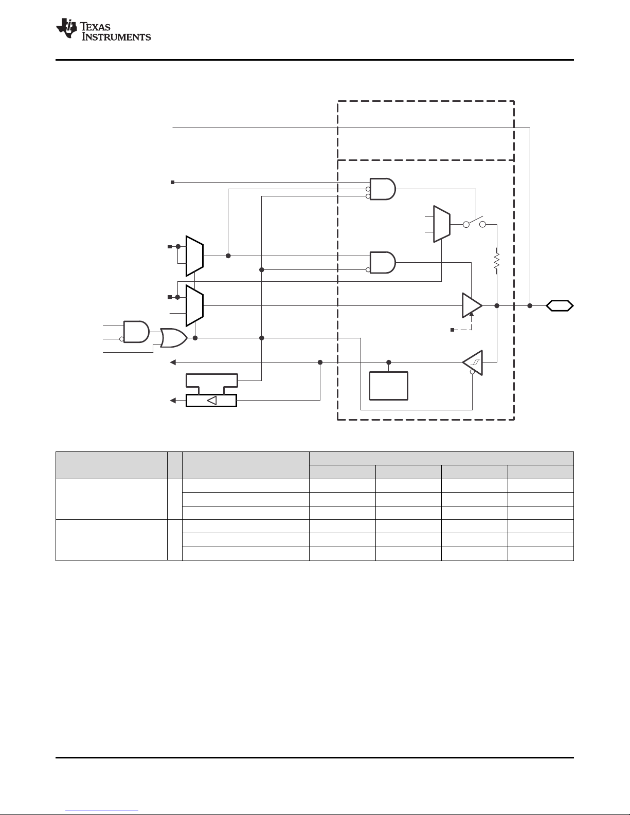
P5.3/XT2OUT
1
0
P5DIR.3
P5IN.3
EN
Module X IN
1
0
Module X OUT
P5OUT.3
1
0
DV
SS
DV
CC
P5REN.3
Pad Logic
1
P5DS.3
0: Low drive
1: High drive
D
Bus
Keeper
To XT2
P5SEL.2
XT2BYPASS
P5SEL.3
MSP430F5529,MSP430F5528,MSP430F5527,MSP430F5526
MSP430F5525,MSP430F5524,MSP430F5522,MSP430F5521
MSP430F5519, MSP430F5517, MSP430F5515, MSP430F5514, MSP430F5513
www.ti.com
6.10.7 Port P5, P5.3, Input/Output With Schmitt Trigger
SLAS590M –MARCH 2009–REVISED NOVEMBER 2015
Table 6-51. Port P5 (P5.2, P5.3) Pin Functions
PIN NAME (P5.x) x FUNCTION
P5.2/XT2IN 2 P5.2 (I/O) I: 0; O: 1 0 X X
XT2IN crystal mode
P5.3/XT2OUT 3 P5.3 (I/O) I: 0; O: 1 0 0 X
(1) X = Don't care
(2) Setting P5SEL.2 causes the general-purpose I/O to be disabled. Pending the setting of XT2BYPASS, P5.2 is configured for crystal
mode or bypass mode.
(3) Setting P5SEL.2 causes the general-purpose I/O to be disabled in crystal mode. When using bypass mode, P5.3 can be used as
general-purpose I/O.
Copyright © 2009–2015, Texas Instruments Incorporated Detailed Description 89
Product Folder Links: MSP430F5529 MSP430F5528 MSP430F5527 MSP430F5526 MSP430F5525 MSP430F5524
MSP430F5522 MSP430F5521 MSP430F5519 MSP430F5517 MSP430F5515 MSP430F5514 MSP430F5513
XT2IN bypass mode
XT2OUT crystal mode
P5.3 (I/O)
CONTROL BITS OR SIGNALS
(1)
P5DIR.x P5SEL.2 P5SEL.3 XT2BYPASS
(2)
(2)
(3)
(3)
Submit Documentation Feedback
X 1 X 0
X 1 X 1
X 1 X 0
X 1 0 1
Page 90

P5.4/XIN
P5SEL.4
1
0
P5DIR.4
P5IN.4
EN
ModuleXIN
1
0
ModuleXOUT
P5OUT.4
1
0
DV
SS
DV
CC
P5REN.4
PadLogic
1
P5DS.4
0:Lowdrive
1:Highdrive
D
Bus
Keeper
toXT1
MSP430F5529,MSP430F5528,MSP430F5527,MSP430F5526
MSP430F5525,MSP430F5524,MSP430F5522,MSP430F5521
MSP430F5519, MSP430F5517, MSP430F5515, MSP430F5514, MSP430F5513
SLAS590M –MARCH 2009–REVISED NOVEMBER 2015
6.10.7.1 Port P5, P5.4 and P5.5 Input/Output With Schmitt Trigger
www.ti.com
90 Detailed Description Copyright © 2009–2015, Texas Instruments Incorporated
Product Folder Links: MSP430F5529 MSP430F5528 MSP430F5527 MSP430F5526 MSP430F5525 MSP430F5524
MSP430F5522 MSP430F5521 MSP430F5519 MSP430F5517 MSP430F5515 MSP430F5514 MSP430F5513
Submit Documentation Feedback
Page 91

P5.5/XOUT
1
0
P5DIR.5
P5IN.5
EN
Module X IN
1
0
Module X OUT
P5OUT.5
1
0
DV
SS
DV
CC
P5REN.5
Pad Logic
1
P5DS.5
0: Low drive
1: High drive
D
Bus
Keeper
to XT1
P5SEL.4
XT1BYPASS
P5SEL.5
www.ti.com
MSP430F5529,MSP430F5528,MSP430F5527,MSP430F5526
MSP430F5525,MSP430F5524,MSP430F5522,MSP430F5521
MSP430F5519, MSP430F5517, MSP430F5515, MSP430F5514, MSP430F5513
SLAS590M –MARCH 2009–REVISED NOVEMBER 2015
Table 6-52. Port P5 (P5.4 and P5.5) Pin Functions
PIN NAME (P5.x) x FUNCTION
P5.4/XIN 4 P5.4 (I/O) I: 0; O: 1 0 X X
XIN crystal mode
XIN bypass mode
P5.5/XOUT 5 P5.5 (I/O) I: 0; O: 1 0 0 X
(1) X = Don't care
(2) Setting P5SEL.4 causes the general-purpose I/O to be disabled. Pending the setting of XT1BYPASS, P5.4 is configured for crystal
mode or bypass mode.
(3) Setting P5SEL.4 causes the general-purpose I/O to be disabled in crystal mode. When using bypass mode, P5.5 can be used as
general-purpose I/O.
Copyright © 2009–2015, Texas Instruments Incorporated Detailed Description 91
Product Folder Links: MSP430F5529 MSP430F5528 MSP430F5527 MSP430F5526 MSP430F5525 MSP430F5524
MSP430F5522 MSP430F5521 MSP430F5519 MSP430F5517 MSP430F5515 MSP430F5514 MSP430F5513
XOUT crystal mode
P5.5 (I/O)
CONTROL BITS OR SIGNALS
(1)
P5DIR.x P5SEL.4 P5SEL.5 XT1BYPASS
(2)
(2)
(3)
(3)
Submit Documentation Feedback
X 1 X 0
X 1 X 1
X 1 X 0
X 1 0 1
Page 92

P5.6/TB0.0
P5.7/TB0.1
Direction
0:Input
1:Output
P5SEL.x
1
0
P5DIR.x
P5IN.x
EN
Tomodule
1
0
FromModule
P5OUT.x
1
0
DV
SS
DV
CC
P5REN.x
PadLogic
1
P5DS.x
0:Lowdrive
1:Highdrive
D
MSP430F5529,MSP430F5528,MSP430F5527,MSP430F5526
MSP430F5525,MSP430F5524,MSP430F5522,MSP430F5521
MSP430F5519, MSP430F5517, MSP430F5515, MSP430F5514, MSP430F5513
SLAS590M –MARCH 2009–REVISED NOVEMBER 2015
6.10.8 Port P5, P5.6 to P5.7, Input/Output With Schmitt Trigger
www.ti.com
Table 6-53. Port P5 (P5.6 to P5.7) Pin Functions
PIN NAME (P5.x) x FUNCTION
P5.6/TB0.0
P5.7/TB0.1
(1) F5529, F5527, F5525, F5521, F5519, F5517, F5515 devices only.
(1)
6 P5.6 (I/O) I: 0; O: 1 0
TB0.CCI0A 0 1
TB0.0 1 1
(1)
7 TB0.CCI1A 0 1
TB0.1 1 1
CONTROL BITS OR SIGNALS
P5DIR.x P5SEL.x
92 Detailed Description Copyright © 2009–2015, Texas Instruments Incorporated
Product Folder Links: MSP430F5529 MSP430F5528 MSP430F5527 MSP430F5526 MSP430F5525 MSP430F5524
MSP430F5522 MSP430F5521 MSP430F5519 MSP430F5517 MSP430F5515 MSP430F5514 MSP430F5513
Submit Documentation Feedback
Page 93

P6.0/CB0/(A0)
P6.1/CB1/(A1)
P6.2/CB2/(A2)
P6.3/CB3/(A3)
P6.4/CB4/(A4)
P6.5/CB5/(A5)
P6.6/CB6/(A6)
P6.7/CB7/(A7)
P6SEL.x
1
0
P6DIR.x
P6IN.x
EN
Tomodule
1
0
Frommodule
P6OUT.x
1
0
DVSS
DVCC
1
P6DS.x
0:Lowdrive
1:Highdrive
D
toComparator_B
fromComparator_B
PadLogic
to ADC12
INCHx=x
(n/aMSPF430F551x)
Bus
Keeper
Direction
0:Input
1:Output
CBPD.x
P6REN.x
(n/aMSPF430F551x)
MSP430F5529,MSP430F5528,MSP430F5527,MSP430F5526
MSP430F5525,MSP430F5524,MSP430F5522,MSP430F5521
MSP430F5519, MSP430F5517, MSP430F5515, MSP430F5514, MSP430F5513
www.ti.com
SLAS590M –MARCH 2009–REVISED NOVEMBER 2015
6.10.9 Port P6, P6.0 to P6.7, Input/Output With Schmitt Trigger
Copyright © 2009–2015, Texas Instruments Incorporated Detailed Description 93
Product Folder Links: MSP430F5529 MSP430F5528 MSP430F5527 MSP430F5526 MSP430F5525 MSP430F5524
MSP430F5522 MSP430F5521 MSP430F5519 MSP430F5517 MSP430F5515 MSP430F5514 MSP430F5513
Submit Documentation Feedback
Page 94

MSP430F5529,MSP430F5528,MSP430F5527,MSP430F5526
MSP430F5525,MSP430F5524,MSP430F5522,MSP430F5521
MSP430F5519, MSP430F5517, MSP430F5515, MSP430F5514, MSP430F5513
SLAS590M –MARCH 2009–REVISED NOVEMBER 2015
Table 6-54. Port P6 (P6.0 to P6.7) Pin Functions
www.ti.com
PIN NAME (P6.x) x FUNCTION
CONTROL BITS OR SIGNALS
P6DIR.x P6SEL.x CBPD
P6.0/CB0/(A0) 0 P6.0 (I/O) I: 0; O: 1 0 0
A0 (only MSP430F552x) X 1 X
(1)
CB0
X X 1
P6.1/CB1/(A1) 1 P6.1 (I/O) I: 0; O: 1 0 0
A1 (only MSP430F552x) X 1 X
(1)
CB1
X X 1
P6.2/CB2/(A2) 2 P6.2 (I/O) I: 0; O: 1 0 0
A2 (only MSP430F552x) X 1 X
(1)
CB2
X X 1
P6.3/CB3/(A3) 3 P6.3 (I/O) I: 0; O: 1 0 0
A3 (only MSP430F552x) X 1 X
(1)
CB3
X X 1
P6.4/CB4/(A4) 4 P6.4 (I/O) I: 0; O: 1 0 0
A4 (only MSP430F552x) X 1 X
(1)
CB4
X X 1
P6.5/CB5/(A5) 5 P6.5 (I/O) I: 0; O: 1 0 0
A5 (only MSP430F552x) X 1 X
(1)
CB5
X X 1
P6.6/CB6/(A6) 6 P6.6 (I/O) I: 0; O: 1 0 0
A6 (only MSP430F552x) X 1 X
(1)
CB6
X X 1
P6.7/CB7/(A7) 7 P6.7 (I/O) I: 0; O: 1 0 0
A7 (only MSP430F552x) X 1 X
(1)
CB7
X X 1
(1) Setting the CBPD.x bit disables the output driver and the input Schmitt trigger to prevent parasitic cross currents when applying analog
signals. Selecting the CBx input pin to the comparator multiplexer with the CBx bits automatically disables output driver and input buffer
for that pin, regardless of the state of the associated CBPD.x bit.
94 Detailed Description Copyright © 2009–2015, Texas Instruments Incorporated
Product Folder Links: MSP430F5529 MSP430F5528 MSP430F5527 MSP430F5526 MSP430F5525 MSP430F5524
MSP430F5522 MSP430F5521 MSP430F5519 MSP430F5517 MSP430F5515 MSP430F5514 MSP430F5513
Submit Documentation Feedback
Page 95

P7.0/CB8/(A12)
P7.1/CB9/(A13)
P7.2/CB10/(A14)
P7.3/CB11/(A15)
P7SEL.x
1
0
P7DIR.x
P7IN.x
EN
Tomodule
1
0
Frommodule
P7OUT.x
1
0
DVSS
DVCC
1
P7DS.x
0:Lowdrive
1:Highdrive
D
toComparator_B
fromComparator_B
PadLogic
to ADC12
(n/aMSPF430F551x)
INCHx=x
(n/aMSPF430F551x)
Bus
Keeper
Direction
0:Input
1:Output
CBPD.x
P7REN.x
MSP430F5529,MSP430F5528,MSP430F5527,MSP430F5526
MSP430F5525,MSP430F5524,MSP430F5522,MSP430F5521
MSP430F5519, MSP430F5517, MSP430F5515, MSP430F5514, MSP430F5513
www.ti.com
SLAS590M –MARCH 2009–REVISED NOVEMBER 2015
6.10.10 Port P7, P7.0 to P7.3, Input/Output With Schmitt Trigger
Copyright © 2009–2015, Texas Instruments Incorporated Detailed Description 95
Product Folder Links: MSP430F5529 MSP430F5528 MSP430F5527 MSP430F5526 MSP430F5525 MSP430F5524
MSP430F5522 MSP430F5521 MSP430F5519 MSP430F5517 MSP430F5515 MSP430F5514 MSP430F5513
Submit Documentation Feedback
Page 96

MSP430F5529,MSP430F5528,MSP430F5527,MSP430F5526
MSP430F5525,MSP430F5524,MSP430F5522,MSP430F5521
MSP430F5519, MSP430F5517, MSP430F5515, MSP430F5514, MSP430F5513
SLAS590M –MARCH 2009–REVISED NOVEMBER 2015
Table 6-55. Port P7 (P7.0 to P7.3) Pin Functions
www.ti.com
PIN NAME (P7.x) x FUNCTION
P7.0/CB8/(A12) 0 P7.0 (I/O)
A12
CB8
P7.1/CB9/(A13) 1 P7.1 (I/O)
A13
CB9
P7.2/CB10/(A14) 2 P7.2 (I/O)
A14
CB10
P7.3/CB11/(A15) 3 P7.3 (I/O)
A15
CB11
(1)
(2)
(3) (1)
(1)
(2)
(3) (1)
(1)
(2)
(3) (1)
(1)
(2)
(3) (1)
CONTROL BITS OR SIGNALS
P7DIR.x P7SEL.x CBPD
I: 0; O: 1 0 0
X 1 X
X X 1
I: 0; O: 1 0 0
X 1 X
X X 1
I: 0; O: 1 0 0
X 1 X
X X 1
I: 0; O: 1 0 0
X 1 X
X X 1
(1) F5529, F5527, F5525, F5521, F5519, F5517, F5515 devices only
(2) F5529, F5527, F5525, F5521 devices only
(3) Setting the CBPD.x bit disables the output driver and the input Schmitt trigger to prevent parasitic cross currents when applying analog
signals. Selecting the CBx input pin to the comparator multiplexer with the CBx bits automatically disables output driver and input buffer
for that pin, regardless of the state of the associated CBPD.x bit.
96 Detailed Description Copyright © 2009–2015, Texas Instruments Incorporated
Product Folder Links: MSP430F5529 MSP430F5528 MSP430F5527 MSP430F5526 MSP430F5525 MSP430F5524
MSP430F5522 MSP430F5521 MSP430F5519 MSP430F5517 MSP430F5515 MSP430F5514 MSP430F5513
Submit Documentation Feedback
Page 97

P7.4/TB0.2
P7.5/TB0.3
P7.6/TB0.4
P7.7/TB0CLK/MCLK
Direction
0:Input
1:Output
P7SEL.x
1
0
P7DIR.x
P7IN.x
EN
Tomodule
1
0
Frommodule
P7OUT.x
1
0
DV
SS
DV
CC
P7REN.x
PadLogic
1
P7DS.x
0:Lowdrive
1:Highdrive
D
MSP430F5529,MSP430F5528,MSP430F5527,MSP430F5526
MSP430F5525,MSP430F5524,MSP430F5522,MSP430F5521
MSP430F5519, MSP430F5517, MSP430F5515, MSP430F5514, MSP430F5513
www.ti.com
SLAS590M –MARCH 2009–REVISED NOVEMBER 2015
6.10.11 Port P7, P7.4 to P7.7, Input/Output With Schmitt Trigger
Table 6-56. Port P7 (P7.4 to P7.7) Pin Functions
PIN NAME (P7.x) x FUNCTION
P7.4/TB0.2
P7.5/TB0.3
P7.6/TB0.4
P7.7/TB0CLK/MCLK
(1) F5529, F5527, F5525, F5521, F5519, F5517, F5515 devices only
(1)
4 P7.4 (I/O) I: 0; O: 1 0
TB0.CCI2A 0 1
TB0.2 1 1
(1)
5 P7.5 (I/O) I: 0; O: 1 0
TB0.CCI3A 0 1
TB0.3 1 1
(1)
6 P7.6 (I/O) I: 0; O: 1 0
TB0.CCI4A 0 1
TB0.4 1 1
(1)
7 P7.7 (I/O) I: 0; O: 1 0
TB0CLK 0 1
MCLK 1 1
CONTROL BITS OR SIGNALS
P7DIR.x P7SEL.x
Copyright © 2009–2015, Texas Instruments Incorporated Detailed Description 97
Product Folder Links: MSP430F5529 MSP430F5528 MSP430F5527 MSP430F5526 MSP430F5525 MSP430F5524
MSP430F5522 MSP430F5521 MSP430F5519 MSP430F5517 MSP430F5515 MSP430F5514 MSP430F5513
Submit Documentation Feedback
Page 98

P8.0
P8.1
P8.2
Direction
0:Input
1:Output
P8SEL.x
1
0
P8DIR.x
P8IN.x
EN
toPortMappingControl
1
0
fromPortMappingControl
P8OUT.x
1
0
DV
SS
DV
CC
P8REN.x
PadLogic
1
P8DS.x
0:Lowdrive
1:Highdrive
D
fromPortMappingControl
MSP430F5529,MSP430F5528,MSP430F5527,MSP430F5526
MSP430F5525,MSP430F5524,MSP430F5522,MSP430F5521
MSP430F5519, MSP430F5517, MSP430F5515, MSP430F5514, MSP430F5513
SLAS590M –MARCH 2009–REVISED NOVEMBER 2015
6.10.12 Port P8, P8.0 to P8.2, Input/Output With Schmitt Trigger
www.ti.com
PIN NAME (P8.x) x FUNCTION
(1)
P8.0
(1)
P8.1
(1)
P8.2
(1) F5529, F5527, F5525, F5521, F5519, F5517, F5515 devices only
Table 6-57. Port P8 (P8.0 to P8.2) Pin Functions
CONTROL BITS OR SIGNALS
P8DIR.x P8SEL.x
0 P8.0(I/O) I: 0; O: 1 0
1 P8.1(I/O) I: 0; O: 1 0
2 P8.2(I/O) I: 0; O: 1 0
98 Detailed Description Copyright © 2009–2015, Texas Instruments Incorporated
Product Folder Links: MSP430F5529 MSP430F5528 MSP430F5527 MSP430F5526 MSP430F5525 MSP430F5524
MSP430F5522 MSP430F5521 MSP430F5519 MSP430F5517 MSP430F5515 MSP430F5514 MSP430F5513
Submit Documentation Feedback
Page 99

PUOPE 0
1
0
1
PUOUT0
PUSEL
PadLogic
PU.0
/
DP
VUSB VSSU
PU.1/
DM
0
1
PUOUT
1
.
PUIN1
USBDMinput
PUIN0
USBDP input
USBDMoutput
USBDP output
PUSEL
PadLogic
PUR
VUSB VSSU
“1”
PUREN
PURIN
PUIPE
MSP430F5529,MSP430F5528,MSP430F5527,MSP430F5526
MSP430F5525,MSP430F5524,MSP430F5522,MSP430F5521
MSP430F5519, MSP430F5517, MSP430F5515, MSP430F5514, MSP430F5513
www.ti.com
6.10.13 Port PU.0/DP, PU.1/DM, PUR USB Ports
SLAS590M –MARCH 2009–REVISED NOVEMBER 2015
Copyright © 2009–2015, Texas Instruments Incorporated Detailed Description 99
Product Folder Links: MSP430F5529 MSP430F5528 MSP430F5527 MSP430F5526 MSP430F5525 MSP430F5524
MSP430F5522 MSP430F5521 MSP430F5519 MSP430F5517 MSP430F5515 MSP430F5514 MSP430F5513
Submit Documentation Feedback
Page 100

MSP430F5529,MSP430F5528,MSP430F5527,MSP430F5526
MSP430F5525,MSP430F5524,MSP430F5522,MSP430F5521
MSP430F5519, MSP430F5517, MSP430F5515, MSP430F5514, MSP430F5513
SLAS590M –MARCH 2009–REVISED NOVEMBER 2015
www.ti.com
(1)
(1)
DP
(2)
Table 6-58. Port PU.0/DP, PU.1/DM Output Functions
CONTROL BITS PIN NAME
PUSEL PUOPE PUOUT1 PUOUT0 PU.1/DM PU.0/DP
0 0 X X Output disabled Output disabled
0 1 0 0 Output low Output low
0 1 0 1 Output low Output high
0 1 1 0 Output high Output low
0 1 1 1 Output high Output high
1 X X X DM
(1) PU.1/DM and PU.0/DP inputs and outputs are supplied from VUSB. VUSB can be generated by the
device using the integrated 3.3-V LDO when enabled. VUSB can also be supplied externally when the
3.3-V LDO is not being used and is disabled.
(2) Output state set by the USB module.
(2)
Table 6-59. Port PU.0/DP, PU.1/DM Input Functions
CONTROL BITS PIN NAME
PUSEL PUIPE PU.1/DM PU.0/DP
0 0 Input disabled Input disabled
0 1 Input enabled Input enabled
1 X DM input DP input
(1) PU.1/DM and PU.0/DP inputs and outputs are supplied from VUSB. VUSB can be generated by the
device using the integrated 3.3-V LDO when enabled. VUSB can also be supplied externally when the
3.3-V LDO is not being used and is disabled.
Table 6-60. Port PUR Input Functions
CONTROL BITS
PUSEL PUREN
0 0
0 1
1 0
1 1
FUNCTION
Input disabled
Pullup disabled
Input disabled
Pullup enabled
Input enabled
Pullup disabled
Input enabled
Pullup enabled
100 Detailed Description Copyright © 2009–2015, Texas Instruments Incorporated
Product Folder Links: MSP430F5529 MSP430F5528 MSP430F5527 MSP430F5526 MSP430F5525 MSP430F5524
MSP430F5522 MSP430F5521 MSP430F5519 MSP430F5517 MSP430F5515 MSP430F5514 MSP430F5513
Submit Documentation Feedback
 Loading...