

Page 1

MSP430F42xA
MIXED SIGNAL MICROCONTROLLER
SLAS587 -- FEBRUARY 2008
D Low Supply-Voltage Range, 1.8 V to 3.6 V
D Ultra-Low Power Consumption:
-- Active Mode: 400 μAat1MHz,3.0V
-- Standby Mode: 1.6 μA
-- Off Mode (RAM Retention): 0.1 μA
D Five Power-Saving Modes
D Wake-Up From Standby Mode in Less
Than 6 μs
D Frequency-Locked Loop, FLL+
D 16-Bit RISC Architecture, 125-ns
Instruction Cycle Time
D Three Independent 16-bit Sigma-Delta A/D
Converters With Differential PGA Inputs
D 16-Bit Timer_A With Three
Capture/Compare Registers
D Integrated LCD Driver for 128 Segments
D Serial Communication Interface (USART),
Asynchronous UART, or Synchronous SPI
Selectable by Software
D Brownout Detector
description
D Supply Voltage Supervisor/Monitor With
Programmable Level Detection
D Serial Onboard Programming,
No External Programming Voltage Needed,
Programmable Code Protection by Security
Fuse
D Bootstrap Loader in Flash Devices
D Family Members Include:
-- MSP430F423A:
8KB + 256B Flash Memory,
256B RAM
-- MSP430F425A:
16KB + 256B Flash Memory,
512B RAM
-- MSP430F427A:
32KB + 256B Flash Memory,
1KB RAM
D Availablein64-PinQuadFlatPack(QFP)
D For Complete Module Descriptions, Refer
to the MSP430x4xx Family User’s Guide,
Literature Number SLAU056
The Texas Instruments MSP430family ofultra-low power microcontrollers consists of several devices featuring
different sets of peripherals targeted for various applications. The architecture, combined with five low-power
modes, is optimized to achieve extended battery life in portable measurement applications. The device features
a powerful 16-bit RISC CPU, 16-bit registers, and constant generators that contribute to maximum code
efficiency. Thedigitally controlled oscillator (DCO) allows wake-up from low-power modesto activemode in less
than 6 μs.
The MSP430F42xA series are microcontroller configurations with three independent 16-bit sigma-delta A/D
converters, each with an integrated differential programmable gain amplifier input stage. Also included are a
built-in 16-bit timer, 128 LCD segment drive capability, hardware multiplier, and 14 I/O pins.
Typical applications include high-resolution applications such as handheld metering equipment, weigh scales,
and energy meters.
This integrated circuit can be damaged by ESD. Texas Instruments recommends that all integrated circuits be handled with
appropriate precautions. Failure to observe proper handling and installation procedures cancause damage. ESD damagecan range
from subtle performance degradation to complete device failure. Precision integrated circuits may be more susceptible to damage
because very small parametric changes could cause the device not to meet its published specifications. These devices have limited
built-in ESD protection.
Please be aware that an important notice concerning availability, standard warranty, and use in critical applications of
Texas Instruments semiconductor products and disclaimers thereto appears at the end of this data sheet.
PRODUCTION DATA information is current as of publication date.
Products conform to specifications per the terms of Texas Instruments
standard warranty. Production processing does not necessarily include
testing of all parameters.
POST OFFICE BOX 655303 • DALLAS, TEXAS 75265
Copyright © 2008 Texas Instruments Incorporated
1
Page 2
MSP430F42xA
0
MIXED SIGNAL MICROCONTROLLER
SLAS587 -- FEBRUARY 2008
T
A
-- 4 0 °Cto85°C
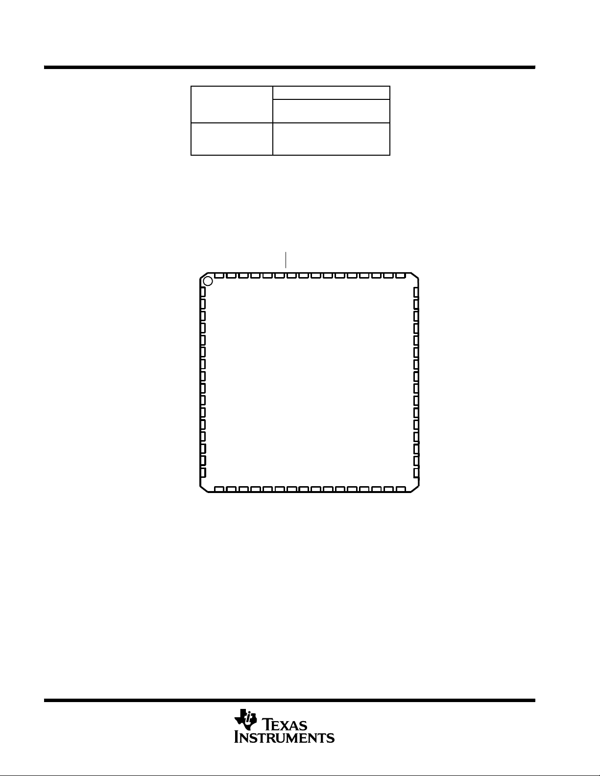
AVAILABLE OPTIONS
PACKAGED DEVICES
PLASTIC 64-PIN QFP
(PM)
MSP430F423AIPM
MSP430F425AIPM
MSP430F427AIPM
pin designation
†
DV
CC
A0.0+
A0.0-A1.0+
A1.0-A2.0+
A2.0--
XIN
XOUT
V
REF
P2.2/STE0
S0
S1
S2
S3
S4
SS
SS
CC
DV
AV
AV
64 63 62 61 60 59 58 57 56 55 54 53 52 51 50 49
1
2
3
4
5
6
7
8
9
10
11
12
13
14
15
16
17 18 19 20 21 22 23 24 25 26 27 28 29 30 31 32
P2.3/SVSIN
P2.4/UTXD0
P2.5/URXD0
RST/NMI
MSP430F42xA
TCK
TMS
TDI/TCLK
TDO/TDI
P1.0/TA0
P1.1/TA0/MCLK
P1.2/TA1/S31
P1.3/SVSOUT/S3
P1.4/S29
P1.5/TACLK/ACLK/S28
48
P1.6/SIMO0/S27
47
P1.7/SOMI0/S26
46
P2.0/TA2/S25
45
P2.1/UCLK0/S24
44
R33
43
R23
42
R13
41
R03
40
COM3
39
COM2
38
COM1
37
COM0
36
S23
35
S22
34
S21
33
S5S6S7S8S9
†
It is recommended to short unused analog input pairs and connect them to analog ground.
2
POST OFFICE BOX 655303 • DALLAS, TEXAS 75265
S10
S11
S12
S13
S14
S15
S16
S17
S18
S19
S20
Page 3
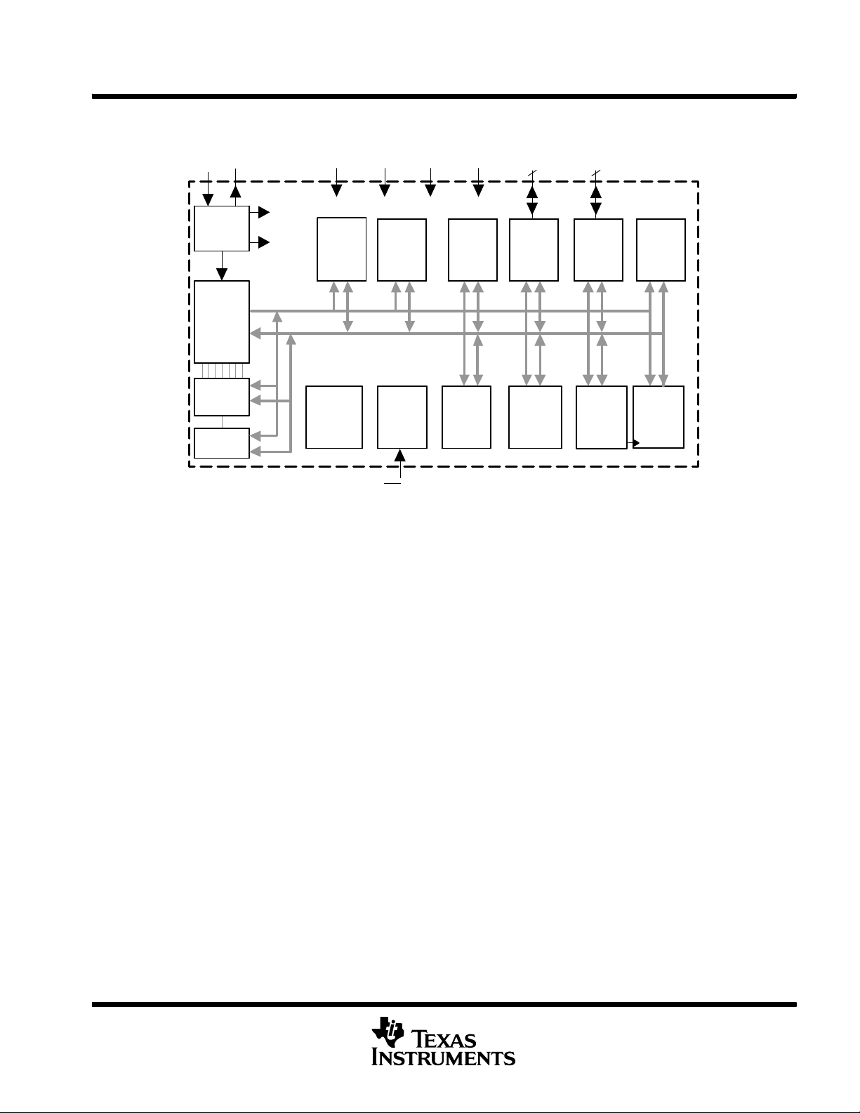
functional block diagram
MSP430F42xA
MIXED SIGNAL MICROCONTROLLER
SLAS587 -- FEBRUARY 2008
XOUT
XIN
Oscillators
FLL+
MCLK
8MHz
CPU
incl. 16
Registers
Emulation
Module
JTAG
Interface
ACLK
SMCLK
MAB
MDB
Hardware
Multiplier
MPY, MPYS
MAC,MACS
DV
Flash
32KB
16KB
8KB
DV
CC
SS
RAM
1KB
512B
256B
POR/
SVS/
Brownout
RST/NMI
AV
CC
AV
Timer_A3
3CCReg
Watchdog
WDT+
15/16-Bit
SS
P1
8
Port 1
8 I/O
Interrupt
Capability
SD16
Three 16-bit
Sigma-Delta
A/D
Converters
P2
6
Port 2
6 I/O
Interrupt
Capability
Basic
Timer 1
1 Interrupt
Vector
USART0
UART or
Function
Segments
1,2,3,4 MUX
f
LCD
SPI
LCD
128
POST OFFICE BOX 655303 • DALLAS, TEXAS 75265
3
Page 4
MSP430F42xA
/
MIXED SIGNAL MICROCONTROLLER
SLAS587 -- FEBRUARY 2008
Terminal Functions
TERMINAL
NAME NO.
DV
CC
A0.0+ 2 I Internal connection to SD16 Channel 0, input 0 +. (see Note 1)
A0.0-- 3 I Internal connection to SD16 Channel 0, input 0 --. (see Note 1)
A1.0+ 4 I Internal connection to SD16 Channel 1, input 0 +. (see Note 1)
A1.0-- 5 I Internal connection to SD16 Channel 1, input 0 --. (see Note 1)
A2.0+ 6 I Internal connection to SD16 Channel 2, input 0 +. (see Note 1)
A2.0-- 7 I Internal connection to SD16 Channel 2, input 0 --. (see Note 1)
XIN 8 I Input port for crystal oscillator XT1. Standard or watch crystals can be connected.
XOUT 9 O Output terminal of crystal oscillator XT1
V
REF
P2.2/STE0 11 I/O General-purpose digital I/O / slave transmit enable—USART0/SPI mode
S0 12 O LCD segment output 0
S1 13 O LCD segment output 1
S2 14 O LCD segment output 2
S3 15 O LCD segment output 3
S4 16 O LCD segment output 4
S5 17 O LCD segment output 5
S6 18 O LCD segment output 6
S7 19 O LCD segment output 7
S8 20 O LCD segment output 8
S9 21 O LCD segment output 9
S10 22 O LCD segment output 10
S11 23 O LCD segment output 11
S12 24 O LCD segment output 12
S13 25 O LCD segment output 13
S14 26 O LCD segment output 14
S15 27 O LCD segment output 15
S16 28 O LCD segment output 16
S17 29 O LCD segment output 17
S18 30 O LCD segment output 18
S19 31 O LCD segment output 19
S20 32 O LCD segment output 20
S21 33 O LCD segment output 21
S22 34 O LCD segment output 22
S23 35 O LCD segment output 23
COM0 36 O Common output, COM0--3 are used for LCD backplanes.
COM1 37 O Common output, COM0--3 are used for LCD backplanes.
COM2 38 O Common output, COM0--3 are used for LCD backplanes.
COM3 39 O Common output, COM0--3 are used for LCD backplanes.
R03 40 I Input port of fourth positive (lowest) analog LCD level (V5)
I
O DESCRIPTION
1 Digital supply voltage, positive terminal.
10 I/O Input for an external reference voltage / internal reference voltage output (can be used as mid-voltage)
NOTE 1: It is recommended to short unused analog input pairs and connect them to analog ground.
4
POST OFFICE BOX 655303 • DALLAS, TEXAS 75265
Page 5
MIXED SIGNAL MICROCONTROLLER
/
Terminal Functions (Continued)
MSP430F42xA
SLAS587 -- FEBRUARY 2008
TERMINAL
NAME NO.
R13 41 I Input port of third most positive analog LCD level (V4 or V3)
R23 42 I Input port of second most positive analog LCD level (V2)
R33 43 O Output port of most positive analog LCD level (V1)
P2.1/UCLK0/S24 44 I/O
P2.0/TA2/S25 45 I/O
P1.7/SOMI0/S26 46 I/O
P1.6/SIMO0/S27 47 I/O
P1.5/TACLK/
ACLK/S28
P1.4/S29 49 I/O General-purpose digital I/O / LCD segment output 29 (See Note 1)
P1.3/SVSOUT/
S30
P1.2/TA1/S31 51 I/O
P1.1/TA0/MCLK 52 I/O
P1.0/TA0 53 I/O General-purpose digital I/O / Timer_A, Capture: CCI0A input, Compare: Out0 output / BSL transmit
TDO/TDI 54 I/O Test data output port. TDO/TDI data output or programming data input terminal.
TDI/TCLK 55 I Test data input or test clock input. The device protection fuse is connected to TDI.
TMS 56 I Test mode select. TMS is used as an input port for device programming and test.
TCK 57 I Test clock. TCK is the clock input port for device programming and test.
RST/NMI 58 I Reset input or nonmaskable interrupt input port
P2.5/URXD0 59 I/O General-purpose digital I/O / receive data in—USART0/UART mode
P2.4/UTXD0 60 I/O General-purpose digital I/O / transmit data out—USART0/UART mode
P2.3/SVSIN 61 I/O General-purpose digital I/O / Analog input to brownout, supply voltage supervisor
AV
SS
DV
SS
AV
CC
I
O DESCRIPTION
General-purpose digital I/O/ external clock input-USART0/UART orSPI mode, clock output—USART0/SPI
mode / LCD segment output 24 (See Note 1)
General-purpose digital I/O / Timer_A Capture: CCI2A input, Compare: Out2 output / LCD segment output
25 (See Note 1)
General-purpose digital I/O / slave out/master in of USART0/SPI mode / LCD segment output 26
(See Note 1)
General-purpose digital I/O / slave in/master out of USART0/SPI mode / LCD segment output 27
(See Note 1)
48 I/O
50 I/O General-purpose digital I/O / SVS: output of SVS comparator / LCD segment output 30 (See Note 1)
62
63 Digital supply voltage, negative terminal
64
General-purpose digital I/O / Timer_A and SD16 clock signal TACLK input / ACLK output (divided by 1,
2, 4, or 8) / LCD segment output 28 (See Note 1)
General-purpose digital I/O/ Timer_A, Capture: CCI1A, CCI1B input, Compare: Out1 output / LCD segment
output 31 (See Note 1)
General-purpose digital I/O / Timer_A, Capture: CCI0B input / MCLK output.
Note: TA0 is only an input on this pin / BSL receive
Analog supply voltage, negative terminal. Supplies SD16, SVS, brownout, oscillator, and LCD resistive
divider circuitry.
Analog supply voltage, positive terminal. Supplies SD16, SVS, brownout, oscillator, and LCD resistive
divider circuitry; must not power up prior to DV
CC
.
NOTE 1: LCD function is selected automatically when applicable LCD module control bits are set, not with PxSEL bits.
POST OFFICE BOX 655303 • DALLAS, TEXAS 75265
5
Page 6
MSP430F42xA
MIXED SIGNAL MICROCONTROLLER
SLAS587 -- FEBRUARY 2008
short-form description
CPU
The MSP430 CPU has a 16-bit RISC architecture
that is highly transparent to the application. All
operations, other than program-flow instructions,
are performed as register operations in
conjunction with seven addressing modes for the
source operand and four addressing modes for
the destination operand.
The CPU is integrated with 16 registers that
provide reduced instruction execution time. The
register-to-register operation execution time is
one cycle of the CPU clock.
Four of the registers, R0 to R3, are dedicated as
program counter, stack pointer, status register,
and constant generator, respectively. The
remaining registers are general-purpose
registers.
Peripherals are connected to the CPU using data,
address, and control buses, and can be handled
with all instructions.
instruction set
The instruction set consists of 51 instructions with
three formats and seven address modes. Each
instruction can operate on word and byte data.
Table 1 shows examples of the three types of
instruction formats; the address modes are listed
in Table 2.
Program Counter
Stack Pointer
Status Register
Constant Generator
General-Purpose Register
General-Purpose Register
General-Purpose Register
General-Purpose Register
General-Purpose Register
General-Purpose Register
General-Purpose Register
General-Purpose Register
General-Purpose Register
General-Purpose Register
General-Purpose Register
General-Purpose Register
PC/R0
SP/R1
SR/CG1/R2
CG2/R3
R4
R5
R6
R7
R8
R9
R10
R11
R12
R13
R14
R15
Table 1. Instruction Word Formats
Dual operands, source-destination e.g., ADD R4,R5 R4 + R5 ------> R5
Single operands, destination only e.g., CALL R8 PC -- -->(TOS), R8----> PC
Relative jump, un/conditional e.g., JNE Jump-on-equal bit = 0
Table 2. Address Mode Descriptions
ADDRESS MODE S D SYNTAX EXAMPLE OPERATION
Register D
Indexed D D MOV X(Rn),Y(Rm) MOV 2(R5),6(R6) M(2+R5)-- --> M(6+R6)
Symbolic (PC relative) D D MOV EDE,TONI M(EDE) ----> M(TONI)
Absolute D D MOV &MEM,&TCDAT M(MEM) -- --> M(TCDAT)
Indirect D MOV @Rn,Y(Rm) MOV @R10,Tab(R6) M(R10) -- --> M(Tab+R6)
Indirect
autoincrement
Immediate D MOV #X,TONI MOV #45,TONI #45 ----> M(TONI)
NOTE: S = source D = destination
D
D MOV @Rn+,Rm MOV @R10+,R11
MOV Rs,Rd MOV R10,R11 R10 ----> R11
M(R10) -- --> R11
R10 + 2----> R10
6
POST OFFICE BOX 655303 • DALLAS, TEXAS 75265
Page 7

MSP430F42xA
MIXED SIGNAL MICROCONTROLLER
SLAS587 -- FEBRUARY 2008
operating modes
The MSP430 has one active mode and five software-selectable low-power modes of operation. An interrupt
event can wake up the device from any of the five low-power modes, service the request, and restore back to
the low-power mode on return from the interrupt program.
The following six operating modes can be configured by software:
D Active mode (AM)
-- All clocks are active.
D Low-power mode 0 (LPM0)
-- CPU is disabled.
ACLK and SMCLK remain active, MCLK is available to modules.
FLL+ loop control remains active.
D Low-power mode 1 (LPM1)
-- CPU is disabled.
ACLK and SMCLK remain active, MCLK is available to modules.
FLL+ loop control is disabled.
D Low-power mode 2 (LPM2)
-- CPU is disabled.
MCLK, FLL+ loop control, and DCOCLK are disabled.
DCO dc generator remains enabled.
ACLK remains active.
D Low-power mode 3 (LPM3)
-- CPU is disabled.
MCLK, FLL+ loop control, and DCOCLK are disabled.
DCO dc generator is disabled.
ACLK remains active.
D Low-power mode 4 (LPM4)
-- CPU is disabled.
ACLK is disabled.
MCLK, FLL+ loop control, and DCOCLK are disabled.
DCO dc generator is disabled.
Crystal oscillator is stopped.
POST OFFICE BOX 655303 • DALLAS, TEXAS 75265
7
Page 8
MSP430F42xA
MIXED SIGNAL MICROCONTROLLER
SLAS587 -- FEBRUARY 2008
interrupt vector addresses
The interrupt vectors andthe power-upstarting address are located in the address range of0FFFFh to0FFE0h.
The vector contains the 16-bit address of the appropriate interrupt-handler instruction sequence.
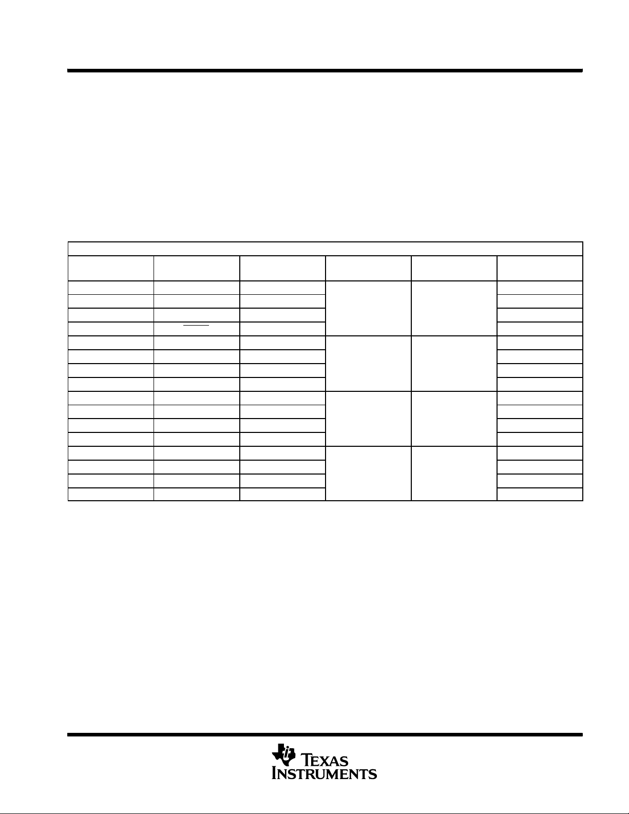
INTERRUPT SOURCE INTERRUPT FLAG SYSTEM INTERRUPT WORD ADDRESS PRIORITY
Power-up
External reset
Watchdog
Flash memory
PC out-of-range (see Note 4)
NMI
Oscillator fault
Flash memory access violation
SD16
Watchdog timer WDTIFG Maskable 0FFF4h 10
USART0 receive URXIFG0 Maskable 0FFF2h 9
USART0 transmit UTXIFG0 Maskable 0FFF0h 8
Timer_A3 TACCR0 CCIFG (see Note 2) Maskable 0FFECh 6
Timer_A3
I/O port P1 (eight flags)
I/O port P2 (eight flags)
Basic Timer1 BTIFG Maskable 0FFE0h 0, lowest
NOTES: 1. Multiple source flags
2. Interrupt flags are located in the module.
3. (Non)maskable: the individual interrupt-enable bit can disable an interrupt event, but the general interrupt-enable cannot.
4. A reset is generated if the CPU tries to fetch instructions from within the module register memory address range (0h to 01FFh) or
from within unused address ranges (from 0600h to 0BFFh).
NMIIFG (see Notes 1 and 3)
OFIFG (see Notes 1 and 3)
ACCVIFG (see Notes 1 and 3)
SD16CCTLx SD16OVIFG,
CCIFGs, and TACTL TAIFG
WDTIFG
KEYV
(see Note 1)
SD16CCTLx SD16IFG
(see Notes 1 and 2)
TACCR1 and TACCR2
(see Notes 1 and 2)
P1IFG.0toP1IFG.7
(see Notes 1 and 2)
P2IFG.0toP2IFG.7
(see Notes 1 and 2)
Reset 0FFFEh 15, highest
(Non)maskable
(Non)maskable
(Non)maskable
Maskable 0FFF8h 12
Maskable 0FFEAh 5
Maskable 0FFE8h 4
Maskable 0FFE2h 1
0FFFCh 14
0FFFAh 13
0FFF6h 11
0FFEEh 7
0FFE6h 3
0FFE4h 2
8
POST OFFICE BOX 655303 • DALLAS, TEXAS 75265
Page 9
MSP430F42xA
MIXED SIGNAL MICROCONTROLLER
SLAS587 -- FEBRUARY 2008
special function registers
Most interruptand module enable bits are collected into the lowest address space. Special function register bits
that are not allocated to a functional purpose are not physically present in the device. Simple software access
is provided with this arrangement.
interrupt enable 1 and 2
Address
0h URXIE0 ACCVIE NMIIE
7654 0
UTXIE0 OFIE WDTIE
rw–0 rw–0 rw–0
rw–0 rw–0 rw–0
32 1
WDTIE: Watchdog timer interruptenable. Inactive if watchdog modeis selected. Active if watchdogtimer
is configured in interval timer mode.
OFIE: Oscillator fault interrupt enable
NMIIE: Nonmaskable interrupt enable
ACCVIE: Flash access violation interrupt enable
URXIE0: USART0: UART and SPI receive-interrupt enable
UTXIE0: USART0: UART and SPI transmit-interrupt enable
Address
1h BTIE
BTIE: Basic Timer1 interrupt enable
7654 0321
rw-0
interrupt flag register 1 and 2
Address
02h URXIFG0 NMIIFG
7654 0
UTXIFG0 OFIFG WDTIFG
rw–1 rw–0
rw–0 rw–1 rw–(0)
32 1
WDTIFG: Set on watchdog timer overflow (in watchdog mode) or security key violation. Reset on V
power up or a reset condition at the RST/NMI pin in reset mode.
OFIFG: Flag set on oscillator fault
NMIIFG: Set via RST
/NMI pin
URXIFG0: USART0: UART and SPI receive flag
UTXIFG0: USART0: UART and SPI transmit flag
Address
3h BTIFG
BTIFG: Basic Timer1 interrupt flag
7654 0321
rw-0
CC
POST OFFICE BOX 655303 • DALLAS, TEXAS 75265
9
Page 10
MSP430F42xA
MIXED SIGNAL MICROCONTROLLER
SLAS587 -- FEBRUARY 2008
module enable registers 1 and 2
Address
04h
7654 0
UTXE0
rw–0 rw–0
URXE0
USPIE0
URXE0: USART0: UART mode receive enable
UTXE0: USART0: UART mode transmit enable
USPIE0: USART0: SPI mode transmit and receive enable
Address
05h
Legend: rw--0,1: Bit can be read and written. It Is reset or set by PUC.
7654 0321
rw--(0,1): Bit can be read and written. It Is reset or set by POR.
SFR Bit Not Present in Device.
memory organization
MSP430F423A MSP430F425A MSP430F427A
Memory
Interrupt vector
Code memory
Information memory Size 256 Byte
Boot memory Size 1kB
RAM Size 256 Byte
Peripherals 16 bit
Size
Flash
Flash
8bit
8-bit SFR
8KB
0FFFFh to 0FFE0h
0FFFFh to 0E000h
010FFh to 01000h
0FFFh to 0C00h
02FFh to 0200h
01FFh to 0100h
0FFh to 010h
0Fh to 00h
32 1
16KB
0FFFFh to 0FFE0h
0FFFFh to 0C000h
256 Byte
010FFh to 01000h
1kB
0FFFh to 0C00h
512 Byte
03FFh to 0200h
01FFh to 0100h
0FFh to 010h
0Fh to 00h
0FFFFh to 0FFE0h
0FFFFh to 08000h
256 Byte
010FFh to 01000h
0FFFh to 0C00h
05FFh to 0200h
01FFh to 0100h
0FFh to 010h
0Fh to 00h
32KB
1kB
1KB
bootstrap loader (BSL)
The MSP430 bootstrap loader (BSL) enables users to program the flash memory or RAM using a UART serial
interface. Access to the MSP430 memory via the BSL is protected by user-defined password. For complete
description of the features of the BSLand itsimplementation, see the application report Features of the MSP430
Bootstrap Loader, literature number SLAA089.
BSL FUNCTION PM PACKAGE PINS
Data transmit 53 - P1.0
Data receive 52 - P1.1
10
POST OFFICE BOX 655303 • DALLAS, TEXAS 75265
Page 11
MSP430F42xA
K
MIXED SIGNAL MICROCONTROLLER
SLAS587 -- FEBRUARY 2008
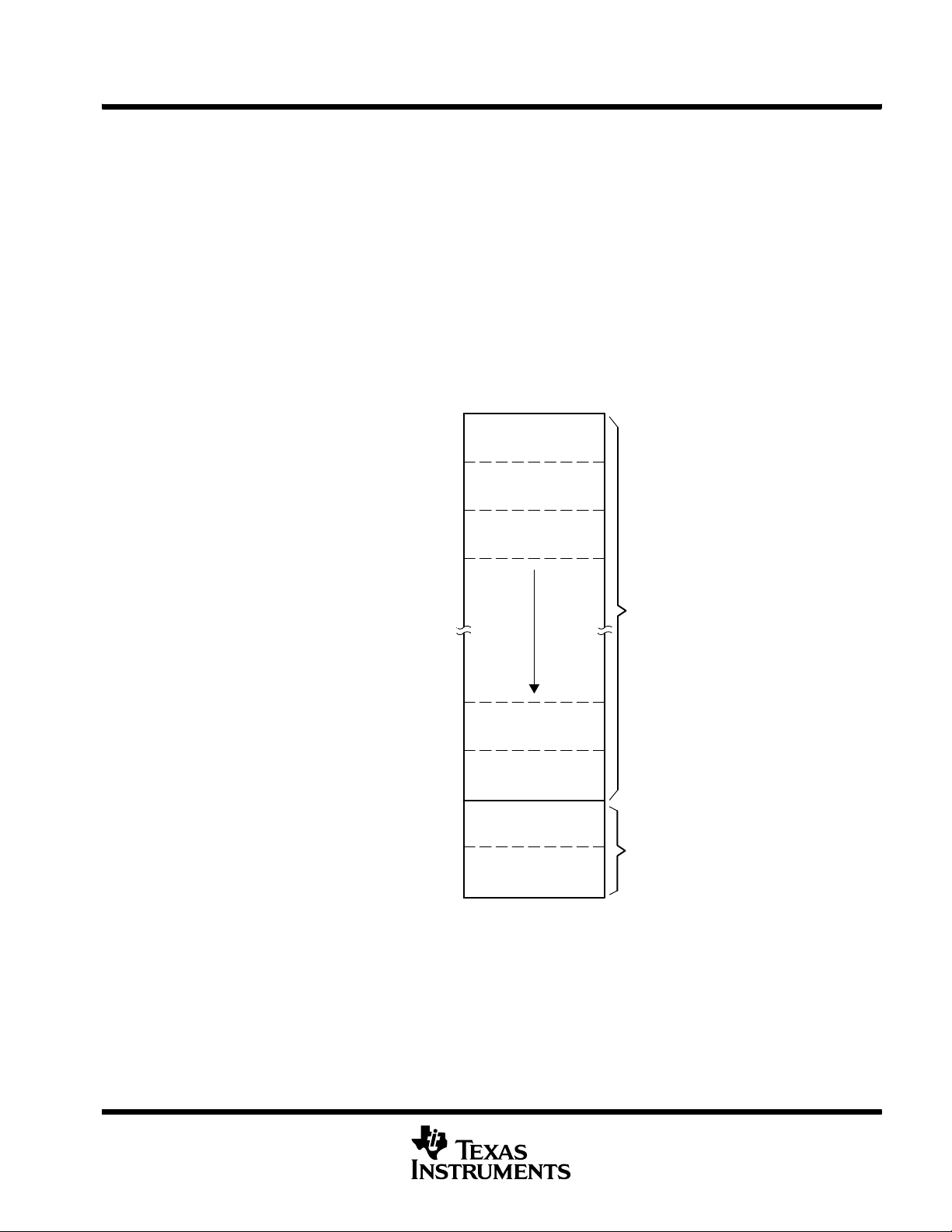
flash memory
The flash memory can be programmed via the JTAG port, the bootstrap loader, or in-system by the CPU. The
CPU c an perform single-byteand single-wordwrites tothe flash memory.Features ofthe flash memory include:
D Flash memory has n segments of main memory and two segments of information memory (A and B) of
128 bytes each. Each segment in main memory is 512 bytes in size.
D Segments 0 to n may be erased in one step, or each segment may be individually erased.
D Segments A and B can be erased individually, or as a group with segments 0 to n.
Segments A and B are also called information memory.
D New devices may have some bytes programmed in the information memory (needed for test during
manufacturing). The user should perform an erase of the information memory prior to the first use.
8KB
0FFFFh
0FE00h
0FDFFh
0FC00h
0FBFFh
0FA00h
0F9FFh
0E400h
0E3FFh
0E200h
0E1FFh
0E000h
010FFh
01080h
0107Fh
01000h
16KB
0FFFFh
0FE00h
0FDFFh
0FC00h
0FBFFh
0FA00h
0F9FFh
0C400h
0C3FFh
0C200h
0C1FFh
0C000h
010FFh
01080h
0107Fh
01000h
B
32
0FFFFh
0FE00h
0FDFFh
0FC00h
0FBFFh
0FA00h
0F9FFh
08400h
083FFh
08200h
081FFh
08000h
010FFh
01080h
0107Fh
01000h
Segment 0
With Interrupt Vectors
Segment 1
Segment 2
Main Memory
Segment n--1
Segment n
Segment A
Information Memory
Segment B
POST OFFICE BOX 655303 • DALLAS, TEXAS 75265
11
Page 12

MSP430F42xA
MIXED SIGNAL MICROCONTROLLER
SLAS587 -- FEBRUARY 2008
peripherals
Peripherals are connected to the CPU through data, address, and control buses and can be handled using all
instructions. For complete module descriptions, see the MSP430x4xx Family User’s Guide, literature number
SLAU056.
oscillator and system clock
The clock system in the MSP430F42xA family of devices is supported by the FLL+ module, which includes
support for a 32768-Hz watch crystal oscillator, an internal digitally-controlled oscillator (DCO), and a
high-frequency crystal oscillator. The FLL+ clock module is designed to meet the requirements of both low
system cost and low power consumption. The FLL+ features digital frequency locked loop (FLL) hardware that,
in conjunction with a digital modulator, stabilizes the DCO frequency to a programmable multiple of the watch
crystal frequency. The internal DCO provides a fast turn-on clock source and stabilizes in less than 6 μs. The
FLL+ module provides the following clock signals:
D Auxiliary clock (ACLK), sourced from a 32768-Hz watch crystal or a high-frequency crystal.
D Main clock (MCLK), the system clock used by the CPU.
D Sub-Main clock (SMCLK), the subsystem clock used by the peripheral modules.
D ACLK/n, the buffered output of ACLK, ACLK/2, ACLK/4, or ACLK/8.
brownout, supply voltage supervisor (SVS)
The brownout circuit is implemented to provide the proper internal reset signal to the device during power on
and power off. The SVS circuitry detects if the supply voltage drops below a user-selectable level and supports
both supply-voltage supervision (the device is automatically reset) and supply-voltage monitoring (SVM) (the
device is not automatically reset).
The CPU begins code execution after the brownout circuit releases the device reset. However, V
have ramped to V
reaches V
CC(min)
CC(min)
. If desired, the SVS circuit can be used to determine when VCCreaches V
at that time. The user must ensure the default FLL+ settings are not changed until V
CC(min)
digital I/O
There are two 8-bit I/O ports implemented—ports P1 and P2 (only six P2 I/O signals are available on external
pins):
D All individual I/O bits are independently programmable.
D Any combination of input, output, and interrupt conditions is possible.
D Edge-selectable interrupt input capability for all the eight bits of port P1 and six bits of P2.
D Read/write access to port-control registers is supported by all instructions.
NOTE:
Six bits of port P2 (P2.0 to P2.5) are available on external pins, but all control and data bits for port
P2 are implemented.
Basic Timer1
CC
.
may not
CC
The Basic Timer1 has two independent 8-bit timers that can be cascaded to form a 16-bit timer/counter. Both
timers can be read and written by software. The Basic Timer1 can be used to generate periodic interrupts and
clock for the LCD module.
LCD drive
The LCD driver generates the segment and common signals required to drive an LCD display. The LCD
controller has dedicated data memory to hold segment drive information. Common and segment signals are
generated as defined by the mode. Static, 2-MUX, 3-MUX, and 4-MUX LCDs are supported by this peripheral.
12
POST OFFICE BOX 655303 • DALLAS, TEXAS 75265
Page 13
MSP430F42xA
A
MIXED SIGNAL MICROCONTROLLER
SLAS587 -- FEBRUARY 2008
watchdog timer (WDT+)
The primary function of the WDT+ module is to perform a controlled system restart after a software problem
occurs. If the selected time interval expires, a system reset is generated. If the watchdog function is not needed
in anapplication, the module can be configured asan interval timer and can generate interruptsat selected time
intervals.
Timer_A3
Timer_A3 is a 16-bit timer/counter with three capture/compare registers. Timer_A3 can support multiple
capture/compares, PWM outputs, and interval timing. Timer_A3 also has extensive interrupt capabilities.
Interrupts may be generated from the counter on overflow conditions and from each of the capture/compare
registers.
TIMER_A3 SIGNAL CONNECTIONS
INPUT PIN
NUMBER
48 - P1.5 TACL K TACLK
48 - P1.5 TACLK INCLK
53 - P1.0 TA0 CCI0A
52 - P1.1 TA0 CCI0B
51 - P1.2 TA1 CCI1A
51 - P1.2 TA1 CCI1B
45 - P2.0 TA2 CCI2A
DEVICE INPUT
SIGNAL
ACLK ACLK
SMCLK SMCLK
DV
SS
DV
CC
DV
SS
DV
CC
ACLK (internal) CCI2B
DV
SS
DV
CC
MODULE INPUT
NAME
GND
V
CC
GND
V
CC
GND
V
CC
MODULE BLOCK
Timer N
CCR0 TA0
CCR1 TA1
CCR2 TA2
MODULE OUTPUT
SIGNAL
OUTPUT PIN
NUMBER
53 - P1.0
51 - P1.2
45 - P2.0
universal synchronous/asynchronous receive transmit (USART)
The MSP430F42xA devices have one hardware USART peripheral module (USART0) that is used for serial
data communication. The USART supports synchronous SPI (3 or 4 pin) and asynchronous UART
communication protocols, using double-buffered transmit and receive channels.
hardware multiplier
The multiplication operation is supported by a dedicated peripheral module. The module performs 16×16,
16×8, 8×16, and 8×8 bit operations. The module is capable of supporting signed and unsigned multiplication,
as well as signed and unsigned multiply and accumulateoperations. Theresult of an operation can be accessed
immediately after the operands have been loaded into the peripheral registers. No additional clock cycles are
required.
SD16
The SD16 moduleintegrates three independent16-bit sigma-delta A/Dconverters, internal temperaturesensor,
and built-in voltage reference. Each channel is designed with a fully differential analog input pair and
programmable gain amplifier input stage.
POST OFFICE BOX 655303 • DALLAS, TEXAS 75265
13
Page 14

MSP430F42xA
_
p
MIXED SIGNAL MICROCONTROLLER
SLAS587 -- FEBRUARY 2008
peripheral file map
PERIPHERALS WITH WORD ACCESS
Watchdog Watchdog timer control WDTCTL 0120h
Timer_A3
Hardware Multiplier
Flash
SD16
(see also: Peripherals
with ByteAccess)
Timer_A interrupt vector TAI V 012Eh
Timer_A control TAC TL 0160h
Capture/compare control 0 TACCTL0 0162h
Capture/compare control 1 TACCTL1 0164h
Capture/compare control 2 TACCTL2 0166h
Timer_A register TAR 0170h
Capture/compare register 0 TACCR0 0172h
Capture/compare register 1 TACCR1 0174h
Capture/compare register 2 TACCR2 0176h
Sum extend SUMEXT 013Eh
Result high word RESHI 013Ch
Result low word RESLO 013Ah
Second operand OP2 0138h
Multiply signed + accumulate/operand1 MACS 0136h
Multiply + accumulate/operand1 MAC 0134h
Multiply signed/operand1 MPYS 0132h
Multiply unsigned/operand1 MPY 0130h
Flash control 3 FCTL3 012Ch
Flash control 2 FCTL2 012Ah
Flash control 1 FCTL1 0128h
General control SD16CTL 0100h
Channel 0 control SD16CCTL0 0102h
Channel 1 control SD16CCTL1 0104h
Channel 2 control SD16CCTL2 0106h
Reserved 0108h
Reserved 010Ah
Reserved 010Ch
Reserved 010Eh
Interrupt vector word register SD16IV 0110h
Channel 0 conversion memory SD16MEM0 0112h
Channel 1 conversion memory SD16MEM1 0114h
Channel 2 conversion memory SD16MEM2 0116h
Reserved 0118h
Reserved 011Ah
Reserved 011Ch
Reserved 011Eh
14
POST OFFICE BOX 655303 • DALLAS, TEXAS 75265
Page 15

peripheral file map (continued)
SD16
(see also: Peripherals
with WordAccess)
LCD
USART0
Brownout, SVS SVS control register SVSCTL 056h
FLL+ Clock
Basic Timer1
MSP430F42xA
MIXED SIGNAL MICROCONTROLLER
SLAS587 -- FEBRUARY 2008
PERIPHERALS WITH BYTE ACCESS
Channel 0 input control SD16INCTL0 0B0h
Channel 1 input control SD16INCTL1 0B1h
Channel 2 input control SD16INCTL2 0B2h
Reserved 0B3h
Reserved 0B4h
Reserved 0B5h
Reserved 0B6h
Reserved 0B7h
Channel 0 preload SD16PRE0 0B8h
Channel 1 preload SD16PRE1 0B9h
Channel 2 preload SD16PRE2 0BAh
Reserved 0BBh
Reserved 0BCh
Reserved 0BDh
Reserved 0BEh
Reserved 0BFh
LCD memory 20 LCDM20 0A4h
: : :
LCD memory 16 LCDM16 0A0h
LCD memory 15 LCDM15 09Fh
: : :
LCD memory 1 LCDM1 091h
LCD control and mode LCDCTL 090h
Transmit buffer U0TXBUF 077h
Receive buffer U0RXBUF 076h
Baud rate U0BR1 075h
Baud rate U0BR0 074h
Modulation control U0MCTL 073h
Receive control U0RCTL 072h
Transmit control U0TCTL 071h
USART control U0CTL 070h
FLL+ control 1 FLL_CTL1 054h
FLL+ control 0 FLL_CTL0 053h
System clock frequency control SCFQCTL 052h
System clock frequency integrator SCFI1 051h
System clock frequency integrator SCFI0 050h
BT counter 2 BTCNT2 047h
BT counter 1 BTCNT1 046h
BT control BTCTL 040h
POST OFFICE BOX 655303 • DALLAS, TEXAS 75265
15
Page 16

MSP430F42xA
p
MIXED SIGNAL MICROCONTROLLER
SLAS587 -- FEBRUARY 2008
peripheral file map (continued)
PERIPHERALS WITH BYTE ACCESS (CONTINUED)
Port P2
Port P1
Special Functions
Port P2 selection P2SEL 02Eh
Port P2 interrupt enable P2IE 02Dh
Port P2 interrupt-edge select P2IES 02Ch
Port P2 interrupt flag P2IFG 02Bh
Port P2 direction P2DIR 02Ah
Port P2 output P2OUT 029h
Port P2 input P2IN 028h
Port P1 selection P1SEL 026h
Port P1 interrupt enable P1IE 025h
Port P1 interrupt-edge select P1IES 024h
Port P1 interrupt flag P1IFG 023h
Port P1 direction P1DIR 022h
Port P1 output P1OUT 021h
Port P1 input P1IN 020h
SFR module enable 2 ME2 005h
SFR module enable 1 ME1 004h
SFR interrupt flag 2 IFG2 003h
SFR interrupt flag 1 IFG1 002h
SFR interrupt enable 2 IE2 001h
SFR interrupt enable 1 IE1 000h
16
POST OFFICE BOX 655303 • DALLAS, TEXAS 75265
Page 17

MSP430F42xA
(LFXT1)
LFXT1crystalfrequency,f
(LFXT1)
(seeNote3
)
f
MIXED SIGNAL MICROCONTROLLER
SLAS587 -- FEBRUARY 2008
absolute maximum ratings
Voltage applied at VCCto V
Voltage applied to any pin (see Note 1) --0.3 V to V
†
SS
--0.3 V to + 4.1 V....................................................
+0.3V.......................................
CC
Diode current at any device terminal . ±2mA......................................................
Storage temperature (unprogrammed device) --55°C to 150°C......................................
Storage temperature (programmed device) --40°Cto85°C.........................................
†
Stresses beyond those listed under “absolute maximum ratings” may cause permanent damage to the device. These are stress ratingsonly,and
functional operation of the device at these or any other conditions beyond those indicated under “recommended operating conditions” is not
implied. Exposure to absolute-maximum-rated conditions for extended periods may affect device reliability.
NOTE 1: All voltages referenced to V
applied to the TDI/TCLK pin when blowing the JTAG fuse.
. The JTAG fuse-blow voltage, VFB, is allowed to exceed the absolute maximum rating. The voltage is
SS
recommended operating conditions
PARAMETER MIN NOM MAX UNITS
Supply voltage during program execution, SD16 disabled,
V
(AVCC=DVCC=VCC)(seeNote1)
CC
Supply voltage during program execution, SD16 disabled, SVS enabled, and
PORON = 1, V
Supply voltage during program execution, SD16 enabled or
during programming of flash memory, V
Supply voltage, VSS(AVSS=DVSS=VSS) 0 0 V
Operating free-air temperature range, T
LFXT1 crystal frequency, f
Processorfrequency (signal MCLK),
NOTES: 1. It is recommended to power AVCCand DVCCfrom the same source. A maximum difference of 0.3 V between AVCCand DVCCcan
2. The minimumoperatingsupply voltage is defined according tothe trip point where PORis going active by decreasingsupply voltage.
3. The LFXT1 oscillator in LF-mode requires a watch crystal.
(AVCC=DVCC=VCC) (see Notes 1 and 2)
CC
(AVCC=DVCC=VCC)
CC
A
LF selected, XTS_FLL = 0 Watch crystal 32768 Hz
(see Note 3)
(System)
be tolerated during power up and operation.
POR is going inactive when the supply voltage is raised above minimum supply voltage plus the hysteresis of the SVS circuitry.
XT1 selected, XTS_FLL = 1 Ceramic resonator 450 8000 kHz
XT1 selected, XTS_FLL = 1 Crystal 1000 8000 kHz
MSP430F42xA 1.8 3.6 V
MSP430F42xA 2.0 3.6 V
MSP430F42xA 2.7 3.6 V
MSP430F42xA -- 4 0 85 °C
VCC=1.8V DC 4.15
VCC=3.6V DC 8
MHz
f(MHz)
4.15 MHz
-- Maximum Processor Frequency -- MHz
System
f
Supply Voltage Range With SD16
Enabled or During Programming
8MHz
6MHz
of the Flash Memory
Supply Voltage Range
During Program
Execution
1.8 V 3.6 V
VCC-- Supply Voltage -- V
2.7V 3V
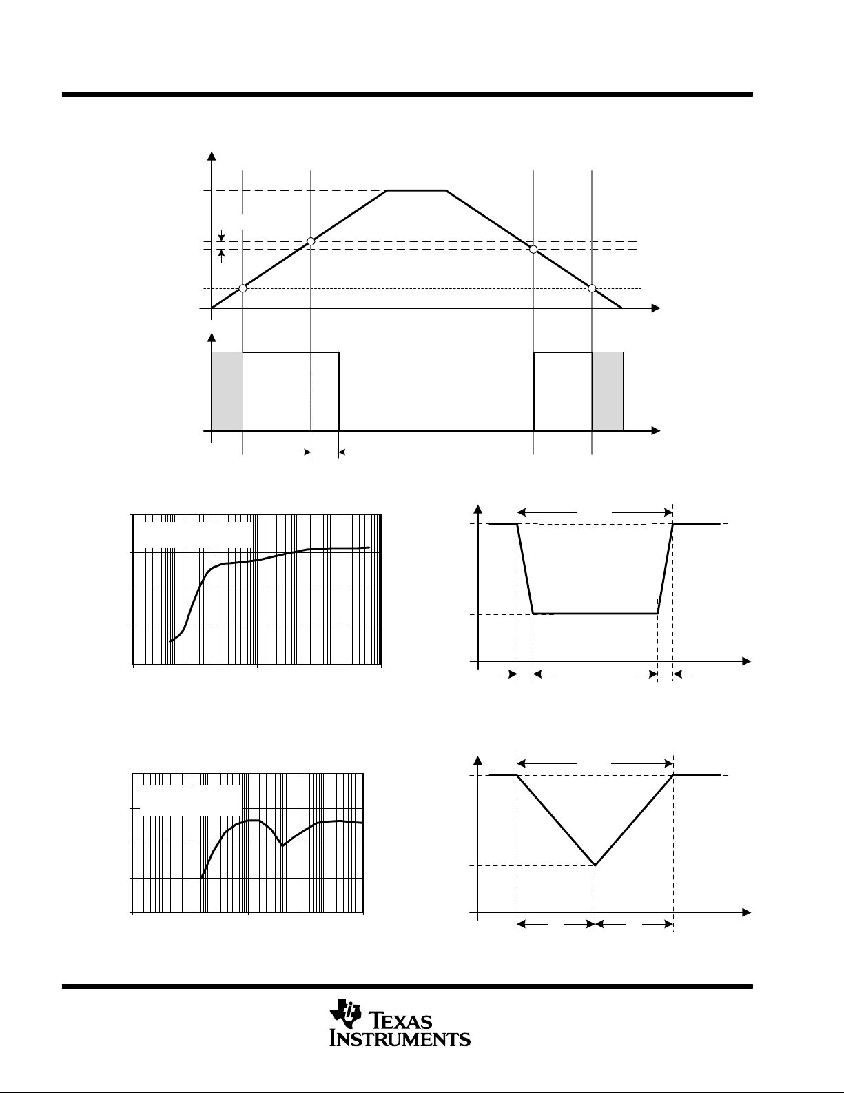
Figure 1. Frequency vs Supply Voltage
POST OFFICE BOX 655303 • DALLAS, TEXAS 75265
17
Page 18
MSP430F42xA
V
A
(
)
I
(LPM4
)
Lowpowermode,(LPM4)(seeNote2)
3
V
μ
A
MIXED SIGNAL MICROCONTROLLER
SLAS587 -- FEBRUARY 2008
electrical characteristics over recommended operating free-air temperature (unless otherwise
noted)
supply current into AVCC+DVCCexcluding external current (see Note 1)
PARAMETER TEST CONDITIONS V
Active mode,
f
I
(AM)
I
(LPM0)
I
(LPM2)
I
(LPM3)
I
LPM4
NOTES: 1. All inputs are tied to 0 V or VCC. Outputs do not source or sink any current.
(MCLK)=f(SMCLK)=f(DCO)
f
= 32,768 Hz, XTS_FLL = 0
(ACLK)
(program executes in flash)
Low-power mode, (LPM0/LPM1)
f
(MCLK)=f(SMCLK)=f(DCO)
f
= 32,768 Hz, XTS_FLL = 0
(ACLK)
FN_8=FN_4=FN_3=FN_2=0(seeNote2)
Low-power mode, (LPM2) (see Note 2) TA=--40°Cto85°C 3V 10 22 μA
Low-power mode, (LPM3) (see Note 2)
Low-power mode, (LPM4) (see Note 2)
The current consumption in LPM2, LPM3, and LPM4 are measured with active Basic Timer1 and LCD (ACLK selected).
The current consumption of the SD16 and the SVS module are specified in their respective sections.
LPMx currents measured with WDT disabled.
The currents are characterized with a KDSDaishinkuDT--38(6pF)crystal.
2. Current for brownout included.
=1MHz,
=1MHz,
TA=--40°Cto85°C 3V 400 500 μA
TA=--40°Cto85°C 3V 130 150 μA
TA=--40°C 1.5 2.0
TA=25°C
T
=60°C
A
TA=85°C 2.0 3.5
TA=--40°C 0.1 0.5
T
=25°C
A
TA=85°C
CC
3
3V
MIN TYP MAX UNIT
1.6 2.1
1.7 2.2
0.1 0.5
0.8 2.5
μ
μA
current consumption of active mode versus system frequency
I
(AM)=I(AM) [1 MHz]
× f
(System) [MHz]
current consumption of active mode versus supply voltage
I
(AM)=I(AM) [3 V]
+ 170 μA/V × (VCC–3V)
18
POST OFFICE BOX 655303 • DALLAS, TEXAS 75265
Page 19

MSP430F42xA
g
g
PortP
1,P2:P1.xtoP2.x,Externaltriggersignal
Leakage
V
A
V
V
V
V
C
2
0pF
Xdc
frequency
MIXED SIGNAL MICROCONTROLLER
SLAS587 -- FEBRUARY 2008
electrical characteristics over recommended operating free-air temperature (unless otherwise
noted) (continued)
Schmitt-trigger inputs -- Ports P1 and P2, RST/NMI, JTAG (TCK, TMS, TDI/TCLK, TDO/TDI)
PARAMETER V
V
IT+
V
IT--
V
hys
Positive-going input threshold voltage 3V 1.5 1.98 V
Negative-going input threshold voltage 3V 0.9 1.3 V
Input voltage hysteresis (V
IT+
-- V
) 3V 0.45 1 V
IT--
inputs Px.x, TAx
PARAMETER TEST CONDITIONS V
t
(int)
t
(cap)
f
(TAext)
f
(TAint)
External interrupt timing
Timer_A, capture timing TA x 3V 50 ns
Timer_A clock frequency
externally applied to pin
Timer_A clock frequency SMCLK or ACLK signal selected 3V 10 MHz
NOTES: 1. The external signal sets the interrupt flag every time the minimum t
trigger signals s horter than t
MCLK cycles.
Port P1, P2: P1.xto P2.x,External tri
for the interrupt flag, (see Note 1)
TACLK, INCLK t
. Both the cycle and timing specifications must be met to ensure the flag is set. t
(int)
(H)=t(L)
CC
CC
er signal
3V 1.5 cycle
3V 50 ns
3V 10 MHz
cycle and time parameters are met. It may be set even with
(int)
MIN TYP MAX UNIT
MIN TYP MAX UNIT
is measured in
(int)
leakage current (see Note 1)
I
lkg(P1.x)
I
lkg(P2.x)
PARAMETER TEST CONDITIONS V
Leakage current
Port P1 Port 1: V
Port P2 Port 2: V
(P1.x)
(P2.x)
(see Note 2)
(see Note 2)
CC
3
NOTES: 1. The leakage current is measured with VSSor VCCapplied to the corresponding pin(s), unless otherwise noted.
2. The port pin must be selected as an input.
MIN NOM MAX UNIT
outputs -- Ports P1 and P2
PARAMETER TEST CONDITIONS V
V
V
High-level output voltage
OH
Low-level output voltage
OL
NOTES: 1. The maximum total current, I
maximum specified voltage drop.
2. The maximum total current, I
maximum specified voltage drop.
I
OH(max) =
I
OH(max) =
I
OL(max) =
I
OL(max) =
OH(max)
OH(max)
--1.5mA(seeNote1)
--6mA(seeNote2)
1.5mA(seeNote1)
6mA(seeNote2)
and I
and I
for all outputs combined, should not exceed ±12 mA to satisfy the
OL(max),
for all outputs combined, should not exceed ±48 mA to satisfy the
OL(max),
CC
3
3
MIN TYP MAX UNIT
VCC--0.25 V
VCC-- 0 . 6 V
V
SS
V
SS
VSS+0.25
output frequency
f
Px.y
f
ACLK,
f
MCLK,
f
SMCLK
t
Xdc
PARAMETER TEST CONDITIONS V
CC
(1 ≤ x ≤ 2, 0 ≤ y ≤ 7) CL=20pF,IL= ± 1.5 mA 3V dc 12 MHz
P1.1/TA0/MCLK
P1.5/TACLK/ACLK/S28
Duty cycle ofoutput
CL=20pF 3V 12 MHz
f
P1.5/TACLK/ACLK/S28,
=
L
P1.1/TA0/MCLK, CL=20pF,f
ACLK=fLFXT1=fXT1
f
ACLK=fLFXT1=fLF
f
ACLK=fLFXT1
MCLK=fDCOCLK
3V
MIN TYP MAX UNIT
40% 60%
30% 70%
50%
50%-15 ns
50%
±50
±50
CC
CC
VSS+0.6
50%+
15 ns
n
POST OFFICE BOX 655303 • DALLAS, TEXAS 75265
19
Page 20

MSP430F42xA
A
MIXED SIGNAL MICROCONTROLLER
SLAS587 -- FEBRUARY 2008
electrical characteristics over recommended operating free-air temperature (unless otherwise
noted) (continued)
outputs -- Ports P1 and P2 (continued)
TYPICAL LOW-LEVEL OUTPUT CURRENT
vs
LOW-LEVEL OUTPUT VOLTAGE
30
VCC=2.2V
P2.1
25
20
15
10
5
-- Typical Low-Level Output Current -- mA
OL
I
0
0.0 0.5 1.0 1.5 2.0 2.5
VOL-- Low-Level Output Voltage -- V
TA=25°C
TA=85°C
Figure 2
TYPICAL LOW-LEVEL OUTPUT CURRENT
vs
LOW-LEVEL OUTPUT VOLTAGE
50
VCC=3V
P2.1
40
30
20
10
-- Typical Low-Level Output Current -- mA
OL
I
0
0.0 0.5 1.0 1.5 2.0 2.5 3.0 3.5
VOL-- Low-Level Output Voltage -- V
TA=25°C
TA=85°C
Figure 3
TYPICAL HIGH-LEVEL OUTPUT CURRENT
HIGH-LEVEL OUTPUT VOLTAGE
0
VCC=2.2V
P2.1
-- 5
-- 1 0
-- 1 5
-- 2 0
TA=85°C
-- 2 5
-- Typical High-Level Output Current -- m
OL
I
-- 3 0
0.0 0.5 1.0 1.5 2.0 2.5
VOH-- High-Level Output Voltage -- V
TA=25°C
Figure 4
NOTE: One output loaded at a time
vs
TYPICAL HIGH-LEVEL OUTPUT CURRENT
vs
HIGH-LEVEL OUTPUT VOLTAGE
0
VCC=3V
P2.1
-- 1 0
-- 2 0
-- 3 0
TA=85°C
-- 4 0
-- Typical High-Level Output Current -- mA
OL
I
-- 5 0
0.0 0.5 1.0 1.5 2.0 2.5 3.0 3.5
VOH-- High-Level Output Voltage -- V
TA=25°C
Figure 5
20
POST OFFICE BOX 655303 • DALLAS, TEXAS 75265
Page 21
MSP430F42xA
)
t
d(LPM3)
Delaytime
3
V
μ
s
A
V
V
V
p
g
l
i
Segmentline
V
V
V
B
MIXED SIGNAL MICROCONTROLLER
SLAS587 -- FEBRUARY 2008
electrical characteristics over recommended operating free-air temperature (unless otherwise
noted) (continued)
wake-up LPM3
PARAMETER TEST CONDITIONS V
CC
f=1MHz 6
t
d(LPM3
Delay time
f=2MHz
3V
f=3MHz
RAM (see Note 1)
PARAMETER TEST CONDITIONS MIN TYP MAX UNIT
VRAMh CPUhalted(seeNote1) 1.6 V
NOTE 1: This parameter defines the minimum supply voltage when the data in the program memory RAM remain unchanged. No program
execution should take place during this supply voltage condition.
LCD
PARAMETER TEST CONDITIONS MIN TYP MAX UNIT
V
(33)
V
(23)
V
(13)
V
(33) --V(03)
I
(R03)
I
(R13)
I
(R23)
V
(Sxx0)
V
(Sxx1)
V
(Sxx2)
V
(Sxx3)
nalog voltage
Input leakage
Segment line
voltage
Voltage at R33 2.5 VCC+0.2
Voltage at R23
Voltage at R13
CC
=3
(V33-- V03) × 2/3 + V
(V
-- V
(33)
Voltage at R33/R03 2.5 VCC+0.2
R03 = V
SS
R13 = VCC/3
R23 = 2 × VCC/3
I
=--3μA,
(Sxx)
No load at all
segment and
common
V
CC
CC
nes,
=3V
=3
V(
V(
V
(03)
V
(13)
23)
33)
MIN TYP MAX UNIT
03
) × 1/3 + V
(03)
(03)
±20
±20
±20
V
(03)
V
(13)
V
(23)
V
(33)
-- 0 . 1
-- 0 . 1
-- 0 . 1
+0.1
6
μs
6
nA
USART0 (see Note 1)
PARAMETER TEST CONDITIONS MIN TYP MAX UNIT
t
(τ)
NOTE 1: The signal applied to theUSART0 receive signal/terminal (URXD0) should meet the timing requirements of t
USART0: deglitch time VCC= 3 V, SYNC = 0, UART mode 150 280 500 ns
to ensure that the URXS
(τ
flip-flop is set. The URXS flip-flop is set with negative pulses meeting the minimum-timing condition of t
)
. The operating conditions to
(τ
)
set the flag must be met independently from this timing constraint. The deglitch circuitry is active only on negative transitions on the
URXD0 line.
POR brownout, reset (see Notes 1 and 2)
PARAMETER TEST CONDITIONS MIN TYP MAX UNIT
t
d(BOR)
V
CC(start)
V
(B_IT--)
V
hys(B_IT--)
t
(reset)
rownout
dVCC/dt ≤ 3 V/s (see Figure 6) 0.7 × V
dVCC/dt ≤ 3 V/s (see Figure 6, Figure 7, and Figure 8) 1.71 V
dVCC/dt ≤ 3 V/s (see Figure 6) 70 130 180 mV
Pulse length needed at RST/NMI pin to accepted reset i nternally,
V
=3V
CC
2 μs
NOTES: 1. The current consumption of the brownout module is already included in the ICCcurrent consumption data. The voltage level
V
(B_IT--)+Vhys(B_IT--)
2. During power up, the CPU begins code execution following a period of t
The default FLL+ settings must not be changed until V
is ≤ 1.8 V.
CC
≥ V
CC(min)
d(BOR)
, where V
after VCC=V
is the minimum supply voltage for the desired
CC(min)
(B_IT--)+Vhys(B_IT--)
operating frequency. See the MSP430x4xx Family User’s Guide (SLAU056) for more information on the brownout/SVS circuit.
2000 μs
(B_IT--)
.
V
POST OFFICE BOX 655303 • DALLAS, TEXAS 75265
21
Page 22
MSP430F42xA
MIXED SIGNAL MICROCONTROLLER
SLAS587 -- FEBRUARY 2008
electrical characteristics over recommended operating free-air temperature (unless otherwise
noted) (continued)
V
CC
V
hys(B_IT--)
V
(B_IT--)
V
CC(start)
1
0
t
d(BOR)
Figure 6. POR/Brownout Reset (BOR) vs Supply Voltage
2
V=3V
cc
Typical Conditions
1.5
1
(drop) -- V
CC
V
0.5
0
0.001 1 1000
tpw-- Pulse Width -- μst
Figure 7. V
2
V=3V
Typical Conditions
1.5
1
(drop) -- V
CC
0.5
V
0
0.001 1 1000
CC(drop)
cc
tpw-- Pulse Width -- μs
Level With a Square Voltage Drop to Generate a POR/Brownout Signal
V
CC(drop)
V
CC(drop)
V
3V
V
3V
CC
CC
t
pw
1ns 1ns
-- Pulse Width -- μs
pw
t
pw
tf=t
r
t
f
tpw-- Pulse Width -- μs
t
r
22
Figure 8. V
CC(drop)
Level With a Triangle Voltage Drop to Generate a POR/Brownout Signal
POST OFFICE BOX 655303 • DALLAS, TEXAS 75265
Page 23
MSP430F42xA
)
V
hys(SVS_I
T--)
/
V
V
MIXED SIGNAL MICROCONTROLLER
SLAS587 -- FEBRUARY 2008
electrical characteristics over recommended operating free-air temperature (unless otherwise
noted) (continued)
SVS (supply voltage supervisor/monitor) (see Note 1)
PARAMETER TEST CONDITIONS MIN TYP MAX UNIT
t
(SVSR)4
t
d(SVSon)
t
settle
V
(SVSstart)
V
hys(SVSIT--
(SVS_IT--)
I
CC(SVS)
(see Note 1)
†
The recommended operating voltage range is limited to 3.6 V.
‡
t
is the settling time that the comparator o/p needs to have a stable level after VLD is switched VLD ≠ 0 to a different VLD value somewhere
settle
between 2 and 15. The overdrive is assumed to be > 50 mV.
NOTE 1: The current consumption of the SVS module is not included in the I
dVCC/dt > 30 V/ms (see Figure 9) 5 150
dVCC/dt ≤ 30 V/ms 2000
μs
SVSon, switch from VLD = 0 to VLD ≠ 0, VCC=3V 20 150 μs
‡
VLD ≠ 0
12 μs
VLD ≠ 0, VCC/dt ≤ 3 V/s (see Figure 9) 1.55 1.7 V
VLD = 1 70 120 155 mV
VCC/dt ≤ 3 V/s (see Figure 9)
VCC/dt ≤ 3 V/s (see Figure 9),
External voltage applied on P2.3
VLD=2to14
VLD = 15 1 20 mV
V
(SVS_IT--)
x 0.001
V
(SVS_IT--)
x 0.016
VLD = 1 1.8 1.9 2.05
VLD = 2 1.94 2.1 2.25
VLD = 3 2.05 2.2 2.37
VLD = 4 2.14 2.3 2.48
VLD = 5 2.24 2.4 2.6
VLD = 6 2.33 2.5 2.71
V
dt ≤ 3V/s(seeFigure9)
CC
VLD = 7 2.46 2.65 2.86
VLD = 8 2.58 2.8 3
VLD = 9 2.69 2.9 3.13
VLD = 10 2.83 3.05 3.29
VLD = 11 2.94 3.2 3.42
3.99
†
†
†
VCC/dt ≤ 3 V/s (see Figure 9),
External voltage applied on P2.3
VLD = 12 3.11 3.35 3.61
VLD = 13 3.24 3.5 3.76
VLD = 14 3.43 3.7
†
VLD = 15 1.1 1.2 1.3
VLD ≠ 0, VCC=2.2V/3V 10 15 μA
current consumption data.
CC
POST OFFICE BOX 655303 • DALLAS, TEXAS 75265
23
Page 24

MSP430F42xA
MIXED SIGNAL MICROCONTROLLER
SLAS587 -- FEBRUARY 2008
electrical characteristics over recommended operating free-air temperature (unless otherwise
noted) (continued)
Software Sets VLD>0:
V
V
(SVS_IT--)
V
(SVSstart)
V
(B_IT--)
V
CC(start)
CC
V
V
hys(B_IT--)
hys(SVS_IT--)
SVS is Active
Brownout
SVS out
Set POR
1.5
-- V
CC(drop)
V
0.5
Brownout
Region
1
0
t
d(BOR)
1
0
t
1
Undefined
0
Figure 9. SVS Reset (SVSR) vs Supply Voltage
2
Rectangular Drop
Triangular Drop
1
0
1 10 1000
-- Pulse Width -- μs
t
pw
100
SVS Circuit is Active From VLD > to VCC<V
d(SVSon)
V
CC
3V
V
CC(drop)
1ns 1ns
V
CC
3V
(B_IT-- )
t
d(SVSR)
Brownout
Region
t
d(BOR)
t
pw
t
pw
Figure 10. V
24
CC(drop)
V
CC(drop)
tf=t
r
t
f
t
r
t -- Pulse Width -- μs
With a Square Voltage Drop and a Triangle Voltage Drop to Generate an SVS Signal
POST OFFICE BOX 655303 • DALLAS, TEXAS 75265
Page 25

MSP430F42xA
f
/
f
MIXED SIGNAL MICROCONTROLLER
SLAS587 -- FEBRUARY 2008
electrical characteristics over recommended operating free-air temperature (unless otherwise
noted) (continued)
DCO
PARAMETER TEST CONDITIONS V
f
(DCOCLK)
f
(DCO = 2)
f
(DCO = 27)
f
(DCO = 2)
f
(DCO = 27)
f
(DCO = 2)
f
(DCO = 27)
f
(DCO = 2)
f
(DCO = 27)
f
(DCO = 2)
f
(DCO = 27)
S
n
D
t
D
V
N
f
FN_8 = FN_4 = FN_3 = FN_2 = 0, DCOPLUS = 1 3V 0.3 0.7 1.3 MHz
FN_8 = FN_4 = FN_3 = FN_2 = 0, DCOPLUS = 1 3V 2.7 6.1 11 .3 MHz
FN_8 = FN_4 = FN_3 = 0, FN_2 = 1, DCOPLUS = 1 3V 0.8 1.5 2.5 MHz
FN_8 = FN_4 = FN_3 = 0, FN_2 = 1, DCOPLUS = 1 3V 6.5 12.1 20 MHz
FN_8 = FN_4 = 0, FN_3 = 1, FN_2 = x, DCOPLUS = 1 3V 1.3 2.2 3.5 MHz
FN_8 = FN_4 = 0, FN_3 = 1, FN_2 = x, DCOPLUS = 1 3V 10.3 17.9 28.5 MHz
FN_8 = 0, FN_4 = 1, FN_3 = FN_2 = x, DCOPLUS = 1 3V 2.1 3.4 5.2 MHz
FN_8 = 0, FN_4 = 1, FN_3 = FN_2 = x, DCOPLUS = 1 3V 16 26.6 41 MHz
FN_8 = 1, FN_4 = FN_3 = FN_2 = x, DCOPLUS = 1 3V 4.2 6.3 9.2 MHz
FN_8 = 1, FN_4 = FN_3 = FN_2 = x, DCOPLUS = 1 3V 30 46 70 MHz
Step size between adjacent DCO taps:
Sn=
(see Figure 12 for taps 21 to 27)
Temperature drift, N
D = 2, DCOPLUS = 0
Drift with VCCvariation, N
D = 2, DCOPLUS = 0
01Eh, FN_8 = FN_4 = FN_3 = FN_2 = 0, D = 2, DCOPLUS = 0,
(DCO) =
= 32.768 kHz
Crystal
DCO(Tap n+1)
DCO(Tap n)
= 01Eh, FN_8 = FN_4 = FN_3 = FN_2 = 0,
(DCO)
= 01Eh, FN_8 = FN_4 = FN_3 = FN_2 = 0,
(DCO)
1<TAP≤ 20 1.06 1.11
TAP = 27 1.07 1.17
CC
3V 1 MHz
3V –0.2 –0.3 –0.4 %/_C
MIN TYP MAX UNIT
0 5 15 %/V
f
(DCO)
f
(DCO3V)
1.0
f
(DCO)
f
(DCO20°C)
1.0
1.8 3.02.4 3.6
20 6040 85
0-- 2 0-- 4 00
Figure 11. DCO Frequency vs Supply Voltage VCCand vs Ambient Temperature
TA-- °CVCC-- V
POST OFFICE BOX 655303 • DALLAS, TEXAS 75265
25
Page 26

MSP430F42xA
MIXED SIGNAL MICROCONTROLLER
SLAS587 -- FEBRUARY 2008
electrical characteristics over recommended operating free-air temperature (unless otherwise
noted) (continued)
1.17
(DCO)
f
- Stepsize Ratio Between DCO Taps
S
1.11
1.07
n
1.06
Min
12720
DCO Tap
Max
Figure 12. DCO Tap Step Size
Legend
Tolerance at Tap 27
DCO Frequency
Adjusted by Bits
9
2
to 25in SCFI1 {N
Tol era nc e at Tap 2
{DCO}
}
26
FN_2=0
FN_3=0
FN_4=0
FN_8=0
Overlapping DCO Ranges:
Uninterrupted Frequency Range
FN_2=1
FN_3=0
FN_4=0
FN_8=0
FN_2=x
FN_3=1
FN_4=0
FN_8=0
FN_2=x
FN_3=x
FN_4=1
FN_8=0
FN_2=x
FN_3=x
FN_4=x
FN_8=1
Figure 13. Five Overlapping DCO Ranges Controlled by FN_x Bits
POST OFFICE BOX 655303 • DALLAS, TEXAS 75265
Page 27

MSP430F42xA
Integratedinputcapacitanc
e
Integratedoutputcapacitance
V
V
MIXED SIGNAL MICROCONTROLLER
SLAS587 -- FEBRUARY 2008
electrical characteristics over recommended operating free-air temperature (unless otherwise
noted) (continued)
crystal oscillator, LFXT1 oscillator (see Notes 1 and 2)
PARAMETER TEST CONDITIONS V
OSCCAPx = 0h 3V 0
C
XIN
C
XOUT
V
IL
V
IH
NOTES: 1. The parasitic capacitance from the package and board may be estimated to be 2pF. The effective load capacitor for the crystal is
Integrated input capacitance
(see Note 4)
Integrated output capacitance
(see Note 4)
Input levels at XIN seeNote3 3
(C
XINxCXOUT
2. To improve EMI on the low-power LFXT1 oscillator, particularly in the LF mode (32 kHz), the following guidelines must be
observed:
• Keep as short a trace as possible between the ’F42xA and the crystal.
• Design a good ground plane around oscillator pins.
• Prevent crosstalk from other clock or data lines into oscillator pins XIN and XOUT.
• Avoid running PCB traces underneath or adjacent to XIN an XOUT pins.
• Use assembly materials and praxis to avoid any parasitic load on the oscillator XIN and XOUT pins.
• If conformal coating is used, ensure that it does not induce capacitive/resistive leakage between the oscillator pins.
• Do not route the XOUT line to the JTAG header to support the serial programming adapter as shown in other documentation.
This signal is no longer required for the serial programming adapter.
3. Applies only whenusingan external logic-level clock source. XTS_FLLmust be set. Not applicable whenusing a crystal or resonator.
4. External capacitance is recommended for precision real-time clock applications, OSCCAPx = 0h.
)/(C
XIN+CXOUT
). It is independent of XTS_FLL.
OSCCAPx = 1h
OSCCAPx = 2h
OSCCAPx = 3h 3V 18
OSCCAPx = 0h 3V 0
OSCCAPx = 1h
OSCCAPx = 2h
OSCCAPx = 3h 3V 18
CC
3V 10
3V 14
3V 10
3V 14
MIN TYP MAX UNIT
V
0.8×V
SS
CC
0.2×V
V
CC
CC
pF
pF
POST OFFICE BOX 655303 • DALLAS, TEXAS 75265
27
Page 28
MSP430F42xA
SD16L
P=0
f
SD1
6
1MHz,
I
SD1
6ch
l
A
f
f
Differentialinput
Vperformanc
e
(seeNote2
)
MIXED SIGNAL MICROCONTROLLER
SLAS587 -- FEBRUARY 2008
electrical characteristics over recommended operating free-air temperature (unless otherwise
noted) (continued)
SD16, power supply and recommended operating conditions
PARAMETER TEST CONDITIONS V
AV
SD16
CC
Analog supply
voltage
Analog supply
current: 1 active
anne
including internal
reference
AVCC=DVCC,AVSS=DVSS=0V 2.7 3.6 V
=
f
SD16
,
=1MHz,
SD16OSR = 256
SD16LP = 1,
=0.5MHz,
SD16
SD16OSR = 256
SD16
Analog front-end
input clock
frequency
SD16LP = 0 (Low power mode disabled) 3V 1
SD16LP = 1 (Low power mode enabled) 3V 0.5
SD16, analog input range (see Note 1)
PARAMETER TEST CONDITIONS V
SD16GAINx = 1, SD16REFON = 1 ±500
Differential input
voltage range for
V
ID
specified
(see Note 2)
Input impedance
Z
I
(one input pin to
AV
)
SS
Differential input
Z
ID
V
I
V
IC
impedance
(IN+ to IN--)
Absolute input
voltage range
Common-mode
input voltage range
NOTES: 1. All parameters pertain to each SD16 channel.
2. The analog input range depends on the reference voltage applied to V
is defined by V
V
or V
FSR+
FSR--
SD16GAINx = 2, SD16REFON = 1
SD16GAINx = 4, SD16REFON = 1 ±125
SD16GAINx = 8, SD16REFON = 1 ±62
SD16GAINx = 16, SD16REFON = 1
SD16GAINx = 32, SD16REFON = 1 ±15
f
= 1MHz, SD16GAINx = 1 3V 200
SD16
= 1MHz, SD16GAINx = 32 3V 75
f
SD16
f
= 1MHz, SD16GAINx = 1 3V 300 400
SD16
f
= 1MHz, SD16GAINx = 32 3V 100 150
SD16
FSR+
=+(V
/2)/GAIN and V
REF
.
GAIN:1,2 3V 650 950
GAIN:4,8,16 3V 730 1100
GAIN: 32 3V 1050 1550
GAIN: 1 3V 620 930
GAIN: 32 3V 700 1060
FSR--
=--(V
.IfV
/2)/GAIN. The analog input range should not exceed 80% of
REF
REF
is sourced externally, the full-scale range
REF
MIN TYP MAX UNIT
CC
MIN TYP MAX UNIT
CC
±250
±31
AVSS-
1.0V
AVSS-
1.0V
AV
AV
CC
CC
μ
MHz
m
kΩ
kΩ
V
V
28
POST OFFICE BOX 655303 • DALLAS, TEXAS 75265
Page 29

MSP430F42xA
f
Signaltonoise
+
f
I
N
50H
z
f
f
p
p
/
ppm
Commonmod
e
V
Senso
r
l
t
2
)
m
V
MIXED SIGNAL MICROCONTROLLER
SLAS587 -- FEBRUARY 2008
electrical characteristics over recommended operating free-air temperature (unless otherwise
noted) (continued)
SD16, analog performance (f
PARAMETER TEST CONDITIONS V
SINAD
G
E
OS
dE
dT
OS
CMRR
AC PSRR
X
T
Signal-to-noise +
distortion ratio
Nominal gain
O
set error
Offset error
temperature
coefficient
Common-mode
rejection ratio
AC power-supply
rejection ratio
Crosstalk 3V <--100 dB
= 1MHz, SD16OSRx = 256, SD16REFON = 1)
SD16
MIN TYP MAX UNIT
CC
SD16GAINx = 1, Signal Amplitude = 500 mV 3V 83.5 85
SD16GAINx = 2, Signal Amplitude = 250 mV 3V 81.5 84
SD16GAINx = 4, Signal Amplitude = 125 mV
SD16GAINx = 8, Signal Amplitude = 62 mV
=
=
100Hz
50Hz,
3V 76 79.5
,
3V 73 76.5
SD16GAINx = 16, Signal Amplitude = 31 mV 3V 69 73
SD16GAINx = 32, Signal Amplitude = 15 mV 3V 62 69
SD16GAINx = 1 3V 0.97 1.00 1.02
SD16GAINx = 2 3V 1.90 1.96 2.02
SD16GAINx = 4 3V 3.76 3.86 3.96
SD16GAINx = 8
3V 7.36 7.62 7.84
SD16GAINx = 16 3V 14.56 15.04 15.52
SD16GAINx = 32 3V 27.20 28.35 29.76
SD16GAINx = 1 3V ±0.2
SD16GAINx = 32
3V ±1.5
SD16GAINx = 1 3V ±4 ±20
SD16GAINx = 32
SD16GAINx = 1, Common-mode input signal:
V
= 500 mV, fIN= 50 Hz, 100 Hz
ID
SD16GAINx = 32, Common-mode input signal:
V
=16mV,fIN= 50 Hz, 100 Hz
ID
SD16GAINx = 1, VCC=3V± 100 mV, f
=50Hz 3V >80 dB
VCC
3V ±20 ±100
3V >90
3V >75
dB
%FSR
m
FSR/_C
dB
SD16, built-in temperature sensor
PARAMETER TEST CONDITIONS V
TC
Sensor
V
Offset,sensor
V
Sensor
NOTES: 1. The following formula can be used to calculate the temperature sensor output voltage:
Sensor temperature
coefficient
Sensor offset
voltage
Temperature sensor voltage at TA=85°C 3V 435 475 515
Sensor output
vo
age(seeNote
Temperature sensor voltage at TA=25°C 3V 355 395 435
Temperature sensor voltage at TA=0°C 3V 320 360 400
V
Sensor,typ
=TC
( 273 + T [°C] ) + V
Sensor
Offset,sensor
[mV]
2. Results based on characterization and/or production test, not TC
Sensor
or V
Offset,sensor
MIN TYP MAX UNIT
CC
1.18 1.32 1.46 mV/K
--100 100 mV
.
mV
POST OFFICE BOX 655303 • DALLAS, TEXAS 75265
29
Page 30

MSP430F42xA
MIXED SIGNAL MICROCONTROLLER
SLAS587 -- FEBRUARY 2008
electrical characteristics over recommended operating free-air temperature (unless otherwise
noted) (continued)
SD16, built-in voltage reference
PARAMETER TEST CONDITIONS V
V
REF
I
REF
TC
C
REF
I
LOAD
t
ON
Internal reference
voltage
Reference supply
current
Temperature
coefficient
V
load
REF
capacitance
V
maximum load
REF
current
SD16REFON = 1, SD16VMIDON = 0 3V 1.14 1.20 1.26 V
SD16REFON = 1, SD16VMIDON = 0 3V 175 260 μA
SD16REFON = 1, SD16VMIDON = 0 3V 20 50 ppm/K
SD16REFON = 1, SD16VMIDON = 0 (see Note 1) 100 nF
SD16REFON = 0 3V ±200 nA
Turn-on time SD16REFON = 0 → 1, SD16VMIDON = 0, C
DC power supply
DC PSR
rejection,
∆V
/∆V
REF
SD16REFON = 1, SD16VMIDON = 0, VCC= 2.5 V to 3.6 V 200 μV/V
CC
NOTES: 1. There is no capacitance required on V
voltage noise.
= 100 nF 3V 5 ms
REF
. However, a capacitance of at least 100nF is recommended to reduce any reference
REF
MIN TYP MAX UNIT
CC
SD16, built-in reference output buffer
PARAMETER TEST CONDITIONS V
V
REF,BUF
Reference buffer
output voltage
SD16REFON = 1, SD16VMIDON = 1 3V 1.2 V
Reference supply +
I
REF,BUF
reference output
buffer quiescent
SD16REFON = 1, SD16VMIDON = 1 3V 385 600 μA
current
Required load
C
REF(O)
I
LOAD,Max
capacitance on
V
REF
Maximum load
current on V
REF
SD16REFON = 1, SD16VMIDON = 1 470 nF
SD16REFON = 1, SD16VMIDON = 1 3V ±1 mA
Maximum voltage
variation vs load
|I
|=0to1mA 3V -- 1 5 +15 mV
LOAD
current
t
ON
Turn-on time SD16REFON = 0 → 1, SD16VMIDON = 1, C
SD16, external reference input
PARAMETER TEST CONDITIONS V
V
REF(I)
I
REF(I)
Input voltage range SD16REFON = 0 3V 1.0 1.25 1.5 V
Input current SD16REFON = 0 3V 50 nA
MIN TYP MAX UNIT
CC
= 470 nF 3V 100 μs
REF
MIN TYP MAX UNIT
CC
30
POST OFFICE BOX 655303 • DALLAS, TEXAS 75265
Page 31

MSP430F42xA
f
MIXED SIGNAL MICROCONTROLLER
SLAS587 -- FEBRUARY 2008
electrical characteristics over recommended operating free-air temperature (unless otherwise
noted) (continued)
flash memory
TEST
CONDITIONS
V
CC
MIN NOM MAX UNIT
V
CC(PGM/
ERASE)
PARAMETER
Program and erase supply voltage 2.7 3.6 V
f
FTG
I
PGM
I
ERASE
t
CPT
t
CMErase
t
Retention
t
Word
t
Block, 0
t
Block, 1-63
t
Block, End
t
Mass Erase
t
Seg Erase
Flash timing generator frequency 257 476 kHz
Supply current from DVCCduring program 2.7 V/ 3.6 V 3 5 mA
Supply current from DVCCduring erase 2.7 V/ 3.6 V 3 7 mA
Cumulative program time seeNote1 2.7 V/ 3.6 V 10 ms
Cumulative mass erase time seeNote2 2.7 V/ 3.6 V 200 ms
Program/erase endurance 10
4
10
5
cycles
Data retention duration TJ=25°C 100 years
Word or byte program time 35
Block program time for first byte or word 30
Block program time for each additional byte or word
Block program end-sequence wait time
seeNote3
21
t
6
FTG
Mass erase time 5297
Segment erase time 4819
NOTES: 1. The cumulative programming time must not be exceeded when writing to a 64-byte flash block. This parameter applies to all
programming methods: individual word/byte write and block write modes.
2. The mass erase duration generated by the flash timing generator is at least 11.1 ms ( = 5297x1/f
,max = 5297x1/476 kHz). To
FTG
achieve the required cumulative mass erase time the flash controller’s mass erase operation can be repeated until this time is met.
(A worst case minimum of 19 cycles are required).
=1/f
3. These values are hardwired into the flash controller’s state machine (t
FTG
FTG
).
JTAG interface
TEST
CONDITIONS
V
CC
MIN NOM MAX UNIT
2.2 V 0 5 MHz
3V 0 10 MHz
TCK
R
Internal
NOTES: 1. f
2. TMS, TDI/TCLK, and TCK pullup resistors are implemented in all versions.
PARAMETER
TCK inputfrequency seeNote1
Internal pullup resistance on TMS, TCK, TDI/TCLK seeNote2 2.2 V/ 3 V 25 60 90 kΩ
may be restricted to meet the timing requirements of the module selected.
TCK
JTAG fuse (see Note 1)
PARAMETER
V
CC(FB)
V
FB
I
FB
t
FB
Supply voltage during fuse-blow condition TA=25°C 2.5 V
Voltage level on TDI/TCLK for fuse-blow 6 7 V
Supply current into TDI/TCLK during fuse-blow 100 mA
Time to blow fuse 1 ms
NOTES: 1. Once the fuse isblown, no further access to the MSP430 JTAG/Test and emulation features is possible. The JTAG block is switched
to bypass mode.
POST OFFICE BOX 655303 • DALLAS, TEXAS 75265
TEST
CONDITIONS
V
CC
MIN NOM MAX UNIT
31
Page 32

MSP430F42xA
MIXED SIGNAL MICROCONTROLLER
SLAS587 -- FEBRUARY 2008
APPLICATION INFORMATION
input/output schematic
Port P1, P1.0 to P1.1, input/output with Schmitt trigger
CAPD.x
P1SEL.x
P1DIR.x
Direction Control
From Module
P1OUT.x
Module X OUT
P1IN.x
EN
0
1
0
1
Bus
keeper
Pad Logic
0: Input
1: Output
P1.0/TA0
P1.1/TA0/MCLK
Module X IN
P1IRQ.x
D
P1IE.x
P1IFG.x
EN
Q
Set
Interrupt
Edge
Select
P1IES.x P1SEL.x
NOTE: 0 ≤ x ≤ 1.
Port Function is Active if CAPD.x = 0
Direction
PnSEL.x PnDIR.x
P1SEL.0
P1SEL.1 P1DIR.1 P1OUT.1 P1IN.1 P1IE.1 P1IFG.1 P1IES.1
†
Timer_A3
P1DIR.0
Control
From Module
P1DIR.0
P1DIR.1
PnOUT.x
P1OUT.0
Module X
OUT
Out0 Sig.
MCLK
PnIN.x
†
P1IN.0
Module X IN
CCI0A
CCI0B
PnIE.x
†
P1IE.0 P1IFG.0 P1IES.0
†
PnIFG.x
PnIES.x
CAPD.x
DVSS
DVSS
32
POST OFFICE BOX 655303 • DALLAS, TEXAS 75265
Page 33

APPLICATION INFORMATION
input/output schematic (continued)
Port P1, P1.2 to P1.7, input/output with Schmitt trigger
MSP430F42xA
MIXED SIGNAL MICROCONTROLLER
SLAS587 -- FEBRUARY 2008
Port/LCD
Pad Logic
Segment xx
DVSS
P1SEL.x
P1DIR.x
Direction Control
From Module
P1OUT.x
Module X OUT
0
1
0
1
Bus
keeper
0: Input
1: Output
P1IN.x
EN
Module X IN
P1IRQ.x
D
P1IE.x
P1IFG.x
EN
Q
Set
Interrupt
Edge
Select
P1IES.x P1SEL.x
NOTE: 2 ≤ x ≤ 7.
Port Function is Active if Port/LCD = 0
Direction
PnSEL.x PnDIR.x
P1SEL.2 P1DIR.2 P1OUT.2 P1IN.2 P1IE.2 P1IFG.2 P1IES.2
P1SEL.3 P1DIR.3 P1OUT.3 P1IN.3 P1IE.3 P1IFG.3 P1IES.3
P1SEL.4 P1DIR.4
P1SEL.5 P1DIR.5 P1OUT.5 P1IN.5 P1IE.5 P1IFG.5 P1IES.5
P1SEL.6
P1SEL.7 P1DIR.7 P1OUT.7 P1IN.7 P1IE.7 P1IFG.7 P1IES.7
†
Timer_A3
‡
USART0
P1DIR.6
Control
From Module
P1DIR.2
P1DIR.3
P1DIR.4
P1DIR.5
DCM_SIMO
DCM_SOMI
PnOUT.x
P1OUT.4 P1IN.4 P1IE.4 P1IFG.4 P1IES.4
P1OUT.6
Module X
OUT
Out1 Sig.
SVSOUT
DVSS
ACLK
SIMO0(o)
SOMI0(o)
PnIN.x
†
‡
P1IN.6
‡
Module X IN
CCI1A
unused
unused
TAC LK
SIMO0(i)
SOMI0(i)
PnIE.x
†
†
‡
P1IE.6 P1IFG.6 P1IES.6
‡
PnIFG.x
PnIES.x
P1.2/TA1/S31
P1.3/SVSOUT/S30
P1.4/S29
P1.5/TACLK/ACLK/S28
P1.6/SIMO0/S27
P1.7/SOMI0/S26
Port/LCD
0: LCDM
<0E0h
1: LCDM
≥ 0E0h
0: LCDM
<0C0h
1: LCDM
≥ 0C0h
Segment
S31
S30
S29
S28
S27
S26
SYNC
MM
STC
STE
Direction Control for SIMO0
DCM_SIMO
POST OFFICE BOX 655303 • DALLAS, TEXAS 75265
SYNC
MM
STC
STE
Direction Control for SOMI0
DCM_SOMI
33
Page 34

MSP430F42xA
MIXED SIGNAL MICROCONTROLLER
SLAS587 -- FEBRUARY 2008
APPLICATION INFORMATION
input/output schematic (continued)
Port P2, P2.0 to P2.1, input/output with Schmitt trigger
0: Port active
1: Segment xx function active
Port/LCD
Segment xx
Pad Logic
P2SEL.x
P2DIR.x
Direction Control
From Module
P2OUT.x
Module X OUT
P2IN.x
Module X IN
P2IRQ.x
NOTE: 0 ≤ x ≤ 1.
Port Function is Active if Port/LCD = 0
PnSel.x PnDIR.x
P2Sel.0 P2DIR.0
P2Sel.1 P2DIR.1
†
Timer_A3
‡
USART0
EN
D
P2IFG.x
Dir. Control
from module
P2DIR.0
DCM_UCLK
P2IE.x
PnOUT.x
P2OUT.0
P2OUT.1
†
‡
0: Input
1: Output
P2IE.0
P2IE.1
P2IFG.0
P2IFG.1
P2IES.0
P2IES.1
P2.0/TA2/S25
P2.1/UCLK0/S24
Port/LCD
0: LCDM
<0E0h
1: LCDM
≥ 0E0h
Segment
S25
S24
0
1
0
1
Q
EN
Set
Module X
UCLK0(o)
Interrupt
Edge
Select
P2IES.x P2SEL.x
OUT
†
Out2sig.
‡
PnIN.x PnIE.x PnIFG.x PnIES.xModule X IN
P2IN.0
P2IN.1 UCLK0(i)
Bus
Keeper
CCI2A
34
Direction Control for UCLK0
SYNC
MM
STC
STE
POST OFFICE BOX 655303 • DALLAS, TEXAS 75265
DCM_UCLK
Page 35
APPLICATION INFORMATION
input/output schematic (continued)
Port P2, P2.2 to P2.5, input/output with Schmitt trigger
To BrownOut/SVS for P2.3/SVSIN
MSP430F42xA
MIXED SIGNAL MICROCONTROLLER
SLAS587 -- FEBRUARY 2008
DVSS
Pad Logic
DVSS
CAPD.x
P2SEL.x
P2DIR.x
Direction Control
From Module
P2OUT.x
Module X OUT
0
1
0
1
Bus
keeper
0: Input
1: Output
P2IN.x
EN
Module X IN
P2IRQ.x
D
P2IE.x
P2IFG.x
EN
Q
Set
Interrupt
Edge
Select
P2IES.x P2SEL.x
NOTE: 2 ≤ x ≤ 5
Port function is active if CAPD.x = 0
Direction
PnSEL.x PnDIR.x
P2SEL.2 P2DIR.2 P2OUT.2 P2IN.2 P2IE.2 P2IFG.2 P2IES.2
P2SEL.3 P2DIR.3 P2OUT.3 P2IN.3 P2IE.3 P2IFG.3 P2IES.3
P2SEL.4 P2DIR.4
P2SEL.5 P2DIR.5 P2OUT.5 P2IN.5 P2IE.5 P2IFG.5 P2IES.5
Control
From Module
DVSS
P2DIR.3
DVCC
DVSS DVSS
PnOUT.x
P2OUT.4 P2IN.4 P2IE.4 P2IFG.4 P2IES.4
Module X
OUT
DVSS
DVSS
UTXD0
PnIN.x
†
Module X IN
STE0
unused
unused
URXD0
PnIE.x
†
†
PnIFG.x
P2.2/STE0
P2.3/SVSIN
P2.4/UTXD0
P2.5/URXD0
PnIES.x
CAPD.x
DVSS
SVSCTL VLD
= 1111b
DVSS
DVSS
†
USART0
POST OFFICE BOX 655303 • DALLAS, TEXAS 75265
35
Page 36

MSP430F42xA
MIXED SIGNAL MICROCONTROLLER
SLAS587 -- FEBRUARY 2008
APPLICATION INFORMATION
input/output schematic (continued)
Port P2, unbonded GPIOs P2.6 and P2.7
P2SEL.x
P2DIR.x
Direction Control
From Module
P2OUT.x
Module X OUT
0
1
0
0
1
1
0: Input
1: Output
P2IN.x
EN
Module X IN
P2IRQ.x
NOTE: x = Bit/identifier, 6 to 7 for port P2 without external pins
DIRECTION
P2Sel.x
P2Sel.6 P2DIR.6 P2DIR.6 P2OUT.6 DV
P2Sel.7 P2DIR.7 P2DIR.7 P2OUT.7 DV
NOTE: Unbonded GPIOs 6 and 7 of port P2 can be used as interrupt flags. Only software can affect the interrupt flags. They work as software
P2DIR.x
interrupts.
CONTROL
FROM MODULE
D
P2IE.x
P2IFG.x
P2OUT.x MODULE X OUT P2IN.x MODULE X IN P2IE.x P2IFG.x P2IES.x
EN
Q
Set
Interrupt
Flag
SS
SS
Interrupt
Edge
Select
P2IES.x
P2SEL.x
P2IN.6 unused P2IE.6 P2IFG.6 P2IES.6
P2IN.7 unused P2IE.7 P2IFG.7 P2IES.7
Node Is Reset With PUC
Bus Keeper
PUC
36
POST OFFICE BOX 655303 • DALLAS, TEXAS 75265
Page 37

MSP430F42xA
MIXED SIGNAL MICROCONTROLLER
SLAS587 -- FEBRUARY 2008
APPLICATION INFORMATION
JTAG pins (TMS, TCK, TDI/TCLK, TDO/TDI), input/output with Schmitt trigger or output
TDO
Controlled by JTAG
Controlled by JTAG
JTAG
Controlled
by JTAG
TDI
DV
CC
Burn and Test
TDO/TDI
Fuse
Test
and
Emulation
Module
TMS
TCK
TCK
Tau ~ 50 ns
Brownout
G
G
TDI/TCLK
DV
CC
TMS
DV
CC
TCK
RST/NMI
D
U
S
D
U
S
POST OFFICE BOX 655303 • DALLAS, TEXAS 75265
37
Page 38

MSP430F42xA
MIXED SIGNAL MICROCONTROLLER
SLAS587 -- FEBRUARY 2008
APPLICATION INFORMATION
JTAG fuse check mode
MSP430 devices that have the fuse on the TDI/TCLK terminal have a fuse check mode that tests the continuity
of the fuse the first time the JTAG port is accessed after a power-on reset (POR). When activated, a fuse check
current, I
taken to avoid accidentally activating the fuse check mode and increasing overall system power consumption.
Activation of the fuse check mode occurs with the first negative edge on the TMS pin after power up or if the
TMS is being held low during power up. The second positive edge on the TMS pin deactivates the fuse check
mode. After deactivation, the fuse check mode remains inactive until another POR occurs. After each POR the
fuse check mode has the potential to be activated.
The fuse check current only flows when the fuse check mode is active and the TMS pin is in a low state (see
Figure 14). Therefore, the additional current flow can be prevented by holding the TMS pin high (default
condition).
The JTAG pins are terminated internally, and therefore do not require external termination.
, of 1.8 mA at 3 V can flow from the TDI/TCLK pin to ground if the fuse is not burned. Care must be
TF
Time TMS Goes Low After POR
TMS
I
I
TDI/TCLK
TF
Figure 14. Fuse Check Mode Current, MSP430F42xA
38
POST OFFICE BOX 655303 • DALLAS, TEXAS 75265
Page 39

MIXED SIGNAL MICROCONTROLLER
Data Sheet Revision History
MSP430F42xA
SLAS587 -- FEBRUARY 2008
Literature
Number
SLAS587 Production data sheet release
NOTE: Page and figure numbers refer to the respective document revision.
Summary
POST OFFICE BOX 655303 • DALLAS, TEXAS 75265
39
Page 40
PACKAGE OPTION ADDENDUM
www.ti.com
21-Feb-2008
PACKAGING INFORMATION
Orderable Device Status
(1)
Package
Type
Package
Drawing
Pins Package
Qty
Eco Plan
MSP430F423AIPM ACTIVE LQFP PM 64 160 Green (RoHS &
no Sb/Br)
MSP430F423AIPMR ACTIVE LQFP PM 64 1000 Green (RoHS &
no Sb/Br)
MSP430F425AIPM ACTIVE LQFP PM 64 160 Green (RoHS &
no Sb/Br)
MSP430F425AIPMR ACTIVE LQFP PM 64 1000 Green (RoHS &
no Sb/Br)
MSP430F427AIPM ACTIVE LQFP PM 64 160 Green (RoHS &
no Sb/Br)
MSP430F427AIPMR ACTIVE LQFP PM 64 1000 Green (RoHS &
no Sb/Br)
(1)
The marketing status values are defined as follows:
ACTIVE: Product device recommended for new designs.
LIFEBUY: TI has announced that the device will be discontinued, anda lifetime-buy period is in effect.
NRND: Not recommended for new designs. Device is in production to support existing customers, but TI does not recommend using this part in
a new design.
PREVIEW: Device has been announced but is not in production. Samplesmay or may not be available.
OBSOLETE: TI has discontinued the production of the device.
(2)
Lead/Ball Finish MSL Peak Temp
CU NIPDAU Level-3-260C-168 HR
CU NIPDAU Level-3-260C-168 HR
CU NIPDAU Level-3-260C-168 HR
CU NIPDAU Level-3-260C-168 HR
CU NIPDAU Level-3-260C-168 HR
CU NIPDAU Level-3-260C-168 HR
(3)
(2)
Eco Plan - The planned eco-friendly classification: Pb-Free (RoHS), Pb-Free (RoHS Exempt), or Green (RoHS & no Sb/Br) - please check
http://www.ti.com/productcontent for the latest availability information and additional product content details.
TBD: The Pb-Free/Green conversion plan has not been defined.
Pb-Free (RoHS): TI's terms "Lead-Free" or "Pb-Free" mean semiconductor products that are compatible with the current RoHS requirements
for all 6 substances, including the requirement that lead not exceed 0.1% by weight in homogeneous materials. Where designed to be soldered
at high temperatures, TI Pb-Free products are suitable for use inspecified lead-free processes.
Pb-Free (RoHS Exempt): This component has a RoHS exemption for either 1) lead-based flip-chip solder bumps used between the die and
package, or 2) lead-based die adhesive used between the die and leadframe. The component is otherwise considered Pb-Free (RoHS
compatible) as defined above.
Green (RoHS & no Sb/Br): TI defines "Green" to mean Pb-Free (RoHS compatible), and free of Bromine (Br) and Antimony (Sb) based flame
retardants (Br or Sb do not exceed 0.1% by weight inhomogeneous material)
(3)
MSL, Peak Temp. -- The Moisture Sensitivity Level rating according to the JEDEC industry standard classifications, and peak solder
temperature.
Important Information and Disclaimer:The information provided on this page represents TI's knowledge and belief as of the date that it is
provided. TI bases its knowledge and belief on information provided by third parties, and makes no representation or warranty as to the
accuracy of such information. Efforts are underway to better integrate information from third parties. TI has taken and continues to take
reasonable steps to provide representative and accurate information but may not have conducted destructive testing or chemical analysis on
incoming materials and chemicals. TI and TI suppliers consider certain information to be proprietary, and thus CAS numbers and other limited
information may not be available for release.
In no event shall TI's liability arising out of such information exceed the total purchase price of the TI part(s) at issue in this document sold by TI
to Customer on an annual basis.
Addendum-Page 1
Page 41
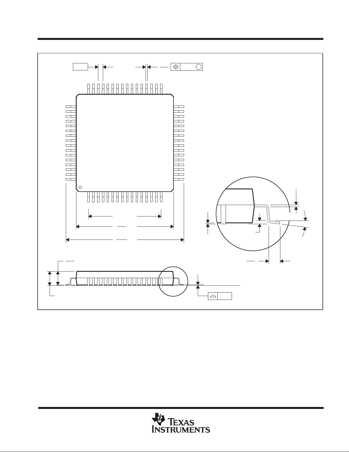
MECHANICAL DATA
MTQF008A – JANUARY 1995 – REVISED DECEMBER 1996
PM (S-PQFP-G64) PLASTIC QUAD FLATPACK
49
64
0,50
48
0,27
0,17
33
1
7,50 TYP
10,20
SQ
9,80
12,20
SQ
11,80
16
0,08
32
17
M
0,05 MIN
0,13 NOM
Gage Plane
0,25
0°–7°
1,45
1,35
1,60 MAX
NOTES: A. All linear dimensions are in millimeters.
B. This drawing is subject to change without notice.
C. Falls within JEDEC MS-026
D. May also be thermally enhanced plastic with leads connected to the die pads.
0,75
0,45
Seating Plane
0,08
4040152/C 11/96
POST OFFICE BOX 655303 • DALLAS, TEXAS 75265
1
Page 42

IMPORTANT NOTICE
Texas Instruments Incorporated and its subsidiaries (TI) reserve the right to make corrections, modifications, enhancements, improvements,
and other changes to its products and services at any time and to discontinue any product or service without notice. Customers should
obtain the latest relevant information before placing orders and should verify that such information is current and complete. All products are
sold subject to TI’s terms and conditions of sale supplied at the time of order acknowledgment.
TI warrants performance of its hardware products to the specifications applicable at the time of sale in accordance with TI’s standard
warranty. Testing and other quality control techniques are used to the extent TI deems necessary to support this warranty. Except where
mandated by government requirements, testing of all parameters of each product is not necessarily performed.
TI assumes no liability for applications assistance or customer product design. Customers are responsible for their products and
applications using TI components. To minimize the risks associated with customer products and applications, customers should provide
adequate design and operating safeguards.
TI does not warrant or represent that any license, either express or implied, is granted under any TI patent right, copyright, mask work right,
or other TI intellectual property right relating to any combination, machine, or process in which TI products or services are used. Information
published by TI regarding third-party products or services does not constitute a license from TI to use such products or services or a
warranty or endorsement thereof. Use of such information may require a license from a third party under the patents or other intellectual
property of the third party, or a license from TI under the patents or other intellectual property of TI.
Reproduction of TI information in TI data books or data sheets is permissible only if reproduction is without alteration and is accompanied
by all associated warranties, conditions, limitations, and notices. Reproduction of this information with alteration is an unfair and deceptive
business practice. TI is not responsible or liable for such altered documentation. Information of third parties may be subject to additional
restrictions.
Resale of TI products or services with statements different from or beyond the parameters stated by TI for that product or service voids all
express and any implied warranties for the associated TI product or service and is an unfair and deceptive business practice. TI is not
responsible or liable for any such statements.
TI products are not authorized for use in safety-critical applications (such as life support) where a failure of the TI product would reasonably
be expected to cause severe personal injury or death, unless officers of the parties have executed an agreement specifically governing
such use. Buyers represent that they have all necessary expertise in the safety and regulatory ramifications of their applications, and
acknowledge and agree that they are solely responsible for all legal, regulatory and safety-related requirements concerning their products
and any use of TI products in such safety-critical applications, notwithstanding any applications-related information or support that may be
provided by TI. Further, Buyers must fully indemnify TI and its representatives against any damages arising out of the use of TI products in
such safety-critical applications.
TI products are neither designed nor intended for use in military/aerospace applications or environments unless the TI products are
specifically designated by TI as military-grade or "enhanced plastic." Only products designated by TI as military-grade meet military
specifications. Buyers acknowledge and agree that any such use of TI products which TI has not designated as military-grade is solely at
the Buyer's risk, and that they are solely responsible for compliance with all legal and regulatory requirements in connection with such use.
TI products are neither designed nor intended for use in automotive applications or environments unless the specific TI products are
designated by TI as compliant with ISO/TS 16949 requirements. Buyers acknowledge and agree that, if they use any non-designated
products in automotive applications, TI will not be responsible for any failure to meet such requirements.
Following are URLs where you can obtain information on other Texas Instruments products and application solutions:
Products Applications
Amplifiers amplifier.ti.com Audio www.ti.com/audio
Data Converters dataconverter.ti.com Automotive www.ti.com/automotive
DSP dsp.ti.com Broadband www.ti.com/broadband
Clocks and Timers www.ti.com/clocks Digital Control www.ti.com/digitalcontrol
Interface interface.ti.com Medical www.ti.com/medical
Logic logic.ti.com Military www.ti.com/military
Power Mgmt power.ti.com Optical Networking www.ti.com/opticalnetwork
Microcontrollers microcontroller.ti.com Security www.ti.com/security
RFID www.ti-rfid.com Telephony www.ti.com/telephony
RF/IF and ZigBee® Solutions www.ti.com/lprf Video & Imaging www.ti.com/video
Mailing Address: Texas Instruments, Post Office Box 655303, Dallas, Texas 75265
Copyright © 2008, Texas Instruments Incorporated
Wireless www.ti.com/wireless
 Loading...