

MSP430F42x0
40 C to 85 C
MIXED SIGNAL MICROCONTROLLER
SLAS455D − MARCH 2005 − REVISED APRIL 2007
D Low Supply-Voltage Range, 1.8 V to 3.6 V
D Ultralow-Power Consumption:
Active Mode: 250 μA at 1 MHz, 2.2 V
Standby Mode: 1.1 μA
Off Mode (RAM Retention): 0.1 μA
D Five Power Saving Modes
D Wake-Up From Standby Mode in Less
Than 6 μs
D 16-Bit RISC Architecture,
125-ns Instruction Cycle Time
D 16-Bit Sigma-Delta A/D Converter With
Internal Reference and Five Differential
Analog Inputs
D 12-Bit D/A Converter
D 16-Bit Timer_A With Three
Capture/Compare Registers
D Brownout Detector
D Bootstrap Loader
D Serial Onboard Programming,
No External Programming Voltage Needed
Programmable Code Protection by Security
Fuse
D Integrated LCD Driver With Contrast
Control for Up to 56 Segments
D MSP430x42x0 Family Members Include:
MSP430F4250: 16KB+256B Flash Memory
256B RAM
MSP430F4260: 24KB+256B Flash Memory
256B RAM
MSP430F4270: 32KB+256B Flash Memory
256B RAM
D For Complete Module Descriptions, See
The MSP430x4xx Family User’s Guide,
Literature Number SLAU056
D For Additional Device Information, See The
MSP430F42x0 Device Erratasheet,
Literature Number SLAZ022
description
The Texas Instruments MSP430 family of ultralow-power microcontrollers consist of several devices featuring
different sets of peripherals targeted for various applications. The architecture, combined with five low power
modes, is optimized to achieve extended battery life in portable measurement applications. The device features
a powerful 16-bit RISC CPU, 16-bit registers, and constant generators that contribute to maximum code
efficiency. The digitally controlled oscillator (DCO) allows wake-up from low-power modes to active mode in less
than 6 μs.
The MSP430F42x0 is a microcontroller configuration with a 16-bit timer, a high performance 16-bit sigma-delta
A/D converter, 12-bit D/A converter, 32 I/O pins, and a liquid crystal display driver.
Typical applications for this device include analog and digital sensor systems, digital motor control, remote
controls, thermostats, digital timers, hand-held meters, etc.
AVAILABLE OPTIONS
PACKAGED DEVICES
T
A
−40°C to 85°C
This integrated circuit can be damaged by ESD. Texas Instruments recommends that all integrated circuits be handled with
appropriate precautions. Failure to observe proper handling and installation procedures can cause damage. ESD damage can range
from subtle performance degradation to complete device failure. Precision integrated circuits may be more susceptible to damage
because very small parametric changes could cause the device not to meet its published specifications. These devices have limited
built-in ESD protection.
Please be aware that an important notice concerning availability, standard warranty, and use in critical applications of
Texas Instruments semiconductor products and disclaimers thereto appears at the end of this data sheet.
PRODUCTION DATA information is current as of publication date.
Products conform to specifications per the terms of Texas Instruments
standard warranty. Production processing does not necessarily include
testing of all parameters.
PLASTIC 48-PIN SSOP
(DL)
MSP430F4250IDL MSP430F4250IRGZ
MSP430F4260IDL MSP430F4260IRGZ
MSP430F4270IDL MSP430F4270IRGZ
PLASTIC 48-PIN QFN
(RGZ)
Copyright © 2007, Texas Instruments Incorporated
POST OFFICE BOX 655303 • DALLAS, TEXAS 75265
1
MSP430F42x0
MIXED SIGNAL MICROCONTROLLER
SLAS455D − MARCH 2005 − REVISED APRIL 2007
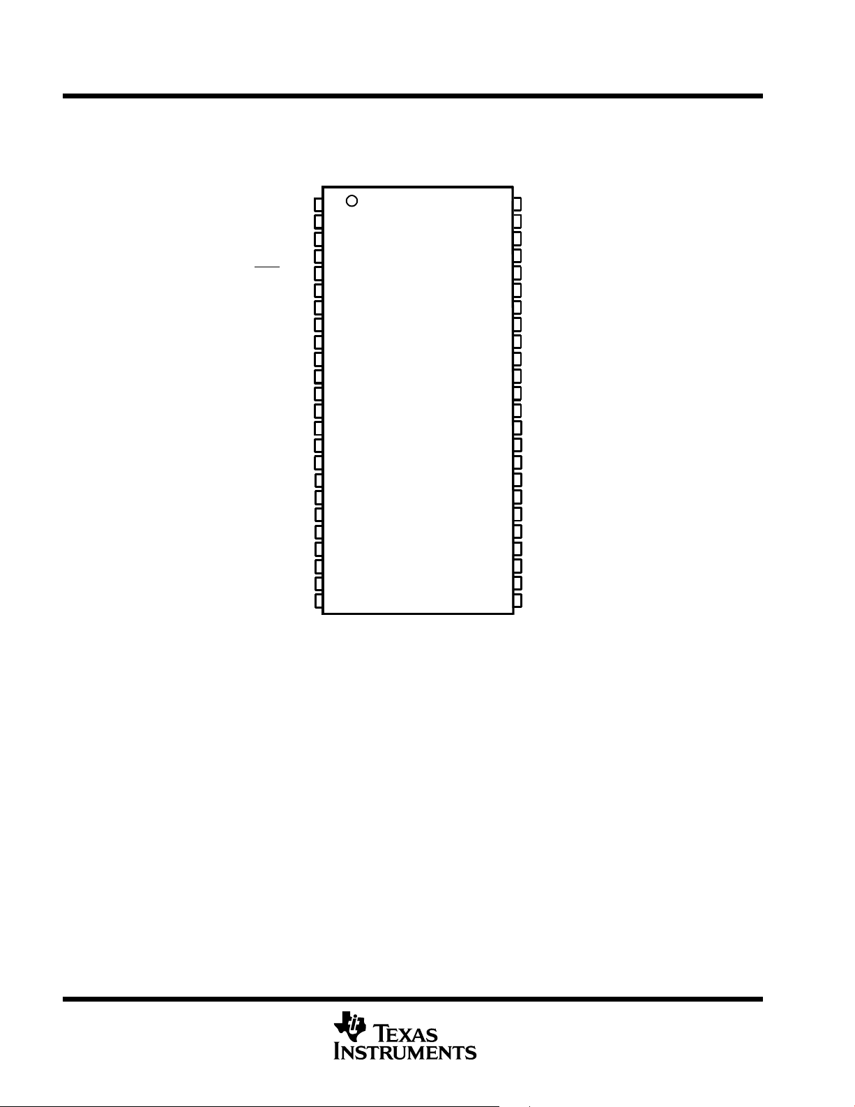
pin designation, MSP430F42x0
DL PACKAGE
(TOP VIEW)
TDO/TDI
TDI/TCLK
TMS
TCK
RST
/NMI
DV
CC
DV
SS
XIN
XOUT
AV
SS
AV
CC
V
REF
P6.0/A0+
P6.1/A0−
P6.2/A1+
P6.3/A1−
P6.4
P6.5
P6.6
P6.7
P1.7/A2+
P1.6/A2−
P1.5/TACLK/ACLK/A3+
P1.4/A3−/DAC0
1
2
3
4
5
6
7
8
MSP430F42x0IDL
9
10
11
12
13
14
15
16
17
18
19
20
21
22
23
24
48
47
46
45
44
43
42
41
40
39
38
37
36
35
34
33
32
31
30
29
28
27
26
25
P5.4/COM3
P5.3/COM2
P5.2/COM1
COM0
P2.0/S13
P2.1/S12
P2.2/S11
P2.3/S10
P2.4/S9
P2.5/S8
P2.6/S7
P2.7/S6
S5
P5.7/S4
P5.6/S3
P5.5/S2
P5.0/S1
P5.1/S0
LCDCAP/R23
LCDREF/R13
P1.0/TA0
P1.1/TA0/MCLK
P1.2/TA1/A4−
P1.3/TA2/A4+
2
POST OFFICE BOX 655303 • DALLAS, TEXAS 75265
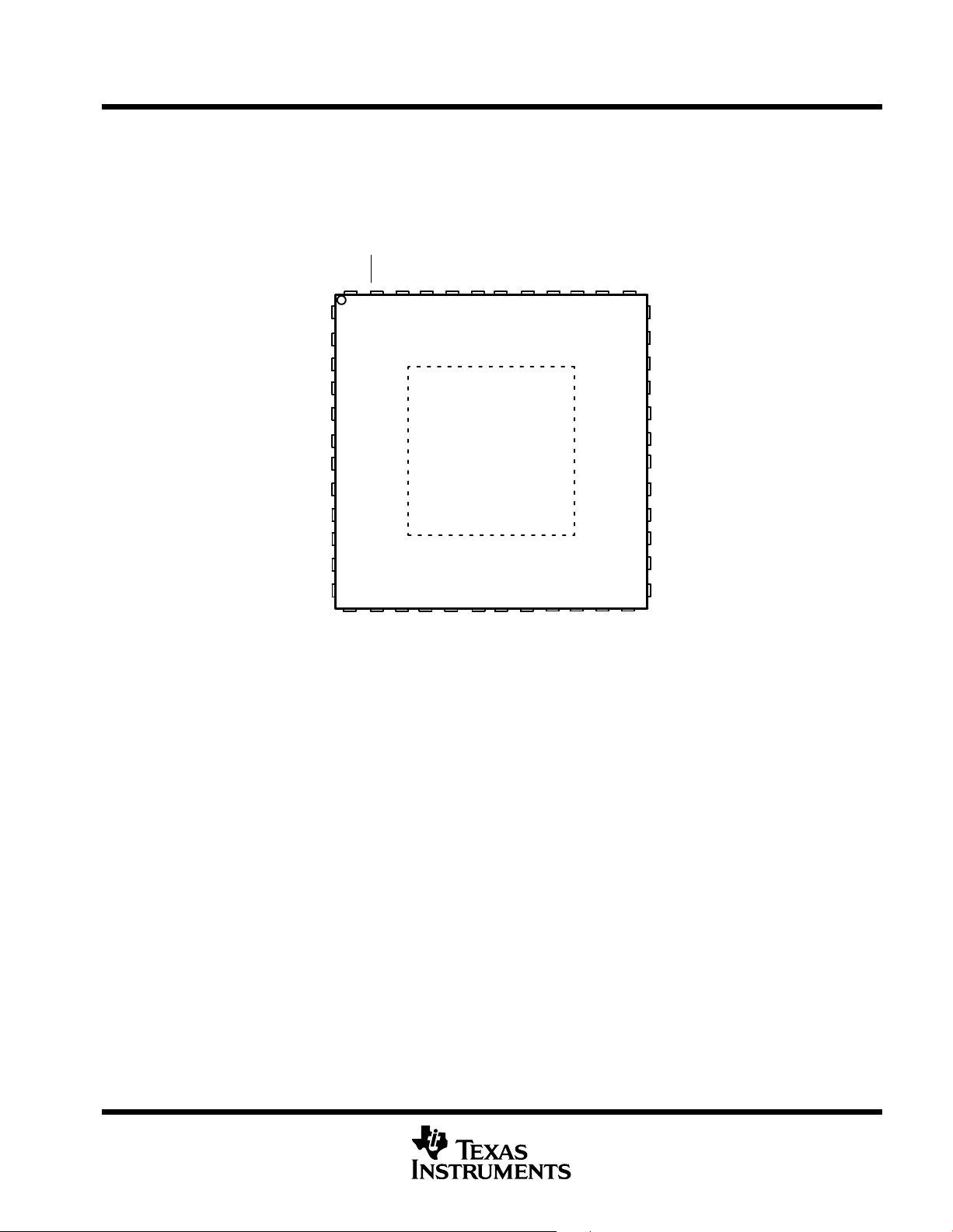
pin designation, MSP430F42x0 (continued)
CC
RST/NMI
DV
SS
XIN
XOUT
AV
SS
AV
CC
V
REF
P6.0/A0+
P6.1/A0−
P6.2/A1+
P6.3/A1−
P6.4
P6.5
DV
1
2
3
4
5
6
7
8
9
10
11
12
TCK
TMS
46 45 44 43 42 41 40 39 38
47
MSP430F42x0IRGZ
14
15 16 17 18 19 20 21 22 23
RGZ PACKAGE
(TOP VIEW)
TDI/TCLK
TDO/TDI
P5.4/COM3
MSP430F42x0
MIXED SIGNAL MICROCONTROLLER
SLAS455D − MARCH 2005 − REVISED APRIL 2007
P5.3/COM2
P5.2/COM1
COM0
P2.0/S13
P2.1/S12
P2.2/S11
36
P2.3/S10
35
P2.4/S9
34
P2.5/S8
33
P2.6/S7
32
P2.7/S6
31
S5
30
P5.7/S4
29
P5.6/S3
28
P5.5/S2
27
P5.0/S1
26
P5.1/S0
25
P6.6
P6.7
P1.6/A2−
P1.7/A2+
P1.2/TA1/A4−
P1.3/TA2/A4+
P1.4/A3−/DAC0
P1.5/TACLK/ACLK/A3+
P1.0/TA0
P1.1/TA0/MCLK
LCDREF/R13
LCDCAP/R23
POST OFFICE BOX 655303 • DALLAS, TEXAS 75265
3
MSP430F42x0
MIXED SIGNAL MICROCONTROLLER
SLAS455D − MARCH 2005 − REVISED APRIL 2007
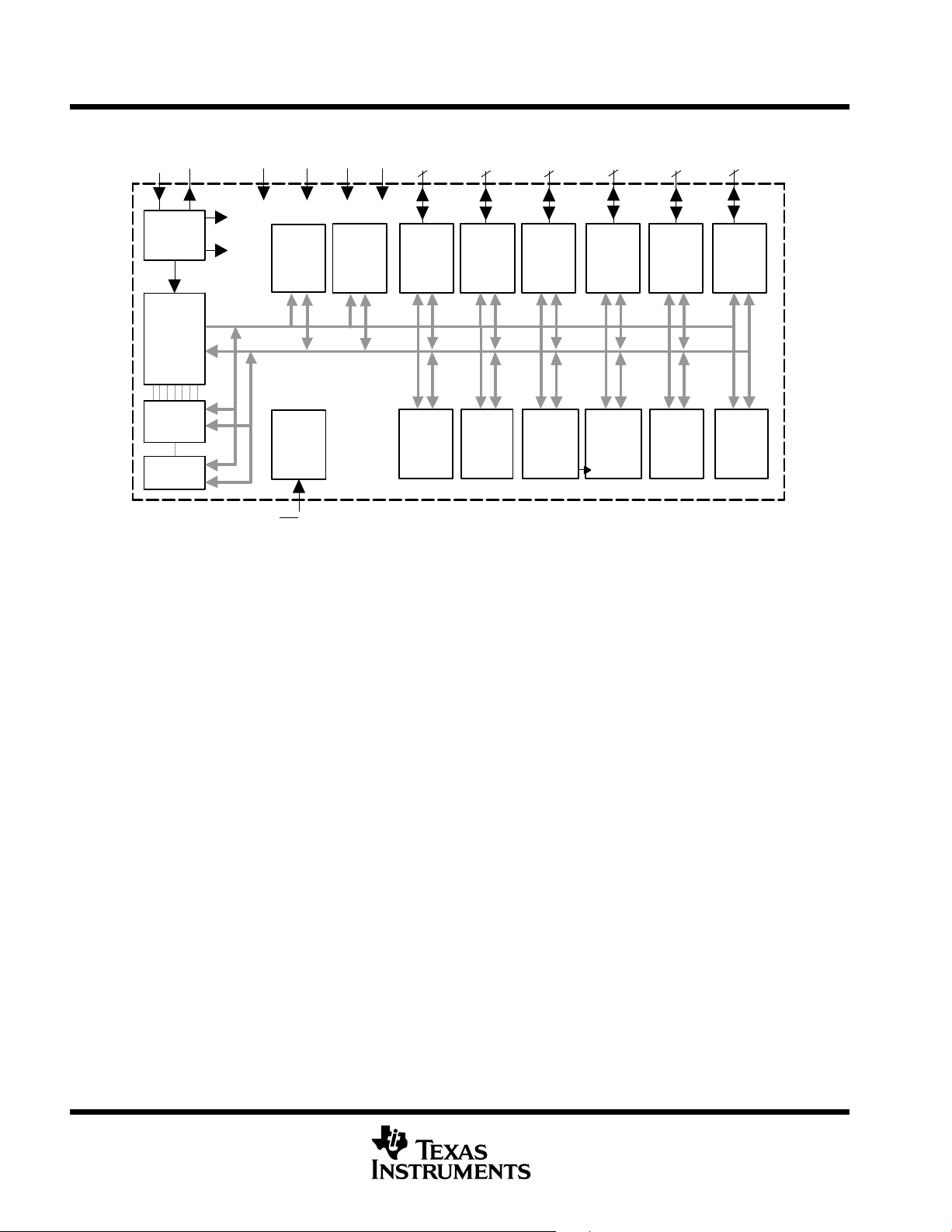
MSP430F42x0 functional block diagram
XIN
Oscillator
FLL+
8 MHz
CPU
incl. 16
Registers
Emulation
Module
JTAG
Interface
XOUT
MCLK
DVCCDVSSAVCCAV
ACLK
MAB
MDB
Flash
32KB
24KB
16KB
POR/
Brownout
RST/NMI
SMCLK
RAM
256B
SS
P1
8
Port 1
8 I/O
Interrupt
Capability
Watchdog
Timer+
WDT+
15/16-Bit
P2
8
Port 2
8 I/O
Interrupt
Capability
Timer_A3
3 CC Reg
P3
8
Port 3
8 I/O
Basic
Timer 1
1 Interrupt
Vector
Segments
1,2,3,4 MUX
f
LCD
P4
Port 4
8 I/O
LCD_A
56
8
P6
8
Port 6
8 I/O
DAC12
12 Bit
1 Channel
Voltage Out
8
P5
Port 5
8 I/O
SD16_A
16 Bit
4
POST OFFICE BOX 655303 • DALLAS, TEXAS 75265
MSP430F42x0
MIXED SIGNAL MICROCONTROLLER
SLAS455D − MARCH 2005 − REVISED APRIL 2007
MSP430F42x0 Terminal Functions
TERMINAL
NAME DL
TDO/TDI 1 43 I/O Test data output port. TDO/TDI data output or programming data input terminal
TDI/TCLK 2 44 I Test data input or test clock input. The device protection fuse is connected to TDI/TCLK.
TMS 3 45 I Test mode select. TMS is used as an input port for device programming and test.
TCK 4 46 I Test clock. TCK is the clock input port for device programming and test.
RST/NMI 5 47 I General-purpose digital I/O / reset input or nonmaskable interrupt input port
DV
CC
DV
SS
XIN 8 2 I Input terminal of crystal oscillator XT1
XOUT 9 3 O Output terminal of crystal oscillator XT1
AV
SS
AV
CC
V
REF
P6.0/A0+ 13 7 I/O General-purpose digital I/O / analog input A0+
P6.1/A0− 14 8 I/O General-purpose digital I/O / analog input A0−
P6.2/A1+ 15 9 I/O General-purpose digital I/O / analog input A1+
P6.3/A1− 16 10 I/O General-purpose digital I/O / analog input A1−
P6.4 17 11 I/O General-purpose digital I/O
P6.5 18 12 I/O General-purpose digital I/O
P6.6 19 13 I/O General-purpose digital I/O
P6.7 20 14 I/O General-purpose digital I/O
P1.7/A2+ 21 15 I/O General-purpose digital I/O / analog input A2+
P1.6/A2− 22 16 I/O General-purpose digital I/O / analog input A2−
P1.5/TACLK/ACLK/A3+ 23 17 I/O
P1.4/A3−/DAC0 24 18 I/O General-purpose digital I/O / analog input A3− / DAC12 output
P1.3/TA2/A4+ 25 19 I/O
P1.2/TA1/A4− 26 20 I/O
P1.1/TA0/MCLK 27 21 I/O
P1.0/TA0 28 22 I/O
LCDREF/R13 29 23 External LCD reference voltage input / input port of third most positive analog LCD level (V4
LCDCAP/R23 30 24 Capacitor connection for LCD charge pump /
P5.1/S0 31 25 I/O General-purpose digital I/O / LCD segment output 0
P5.0/S1 32 26 I/O General-purpose digital I/O / LCD segment output 1
P5.5/S2 33 27 I/O General-purpose digital I/O / LCD segment output 2
P5.6/S3 34 28 I/O General-purpose digital I/O / LCD segment output 3
P5.7/S4 35 29 I/O General-purpose digital I/O / LCD segment output 4
S5 36 30 O LCD segment output 5
P2.7/S6 37 31 I/O General-purpose digital I/O / LCD segment output 6
P2.6/S7 38 32 I/O General-purpose digital I/O / LCD segment output 7
RGZ
NO.
I/O
General-purpose digital I/O / Timer_A, clock signal TACLK input /
ACLK output (divided by 1, 2, 4, or 8) / analog input A3+
General-purpose digital I/O / Timer_A, Capture: CCI2A, compare: Out2 output /
analog input A4+
General-purpose digital I/O / Timer_A, Capture: CCI1A, compare: Out1 output /
analog input A4−
General-purpose digital I/O / Timer_A. Capture: CCI0B / MCLK output. Note: TA0 is only an
input on this pin / BSL Receive
General-purpose digital I/O / Timer_A. Capture: CCI0A input, compare: Out0 output / BSL
Transmit
or V3)
input port of second most positive analog LCD level (V2)
NO.
6 48 Digital supply voltage, positive terminal
7 1 Digital supply voltage, negative terminal
10 4 Analog supply voltage, negative terminal
11 5 Analog supply voltage, positive terminal
12 6 I/O Analog reference voltage
DESCRIPTION
POST OFFICE BOX 655303 • DALLAS, TEXAS 75265
5
MSP430F42x0
MIXED SIGNAL MICROCONTROLLER
SLAS455D − MARCH 2005 − REVISED APRIL 2007
MSP430F42x0 Terminal Functions (Continued)
TERMINAL
NAME DL
P2.5/S8 39 33 I/O General-purpose digital I/O / LCD segment output 8
P2.4/S9 40 34 I/O General-purpose digital I/O / LCD segment output 9
P2.3/S10 41 35 I/O General-purpose digital I/O / LCD segment output 10
P2.2/S11 42 36 I/O General-purpose digital I/O / LCD segment output 11
P2.1/S12 43 37 I/O General-purpose digital I/O / LCD segment output 12
P2.0/S13 44 38 I/O General-purpose digital I/O / LCD segment output 13
COM0 45 39 O Common output, COM0−3 are used for LCD backplanes.
P5.2/COM1 46 40 I/O General-purpose digital I/O / common output, COM0−3 are used for LCD backplanes.
P5.3/COM2 47 41 I/O General-purpose digital I/O / common output, COM0−3 are used for LCD backplanes.
P5.4/COM3 48 42 I/O General-purpose digital I/O / common output, COM0−3 are used for LCD backplanes.
QFN Pad NA None NA QFN package pad connection to DVSS recommended.
NO.
RGZ
NO.
I/O
DESCRIPTION
6
POST OFFICE BOX 655303 • DALLAS, TEXAS 75265
short-form description
CPU
MSP430F42x0
MIXED SIGNAL MICROCONTROLLER
SLAS455D − MARCH 2005 − REVISED APRIL 2007
The MSP430 CPU has a 16-bit RISC architecture
that is highly transparent to the application. All
operations, other than program-flow instructions,
are performed as register operations in
conjunction with seven addressing modes for
source operand and four addressing modes for
destination operand.
The CPU is integrated with 16 registers that
provide reduced instruction execution time. The
register-to-register operation execution time is
one cycle of the CPU clock.
Four of the registers, R0 to R3, are dedicated as
program counter, stack pointer, status register,
and constant generator respectively. The
remaining registers are general-purpose
registers.
Peripherals are connected to the CPU using data,
address, and control buses, and can be handled
with all instructions.
instruction set
The instruction set consists of 51 instructions with
three formats and seven address modes. Each
instruction can operate on word and byte data.
Table 1 shows examples of the three types of
instruction formats; the address modes are listed
in Table 2.
Program Counter
Stack Pointer
Status Register
Constant Generator
General-Purpose Register
General-Purpose Register
General-Purpose Register
General-Purpose Register
General-Purpose Register
General-Purpose Register
General-Purpose Register
General-Purpose Register
General-Purpose Register
General-Purpose Register
General-Purpose Register
General-Purpose Register
PC/R0
SP/R1
SR/CG1/R2
CG2/R3
R4
R5
R6
R7
R8
R9
R10
R11
R12
R13
R14
R15
Table 1. Instruction Word Formats
Dual operands, source-destination e.g. ADD R4,R5 R4 + R5 −−−> R5
Single operands, destination only e.g. CALL R8 PC −−>(TOS), R8−−> PC
Relative jump, un/conditional e.g. JNE Jump-on-equal bit = 0
Table 2. Address Mode Descriptions
ADDRESS MODE S D SYNTAX EXAMPLE OPERATION
Register F
Indexed F F MOV X(Rn),Y(Rm) MOV 2(R5),6(R6) M(2+R5)—> M(6+R6)
Symbolic (PC relative) F F MOV EDE,TONI M(EDE) —> M(TONI)
Absolute F F MOV & MEM, & TCDAT M(MEM) —> M(TCDAT)
Indirect F MOV @Rn,Y(Rm) MOV @R10,Tab(R6) M(R10) —> M(Tab+R6)
Indirect
autoincrement
Immediate F MOV #X,TONI MOV #45,TONI #45 —> M(TONI)
NOTE: S = source D = destination
F
F MOV @Rn+,Rm MOV @R10+,R11
MOV Rs,Rd MOV R10,R11 R10 —> R11
M(R10) —> R11
R10 + 2—> R10
POST OFFICE BOX 655303 • DALLAS, TEXAS 75265
7

MSP430F42x0
MIXED SIGNAL MICROCONTROLLER
SLAS455D − MARCH 2005 − REVISED APRIL 2007
operating modes
The MSP430 has one active mode and five software selectable low-power modes of operation. An interrupt
event can wake up the device from any of the five low-power modes, service the request and restore back to
the low-power mode on return from the interrupt program.
The following six operating modes can be configured by software:
D Active mode (AM)
− All clocks are active
D Low-power mode 0 (LPM0)
− CPU is disabled
ACLK and SMCLK remain active, MCLK is available to modules
FLL+ loop control remains active
D Low-power mode 1 (LPM1)
− CPU is disabled
ACLK and SMCLK remain active, MCLK is available to modules
FLL+ loop control is disabled
D Low-power mode 2 (LPM2)
− CPU is disabled
MCLK, FLL+ loop control, and DCOCLK are disabled
DCO’s dc-generator remains enabled
ACLK remains active
D Low-power mode 3 (LPM3)
− CPU is disabled
MCLK, FLL+ loop control, and DCOCLK are disabled
DCO’s dc-generator is disabled
ACLK remains active
D Low-power mode 4 (LPM4);
− CPU is disabled
ACLK is disabled
MCLK, FLL+ loop control, and DCOCLK are disabled
DCO’s dc-generator is disabled
Crystal oscillator is stopped
8
POST OFFICE BOX 655303 • DALLAS, TEXAS 75265
MSP430F42x0
MIXED SIGNAL MICROCONTROLLER
SLAS455D − MARCH 2005 − REVISED APRIL 2007
interrupt vector addresses
The interrupt vectors and the power-up starting address are located in the address range 0FFFFh−0FFE0h. The
vector contains the 16-bit address of the appropriate interrupt-handler instruction sequence.
Table 3. Interrupt Sources, Flags, and Vectors of MSP430F42x0 Configuration
INTERRUPT SOURCE INTERRUPT FLAG SYSTEM INTERRUPT
Power-Up
External Reset
Watchdog
Flash Memory
PC Out-of-Range (see Note 4)
NMI
Oscillator Fault
Flash Memory Access Violation
SD16_A
Watchdog Timer WDTIFG Maskable 0FFF4h 10
Timer_A3 TACCR0 CCIFG0 (see Note 2) Maskable 0FFECh 6
Timer_A3
I/O Port P1 (Eight Flags) P1IFG.0 to P1IFG.7 (see Notes 1 and 2) Maskable 0FFE8h 4
DAC12 DAC12_0IFG
I/O Port P2 (Eight Flags) P2IFG.0 to P2IFG.7 (see Notes 1 and 2) Maskable 0FFE2h 1
Basic Timer1 BTIFG Maskable 0FFE0h 0, lowest
NOTES: 1. Multiple source flags
2. Interrupt flags are located in the module.
3. (Non)maskable: the individual interrupt-enable bit can disable an interrupt event, but the general-interrupt enable cannot
disable it.
4. A reset is generated if the CPU tries to fetch instructions from within the module register memory address range (0h−01FFh) or from
within unused address ranges (MSP430F4270, MSP430F4260: from 0300h to 0BFFh and from 01100h to 07FFFh,
MSP430F4250: from 0300h to 0BFFh and from 01100h to 0BFFFh).
NMIIFG (see Notes 1 and 3)
OFIFG (see Notes 1 and 3)
ACCVIFG (see Notes 1 and 3)
SD16CCTLx SD16OVIFG,
TACCR1 CCIFG1 and TACCR2 CCIFG2,
TAIFG (see Notes 1 and 2)
WDTIFG
KEYV
(see Note 1)
SD16CCTLx SD16IFG
(see Notes 1 and 2)
(see Note 2)
Reset 0FFFEh 15, highest
(Non)maskable
(Non)maskable
(Non)maskable
Maskable 0FFF8h 12
Maskable 0FFEAh 5
Maskable 0FFE6h 3
WORD
ADDRESS
0FFFCh 14
0FFFAh 13
0FFF6h 11
0FFF2h 9
0FFF0h 8
0FFEEh 7
0FFE4h 2
PRIORITY
POST OFFICE BOX 655303 • DALLAS, TEXAS 75265
9
MSP430F42x0
MIXED SIGNAL MICROCONTROLLER
SLAS455D − MARCH 2005 − REVISED APRIL 2007
special function registers
The MSP430 special function registers(SFR) are located in the lowest address space, and are organized as
byte mode registers. SFRs should be accessed with byte instructions.
interrupt enable registers 1 and 2
Address
0h ACCVIE NMIIE
7654 0
rw–0
rw–0 rw–0 rw–0
321
WDTIE: Watchdog-timer interrupt enable. Inactive if watchdog mode is selected.
Active if watchdog timer is configured as a general-purpose timer.
OFIE: Oscillator-fault-interrupt enable
NMIIE: Nonmaskable-interrupt enable
ACCVIE: Flash access violation interrupt enable
Address
01h
7654 0321
BTIE
rw–0
BTIE: Basic timer interrupt enable
interrupt flag registers 1 and 2
Address
02h NMIIFG
7654 0
rw–0 rw–1 rw–(0)
WDTIFG: Set on watchdog timer overflow (in watchdog mode) or security key violation
Reset on V
power-on or a reset condition at the RST/NMI pin in reset mode
CC
OFIFG: Flag set on oscillator fault
NMIIFG: Set via RST
/NMI pin
321
OFIE WDTIE
OFIFG WDTIFG
Address
03h
7654 0321
BTIFG
rw–0
BTIFG: Basic timer flag
10
POST OFFICE BOX 655303 • DALLAS, TEXAS 75265
module enable registers 1 and 2
MSP430F42x0
MIXED SIGNAL MICROCONTROLLER
SLAS455D − MARCH 2005 − REVISED APRIL 2007
Address
04h
Address
05h
Legend: rw:
rw–0,1:
rw–(0,1):
7654 0321
7654 0321
Bit Can Be Read and Written
Bit Can Be Read and Written. It Is Reset or Set by PUC.
Bit Can Be Read and Written. It Is Reset or Set by POR.
SFR Bit Not Present in Device
memory organization
MSP430F4250 MSP430F4260 MSP430F4270
Memory
Main: interrupt vector
Main: code memory
Information memory Size
Boot memory Size
RAM Size 256 Byte
Peripherals 16-bit
Size
Flash
Flash
Flash
ROM
8-bit
8-bit SFR
16KB
0FFFFh − 0FFE0h
0FFFFh − 0C000h
256 Byte
010FFh − 01000h
1KB
0FFFh − 0C00h
02FFh − 0200h
01FFh − 0100h
0FFh − 010h
0Fh − 00h
24KB
0FFFFh − 0FFE0h
0FFFFh − 0A000h
256 Byte
010FFh − 01000h
1KB
0FFFh − 0C00h
256 Byte
02FFh − 0200h
01FFh − 0100h
0FFh − 010h
0Fh − 00h
32KB
0FFFFh − 0FFE0h
0FFFFh − 08000h
256 Byte
010FFh − 01000h
1KB
0FFFh − 0C00h
256 Byte
02FFh − 0200h
01FFh − 0100h
0FFh − 010h
0Fh − 00h
bootstrap loader (BSL)
The MSP430 bootstrap loader (BSL) enables users to program the flash memory or RAM using a UART serial
interface. Access to the MSP430 memory via the BSL is protected by user-defined password. For complete
description of the features of the BSL and its implementation, see the Application report Features of the MSP430
Bootstrap Loader, Literature Number SLAA089.
BSL Function DL Package Pins RGZ Package Pins
Data Transmit 28 − P1.0 22 − P1.0
Data Receive 27 − P1.1 21 − P1.1
POST OFFICE BOX 655303 • DALLAS, TEXAS 75265
11
MSP430F42x0
MIXED SIGNAL MICROCONTROLLER
SLAS455D − MARCH 2005 − REVISED APRIL 2007
flash memory
The flash memory can be programmed via the JTAG port, the bootstrap loader, or in-system by the CPU. The
CPU can perform single-byte and single-word writes to the flash memory. Features of the flash memory include:
D Flash memory has n segments of main memory and two segments of information memory (A and B) of 128
bytes each. Each segment in main memory is 512 bytes in size.
D Segments 0 to n may be erased in one step, or each segment may be individually erased.
D Segments A and B can be erased individually, or as a group with segments 0−n.
Segments A and B are also called information memory.
D New devices may have some bytes programmed in the information memory (needed for test during
manufacturing). The user should perform an erase of the information memory prior to the first use.
16KB
24KB
32KB
0FFFFh
0FE00h
0FDFFh
0FC00h
0FBFFh
0FA00h
0F9FFh
0C400h
0C3FFh
0C200h
0C1FFh
0C000h
010FFh
01080h
0107Fh
01000h
0FFFFh
0FE00h
0FDFFh
0FC00h
0FBFFh
0FA00h
0F9FFh
0A400h
0A3FFh
0A200h
0A1FFh
0A000h
010FFh
01080h
0107Fh
01000h
0FFFFh
0FE00h
0FDFFh
0FC00h
0FBFFh
0FA00h
0F9FFh
08400h
083FFh
08200h
081FFh
08000h
010FFh
01080h
0107Fh
01000h
Segment 0
w/ Interrupt Vectors
Segment 1
Segment 2
Main
Memory
Segment n-1
Segment n†
Segment A
Information
Memory
Segment B
12
POST OFFICE BOX 655303 • DALLAS, TEXAS 75265

MSP430F42x0
MIXED SIGNAL MICROCONTROLLER
SLAS455D − MARCH 2005 − REVISED APRIL 2007
peripherals
Peripherals are connected to the CPU through data, address, and control busses and can be handled using
all instructions. For complete module descriptions, refer to the MSP430x4xx Family User’s Guide, Literature
Number SLAU056.
oscillator and system clock
The clock system in the MSP430F42x0 family of devices is supported by the FLL+ module that includes support
for a 32768 Hz watch crystal oscillator, an internal digitally-controlled oscillator (DCO) and a high frequency
crystal oscillator. The FLL+ clock module is designed to meet the requirements of both low system cost and
low-power consumption. The FLL+ features digital frequency locked loop (FLL) hardware which in conjunction
with a digital modulator stabilizes the DCO frequency to a programmable multiple of the watch crystal frequency.
The internal DCO provides a fast turn-on clock source and stabilizes in less than 6 μs. The FLL+ module
provides the following clock signals:
D Auxiliary clock (ACLK), sourced from a 32768 Hz watch crystal or a high frequency crystal.
D Main clock (MCLK), the system clock used by the CPU.
D Sub-Main clock (SMCLK), the sub-system clock used by the peripheral modules.
D ACLK/n, the buffered output of ACLK, ACLK/2, ACLK/4, or ACLK/8.
brownout
The brownout circuit is implemented to provide the proper internal reset signal to the device during power-on
and power-off. The CPU begins code execution after the brownout circuit releases the device reset. However,
V
may not have ramped to V
CC
changed until V
reaches V
CC
CC(min)
CC(min)
at that time. The user must insure the default FLL+ settings are not
.
digital I/O
There are four 8-bit I/O ports implemented—ports P1, P2, P5 and P6:
D All individual I/O bits are independently programmable.
D Any combination of input, output, and interrupt conditions is possible.
D Edge-selectable interrupt input capability for all the eight bits of ports P1 and P2.
D Read/write access to port-control registers is supported by all instructions.
Basic Timer1
The Basic Timer1 has two independent 8-bit timers which can be cascaded to form a 16-bit timer/counter. Both
timers can be read and written by software. The Basic Timer1 can be used to generate periodic interrupts.
LCD driver with regulated charge pump
The LCD_A driver generates the segment and common signals required to drive an LCD display. The LCD_A
controller has dedicated data memory to hold segment drive information. Common and segment signals are
generated as defined by the mode. Static, 2−MUX, 3−MUX, and 4−MUX LCDs are supported by this peripheral.
The module can provide a LCD voltage independent of the supply voltage via an integrated charge pump.
Furthermore it is possible to control the level of the LCD voltage and thus contrast in software.
watchdog timer
The primary function of the watchdog timer (WDT+) module is to perform a controlled system restart after a
software problem occurs. If the selected time interval expires, a system reset is generated. If the watchdog
function is not needed in an application, the module can be configured as an interval timer and can generate
interrupts at selected time intervals.
POST OFFICE BOX 655303 • DALLAS, TEXAS 75265
13
MSP430F42x0
Device Input
Module
Module
Module Output
Si
l
I
Block
Si
l
MIXED SIGNAL MICROCONTROLLER
SLAS455D − MARCH 2005 − REVISED APRIL 2007
timer_A3
Timer_A3 is a 16-bit timer/counter with three capture/compare registers. Timer_A3 can support multiple
capture/compares, PWM outputs, and interval timing. Timer_A3 also has extensive interrupt capabilities.
Interrupts may be generated from the counter on overflow conditions and from each of the capture/compare
registers.
Timer_A3 Signal Connections
Input Pin Number
DL RGZ
23 - P1.5 17 - P1.5 TACLK TACLK
23 - P1.5 17 - P1.5 TACLK INCLK
28 - P1.0 22 - P1.0 TA0 CCI0A
27 - P1.1 21 - P1.1 TA0 CCI0B
26 - P1.2 20 - P1.2 TA1 CCI1A
26 - P1.2 20 - P1.2 TA1 CCI1B
25 - P1.3 19 - P1.3 TA2 CCI2A
Device Input Module Module Module Output
gna
ACLK ACLK
SMCLK SMCLK
DV
SS
DV
CC
DV
SS
DV
CC
ACLK (internal) CCI2B
DV
SS
DV
CC
nput Name
GND
V
CC
GND
V
CC
GND
V
CC
gna
Timer NA
CCR0 TA0
CCR1 TA1
CCR2 TA2
Output Pin Number
DL RGZ
28 - P1.0 22 - P1.0
26 - P1.2 20 - P1.2
25 - P1.3 19 - P1.3
SD16_A
The SD16_A module supports 16-bit analog-to-digital conversions. The module implements a 16-bit
sigma-delta core and reference generator. In addition to external analog inputs, an internal V
CC
temperature sensor are also available.
DAC12
The DAC12 module is a 12-bit, R-ladder, voltage output DAC. The DAC12 may be used in 8- or 12-bit mode.
sense and
14
POST OFFICE BOX 655303 • DALLAS, TEXAS 75265
peripheral file map
y
)
Byte Access)
(see also:
Watchdog Watchdog timer control WDTCTL 0120h
Timer_A3
Flash
DAC12
SD16_A
(see also:
Peripherals with
B
te Access
SD16_A
(see also:
Peripherals with
Word Access)
LCD_A LCD Voltage Control 1
FLL+ Clock
Basic Timer1 BT counter 2
MSP430F42x0
MIXED SIGNAL MICROCONTROLLER
SLAS455D − MARCH 2005 − REVISED APRIL 2007
PERIPHERALS WITH WORD ACCESS
_
_
Capture/compare register 2 TACCR2 0176h
Capture/compare register 1 TACCR1 0174h
Capture/compare register 0 TACCR0 0172h
Timer_A register TAR 0170h
Capture/compare control 2 TACCTL2 0166h
Capture/compare control 1 TACCTL1 0164h
Capture/compare control 0 TACCTL0 0162h
Timer_A control TACTL 0160h
Timer_A interrupt vector TAIV 012Eh
Flash control 3 FCTL3 012Ch
Flash control 2 FCTL2 012Ah
Flash control 1 FCTL1 0128h
DAC12_0 data DAC12_0DAT 01C8h
DAC12_0 control DAC12_0CTL 01C0h
General Control SD16CTL 0100h
Channel 0 Control SD16CCTL0 0102h
Interrupt vector word register SD16IV 0110h
Channel 0 conversion memory SD16MEM0 0112h
PERIPHERALS WITH BYTE ACCESS
Channel 0 Input Control SD16INCTL0 0B0h
Analog Enable SD16AE 0B7h
LCDAVCTL1
LCD Voltage Control 0
LCD Voltage Port Control 1
LCD Voltage Port Control 0
LCD memory 20
:
LCD memory 16
LCD memory 15
:
LCD memory 1
LCD control and mode
FLL+ Control 1 FLL_CTL1 054h
FLL+ Control 0 FLL_CTL0 053h
System clock frequency control SCFQCTL 052h
System clock frequency integrator SCFI1 051h
System clock frequency integrator SCFI0 050h
BT counter 1
BT control
LCDAVCTL0
LCDAPCTL1
LCDAPCTL0
LCDM20
:
LCDM16
LCDM15
:
LCDM1
LCDACTL
BTCNT2
BTCNT1
BTCTL
0AFh
0AEh
0ADh
0ACh
0A4h
:
0A0h
09Fh
:
091h
090h
047h
046h
040h
POST OFFICE BOX 655303 • DALLAS, TEXAS 75265
15

MSP430F42x0
p
MIXED SIGNAL MICROCONTROLLER
SLAS455D − MARCH 2005 − REVISED APRIL 2007
peripheral file map (continued)
PERIPHERALS WITH BYTE ACCESS (CONTINUED)
Port P6
Port P5
Port P2
Port P1
Special functions
Port P6 selection P6SEL 037h
Port P6 direction P6DIR 036h
Port P6 output P6OUT 035h
Port P6 input P6IN 034h
Port P5 selection P5SEL 033h
Port P5 direction P5DIR 032h
Port P5 output P5OUT 031h
Port P5 input P5IN 030h
Port P2 selection P2SEL 02Eh
Port P2 interrupt enable P2IE 02Dh
Port P2 interrupt-edge select P2IES 02Ch
Port P2 interrupt flag P2IFG 02Bh
Port P2 direction P2DIR 02Ah
Port P2 output P2OUT 029h
Port P2 input P2IN 028h
Port P1 selection P1SEL 026h
Port P1 interrupt enable P1IE 025h
Port P1 interrupt-edge select P1IES 024h
Port P1 interrupt flag P1IFG 023h
Port P1 direction P1DIR 022h
Port P1 output P1OUT 021h
Port P1 input P1IN 020h
SFR module enable 2 ME2 005h
SFR module enable 1 ME1 004h
SFR interrupt flag 2 IFG2 003h
SFR interrupt flag 1 IFG1 002h
SFR interrupt enable 2 IE2 001h
SFR interrupt enable 1 IE1 000h
16
POST OFFICE BOX 655303 • DALLAS, TEXAS 75265
MSP430F42x0
(see Note 2)
MIXED SIGNAL MICROCONTROLLER
SLAS455D − MARCH 2005 − REVISED APRIL 2007
absolute maximum ratings over operating free-air temperature (unless otherwise noted)
†
Voltage applied at VCC to VSS −0.3 V to 4.1 V. . . . . . . . . . . . . . . . . . . . . . . . . . . . . . . . . . . . . . . . . . . . . . . . . . . . . .
Voltage applied to any pin (see Note) −0.3 V to V
CC
+ 0.3 V. . . . . . . . . . . . . . . . . . . . . . . . . . . . . . . . . . . . . . . . . .
Diode current at any device terminal . ±2 mA. . . . . . . . . . . . . . . . . . . . . . . . . . . . . . . . . . . . . . . . . . . . . . . . . . . . . .
Storage temperature, T
: (unprogrammed device) −55°C to 150°C. . . . . . . . . . . . . . . . . . . . . . . . . . . . . . . . . .
stg
(programmed device) −40°C to 85°C. . . . . . . . . . . . . . . . . . . . . . . . . . . . . . . . . . . . .
†
Stresses beyond those listed under “absolute maximum ratings” may cause permanent damage to the device. These are stress ratings only, and
functional operation of the device at these or any other conditions beyond those indicated under “recommended operating conditions” is not
implied. Exposure to absolute-maximum-rated conditions for extended periods may affect device reliability.
NOTE: All voltages referenced to V
to the TDI/TCLK pin when blowing the JTAG fuse.
The JTAG fuse-blow voltage, VFB, is allowed to exceed the absolute maximum rating. The voltage is applied
SS.
recommended operating conditions
MIN NOM MAX UNITS
Supply voltage during program execution (see Note 1),
V
(AVCC = DVCC = VCC)
CC
Supply voltage during flash memory programming (see Note 1),
V
(AVCC = DVCC = VCC)
CC
Supply voltage, V
Operating free-air temperature range, T
LFXT1 crystal frequency, f
(see Note 2)
Processor frequency (signal MCLK), f
NOTES: 1. It is recommended to power AVCC and DVCC from the same source. A maximum difference of 0.3 V betweeen AVCC and DVCC can
2. In LF mode, the LFXT1 oscillator requires a watch crystal. In XT1 mode, LFXT1 accepts a ceramic resonator or a crystal.
(AVSS = DVSS = VSS) 0 0 V
SS
A
LF selected,
XTS_FLL=0
(LFXT1)
(System)
be tolerated during power up and operation.
XT1 selected,
XTS_FLL=1
XT1 selected,
XTS_FLL=1
Watch crystal 32.768 kHz
Ceramic resonator 450 8000 kHz
Crystal 1000 8000 kHz
VCC = 1.8 V DC 4.15
VCC = 3.6 V DC 8
1.8 3.6 V
2.5 3.6 V
−40 85 °C
MHz
f
(MHz)
System
8 MHz
4.15 MHz
Supply voltage range,
MSP430F42x0, during
program execution
1.8 3.63
2.5
Supply Voltage − V
Supply voltage range, MSP430F42x0,
during flash memory programming
Figure 1. Frequency vs Supply Voltage, typical characteristic
POST OFFICE BOX 655303 • DALLAS, TEXAS 75265
17
MSP430F42x0
f
(MCLK)
f
(SMCLK)
MHz
Low power mode, (LPM0)
(
f(MCLK) = f (SMCLK) = 0 MHz
Low-power mode, (LPM3)
f
(MCLK)
f
(SMCLK)
MHz,
,
LCD_A enabled, LCDCPEN = 0:
(;
LCD (ACLK)
)
Low-power mode, (LPM3)
f
(MCLK)
f
(SMCLK)
MHz,
V
CC
2.2 V
,
LCD_A enabled, LCDCPEN = 0:
(;
LCD (ACLK)
)
V
CC
V
SCG0
(see Note
)
f
SCG0
(see Note 2 and Note 4)
MIXED SIGNAL MICROCONTROLLER
SLAS455D − MARCH 2005 − REVISED APRIL 2007
electrical characteristics over recommended operating free-air temperature (unless otherwise
noted)
supply current into AVCC + DVCC excluding external current
PARAMETER TEST CONDITIONS MIN NOM MAX UNIT
Active mode, (see Note 1)
I
(AM)
f
(ACLK)
= f
=
= 32,768 Hz
= 1 MHz,
= 1
f
XTS=0, SELM=(0,1)
I
(LPM0)
Low-power mode, (LPM0)
(see Note 1 and Note 4)
Low-power mode, (LPM2),
f
I
(LPM2)
MCLK) = f (SMCLK) = 0 MHz,
f(ACLK) = 32,768 Hz, SCG0 = 0
(see Note 2 and Note 4)
-
f
I
(LPM3)
= f
(MCLK)
f
= 32,768 Hz, SCG0 = 1
(ACLK)
Basic Timer1 enabled , ACLK selected
LCD A enabled
(static mode ; f
(SMCLK)
LCDCPEN = 0:
LCD
= 0 MHz,
0
= f
(ACLK)
(see Note 2, Note 3, and Note 4)
-
f
I
(LPM3)
= f
(MCLK)
f
= 32,768 Hz, SCG0 = 1
(ACLK)
Basic Timer1 enabled , ACLK selected
LCD A enabled
(4-mux mode; f
(SMCLK)
LCDCPEN = 0:
LCD
= 0 MHz,
0
= f
(ACLK)
(see Note 2, Note 3, and Note 4)
Low-power mode, (LPM4)
f
I
(LPM4)
(MCLK)
f
(ACLK)
= 0 MHz, f
= 0 Hz,
= 0 Hz,
(SMCLK)
= 1
= 1
NOTES: 1. Timer_A is clocked by f
2. All inputs are tied to 0 V or to V
3. The LPM3 currents are characterized with a Micro Crystal CC4V−T1A (9pF) crystal and OSCCAPx=01h.
4. Current for brownout included.
,
,
/32)
/32)
= 0 MHz,
(DCOCLK)
T
= −40°C to 85°C
A
= −40°C to 85°C
T
A
T
= −40°C to 85°C
A
TA = −40°C 1.0 2.0
TA = 25°C
= 60°C
T
A
TA = 85°C 3.5 6.0
= −40°C 1.8 2.8
T
A
= 25°C
T
A
T
= 60°C
A
TA = 85°C 4.2 7.5
TA = −40°C 2.5 3.5
= 25°C
T
A
TA = 85°C
= −40°C 2.9 4.0
T
A
= 25°C
T
A
T
= 85°C
A
TA = −40°C 0.1 0.5
TA = 25°C
TA = 60°C
TA = 85°C 1.7 3.0
2 and Note 4
TA = −40°C 0.1 0.8
TA = 25°C
TA = 60°C
TA = 85°C 1.9 3.5
= f
= 1 MHz. All inputs are tied to 0 V or to VCC. Outputs do not source or sink any current.
(DCO)
. Outputs do not source or sink any current.
CC
VCC = 2.2 V 250 370
VCC = 3 V 400 520
VCC = 2.2 V 55 70
VCC = 3 V 95 110
VCC = 2.2 V 11 14
VCC = 3 V 17 22
VCC = 2.2 V
VCC = 3 V
VCC = 2.2 V
1.1 2.0
2.0 3.0
1.6 2.7
2.5 3.5
2.5 3.5
3.8 6.0
VCC = 3 V
3
2.9 4.0
4.4 7.5
VCC = 2.2 V
VCC = 3 V
0.1 0.5
0.7 1.1
0.1 0.8
0.8 1.2
μA
μA
μA
μA
μA
μA
Current consumption of active mode versus system frequency
= I
I
(AM)
Current consumption of active mode versus supply voltage
= I
I
(AM)
18
(AM)
(AM) [3 V]
[1 MHz] × f
+ 175 μA/V × (V
(System)
[MHz]
– 3 V)
CC
POST OFFICE BOX 655303 • DALLAS, TEXAS 75265
MSP430F42x0
Port P1, P2: P1.x to P2.x, external trigger signal
y
Timer_A clock frequency
MIXED SIGNAL MICROCONTROLLER
SLAS455D − MARCH 2005 − REVISED APRIL 2007
electrical characteristics over recommended operating free-air temperature (unless otherwise
noted) (continued)
SCHMITT-trigger inputs − Ports P1, P2, P5, and P6; RST/NMI; JTAG: TCK, TMS, TDI/TCLK, TDO/TDI
PARAMETER TEST CONDITIONS MIN TYP MAX UNIT
V
IT+
V
IT−
V
hys
Positive-going input threshold voltage
Negative-going input threshold voltage
Input voltage hysteresis (V
IT+
− V
IT−
)
inputs Px.x, TAx
PARAMETER TEST CONDITIONS V
t
(int)
t
(cap)
f
(TAext)
f
(TAint)
External interrupt timing
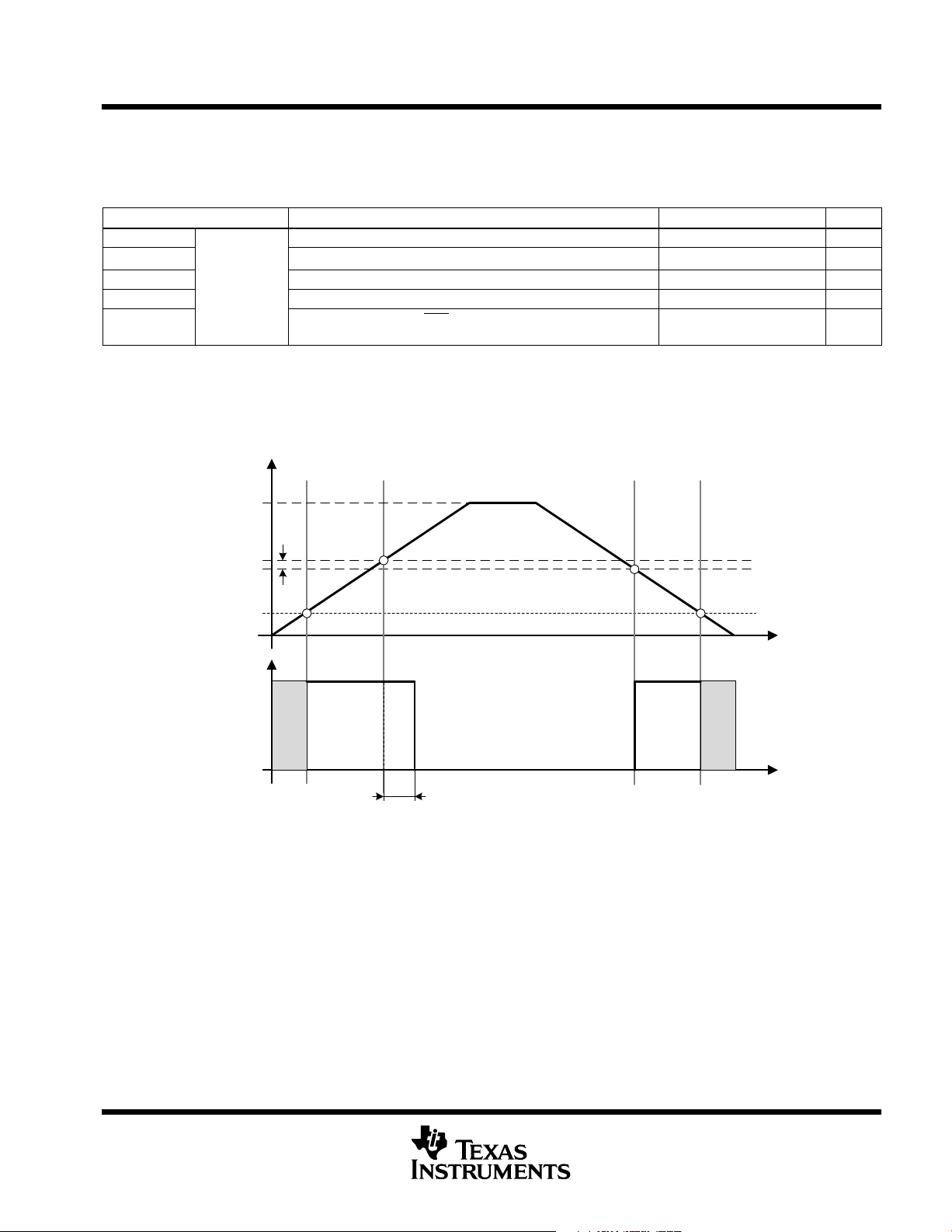
Timer_A capture timing TA0, TA1, TA2
Timer_A clock frequenc
externally applied to pin
Timer_A, clock frequency SMCLK or ACLK signal selected
Port P1, P2: P1.x to P2.x, external trigger signal
for the interrupt flag, (see Note 1)
TACLK, INCLK:
t
= t
(H)
(L)
NOTES: 1. The external signal sets the interrupt flag every time the minimum t
shorter than t
(int)
.
leakage current − Ports P1, P2, P5, and P6 (see Note 1)
PARAMETER TEST CONDITIONS MIN TYP MAX UNIT
I
lkg(Px.y)
NOTES: 1. The leakage current is measured with VSS or VCC applied to the corresponding pin(s), unless otherwise noted.
Leakage current
Port Px V
(see Note 2) VCC = 2.2 V/3 V ±50 nA
(Px.y)
2. The port pin must be selected as input.
VCC = 2.2 V 1.1 1.55
= 3 V 1.5 1.98
V
CC
VCC = 2.2 V 0.4 0.9
= 3 V 0.9 1.3
V
CC
VCC = 2.2 V 0.3 1.1
VCC = 3 V 0.5 1
CC
MIN TYP MAX UNIT
2.2 V 62
3 V 50
2.2 V 62
3 V 50
2.2 V 8
3 V 10
2.2 V 8
3 V 10
parameters are met. It may be set even with trigger signals
(int)
V
V
V
ns
ns
MHz
MHz
POST OFFICE BOX 655303 • DALLAS, TEXAS 75265
19

MSP430F42x0
,
P1.1/TA0/MCLK
MIXED SIGNAL MICROCONTROLLER
SLAS455D − MARCH 2005 − REVISED APRIL 2007
electrical characteristics over recommended operating free-air temperature (unless otherwise
noted) (continued)
outputs − Ports P1, P2, P5, and P6
PARAMETER TEST CONDITIONS MIN TYP MAX UNIT
V
High-level output voltage
OH
V
Low-level output voltage
OL
NOTES: 1. The maximum total current, I
specified voltage drop.
2. The maximum total current, I
specified voltage drop.
output frequency
PARAMETER TEST CONDITIONS MIN TYP MAX UNIT
f
(Px.y)
f
(MCLK)
t
(Xdc)
(x = 1, 2, 5, 6; 0 ≤ y ≤ 7)
P1.1/TA0/MCLK CL = 20 pF f
Duty cycle of output frequency
I
= −1.5 mA, V
OH(max)
I
= −6 mA, V
OH(max)
I
= −1.5 mA, V
OH(max)
I
= −6 mA, V
OH(max)
I
= 1.5 mA, V
OL(max)
I
= 6 mA, V
OL(max)
I
= 1.5 mA, V
OL(max)
I
= 6 mA, V
OL(max)
and I
OH(max)
and I
OH(max)
CL = 20 pF,
I
= ±1.5 mA
L
P1.1/TA0/MCLK
C
= 20 pF,
L
V
CC
OL(max),
OL(max),
= 2.2 V / 3 V
= 2.2 V, See Note 1 VCC−0.25 V
CC
= 2.2 V, See Note 2 VCC−0.6 V
CC
= 3 V, See Note 1 VCC−0.25 V
CC
= 3 V, See Note 2 VCC−0.6 V
CC
= 2.2 V, See Note 1 V
CC
= 2.2 V, See Note 2 V
CC
= 3 V, See Note 1 V
CC
= 3 V, See Note 2 V
CC
SS
SS
SS
SS
CC
CC
CC
CC
VSS+0.25
VSS+0.6
VSS+0.25
VSS+0.6
V
V
for all outputs combined, should not exceed ±12 mA to satisfy the maximum
for all outputs combined, should not exceed ±48 mA to satisfy the maximum
V
= 2.2 V / 3 V DC f
CC
f
= f
,
(MCLK)
f
(MCLK)
(XT1)
= f
(DCOCLK)
40% 60%
50%−
15 ns
50%
System
System
50%+
15 ns
MHz
MHz
20
POST OFFICE BOX 655303 • DALLAS, TEXAS 75265

MSP430F42x0
MIXED SIGNAL MICROCONTROLLER
SLAS455D − MARCH 2005 − REVISED APRIL 2007
electrical characteristics over recommended operating free-air temperature (unless otherwise
noted) (continued)
outputs − Ports P1, P2, P5, and P6 (continued)
TYPICAL LOW-LEVEL OUTPUT CURRENT
vs
LOW-LEVEL OUTPUT VOLTAGE
30
VCC = 2.2 V
P1.0
25
20
15
10
5
− Typical Low-level Output Current − mA
OL
I
0
0.0 0.5 1.0 1.5 2.0 2.5
VOL − Low-Level Output Voltage − V
TA = −40°C
TA = 25°C
TA = 85°C
Figure 2
TYPICAL LOW-LEVEL OUTPUT CURRENT
vs
LOW-LEVEL OUTPUT VOLTAGE
50
VCC = 3 V
45
P1.0
40
35
30
25
20
15
10
− Typical Low-level Output Current − mA
5
OL
I
0
0.0 0.5 1.0 1.5 2.0 2.5 3.0 3.5
VOL − Low-Level Output Voltage − V
TA = 25°C
TA = 85°C
Figure 3
TA = −40°C
TYPICAL HIGH-LEVEL OUTPUT CURRENT
vs
HIGH-LEVEL OUTPUT VOLTAGE
0
VCC = 2.2 V
P1.0
−5
−10
−15
TA = 85°C
−20
− Typical High-level Output Current − mA
OH
I
−25
0.0 0.5 1.0 1.5 2.0 2.5
VOH − High-Level Output Voltage − V
TA = −40°C
TA = 25°C
Figure 4
TYPICAL HIGH-LEVEL OUTPUT CURRENT
vs
HIGH-LEVEL OUTPUT VOLTAGE
0
VCC = 3 V
−5
P1.0
−10
−15
−20
−25
−30
−35
−40
− Typical High-level Output Current − mA
−45
OH
I
−50
0.0 0.5 1.0 1.5 2.0 2.5 3.0 3.5
VOH − High-Level Output Voltage − V
TA = −40°C
TA = 25°CTA = 85°C
Figure 5
POST OFFICE BOX 655303 • DALLAS, TEXAS 75265
21

MSP430F42x0
)
t
d(LPM3)
Delay time
V
CC
2.2 V/3 V
μs
MIXED SIGNAL MICROCONTROLLER
SLAS455D − MARCH 2005 − REVISED APRIL 2007
electrical characteristics over recommended operating free-air temperature (unless otherwise
noted) (continued)
wake-up LPM3
PARAMETER TEST CONDITIONS MIN TYP MAX UNIT
f = 1 MHz 6
t
d(LPM3
Delay time
f = 2 MHz
V
CC
= 2.2 V/3 V
f = 3 MHz
RAM
PARAMETER TEST CONDITIONS MIN TYP MAX UNIT
VRAMh CPU halted (see Note 1) 1.6 V
NOTE 1: This parameter defines the minimum supply voltage when the data in program memory RAM remain unchanged. No program execution
should take place during this supply voltage condition.
LCD_A
PARAMETER TEST CONDITIONS VCC MIN TYP MAX UNIT
V
CC(LCD)
C
LCD
I
CC(LCD)
f
LCD
V
LCD
V
LCD
V
LCD
V
LCD
V
LCD
V
LCD
V
LCD
V
LCD
V
LCD
V
LCD
V
LCD
V
LCD
V
LCD
V
LCD
V
LCD
V
LCD
R
LCD
Supply Voltage Range
Capacitor on LCDCAP (see Note 1)
Average Supply Current (see Note 2)
LCD frequency 1.1 kHz
LCD voltage VLCDx = 0000 VCC V
LCD voltage VLCDx = 0001 2.60 V
LCD voltage VLCDx = 0010 2.66 V
LCD voltage VLCDx = 0011 2.72 V
LCD voltage VLCDx = 0100 2.78 V
LCD voltage VLCDx = 0101 2.84 V
LCD voltage VLCDx = 0110 2.90 V
LCD voltage VLCDx = 0111 2.96 V
LCD voltage VLCDx = 1000 3.02 V
LCD voltage VLCDx = 1001 3.08 V
LCD voltage VLCDx = 1010 3.14 V
LCD voltage VLCDx = 1011 3.20 V
LCD voltage VLCDx = 1100 3.26 V
LCD voltage VLCDx = 1101 3.32 V
LCD voltage VLCDx = 1110 3.38 V
LCD voltage VLCDx = 1111 3.44 3.60 V
LCD Driver Output impedance
NOTES: 1. Enabling the internal charge pump with an external capacitor smaller than the minimum specified might damage the device.
2. Refer to the supply current specifications I
3. Connecting an actual display will increase the current consumption depending on the size of the LCD.
Charge pump enabled
(LCDCPEN = 1; VLCDx > 0000)
Charge pump enabled
(LCDCPEN = 1; VLCDx > 0000)
V
VLCDx= 1000, all segments on
f
no LCD connected (see Note 3)
T
V
VLCDx = 1000, I
(LPM3)
=3V; LCDCPEN = 1;
LCD(typ)
= f
LCD
= 25°C
A
LCD
/32
ACLK
= 3V; LCDCPEN = 1;
LOAD
= ±10μA
2.2 V 3.8 μA
2.2 V 10 kΩ
for additional current specifications with the LCD_A module active.
2.2 3.6 V
4.7 μF
6
μs
6
22
POST OFFICE BOX 655303 • DALLAS, TEXAS 75265
MSP430F42x0
MIXED SIGNAL MICROCONTROLLER
SLAS455D − MARCH 2005 − REVISED APRIL 2007
electrical characteristics over recommended operating free-air temperature (unless otherwise
noted) (continued)
POR/brownout reset (BOR) (see Note 1)
PARAMETER TEST CONDITIONS MIN TYP MAX UNIT
t
d(BOR)
V
CC(start)
V
(B_IT−)
V
hys(B_IT−)
t
(reset)
Brownout
(see Note 2)
dVCC/dt ≤ 3 V/s (see Figure 6) 0.7 × V
dVCC/dt ≤ 3 V/s (see Figure 6 through Figure 8) 1.71 V
dVCC/dt ≤ 3 V/s (see Figure 6) 70 130 180 mV
Pulse length needed at RST/NMI pin to accepted reset internally,
V
= 2.2 V/3 V
CC
2 μs
NOTES: 1. The current consumption of the brownout module is already included in the ICC current consumption data. The voltage level
V
+ V
(B_IT−)
hys(B_IT−)
2. During power up, the CPU begins code execution following a period of t
FLL+ settings must not be changed until V
is ≤ 1.8V.
CC
≥ V
CC(min)
, where V
after VCC = V
d(BOR)
is the minimum supply voltage for the desired
CC(min)
(B_IT−)
+ V
hys(B_IT−)
operating frequency. See the MSP430x4xx Family User’s Guide (SLAU056) for more information on the brownout.
typical characteristics
(B_IT−)
2000 μs
V
. The default
V
V
CC(start)
V
CC
(B_IT−)
1
0
V
hys(B_IT−)
t
d(BOR)
Figure 6. POR/Brownout Reset (BOR) vs Supply Voltage
POST OFFICE BOX 655303 • DALLAS, TEXAS 75265
23

MSP430F42x0
MIXED SIGNAL MICROCONTROLLER
SLAS455D − MARCH 2005 − REVISED APRIL 2007
electrical characteristics over recommended operating free-air temperature (unless otherwise
noted) (continued)
typical characteristics (continued)
− V
2
V
CC
Typical Conditions
1.5
1
= 3 V
V
3 V
CC
t
pw
CC(drop)
V
0.5
0
0.001 1 1000
tpw − Pulse Width − μs
Figure 7. V
2
VCC = 3 V
Typical Conditions
1.5
− V
1
CC(drop)
V
0.5
0
0.001 1 1000
Figure 8. V
(CC)min
CC(drop)
Level With a Square Voltage Drop to Generate a POR/Brownout Signal
t
− Pulse Width − μs
pw
Level With a Triangle Voltage Drop to Generate a POR/Brownout Signal
V
V
CC(drop)
CC(drop)
V
CC
3 V
1 ns 1 ns
tpw − Pulse Width − μs
t
pw
t
= t
f
r
t
f
tpw − Pulse Width − μs
t
r
24
POST OFFICE BOX 655303 • DALLAS, TEXAS 75265

MSP430F42x0
Step size between adjacent DCO taps:
(DCO)
Temperature drift, N
(DCO)
01Eh, FN_8=FN_4=FN_3=FN_2=0
MIXED SIGNAL MICROCONTROLLER
SLAS455D − MARCH 2005 − REVISED APRIL 2007
electrical characteristics over recommended operating free-air temperature (unless otherwise
noted)
DCO
PARAMETER TEST CONDITIONS V
N
=01Eh, FN_8=FN_4=FN_3=FN_2=0, D = 2; DCOPLUS= 0,
f
(DCOCLK)
f
(DCO=2)
f
(DCO=27)
f
(DCO=2)
f
(DCO=27)
f
(DCO=2)
f
(DCO=27)
f
(DCO=2)
f
(DCO=27)
f
(DCO=2)
f
(DCO=27)
S
n
D
t
D
V
(DCO)
f
= 32.768 kHz
Crystal
FN_8=FN_4=FN_3=FN_2=0 ; DCOPLUS = 1
FN_8=FN_4=FN_3=FN_2=0; DCOPLUS = 1
FN_8=FN_4=FN_3=0, FN_2=1; DCOPLUS = 1
FN_8=FN_4=FN_3=0, FN_2=1; DCOPLUS = 1
FN_8=FN_4=0, FN_3= 1, FN_2=x; DCOPLUS = 1
FN_8=FN_4=0, FN_3= 1, FN_2=x; DCOPLUS = 1
FN_8=0, FN_4= 1, FN_3= FN_2=x; DCOPLUS = 1
FN_8=0, FN_4=1, FN_3= FN_2=x; DCOPLUS = 1
FN_8=1, FN_4=FN_3=FN_2=x; DCOPLUS = 1
FN_8=1,FN_4=FN_3=FN_2=x; DCOPLUS = 1
Step size between adjacent DCO taps:
Sn = f
DCO(Tap n+1)
Temperature drift, N
/ f
DCO(Tap n)
(see Figure 10 for taps 21 to 27)
= 01Eh, FN_8=FN_4=FN_3=FN_2=0
=
D = 2; DCOPLUS = 0, (see Note 2)
Drift with VCC variation, N
= 01Eh, FN_8=FN_4=FN_3=FN_2=0
(DCO)
D = 2; DCOPLUS = 0
1 < TAP ≤ 20 1.06 1.11
CC
2.2 V/3 V 1 MHz
2.2 V 0.3 0.65 1.25
2.2 V 2.5 5.6 10.5
2.2 V 0.7 1.3 2.3
2.2 V 5.7 10.8 18
2.2 V 1.2 2 3
2.2 V 9 15.5 25
2.2 V 1.8 2.8 4.2
2.2 V 13.5 21.5 33
2.2 V 2.8 4.2 6.2
2.2 V 21 32 46
TAP = 27 1.07 1.17
2.2 V –0.2 –0.3 –0.4
MIN TYP MAX UNIT
3 V 0.3 0.7 1.3
3 V 2.7 6.1 11.3
3 V 0.8 1.5 2.5
3 V 6.5 12.1 20
3 V 1.3 2.2 3.5
3 V 10.3 17.9 28.5
3 V 2.1 3.4 5.2
3 V 16 26.6 41
3 V 4.2 6.3 9.2
3 V 30 46 70
3 V –0.2 –0.3 –0.4
0 5 15 %/V
MHz
MHz
MHz
MHz
MHz
MHz
MHz
MHz
MHz
MHz
%/_C
f
(DCO)
f
(DCO3V)
1.0
1.8 3.02.4 3.6
Figure 9. DCO Frequency vs Supply Voltage VCC and vs Ambient Temperature
f
(DCO)
f
(DCO205C)
POST OFFICE BOX 655303 • DALLAS, TEXAS 75265
1.0
20 6040 85
0−20−400
TA − °CVCC − V
25

MSP430F42x0
MIXED SIGNAL MICROCONTROLLER
SLAS455D − MARCH 2005 − REVISED APRIL 2007
electrical characteristics over recommended operating free-air temperature (unless otherwise
noted) (continued)
1.17
(DCO)
f
- Stepsize Ratio between DCO Taps
n
S
1.11
1.07
1.06
Max
Min
12720
DCO Tap
Figure 10. DCO Tap Step Size
Legend
Tolerance at Tap 27
DCO Frequency
Adjusted by Bits
29 to 25 in SCFI1 {N
Tolerance at Tap 2
{DCO}
}
26
FN_2=0
FN_3=0
FN_4=0
FN_8=0
Overlapping DCO Ranges:
Uninterrupted Frequency Range
FN_2=1
FN_3=0
FN_4=0
FN_8=0
FN_2=x
FN_3=1
FN_4=0
FN_8=0
FN_2=x
FN_3=x
FN_4=1
FN_8=0
FN_2=x
FN_3=x
FN_4=x
FN_8=1
Figure 11. Five Overlapping DCO Ranges Controlled by FN_x Bits
POST OFFICE BOX 655303 • DALLAS, TEXAS 75265

MSP430F42x0
Integrated input capacitance
Integrated output capacitance
MIXED SIGNAL MICROCONTROLLER
SLAS455D − MARCH 2005 − REVISED APRIL 2007
electrical characteristics over recommended operating free-air temperature (unless otherwise
noted)
crystal oscillator, LFXT1 oscillator (see Notes 1 and 2)
PARAMETER TEST CONDITIONS MIN TYP MAX UNIT
OSCCAPx = 0h, VCC = 2.2 V / 3 V 0
C
XIN
C
XOUT
V
IL
V
IH
NOTES: 1. The parasitic capacitance from the package and board may be estimated to be 2 pF. The effective load capacitor for the crystal is
Integrated input capacitance
(see Note 4)
Integrated output capacitance
(see Note 4)
Input levels at XIN VCC = 2.2 V/3 V (see Note 3)
(C
XINxCXOUT
2. To improve EMI on the low-power LFXT1 oscillator, particularly in the LF mode (32 kHz), the following guidelines should be observed.
) / (C
XIN
+ C
OSCCAPx = 1h, V
OSCCAPx = 2h, V
OSCCAPx = 3h, VCC = 2.2 V / 3 V 18
OSCCAPx = 0h, VCC = 2.2 V / 3 V 0
OSCCAPx = 1h, V
OSCCAPx = 2h, V
OSCCAPx = 3h, VCC = 2.2 V / 3 V 18
). This is independent of XTS_FLL.
XOUT
− Keep as short of a trace as possible between the ’F42x0 and the crystal.
− Design a good ground plane around the oscillator pins.
− Prevent crosstalk from other clock or data lines into oscillator pins XIN and XOUT.
− Avoid running PCB traces underneath or adjacent to the XIN and XOUT pins.
− Use assembly materials and praxis to avoid any parasitic load on the oscillator XIN and XOUT pins.
− If conformal coating is used, ensure that it does not induce capacitive/resistive leakage between the oscillator pins.
− Do not route the XOUT line to the JTAG header to support the serial programming adapter as shown in other
documentation. This signal is no longer required for the serial programming adapter.
3. Applies only when using an external logic-level clock source. XTS_FLL must be set. Not applicable when using a crystal or
resonator.
4. External capacitance is recommended for precision real-time clock applications; OSCCAPx = 0h.
= 2.2 V / 3 V 10
CC
= 2.2 V / 3 V 14
CC
= 2.2 V / 3 V 10
CC
= 2.2 V / 3 V 14
CC
V
SS
0.8×V
CC
0.2×V
V
CC
CC
pF
pF
V
POST OFFICE BOX 655303 • DALLAS, TEXAS 75265
27

MSP430F42x0
SD16LP
f
SD16
MHz,
SD16LP
f
SD16
MHz,
Differential full scale
Differential input
performance
(see Note 1)
f
SD16
1MHz,
f
SD16
1MHz,
Absolute input
Common mode
MIXED SIGNAL MICROCONTROLLER
SLAS455D − MARCH 2005 − REVISED APRIL 2007
electrical characteristics over recommended operating free-air temperature (unless otherwise
noted) (continued)
SD16_A, power supply and recommended operating conditions
AV
I
SD16
f
SD16
PARAMETER TEST CONDITIONS V
CC
Analog supply
voltage
Analog supply
current including
internal reference
Analog front-end
AVCC = DV
CC
AVSS = DVSS = 0V
=
SD16
= 0,
= 1 MHz,
1
f
SD16OSR = 256
SD16LP = 1,
f
= 0.5 MHz,
SD16
SD16OSR = 256
=
SD16
= 0,
= 1 MHz,
1
f
SD16OSR = 256
SD16BUFx = 00; GAIN: 1,2 3 V 650 950
SD16BUFx = 00; GAIN: 4,8,16 3 V 730 1100
SD16BUFx = 00; GAIN: 32 3 V 1050 1550
SD16BUFx = 00; GAIN: 1 3 V 620 930
SD16BUFx = 00; GAIN: 32 3 V 700 1060
SD16BUFx = 01; GAIN: 1 3 V 850
SD16BUFx = 10; GAIN: 1 3 V 1130
SD16BUFx = 11; GAIN: 1 3 V 1130
SD16LP = 0 (Low power mode disabled) 3 V 0.03 1 1.1
input clock
frequency
SD16LP = 1 (Low power mode enabled) 3 V 0.03 0.5
CC
MIN TYP MAX UNIT
2.5 3.6 V
μA
MHz
SD16_A, input range
PARAMETER TEST CONDITIONS V
V
ID,FSR
Differential full scale
input voltage range
Differential input
voltage range for
V
ID
specified
(see Note 1)
Input impedance
Z
I
(one input pin
)
to AV
SS
Differential
Z
ID
Input impedance
(IN+ to IN−)
V
I
V
IC
Absolute input
voltage range
Common-mode
input voltage range
NOTES: 1. The analog input range depends on the reference voltage applied to V
is defined by V
V
or V
FSR+
FSR+
FSR−
Bipolar Mode, SD16UNI = 0 −V
Unipolar Mode, SD16UNI = 1 0 +V
SD16GAINx = 1 ±500
SD16GAINx = 2 ±250
SD16REFON=1
SD16GAINx = 4 ±125
SD16GAINx = 8 ±62
SD16GAINx = 16 ±31
SD16GAINx = 32 ±15
f
= 1MHz,
SD16
SD16BUFx = 00
f
= 1MHz,
SD16
SD16BUFx = 01
f
= 1MHz,
SD16
SD16BUFx = 00
f
= 1MHz,
SD16
SD16BUFx > 00
SD16GAINx = 1 3 V 200
SD16GAINx = 32 3 V 75
SD16GAINx = 1 3 V >10 MΩ
SD16GAINx = 1 3 V 300 400
SD16GAINx = 32 3 V 100 150
SD16GAINx = 1 3 V >10 MΩ
SD16BUFx = 00 AV
SD16BUFx > 00 AV
SD16BUFx = 00 AV
SD16BUFx > 00 AV
= +(V
/2)/GAIN and V
REF
FSR−
= −(V
/2)/GAIN. The analog input range should not exceed 80% of
REF
.
CC
REF
MIN TYP MAX UNIT
/2GAIN +V
REF
-0.1V AV
SS
SS
-0.1V AV
SS
SS
. If V
is sourced externally, the full-scale range
REF
REF
REF
AV
AV
CC
CC
/2GAIN mV
/2GAIN mV
mV
kΩ
kΩ
CC
CC
V
V
−1.2V
−1.2V
28
POST OFFICE BOX 655303 • DALLAS, TEXAS 75265

MSP430F42x0
distortion ratio
Signal to noise +
f
IN
50Hz
ppm
Common mode
MIXED SIGNAL MICROCONTROLLER
SLAS455D − MARCH 2005 − REVISED APRIL 2007
electrical characteristics over recommended operating free-air temperature (unless otherwise
noted) (continued)
SD16_A, performance (f
PARAMETER TEST CONDITIONS V
SINAD
dG/dT
dG/dV
CC
NOTES: 1. Calculated using the box method: (MAX(−40...85_C) − MIN(−40...85_C))/MIN(−40...85_C)/(85C − (−40_C))
Signal-to-noise +
distortion ratio
Nominal gain SD16GAINx = 1; SD16OSRx = 1024 3 V 0.97 1.00 1.02
Gain temperature
drift
Gain supply voltage
drift
2. Calculated using the box method: (MAX(2.5...3.6V) − MIN(2.5...3.6V))/MIN(2.5...3.6V)/(3.6V − 2.5V)
SD16_A, performance (f
PARAMETER TEST CONDITIONS V
SINAD
G
E
OS
dEOS/dT
CMRR
AC PSRR
Signal-to-noise +
distortion ratio
Nominal gain
Offset error
Offset error
temperature
coefficient
Common-mode
rejection ratio
AC power supply
rejection ratio
= 30kHz, SD16REFON = 1, SD16BUFx = 01)
SD16
MIN TYP MAX UNIT
CC
SD16GAINx = 1,Signal Amplitude = 500mV
SD16OSRx = 256
SD16GAINx = 1,Signal Amplitude = 500mV
SD16OSRx = 512
SD16GAINx = 1,Signal Amplitude = 500mV
SD16OSRx = 1024
SD16GAINx = 1; SD16OSRx = 1024 (see Note 1) 3 V 15 ppm/_C
SD16GAINx = 1; SD16OSRx = 1024; VCC = 2.5V - 3.6V
(see Note 2)
= 1MHz, SD16OSRx = 256, SD16REFON = 1, SD16BUFx = 00)
SD16
SD16GAINx = 1,Signal Amplitude = 500mV 3 V 83.5 85
SD16GAINx = 2,Signal Amplitude = 250mV 3 V 81.5 84
SD16GAINx = 4,Signal Amplitude = 125mV
SD16GAINx = 8,Signal Amplitude = 62mV
SD16GAINx = 16,Signal Amplitude = 31mV 3 V 69 73
SD16GAINx = 32,Signal Amplitude = 15mV 3 V 62 69
SD16GAINx = 1 3 V 0.97 1.00 1.02
SD16GAINx = 2 3 V 1.90 1.96 2.02
SD16GAINx = 4 3 V 3.76 3.86 3.96
SD16GAINx = 8 3 V 7.36 7.62 7.84
SD16GAINx = 16 3 V 14.56 15.04 15.52
SD16GAINx = 32 3 V 27.20 28.35 29.76
SD16GAINx = 1 3 V ±0.2
SD16GAINx = 32 3 V ±1.5
SD16GAINx = 1 3 V ±4 ±20
SD16GAINx = 32 3 V ±20 ±100
SD16GAINx = 1, Common-mode input signal:
V
= 500 mV, fIN = 50 Hz, 100 Hz
ID
SD16GAINx = 32, Common-mode input signal:
V
= 16 mV, fIN = 50 Hz, 100 Hz
ID
SD16GAINx = 1, VCC = 3 V ± 100 mV, f
fIN = 2.8Hz
fIN = 50Hz,
=
100Hz
= 50 Hz 3 V >80 dB
VCC
3 V 84
3 V 84
3 V 84
MIN TYP MAX UNIT
CC
3 V 76 79.5
,
3 V 73 76.5
3 V >90
3 V >75
0.35 %/V
dB
dB
%FSR
ppm
FSR/_C
dB
POST OFFICE BOX 655303 • DALLAS, TEXAS 75265
29

MSP430F42x0
V
Sensor
(
2)
mV
MIXED SIGNAL MICROCONTROLLER
SLAS455D − MARCH 2005 − REVISED APRIL 2007
electrical characteristics over recommended operating free-air temperature (unless otherwise
noted) (continued)
SD16_A, temperature sensor
PARAMETER TEST CONDITIONS V
TC
Sensor
V
Offset,sensor
Sensor temperature
coefficient
Sensor offset voltage −100 100 mV
Temperature sensor voltage at TA = 85°C 3 V 435 475 515
V
Sensor
Sensor output voltage
see Note
Temperature sensor voltage at TA = 25°C 3 V 355 395 435
Temperature sensor voltage at TA = 0°C 3 V 320 360 400
NOTES: 1. The following formula can be used to calculate the temperature sensor output voltage:
V
Sensor,typ
2. Results based on characterization and/or production test, not TC
= TC
( 273 + T [°C] ) + V
Sensor
Offset,sensor
[mV]
Sensor
or V
Offset,sensor
SD16_A, built-in voltage reference
PARAMETER TEST CONDITIONS V
V
REF
I
REF
TC Temperature coefficient SD16REFON = 1, SD16VMIDON = 0 3 V 18 50 ppm/K
C
REF
I
LOAD
t
ON
DC PSR
NOTES: 1. There is no capacitance required on V
Internal reference
voltage
Reference supply
current
V
load capacitance SD16REFON = 1, SD16VMIDON = 0 (see Note 1) 100 nF
REF
V
maximum load
REF(I)
current
Turn on time
DC power supply
rejection, ΔV
REF
/ΔV
SD16REFON = 1, SD16VMIDON = 0 3 V 1.14 1.20 1.26 V
SD16REFON = 1, SD16VMIDON = 0 3 V 175 260 μA
SD16REFON = 1, SD16VMIDON = 0 3 V ±200 nA
SD16REFON = 0−>1, SD16VMIDON = 0,
C
= 100nF
REF
SD16REFON = 1, SD16VMIDON = 0, VCC = 2.5 V to 3.6 V 100 uV/V
CC
. However, a capacitance of at least 100nF is recommended to reduce any reference
REF
voltage noise.
MIN TYP MAX UNIT
CC
1.18 1.32 1.46 mV/K
.
MIN TYP MAX UNIT
CC
3 V 5 ms
mV
SD16_A, reference output buffer
PARAMETER TEST CONDITIONS V
V
REF,BUF
I
REF,BUF
C
REF(O)
I
LOAD,Max
t
ON
Reference buffer output
voltage
Reference Supply +
Reference output buffer
quiescent current
Required load
capacitance on V
REF
Maximum load current
on V
REF
Maximum voltage variation vs. load current
Turn on time
MIN TYP MAX UNIT
CC
SD16REFON = 1, SD16VMIDON = 1 3 V 1.2 V
SD16REFON = 1, SD16VMIDON = 1 3 V 385 600 μA
SD16REFON = 1, SD16VMIDON = 1 470 nF
SD16REFON = 1, SD16VMIDON = 1 3 V ±1 mA
|I
| = 0 to 1mA 3 V −15 +15 mV
LOAD
SD16REFON = 0−>1; SD16VMIDON = 1;
C
= 470nF
REF
3 V 100 μs
30
POST OFFICE BOX 655303 • DALLAS, TEXAS 75265

SD16_A, external reference input
PARAMETER TEST CONDITIONS V
V
REF(I)
I
REF(I)
Input voltage range SD16REFON = 0 3 V 1.0 1.25 1.5 V
Input current SD16REFON = 0 3 V 50 nA
MSP430F42x0
MIXED SIGNAL MICROCONTROLLER
SLAS455D − MARCH 2005 − REVISED APRIL 2007
MIN TYP MAX UNIT
CC
POST OFFICE BOX 655303 • DALLAS, TEXAS 75265
31

MSP430F42x0
Supply Current
MIXED SIGNAL MICROCONTROLLER
SLAS455D − MARCH 2005 − REVISED APRIL 2007
electrical characteristics over recommended operating free-air temperature (unless otherwise
noted) (continued)
12-bit DAC, supply specifications
AV
CC
I
DD
PSRR
PARAMETER TEST CONDITIONS V
AV
DVCC,
Analog supply voltage
CC =
= DVSS =0 V
AV
SS
DAC12AMPx=2, DAC12IR=0,
DAC12_xDAT=0800h
DAC12AMPx=2, DAC12IR=1,
Supply Current
(see Notes 1 and 2)
DAC12_xDAT=0800h, V
REF,DAC12
DAC12AMPx=5, DAC12IR=1,
DAC12_xDAT=0800h, V
REF,DAC12
= AV
= AV
CC
CC
DAC12AMPx=7, DAC12IR=1,
= AV
= 1.2V
CC
Power supply
rejection ratio
(see Notes 3 and 4)
DAC12_xDAT=0800h, V
DAC12_xDAT = 800h, V
= 100mV
ΔAV
CC
REF,DAC12
REF,DAC12
CC
2.2V/3V 50 11 0
2.2V/3V 50 11 0
2.2V/3V 200 440
2.2V/3V 700 1500
2.7V 70 dB
NOTES: 1. No load at the output pin assuming that the control bits for the shared pins are set properly.
2. Current into reference terminals not included. If DAC12IR = 1 current flows through the input divider; see Reference Input
specifications.
3. PSRR = 20*log{ΔAV
4. V
is applied externally. The internal reference is not used.
REF
CC
/ΔV
DAC12_xOUT
}.
MIN TYP MAX UNIT
2.20 3.60 V
μA
32
POST OFFICE BOX 655303 • DALLAS, TEXAS 75265

MSP430F42x0
t
Offset_Cal
ms
MIXED SIGNAL MICROCONTROLLER
SLAS455D − MARCH 2005 − REVISED APRIL 2007
electrical characteristics over recommended operating free-air temperature (unless otherwise
noted) (continued)
12-bit DAC, linearity specifications (see Figure 12)
PARAMETER TEST CONDITIONS V
CC
Resolution (12-bit Monotonic) 12 bits
INL
DNL
E
O
d
E(O)/dT
Integral nonlinearity
(see Note 1)
Differential nonlinearity
(see Note 1)
Offset voltage w/o
calibration
(see Notes 1, 2)
Offset voltage with
calibration
(see Notes 1, 2)
Offset error
temperature coefficient
V
REF,DAC12
DAC12AMPx = 7, DAC12IR = 1
V
REF,DAC12
DAC12AMPx = 7, DAC12IR = 1
V
REF,DAC12
DAC12AMPx = 7, DAC12IR = 1
V
REF,DAC12
DAC12AMPx = 7, DAC12IR = 1
= 1.2V
= 1.2V
= 1.2V
= 1.2V
2.7V ±2.0 ±8.0 LSB
2.7V ±0.4 ±1.0 LSB
2.7V ±20
2.7V ±2.5
2.7V ±30 μV/C
(see Note 1)
E
G
d
E(G)/dT
t
Offset_Cal
Gain error (see Note 1) V
Gain temperature
coefficient (see Note 1)
Time for offset calibration
(see Note 3)
REF,DAC12
= 1.2V 2.7V ±3.50 % FSR
2.7V 10
DAC12AMPx=2 2.7V 100
DAC12AMPx=3,5 2.7V 32
DAC12AMPx=4,6,7 2.7V 6
NOTES: 1. Parameters calculated from the best-fit curve from 0x0A to 0xFFF. The best-fit curve method is used to deliver coefficients “a” and
“b” of the first order equation: y = a + b*x. V
DAC12_xOUT
= EO + (1 + EG) * (V
REF,DAC12
/4095) * DAC12_xDAT, DAC12IR = 1.
2. The offset calibration works on the output operational amplifier. Offset Calibration is triggered setting bit DAC12CALON
3. The offset calibration can be done if DAC12AMPx = {2, 3, 4, 5, 6, 7}. The output operational amplifier is switched off with
DAC12AMPx ={0, 1}. It is recommended that the DAC12 module be configured prior to initiating calibration. Port activity during
calibration may effect accuracy and is not recommended.
MIN TYP MAX UNIT
mV
ppm of
FSR/°C
ms
DAC Output
DAC V
OUT
V
R
Load
=
AV
CC
R+
Ideal transfer
function
2
C
Load
= 100pF
Offset Error
Positive
Negative
Gain Error
DAC Code
Figure 12. Linearity Test Load Conditions and Gain/Offset Definition
POST OFFICE BOX 655303 • DALLAS, TEXAS 75265
33

MSP430F42x0
MIXED SIGNAL MICROCONTROLLER
SLAS455D − MARCH 2005 − REVISED APRIL 2007
electrical characteristics over recommended operating free-air temperature (unless otherwise
noted) (continued)
12-bit DAC, linearity specifications (continued)
TYPICAL INL ERROR
vs
DIGITAL INPUT DATA
4
VCC = 2.2 V, V
DAC12AMPx = 7
3
DAC12IR = 1
2
1
0
−1
REF
= 1.2V
−2
INL − Integral Nonlinearity Error − LSB
−3
−4
0 512 1024 1536 2048 2560 3072 3584
DAC12_xDAT − Digital Code
TYPICAL DNL ERROR
vs
DIGITAL INPUT DATA
2.0
1.5
1.0
0.5
0.0
−0.5
−1.0
VCC = 2.2 V, V
DAC12AMPx = 7
DAC12IR = 1
REF
= 1.2V
4095
−1.5
DNL − Differential Nonlinearity Error − LSB
−2.0
0 512 1024 1536 2048 2560 3072 3584
34
4095
DAC12_xDAT − Digital Code
POST OFFICE BOX 655303 • DALLAS, TEXAS 75265

MSP430F42x0
range
Max DAC12
(see Figure 15)
MIXED SIGNAL MICROCONTROLLER
SLAS455D − MARCH 2005 − REVISED APRIL 2007
electrical characteristics over recommended operating free-air temperature (unless otherwise
noted) (continued)
12-bit DAC, output specifications
PARAMETER TEST CONDITIONS V
No Load, V
REF,DAC12
= AVCC,
DAC12_xDAT = 0h, DAC12IR = 1,
DAC12AMPx = 7
No Load, V
Output voltage
V
O
range
(see Note 1,
Figure 15)
DAC12_xDAT = 0FFFh, DAC12IR = 1,
DAC12AMPx = 7
R
Load
DAC12_xDAT = 0h, DAC12IR = 1,
REF,DAC12
= 3 kΩ, V
= AVCC,
REF,DAC12
= AVCC,
DAC12AMPx = 7
R
Load
= 3 kΩ, V
REF,DAC12
= AVCC,
DAC12_xDAT = 0FFFh, DAC12IR = 1,
DAC12AMPx = 7
C
L(DAC12)
I
L(DAC12)
Max DAC12
load capacitance
Max DAC12
load current
2.2V/3V 100 pF
R
Load
= 3 kΩ, V
O/P(DAC12)
< 0.3 V,
DAC12AMPx = 2, DAC12_xDAT = 0h
= 3 kΩ,
R
Load
V
O/P(DAC12)
> AVCC−0.3 V
DAC12_xDAT = 0FFFh
R
= 3 kΩ,
Load
0.3V ≤ V
O/P(DAC12)
≤ AVCC − 0.3V
R
O/P(DAC12)
Output
Resistance
(see Figure 15)
NOTES: 1. Data is valid after the offset calibration of the output amplifier.
R
C
Load
Load
= 100pF
AV
CC
2
DAC12
I
Load
O/P(DAC12_x)
Figure 15. DAC12_x Output Resistance Tests
CC
2.2V/3V 0 0.005
2.2V/3V AVCC−0.05 AV
2.2V/3V 0 0.1
2.2V/3V AVCC−0.13 AV
2.2V −0.5 +0.5
3V −1.0 +1.0
2.2V/3V 150 250
2.2V/3V 150 250
2.2V/3V 1 4
R
O/P(DAC12_x)
Max
Min
MIN TYP MAX UNIT
CC
CC
0.3
AVCC −0.3V
AV
CC
V
mA
Ω
V
OUT
POST OFFICE BOX 655303 • DALLAS, TEXAS 75265
35

MSP430F42x0
Reference input
Reference input
DAC12_xDAT = 800h
t
ON
Error
V(O)
±0.5 LSB
μs
)
t
S(FS)
μs
)
DAC12_xDAT =
t
S(C-C)
3F8h→ 408h→ 3F8h
μs
SR
Slew Rate
V/μs
Glitch energy: full scale
nV s
MIXED SIGNAL MICROCONTROLLER
SLAS455D − MARCH 2005 − REVISED APRIL 2007
electrical characteristics over recommended operating free-air temperature (unless otherwise
noted)
12-bit DAC, reference input specifications
V
REF
Ri
PARAMETER TEST CONDITIONS V
DAC12IR=0, (see Notes 1 and 2) 2.2V/3V AVCC/3 AVCC+0.2
DAC12IR=1, (see Notes 3 and 4)
DAC12IR=0 2.2V/3V 20 MΩ
DAC12IR=1 2.2V/3V 40 48 56 kΩ
(VREF)
Reference input
voltage range
Reference input
resistance
CC
2.2V/3V AV
NOTES: 1. For a full-scale output, the reference input voltage can be as high as 1/3 of the maximum output voltage swing (AVCC).
2. The maximum voltage applied at reference input voltage terminal V
= [AVCC − V
REF
3. For a full-scale output, the reference input voltage can be as high as the maximum output voltage swing (AV
4. The maximum voltage applied at reference input voltage terminal V
12-bit DAC, dynamic specifications; V
REF,DAC12
= AVCC, DAC12IR = 1 (see Figure 16 and Figure 17)
= [AVCC − V
REF
PARAMETER TEST CONDITIONS V
t
ON
t
S(FS
t
S(C-C
DAC12 ontime
Settling
time,full-scale 80h→ F7Fh→ 80h
Settling time,
code to code
SR Slew Rate
Glitch energy: full-scale
NOTES: 1. R
Load
and C
DAC12_xDAT = 800h,
< ±0.5 LSB
V(O)
<
Error
(see Note 1,Figure 16)
DAC12_xDAT =
DAC12_xDAT =
3F8h→ 408h→ 3F8h
BF8h→ C08h→ BF8h
DAC12_xDAT =
80h→ F7Fh→ 80h
DAC12_xDAT =
80h→ F7Fh→ 80h
connected to AVSS (not AVCC/2) in Figure 16.
Load
DAC12AMPx=0 → {2, 3, 4} 2.2V/3V 60 120
,
DAC12AMPx=0 → {5, 6} 2.2V/3V 15 30
DAC12AMPx=0 → 7 2.2V/3V 6 12
DAC12AMPx=2 2.2V/3V 100 200
DAC12AMPx=3,5 2.2V/3V 40 80
DAC12AMPx=4,6,7 2.2V/3V 15 30
DAC12AMPx=2 2.2V/3V 5
DAC12AMPx=3,5 2.2V/3V 2
DAC12AMPx=4,6,7 2.2V/3V 1
DAC12AMPx=2 2.2V/3V 0.05 0.12
DAC12AMPx=3,5 2.2V/3V 0.35 0.7
DAC12AMPx=4,6,7 2.2V/3V 1.5 2.7
DAC12AMPx=2 2.2V/3V 10
DAC12AMPx=3,5 2.2V/3V 10
DAC12AMPx=4,6,7 2.2V/3V 15
2. Slew rate applies to output voltage steps ≥ 200mV.
MIN TYP MAX UNIT
CC
+0.2
).
] / [3*(1 + EG)].
E(O)
] / (1 + EG).
E(O)
CC
CCAVCC
MIN TYP MAX UNIT
V
μs
μs
μs
V/μs
nV-s
36
DAC Output
R
O/P(DAC12.x)
Conversion 1 Conversion 2
V
I
Load
R
Load
= 3 kΩ
AV
OUT
CC
Glitch
Energy
2
C
= 100pF
Load
t
Figure 16. Settling Time and Glitch Energy Testing
POST OFFICE BOX 655303 • DALLAS, TEXAS 75265
+/− 1/2 LSB
settleLH
Conversion 3
+/− 1/2 LSB
t
settleHL
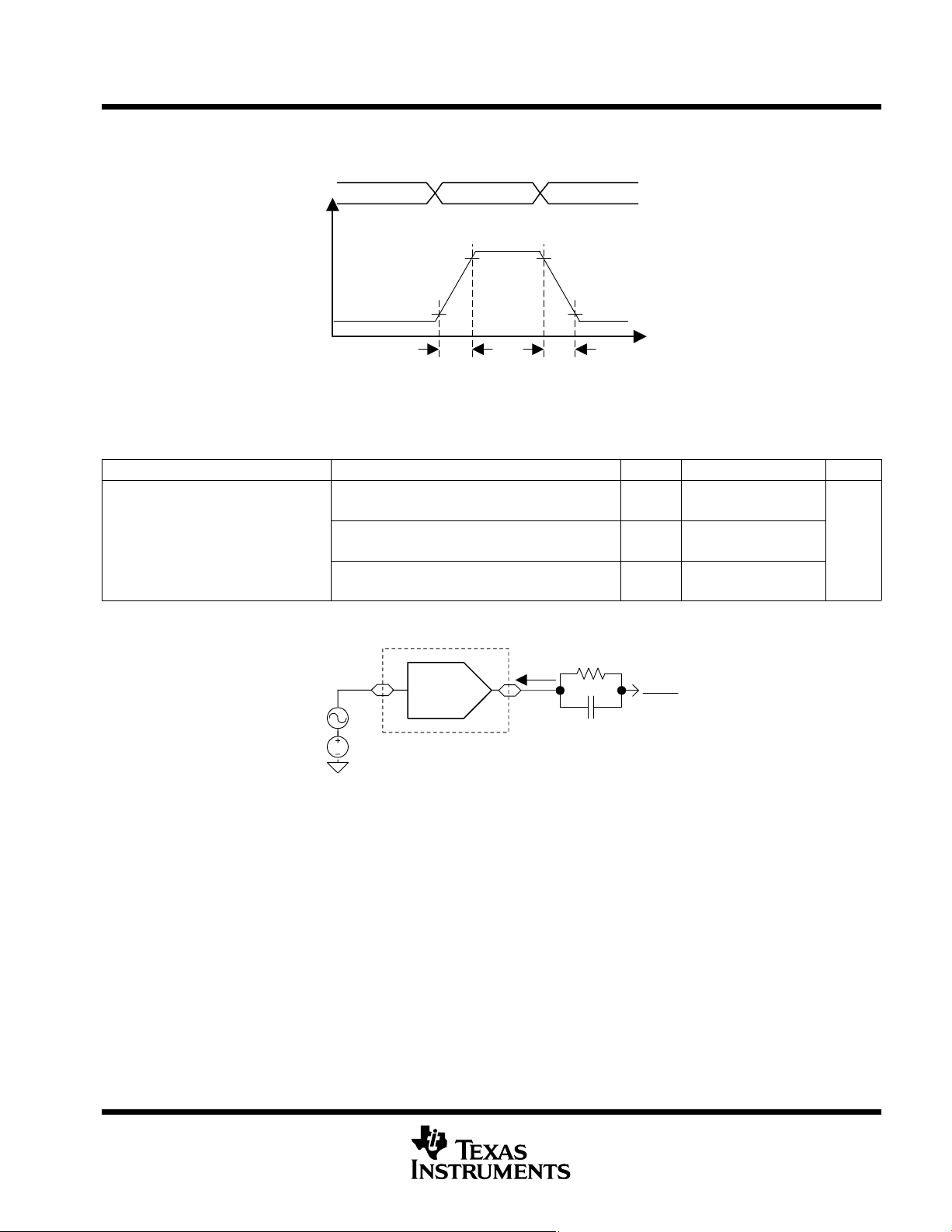
MSP430F42x0
MIXED SIGNAL MICROCONTROLLER
SLAS455D − MARCH 2005 − REVISED APRIL 2007
electrical characteristics over recommended operating free-air temperature (unless otherwise
noted)
Conversion 1 Conversion 2
V
OUT
90%
10%
t
Figure 17. Slew Rate Testing
12-bit DAC, dynamic specifications continued (T
PARAMETER TEST CONDITIONS V
DAC12AMPx = {2, 3, 4}, DAC12SREFx = 2,
DAC12IR = 1, DAC12_xDAT = 800h
DAC12AMPx = {5, 6}, DAC12SREFx = 2,
PP
DAC12IR = 1, DAC12_xDAT = 800h
DAC12AMPx = 7, DAC12SREFx = 2,
DAC12IR = 1, DAC12_xDAT = 800h
= 100 pF
BW
−3dB
NOTES: 1. R
3-dB bandwidth,
=1.5V, VAC=0.1V
V
DC
(see Figure 18)
= 3 kΩ, C
LOAD
LOAD
Conversion 3
90%
10%
SRLH
= 25°C unless otherwise noted)
A
t
SRHL
CC
2.2V/3V 40
2.2V/3V 180
2.2V/3V 550
MIN TYP MAX UNIT
kHz
= 3 kΩ
R
Load
I
Load
DACx
C
Load
= 100pF
AV
CC
2
AC
DC
Ve
REF+
DAC12_x
Figure 18. Test Conditions for 3-dB Bandwidth Specification
POST OFFICE BOX 655303 • DALLAS, TEXAS 75265
37
MSP430F42x0
MIXED SIGNAL MICROCONTROLLER
SLAS455D − MARCH 2005 − REVISED APRIL 2007
electrical characteristics over recommended operating free-air temperature (unless otherwise
noted)
Flash Memory
PARAMETER
V
CC(PGM/
ERASE)
f
FTG
I
PGM
I
ERASE
t
CPT
t
CMErase
Program and Erase supply voltage 2.5 3.6 V
Flash Timing Generator frequency 257 476 kHz
Supply current from DVCC during program 2.5V/3.6V 3 5 mA
Supply current from DVCC during erase 2.5V/3.6V 3 7 mA
Cumulative program time see Note 1 2.5V/3.6V 10 ms
Cumulative mass erase time see Note 2 2.5V/3.6V 200 ms
Program/Erase endurance 10
t
Retention
t
Word
t
Block, 0
t
Block, 1-63
t
Block, End
t
Mass Erase
t
Seg Erase
Data retention duration TJ = 25°C 100 years
Word or byte program time 35
Block program time for 1st byte or word 30
Block program time for each additional byte or word
Block program end-sequence wait time
Mass erase time 5297
Segment erase time 4819
NOTES: 1. The cumulative program time must not be exceeded when writing to a 64−byte flash block. This parameter applies to all programming
methods: individual word/byte write and block write modes.
2. The mass erase duration generated by the flash timing generator is at least 11.1ms ( = 5297x1/f
achieve the required cumulative mass erase time the Flash Controller’s mass erase operation can be repeated until this time is met.
(A worst case minimum of 19 cycles are required).
3. These values are hardwired into the Flash Controller’s state machine (t
TEST
CONDITIONS
see Note 3
FTG
= 1/f
FTG
V
CC
MIN NOM MAX UNIT
4
5
10
21
6
,max = 5297x1/476kHz). To
FTG
cycles
t
FTG
).
JTAG Interface
TEST
CONDITIONS
V
CC
MIN NOM MAX UNIT
2.2 V 0 5 MHz
3 V 0 10 MHz
f
TCK
R
Internal
NOTES: 1. f
2. TMS, TDI/TCLK, and TCK pull-up resistors are implemented in all versions.
PARAMETER
TCK input frequency see Note 1
Internal pull-up resistance on TMS, TCK, TDI/TCLK see Note 2 2.2 V/ 3 V 25 60 90 kΩ
may be restricted to meet the timing requirements of the module selected.
TCK
JTAG Fuse (see Note 1)
PARAMETER
V
CC(FB)
V
FB
I
FB
t
FB
Supply voltage during fuse-blow condition TA = 25°C 2.5 V
Voltage level on TDI/TCLK for fuse-blow: F versions 6 7 V
Supply current into TDI/TCLK during fuse blow 100 mA
Time to blow fuse 1 ms
NOTES: 1. Once the fuse is blown, no further access to the MSP430 JTAG/Test and emulation features is possible. The JTAG block is switched
to bypass mode.
TEST
CONDITIONS
V
CC
MIN NOM MAX UNIT
38
POST OFFICE BOX 655303 • DALLAS, TEXAS 75265

MIXED SIGNAL MICROCONTROLLER
SLAS455D − MARCH 2005 − REVISED APRIL 2007
input/output schematics
Port P1 pin schematic: P1.0, P1.1, input/output with Schmitt−trigger
Pad Logic
DV
SS
DV
SS
DV
SS
MSP430F42x0
P1DIR.x
P1OUT.x
Module X OUT
P1SEL.x
P1IN.x
Module X IN
P1IRQ.x
Note: x = 0,1
0
1
0
1
P1SEL.x
P1IES.x
EN
D
P1IE.x
P1IFG.x
Direction
0: Input
1: Output
EN
Q
Set
Interrupt
Edge
Select
Bus
Keeper
EN
P1.0/TA0
P1.1/TA0/MCLK
Port P1 (P1.0, P1.1) pin functions
PIN NAME (P1.X)
P1.0/TA0 0
P1.1/TA0/MCLK 1
†
Default after reset (PUC/POR)
NOTES: 1. N/A: Not available or not applicable.
2. X: Don’t care.
X FUNCTION
P1.0† Input/Output 0/1 0
Timer_A3.CCI0A 0 1
Timer_A3.TA0 1 1
P1.1† Input/Output 0/1 0
Timer_A3.CCI0B 0 1
MCLK 1 1
POST OFFICE BOX 655303 • DALLAS, TEXAS 75265
CONTROL BITS / SIGNALS
P1DIR.x P1SEL.x
39

MSP430F42x0
MIXED SIGNAL MICROCONTROLLER
SLAS455D − MARCH 2005 − REVISED APRIL 2007
Port P1 pin schematic: P1.2, input/output with Schmitt−trigger and analog functions
INCH=4
SD16AE.x
P1DIR.x
P1OUT.x
Module X OUT
P1SEL.x
P1IN.x
Module X IN
P1IRQ.x
A4−
Pad Logic
0
AV
SS
1
0
1
0
1
EN
D
P1IE.x
P1IFG.x
Direction
0: Input
1: Output
P1.2/TA1/A4−
Bus
Keeper
EN
EN
Q
Set
P1SEL.x
P1IES.x
Note: x = 2
Interrupt
Edge
Select
Port P1 (P1.2) pin functions
PIN NAME (P1.X)
P1.2/TA1/A4− 2
†
Default after reset (PUC/POR)
NOTES: 1. N/A: Not available or not applicable.
2. X: Don’t care.
3. Setting the SD16AE.x bit disables the output driver as well as the input Schmitt trigger to prevent parasitic cross currents when
applying analog signals.
4. Negative input to SD16_A (A4−) connected to V
X FUNCTION
P1.2† Input/Output 0/1 0 0
Timer_A3.CCI1A 0 1 0
Timer_A3.TA1 1 1 0
A4− (see Notes 3, 4) X X 1
P1DIR.x P1SEL.x SD16AE.x
if corresponding SD16AE.x bit is cleared.
SS
CONTROL BITS / SIGNALS
40
POST OFFICE BOX 655303 • DALLAS, TEXAS 75265

MSP430F42x0
MIXED SIGNAL MICROCONTROLLER
SLAS455D − MARCH 2005 − REVISED APRIL 2007
Port P1 pin schematic: P1.3, P1.5, P1.7, input/output with Schmitt−trigger and analog functions
INCH=y
SD16AE.x
P1DIR.x
P1OUT.x
Module X OUT
P1SEL.x
P1IN.x
Module X IN
P1IRQ.x
Ay+
Pad Logic
0
1
0
1
EN
D
P1IE.x
P1IFG.x
Direction
0: Input
1: Output
EN
Q
Set
Bus
Keeper
EN
P1.3/TA2/A4+
P1.5/TACLK/ACLK/A3+
P1.7/A2+
Note: x = 3,5,7
y = 4,3,2
P1SEL.x
P1IES.x
Interrupt
Edge
Select
POST OFFICE BOX 655303 • DALLAS, TEXAS 75265
41

MSP430F42x0
MIXED SIGNAL MICROCONTROLLER
SLAS455D − MARCH 2005 − REVISED APRIL 2007
Port P1 (P1.3, P1.5, P1.7) pin functions
PIN NAME (P1.X)
P1.3/TA2/A4+ 3
P1.5/TACLK/ACLK/A3+ 5
P1.7/A2+ 7
†
Default after reset (PUC/POR)
NOTES: 1. N/A: Not available or not applicable.
2. X: Don’t care.
3. Setting the SD16AE.x bit disables the output driver as well as the input Schmitt trigger to prevent parasitic cross currents when
applying analog signals.
X FUNCTION
P1.3† Input/Output 0/1 0 0
Timer_A3.CCI2A 0 1 0
Timer_A3.TA2 1 1 0
A4+ (see Note 3) X X 1
P1.5† Input/Output 0/1 0 0
Timer_A3.TACLK/INCLK 0 1 0
ACLK 1 1 0
A3+ (see Note 3) X X 1
P1.5† Input/Output 0/1 0 0
N/A 0 1 0
DVSS 1 1 0
A2+ (see Note 3) X X 1
CONTROL BITS / SIGNALS
P1DIR.x P1SEL.x SD16AE.x
42
POST OFFICE BOX 655303 • DALLAS, TEXAS 75265

MSP430F42x0
MIXED SIGNAL MICROCONTROLLER
SLAS455D − MARCH 2005 − REVISED APRIL 2007
Port P1 pin schematic: P1.4, input/output with Schmitt−trigger and analog functions
INCH=3
A3−
SD16AE.x
DAC12OPS
’1’ if DAC12AMPx>0
P1DIR.x
P1OUT.x
DV
P1SEL.x
P1IN.x
P1IRQ.x
SS
Pad Logic
0
AV
SS
1
0
1
0
1
P1IE.x
P1IFG.x
Direction
0: Input
1: Output
EN
Q
Set
P1.4/A3−/DAC0
Bus
Keeper
EN
DAC12OPS
DAC0
P1SEL.x
P1IES.x
Note: x = 4
Interrupt
Edge
Select
Port P1 (P1.4) pin functions
PIN NAME (P1.X)
P1.4/A3−/DAC0 4
†
Default after reset (PUC/POR)
NOTES: 1. N/A: Not available or not applicable.
2. X: Don’t care.
3. Setting the SD16AE.x bit disables the output driver as well as the input Schmitt trigger to prevent parasitic cross currents when
applying analog signals.
4. Negative input to SD16_A (A3−) connected to AV
5. Setting the DAC12OPS bit also disables the output driver as well as the input Schmitt trigger to prevent parasitic cross currents when
applying analog signals.
X FUNCTION
P1.4† Input/Output 0/1 0 0 0
N/A 0 1 0 0
DVSS 1 1 0 0
A3− (see Notes 3, 4) X X 1 0
DAC0 (see Note 5) X X X 1
CONTROL BITS / SIGNALS
P1DIR.x P1SEL.x SD16AE.x DAC12OPS
if corresponding SD16AE.x bit is cleared.
SS
POST OFFICE BOX 655303 • DALLAS, TEXAS 75265
43

MSP430F42x0
MIXED SIGNAL MICROCONTROLLER
SLAS455D − MARCH 2005 − REVISED APRIL 2007
Port P1 pin schematic: P1.6, input/output with Schmitt−trigger and analog functions
INCH=2
SD16AE.x
P1DIR.x
P1OUT.x
DV
P1SEL.x
P1IN.x
P1IRQ.x
A2−
SS
Pad Logic
0
AV
SS
1
0
1
0
1
P1IE.x
P1IFG.x
Direction
0: Input
1: Output
P1.6/A2−
Bus
Keeper
EN
EN
Q
Set
P1SEL.x
P1IES.x
Note: x = 6
Interrupt
Edge
Select
Port P1 (P1.6) pin functions
PIN NAME (P1.X)
P1.6/A2− 6
†
Default after reset (PUC/POR)
NOTES: 1. N/A: Not available or not applicable.
2. X: Don’t care.
3. Setting the SD16AE.x bit disables the output driver as well as the input Schmitt trigger to prevent parasitic cross currents when
applying analog signals.
4. Negative input to SD16_A (A2−) connected to AV
X FUNCTION
P1.6† Input/Output 0/1 0 0
N/A 0 1 0
DVSS 1 1 0
A2− (see Notes 3, 4) X X 1
P1DIR.x P1SEL.x SD16AE.x
if corresponding SD16AE.x bit is cleared.
SS
CONTROL BITS / SIGNALS
44
POST OFFICE BOX 655303 • DALLAS, TEXAS 75265

MSP430F42x0
MIXED SIGNAL MICROCONTROLLER
SLAS455D − MARCH 2005 − REVISED APRIL 2007
Port P2 pin schematic: P2.0 to P2.7, input/output with Schmitt−trigger, LCD and analog functions
Pad Logic
LCDS4/8/12
Segment Sy
DV
SS
P2DIR.x
P2OUT.x
DV
SS
P2SEL.x
P2IN.x
P2IRQ.x
Note: x = 0 to 7
y = 13 to 6
0
1
0
1
P2SEL.x
P2IES.x
P2IE.x
P2IFG.x
Direction
0: Input
1: Output
EN
Q
Set
Interrupt
Edge
Select
Bus
Keeper
EN
P2.0/S13
P2.1/S12
P2.2/S11
P2.3/S10
P2.4/S9
P2.5/S8
P2.6/S7
P2.7/S6
POST OFFICE BOX 655303 • DALLAS, TEXAS 75265
45

MSP430F42x0
MIXED SIGNAL MICROCONTROLLER
SLAS455D − MARCH 2005 − REVISED APRIL 2007
Port P2 (P2.0 to P2.7) pin functions
PIN NAME (P2.X)
P2.0/S13 0
P2.1/S12 1
P2.2/S11 2
P2.3/S10 3
P2.4/S9 4
P2.5/S8 5
P2.6/S7 6
P2.7/S6 7
†
Default after reset (PUC/POR)
NOTES: 1. N/A: Not available or not applicable.
2. X: Don’t care.
X FUNCTION
P2.0† Input/Output 0/1 0 0
N/A 0 1 0
DVSS 1 1 0
S13 X X 1
P2.1† Input/Output 0/1 0 0
N/A 0 1 0
DVSS 1 1 0
S12 X X 1
P2.2† Input/Output 0/1 0 0
N/A 0 1 0
DVSS 1 1 0
S11 X X 1
P2.3† Input/Output 0/1 0 0
N/A 0 1 0
DVSS 1 1 0
S10 X X 1
P2.4† Input/Output 0/1 0 0
N/A 0 1 0
DVSS 1 1 0
S9 X X 1
P2.5† Input/Output 0/1 0 0
N/A 0 1 0
DVSS 1 1 0
S8 X X 1
P2.6† Input/Output 0/1 0 0
N/A 0 1 0
DVSS 1 1 0
S7 X X 1
P2.7† Input/Output 0/1 0 0
N/A 0 1 0
DVSS 1 1 0
S6 X X 1
CONTROL BITS / SIGNALS
P2DIR.x P2SEL.x LCDS12
46
POST OFFICE BOX 655303 • DALLAS, TEXAS 75265

MSP430F42x0
MIXED SIGNAL MICROCONTROLLER
SLAS455D − MARCH 2005 − REVISED APRIL 2007
Port P5 pin schematic: P5.0, P5.1, P5.5 to P5.7, input/output with Schmitt−trigger and LCD functions
Pad Logic
LCDS0/4
Segment Sy
DV
SS
P5DIR.x
P5OUT.x
DV
SS
P5SEL.x
P5IN.x
Note: x = 0,1,5,6,7
y = 1,0,2,3,4
0
1
0
1
Direction
0: Input
1: Output
Bus
Keeper
EN
P5.0/S1
P5.1/S0
P5.5/S2
P5.6/S3
P5.7/S4
POST OFFICE BOX 655303 • DALLAS, TEXAS 75265
47

MSP430F42x0
MIXED SIGNAL MICROCONTROLLER
SLAS455D − MARCH 2005 − REVISED APRIL 2007
Port P5 (P5.0, P5.1, P5.5, P5.6) pin functions
PIN NAME (P5.X)
P5.0/S1 0
P5.1/S0 1
P5.5/S2 5
P5.6/S3 6
†
Default after reset (PUC/POR)
NOTES: 1. N/A: Not available or not applicable.
2. X: Don’t care.
X FUNCTION
P5.0† Input/Output 0/1 0 0
N/A 0 1 0
DVSS 1 1 0
S1 X X 1
P5.1† Input/Output 0/1 0 0
N/A 0 1 0
DVSS 1 1 0
S0 X X 1
P5.5† Input/Output 0/1 0 0
N/A 0 1 0
DVSS 1 1 0
S2 X X 1
P5.6† Input/Output 0/1 0 0
N/A 0 1 0
DVSS 1 1 0
S3 X X 1
CONTROL BITS / SIGNALS
P5DIR.x P5SEL.x LCDS0
Port P5 (P5.7) pin functions
PIN NAME (P5.X)
P5.7/S4 7
†
Default after reset (PUC/POR)
NOTES: 1. N/A: Not available or not applicable.
2. X: Don’t care.
X FUNCTION
P5.7† Input/Output 0/1 0 0
N/A 0 1 0
DVSS 1 1 0
S4 X X 1
CONTROL BITS / SIGNALS
P5DIR.x P5SEL.x LCDS4
48
POST OFFICE BOX 655303 • DALLAS, TEXAS 75265

MSP430F42x0
MIXED SIGNAL MICROCONTROLLER
SLAS455D − MARCH 2005 − REVISED APRIL 2007
Port P5 pin schematic: P5.2 to P5.4, input/output with Schmitt−trigger and LCD functions
Pad Logic
LCD Signal
DV
SS
P5DIR.x
P5OUT.x
DV
P5SEL.x
P5IN.x
Note: x = 2 to 4
SS
0
1
0
1
Direction
0: Input
1: Output
Port P5 (P5.2 to P5.4) pin functions
PIN NAME (P5.X)
P5.2/COM1 2
P5.3/COM2 3
P5.4/COM3 4
†
Default after reset (PUC/POR)
NOTES: 1. N/A: Not available or not applicable.
2. X: Don’t care.
X FUNCTION
P5.2† Input/Output 0/1 0
COM1 X 1
P5.3† Input/Output 0/1 0
COM2 X 1
P5.4† Input/Output 0/1 0
COM3 X 1
Bus
Keeper
EN
P5.2/COM1
P5.3/COM2
P5.4/COM3
CONTROL BITS / SIGNALS
P5DIR.x P5SEL.x
POST OFFICE BOX 655303 • DALLAS, TEXAS 75265
49

MSP430F42x0
MIXED SIGNAL MICROCONTROLLER
SLAS455D − MARCH 2005 − REVISED APRIL 2007
Port P6 pin schematic: P6.0, P6.2, input/output with Schmitt−trigger and analog functions
Ay+
P6DIR.x
DV
P6SEL.x
P6IN.x
#
#
SS
INCH=0/1
P6OUT.x
Note: x = 0,2
y = 0,1
#
Signal from or to SD16
Pad Logic
0
1
0
1
Direction
0: Input
1: Output
Bus
Keeper
EN
P6.0/A0+
P6.2/A1+
Port P6 (P6.0, P6.2) pin functions
PIN NAME (P6.X)
P6.0/A0+ 0
P6.2/A1+ 2
†
Default after reset (PUC/POR)
NOTES: 1. N/A: Not available or not applicable.
2. X: Don’t care.
3. Setting the P6SEL.x bit disables the output driver as well as the input Schmitt trigger to prevent parasitic cross currents when
applying analog signals.
X FUNCTION
P6.0† Input/Output 0/1 0
A0+ (see Note 3) X 1
P6.2† Input/Output 0/1 0
A1+ (see Note 3) X 1
CONTROL BITS / SIGNALS
P6DIR.x P6SEL.x
50
POST OFFICE BOX 655303 • DALLAS, TEXAS 75265
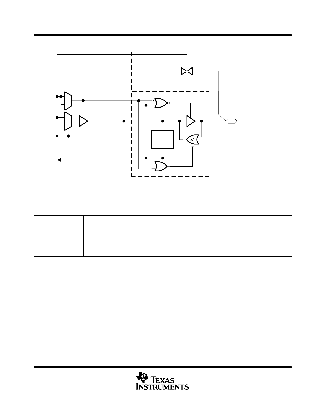
MSP430F42x0
MIXED SIGNAL MICROCONTROLLER
SLAS455D − MARCH 2005 − REVISED APRIL 2007
Port P6 pin schematic: P6.1, P6.3, input/output with Schmitt−trigger and analog functions
Ay−
P6DIR.x
P6OUT.x
DV
P6SEL.x
P6IN.x
#
#
SS
INCH=0/1
Note: x = 1,3
y = 0,1
#
Signal from or to SD16
Pad Logic
0
1
0
1
Direction
0: Input
1: Output
Bus
Keeper
EN
P6.1/A0−
P6.3/A1−
Port P6 (P6.1, P6.3) pin functions
PIN NAME (P6.X)
P6.1/A0− 1
P6.3/A1− 3
†
Default after reset (PUC/POR)
NOTES: 1. N/A: Not available or not applicable.
2. X: Don’t care.
3. Setting the P6SEL.x bit disables the output driver as well as the input Schmitt trigger to prevent parasitic cross currents when
applying analog signals.
X FUNCTION
P6.1† Input/Output 0/1 0
A0− (see Note 3) X 1
P6.3† Input/Output 0/1 0
A1− (see Note 3) X 1
CONTROL BITS / SIGNALS
P6DIR.x P6SEL.x
POST OFFICE BOX 655303 • DALLAS, TEXAS 75265
51

MSP430F42x0
MIXED SIGNAL MICROCONTROLLER
SLAS455D − MARCH 2005 − REVISED APRIL 2007
Port P6 pin schematic: P6.4 to P6.7, input/output with Schmitt−trigger and analog functions
P6DIR.x
P6OUT.x
DV
SS
P6SEL.x
P6IN.x
Note: x = 4 to 7
0
1
0
1
Direction
0: Input
1: Output
Bus
Keeper
EN
Pad Logic
P6.4
P6.5
P6.6
P6.7
Port P6 (P6.4 to P6.7) pin functions
PIN NAME (P6.X)
X FUNCTION
P6.4 4 P6.4† Input/Output 0/1 0
N/A 0 1
DVSS 1 1
P6.5 5 P6.5† Input/Output 0/1 0
N/A 0 1
DVSS 1 1
P6.6 6 P6.6† Input/Output 0/1 0
N/A 0 1
DVSS 1 1
P6.7 7 P6.7† Input/Output 0/1 0
N/A 0 1
DVSS 1 1
†
Default after reset (PUC/POR)
NOTES: 1. N/A: Not available or not applicable.
2. X: Don’t care.
CONTROL BITS / SIGNALS
P6DIR.x P6SEL.x
52
POST OFFICE BOX 655303 • DALLAS, TEXAS 75265
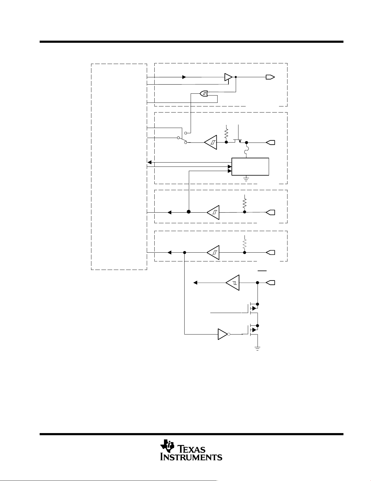
MSP430F42x0
MIXED SIGNAL MICROCONTROLLER
SLAS455D − MARCH 2005 − REVISED APRIL 2007
JTAG pins TMS, TCK, TDI/TCLK, TDO/TDI, input/output with Schmitt-trigger or output
TDO
Controlled by JTAG
Controlled by JTAG
Fuse
DV
TDO/TDI
TDI/TCLK
CC
TMS
JTAG
Test
and
Emulation
Module
Controlled
by JTAG
TDI
TMS
DV
CC
Burn and Test
TCK
TCK
Tau ~ 50 ns
Brownout
DV
CC
TCK
RST/NMI
D
G
G
U
S
D
U
S
POST OFFICE BOX 655303 • DALLAS, TEXAS 75265
53

MSP430F42x0
MIXED SIGNAL MICROCONTROLLER
SLAS455D − MARCH 2005 − REVISED APRIL 2007
JTAG fuse check mode
MSP430 devices that have the fuse on the TDI/TCLK terminal have a fuse check mode that tests the continuity
of the fuse the first time the JTAG port is accessed after a power-on reset (POR). When activated, a fuse check
current (I
taken to avoid accidentally activating the fuse check mode and increasing overall system power consumption.
Activation of the fuse check mode occurs with the first negative edge on the TMS pin after power up or if the
TMS is being held low during power up. The second positive edge on the TMS pin deactivates the fuse check
mode. After deactivation, the fuse check mode remains inactive until another POR occurs. After each POR the
fuse check mode has the potential to be activated.
The fuse check current only flows when the fuse check mode is active and the TMS pin is in a low state (see
Figure 19). Therefore, the additional current flow can be prevented by holding the TMS pin high (default
condition). The JTAG pins are terminated internally and therefore do not require external termination.
) of 1 mA at 3 V can flow from the TDI/TCLK pin to ground if the fuse is not burned. Care must be
(TF)
Time TMS Goes Low After POR
TMS
I
(TF)
I
TDI/TCLK
Figure 19. Fuse Check Mode Current
54
POST OFFICE BOX 655303 • DALLAS, TEXAS 75265

MIXED SIGNAL MICROCONTROLLER
Data Sheet Revision History
MSP430F42x0
SLAS455D − MARCH 2005 − REVISED APRIL 2007
Literature
Number
Updated functional block diagram (page 4)
Clarified test conditions in recommended operating conditions table (page 17)
Clarified test conditions in electrical characteristics table (page 18)
SLAS455D
NOTE: Page and figure numbers refer to the respective document revision.
Clarified test conditions in DCO table (page 25)
Changed PSRR to AC PSRR in SD16_A, performance table (page 29)
Changed PSRR to DC PSR in SD16_A, built-in voltage reference table; corrected typical value from 10 to 100 μV/V
(page 30)
Summary
POST OFFICE BOX 655303 • DALLAS, TEXAS 75265
55

PACKAGE OPTION ADDENDUM
www.ti.com
16-Jan-2007
PACKAGING INFORMATION
Orderable Device Status
(1)
Package
Type
Package
Drawing
Pins Package
Qty
Eco Plan
MSP430F4250IDL ACTIVE SSOP DL 48 25 Green (RoHS &
no Sb/Br)
MSP430F4250IDLR ACTIVE SSOP DL 48 1000 Green (RoHS &
no Sb/Br)
MSP430F4250IRGZR ACTIVE QFN RGZ 48 2500 Green (RoHS &
no Sb/Br)
MSP430F4250IRGZT ACTIVE QFN RGZ 48 250 Green (RoHS &
no Sb/Br)
MSP430F4260IDL ACTIVE SSOP DL 48 25 Green (RoHS &
no Sb/Br)
MSP430F4260IDLR ACTIVE SSOP DL 48 1000 Green (RoHS &
no Sb/Br)
MSP430F4260IRGZR ACTIVE QFN RGZ 48 2500 Green (RoHS &
no Sb/Br)
MSP430F4260IRGZT ACTIVE QFN RGZ 48 250 Green (RoHS &
no Sb/Br)
MSP430F4270IDL ACTIVE SSOP DL 48 25 Green (RoHS &
no Sb/Br)
MSP430F4270IDLR ACTIVE SSOP DL 48 1000 Green (RoHS &
no Sb/Br)
MSP430F4270IRGZR ACTIVE QFN RGZ 48 2500 Green (RoHS &
no Sb/Br)
MSP430F4270IRGZT ACTIVE QFN RGZ 48 250 Green (RoHS &
no Sb/Br)
(1)
The marketing status values are defined as follows:
ACTIVE: Product device recommended for new designs.
LIFEBUY: TI has announced that the device will be discontinued, and a lifetime-buy period is in effect.
NRND: Not recommended for new designs. Device is in production to support existing customers, but TI does not recommend using this part in
a new design.
PREVIEW: Device has been announced but is not in production. Samples may or may not be available.
OBSOLETE: TI has discontinued the production of the device.
(2)
Lead/Ball Finish MSL Peak Temp
CU NIPDAU Level-2-260C-1 YEAR
CU NIPDAU Level-2-260C-1 YEAR
CU NIPDAU Level-3-260C-168 HR
CU NIPDAU Level-3-260C-168 HR
CU NIPDAU Level-2-260C-1 YEAR
CU NIPDAU Level-2-260C-1 YEAR
CU NIPDAU Level-3-260C-168 HR
CU NIPDAU Level-3-260C-168 HR
CU NIPDAU Level-2-260C-1 YEAR
CU NIPDAU Level-2-260C-1 YEAR
CU NIPDAU Level-3-260C-168 HR
CU NIPDAU Level-3-260C-168 HR
(3)
(2)
Eco Plan - The planned eco-friendly classification: Pb-Free (RoHS), Pb-Free (RoHS Exempt), or Green (RoHS & no Sb/Br) - please check
http://www.ti.com/productcontent for the latest availability information and additional product content details.
TBD: The Pb-Free/Green conversion plan has not been defined.
Pb-Free (RoHS): TI's terms "Lead-Free" or "Pb-Free" mean semiconductor products that are compatible with the current RoHS requirements
for all 6 substances, including the requirement that lead not exceed 0.1% by weight in homogeneous materials. Where designed to be soldered
at high temperatures, TI Pb-Free products are suitable for use in specified lead-free processes.
Pb-Free (RoHS Exempt): This component has a RoHS exemption for either 1) lead-based flip-chip solder bumps used between the die and
package, or 2) lead-based die adhesive used between the die and leadframe. The component is otherwise considered Pb-Free (RoHS
compatible) as defined above.
Green (RoHS & no Sb/Br): TI defines "Green" to mean Pb-Free (RoHS compatible), and free of Bromine (Br) and Antimony (Sb) based flame
retardants (Br or Sb do not exceed 0.1% by weight in homogeneous material)
(3)
MSL, Peak Temp. -- The Moisture Sensitivity Level rating according to the JEDEC industry standard classifications, and peak solder
temperature.
Important Information and Disclaimer:The information provided on this page represents TI's knowledge and belief as of the date that it is
provided. TI bases its knowledge and belief on information provided by third parties, and makes no representation or warranty as to the
accuracy of such information. Efforts are underway to better integrate information from third parties. TI has taken and continues to take
reasonable steps to provide representative and accurate information but may not have conducted destructive testing or chemical analysis on
incoming materials and chemicals. TI and TI suppliers consider certain information to be proprietary, and thus CAS numbers and other limited
information may not be available for release.
Addendum-Page 1

PACKAGE OPTION ADDENDUM
www.ti.com
In no event shall TI's liability arising out of such information exceed the total purchase price of the TI part(s) at issue in this document sold by TI
to Customer on an annual basis.
16-Jan-2007
Addendum-Page 2


IMPORTANT NOTICE
Texas Instruments Incorporated and its subsidiaries (TI) reserve the right to make corrections, modifications, enhancements, improvements,
and other changes to its products and services at any time and to discontinue any product or service without notice. Customers should
obtain the latest relevant information before placing orders and should verify that such information is current and complete. All products are
sold subject to TI’s terms and conditions of sale supplied at the time of order acknowledgment.
TI warrants performance of its hardware products to the specifications applicable at the time of sale in accordance with TI’s standard
warranty. Testing and other quality control techniques are used to the extent TI deems necessary to support this warranty. Except where
mandated by government requirements, testing of all parameters of each product is not necessarily performed.
TI assumes no liability for applications assistance or customer product design. Customers are responsible for their products and
applications using TI components. To minimize the risks associated with customer products and applications, customers should provide
adequate design and operating safeguards.
TI does not warrant or represent that any license, either express or implied, is granted under any TI patent right, copyright, mask work right,
or other TI intellectual property right relating to any combination, machine, or process in which TI products or services are used. Information
published by TI regarding third-party products or services does not constitute a license from TI to use such products or services or a
warranty or endorsement thereof. Use of such information may require a license from a third party under the patents or other intellectual
property of the third party, or a license from TI under the patents or other intellectual property of TI.
Reproduction of TI information in TI data books or data sheets is permissible only if reproduction is without alteration and is accompanied
by all associated warranties, conditions, limitations, and notices. Reproduction of this information with alteration is an unfair and deceptive
business practice. TI is not responsible or liable for such altered documentation. Information of third parties may be subject to additional
restrictions.
Resale of TI products or services with statements different from or beyond the parameters stated by TI for that product or service voids all
express and any implied warranties for the associated TI product or service and is an unfair and deceptive business practice. TI is not
responsible or liable for any such statements.
TI products are not authorized for use in safety-critical applications (such as life support) where a failure of the TI product would reasonably
be expected to cause severe personal injury or death, unless officers of the parties have executed an agreement specifically governing
such use. Buyers represent that they have all necessary expertise in the safety and regulatory ramifications of their applications, and
acknowledge and agree that they are solely responsible for all legal, regulatory and safety-related requirements concerning their products
and any use of TI products in such safety-critical applications, notwithstanding any applications-related information or support that may be
provided by TI. Further, Buyers must fully indemnify TI and its representatives against any damages arising out of the use of TI products in
such safety-critical applications.
TI products are neither designed nor intended for use in military/aerospace applications or environments unless the TI products are
specifically designated by TI as military-grade or "enhanced plastic." Only products designated by TI as military-grade meet military
specifications. Buyers acknowledge and agree that any such use of TI products which TI has not designated as military-grade is solely at
the Buyer's risk, and that they are solely responsible for compliance with all legal and regulatory requirements in connection with such use.
TI products are neither designed nor intended for use in automotive applications or environments unless the specific TI products are
designated by TI as compliant with ISO/TS 16949 requirements. Buyers acknowledge and agree that, if they use any non-designated
products in automotive applications, TI will not be responsible for any failure to meet such requirements.
Following are URLs where you can obtain information on other Texas Instruments products and application solutions:
Products Applications
Amplifiers amplifier.ti.com Audio www.ti.com/audio
Data Converters dataconverter.ti.com Automotive www.ti.com/automotive
DSP dsp.ti.com Broadband www.ti.com/broadband
Clocks and Timers www.ti.com/clocks Digital Control www.ti.com/digitalcontrol
Interface interface.ti.com Medical www.ti.com/medical
Logic logic.ti.com Military www.ti.com/military
Power Mgmt power.ti.com Optical Networking www.ti.com/opticalnetwork
Microcontrollers microcontroller.ti.com Security www.ti.com/security
RFID www.ti-rfid.com Telephony www.ti.com/telephony
RF/IF and ZigBee® Solutions www.ti.com/lprf Video & Imaging www.ti.com/video
Mailing Address: Texas Instruments, Post Office Box 655303, Dallas, Texas 75265
Copyright © 2008, Texas Instruments Incorporated
Wireless www.ti.com/wireless
 Loading...