

Page 1
现货库存、技术资料、百科信息、热点资讯,精彩尽在鼎好!
www.ti.com
1
2
3
4
5
6
7
8
9
10
11
12
13
14
28
27
26
25
24
23
22
21
20
19
18
17
16
15
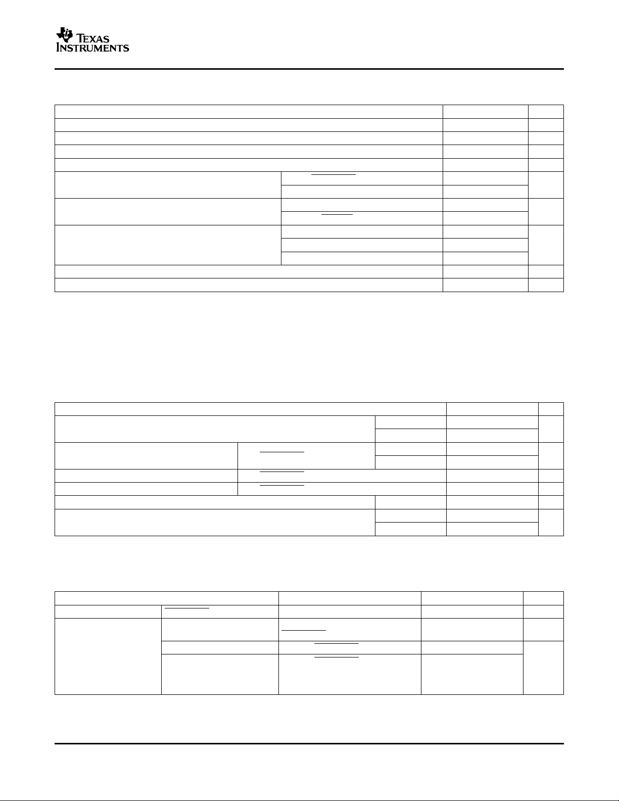
C2+
C2−
V−
RIN1
RIN2
RIN3
RIN4
RIN5
DOUT1
DOUT2
DOUT3
DIN3
DIN2
DIN1
C1+
V+
V
CC
GND
C1−
FORCEON
FORCEOFF
INVALID
ROUT2B
ROUT1
ROUT2
ROUT3
ROUT4
ROUT5
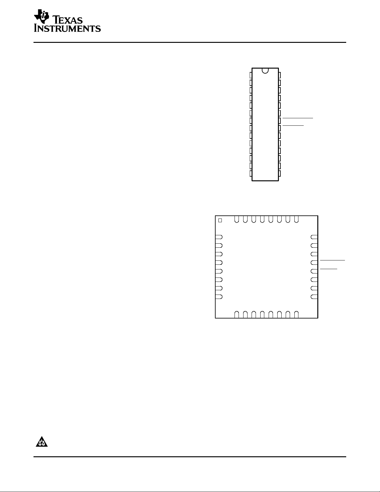
DB, DW, OR PW PACKAGE
(TOP VIEW)
QFN PACKAGE
(TOP VIEW)
GND
C1–
FORCEON
FORCEOFF
INVALID
ROUTB2
ROUT1
ROUT2
RIN1
RIN2
RIN3
RIN4
RIN5
DOUT1
DOUT2
DOUT3
NCV–C2–
C2+
C1+V+VCCNC
NC
DIN3
DIN2
DIN1
ROUT5
ROUT4
ROUT3
NC
1
2
3
4
5
6
7
8
24
23
22
21
20
19
18
17
3132 30 29 28 27 26 25
109 11 12 13 14 15 16
3-V TO 5.5-V MULTICHANNEL RS-232 LINE DRIVER/RECEIVER
FEATURES
• Single-Chip and Single-Supply Interface for
IBM™ PC/AT™ Serial Port
• ESD Protection for RS-232 Bus Pins
– ± 15-kV Human-Body Model (HBM)
– ± 8-kV IEC61000-4-2, Contact Discharge
– ± 15-kV IEC61000-4-2, Air-Gap Discharge
• Meets or Exceeds Requirements of
TIA/EIA-232-F and ITU v.28 Standards
• Operates With 3-V to 5.5-V V
• Always-Active Noninverting Receiver Output
(ROUT2B)
• Designed to Transmit at a Data Rate up to
500 kbit/s
• Low Standby Current . . . 1 µ A Typ
• External Capacitors . . . 4 × 0.1 µ F
• Accepts 5-V Logic Input With 3.3-V Supply
• Designed to Be Interchangeable With Maxim
MAX3243E
• Serial-Mouse Driveability
• Auto-Powerdown Feature to Disable Driver
Outputs When No Valid RS-232 Signal Is
Sensed
• Applications
– Battery-Powered Systems, PDAs,
Notebooks, Laptops, Palmtop PCs, and
Hand-Held Equipment
• Package Options Include Plastic
Small-Outline (DW), Shrink Small-Outline
(DB), and Thin Shrink Small-Outline (PW)
Packages
Supply
CC
MAX3243E
WITH ± 15-kV IEC ESD PROTECTION
SLLS657A – APRIL 2005 – REVISED JUNE 2005
DESCRIPTION
The MAX3243E device consists of three line drivers, five line receivers, and a dual charge-pump circuit with
± 15-kV ESD (HBM and IEC61000-4-2, Air-Gap Discharge) and ± 8-kV ESD (IEC61000-4-2, Contact Discharge)
protection on serial-port connection pins. The device meets the requirements of TIA/EIA-232-F and provides the
electrical interface between an asynchronous communication controller and the serial-port connector. This
combination of drivers and receivers matches that needed for the typical serial port used in an IBM PC/AT, or
compatible. The charge pump and four small external capacitors allow operation from a single 3-V to 5.5-V
supply. In addition, the device includes an always-active noninverting output (ROUT2B), which allows
applications using the ring indicator to transmit data while the device is powered down. The device operates at
data signaling rates up to 250 kbit/s and a maximum of 30-V/ µ s driver output slew rate.
PRODUCTION DATA information is current as of publication date.
Products conform to specifications per the terms of the Texas
Instruments standard warranty. Production processing does not
necessarily include testing of all parameters.
IBM, PC/AT are trademarks of International Business Machines Corporation.
Copyright © 2005, Texas Instruments Incorporated
Please be aware that an important notice concerning availability, standard warranty, and use in critical applications of Texas
Instruments semiconductor products and disclaimers thereto appears at the end of this data sheet.
Page 2
www.ti.com
MAX3243E
3-V TO 5.5-V MULTICHANNEL RS-232 LINE DRIVER/RECEIVER
WITH ± 15-kV IEC ESD PROTECTION
SLLS657A – APRIL 2005 – REVISED JUNE 2005
DESCRIPTION (CONTINUED)
Flexible control options for power management are available when the serial port is inactive. The
auto-powerdown feature functions when FORCEON is low and FORCEOFF is high. During this mode of
operation, if the device does not sense a valid RS-232 signal, the driver outputs are disabled. If FORCEOFF is
set low, both drivers and receivers (except ROUT2B) are shut off, and the supply current is reduced to 1 µ A.
Disconnecting the serial port or turning off the peripheral drivers causes the auto-powerdown condition to occur.
Auto-powerdown can be disabled when FORCEON and FORCEOFF are high, and should be done when driving
a serial mouse. With auto-powerdown enabled, the device is activated automatically when a valid signal is
applied to any receiver input. The INVALID output is used to notify the user if an RS-232 signal is present at any
receiver input. INVALID is high (valid data) if any receiver input voltage is greater than 2.7 V or less than –2.7 V
or has been between –0.3 V and 0.3 V for less than 30 µ s. INVALID is low (invalid data) if all receiver input
voltages are between –0.3 V and 0.3 V for more than 30 µ s. Refer to Figure 5 for receiver input levels.
The MAX3243EC is characterized for operation from 0 ° C to 70 ° C. The MAX3243EI is characterized for operation
from –40 ° C to 85 ° C.
AVAILABLE OPTIONS
(1)
MAX3243ECRHBR
(Preview)
(Preview)
T
A
0 ° C to 70 ° C MAX3243ECDB MAX3243ECDW MAX3243ECPW
–40 ° C to 85 ° C MAX3243EIDW MAX3243EIPW
MAX3243EIDB MAX3243EIRHBR
SHRINK THIN SHRINK QUAD FLAT
SMALL OUTLINE SMALL OUTLINE NO-LEAD
(DB) (PW) (RHB)
SMALL OUTLINE
(DB)
PACKAGED DEVICES
(1) The DB, DW, and PW packages are available in both tube and taped & reeled. Add the suffix R to orderable (e.g. MAX3243ECDBR for
taped & reeled version).
2
Page 3
www.ti.com
3-V TO 5.5-V MULTICHANNEL RS-232 LINE DRIVER/RECEIVER
WITH ± 15-kV IEC ESD PROTECTION
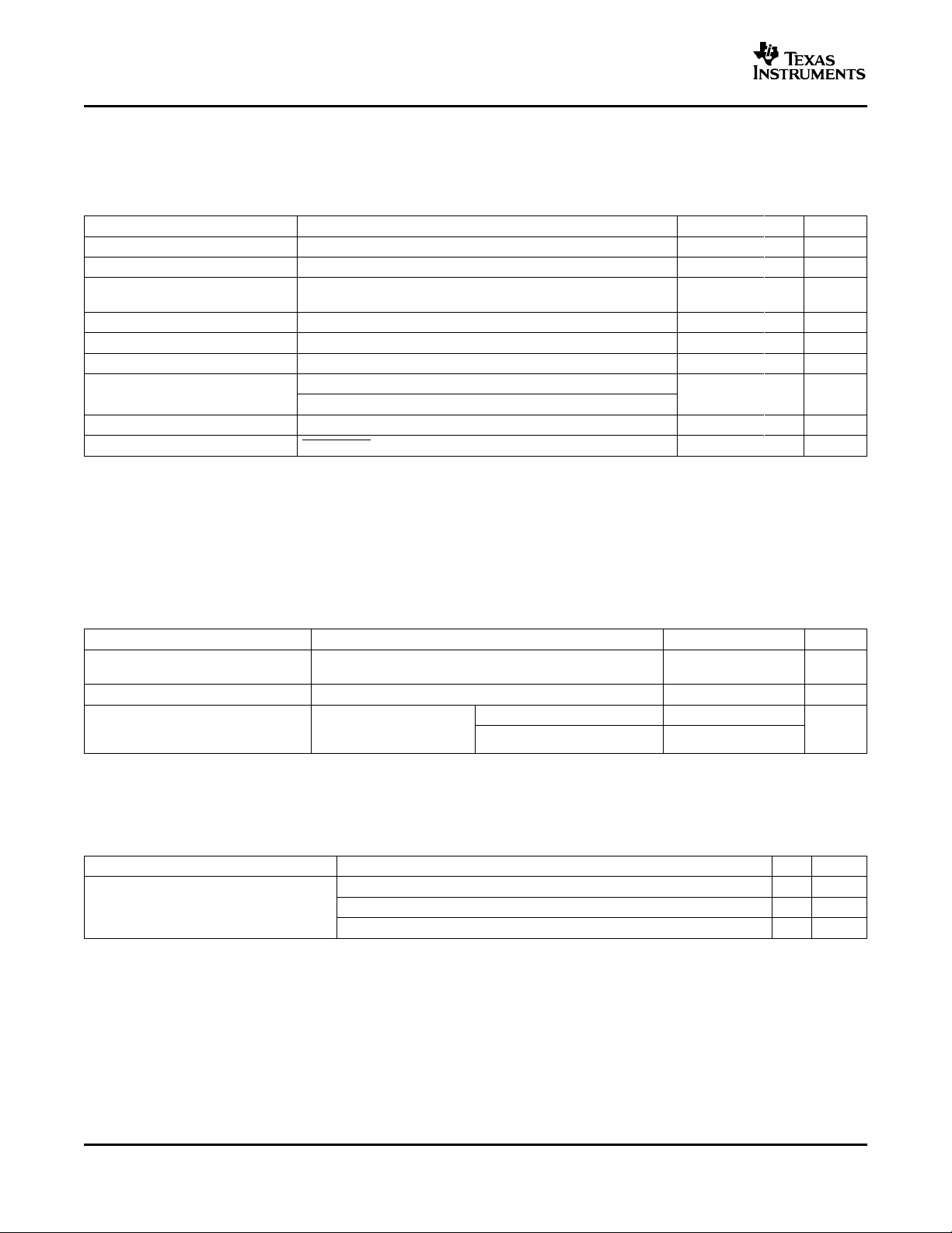
FUNCTION TABLES
ABC
EACH DRIVER
INPUTS
DIN FORCEON FORCEOFF
X X L X Z Powered off
L H H X H
H H H X L
L L H Yes H
H L H Yes L
L L H No Z
H L H No Z
(1) H = high level, L = low level, X = irrelevant, Z = high impedance
VALID RIN
RS-232 LEVEL
(1)
OUTPUT
DOUT
auto-powerdown disabled
auto-powerdown enabled
MAX3243E
SLLS657A – APRIL 2005 – REVISED JUNE 2005
DRIVER STATUS
Normal operation with
Normal operation with
Powered off by
auto-powerdown feature
EACH RECEIVER
INPUTS OUTPUTS
RIN2 FORCEOFF ROUT2B ROUT
L X L X L Z
H X L X H Z
L L H Yes L H
L H H Yes L L
H L H Yes H H
H H H Yes H L
Open Open H Yes L H
(1) H = high level, L = low level, X = irrelevant, Z = high impedance (off), Open = input disconnected or
RIN1, VALID RIN
RIN3-RIN5 RS-232 LEVEL
connected driver off
(1)
RECEIVER
STATUS
Powered off while
ROUT2B is active
Normal operation
with
auto-powerdown
disabled/enabled
3
Page 4
www.ti.com
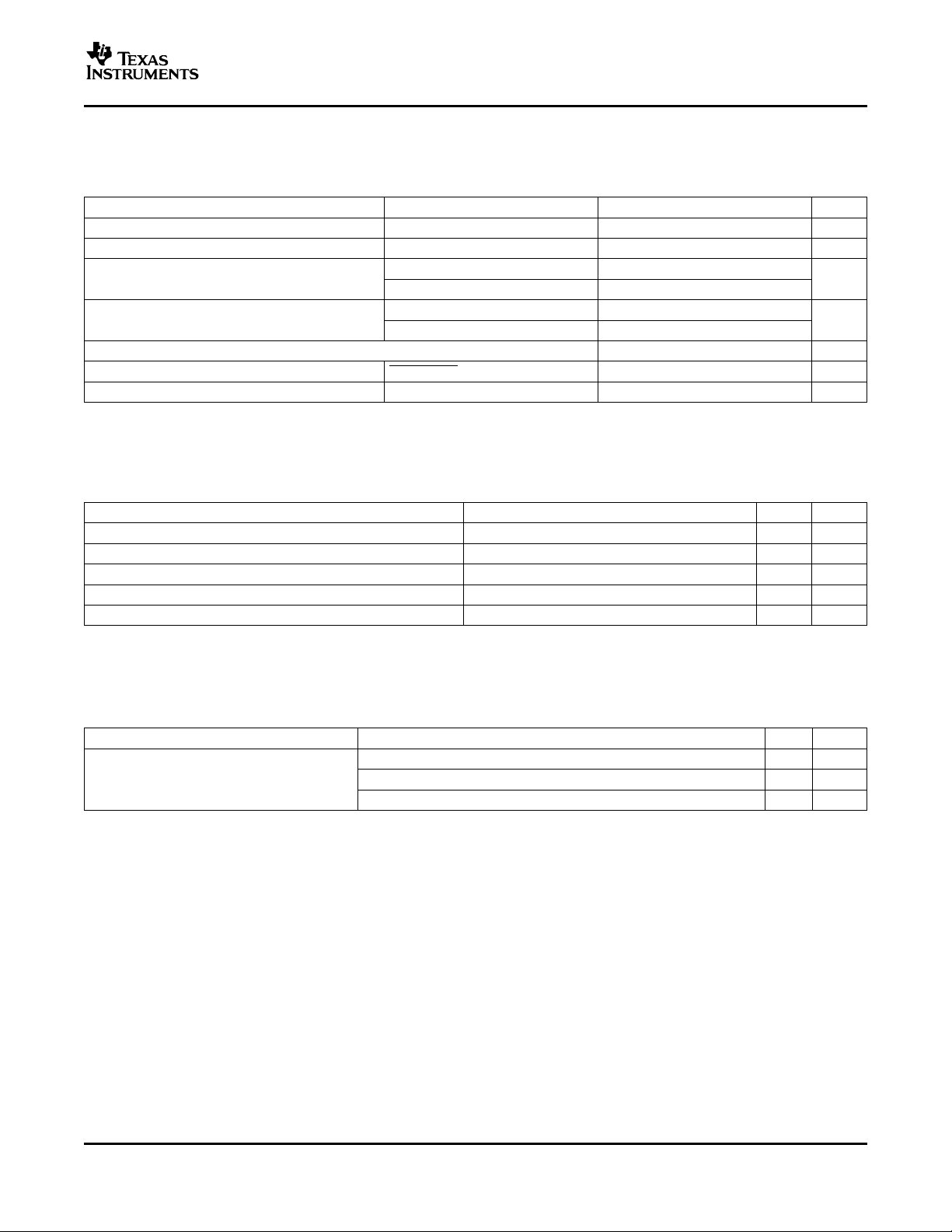
DIN3
DIN2
DIN1
DOUT3
DOUT2
DOUT1
Auto-powerdown INVALID
RIN1
RIN2
RIN3
RIN4
RIN5
FORCEOFF
FORCEON
ROUT1
ROUT2B
ROUT2
ROUT3
ROUT4
ROUT5
14
13
12
22
23
19
20
18
17
16
15
9
10
11
21
4
5
6
7
8
MAX3243E
3-V TO 5.5-V MULTICHANNEL RS-232 LINE DRIVER/RECEIVER
WITH ± 15-kV IEC ESD PROTECTION
SLLS657A – APRIL 2005 – REVISED JUNE 2005
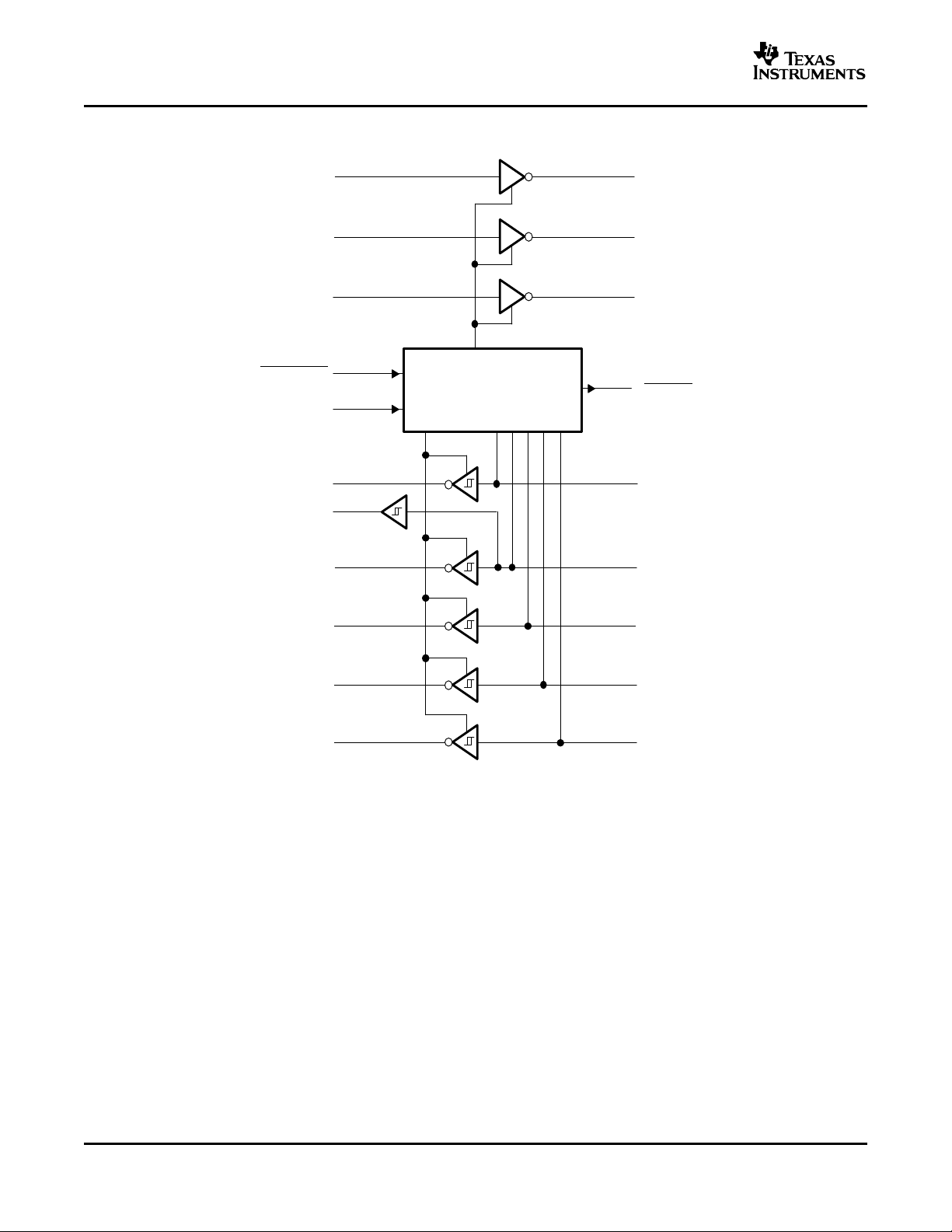
LOGIC DIAGRAM (POSITIVE LOGIC)
4
Page 5
www.ti.com
3-V TO 5.5-V MULTICHANNEL RS-232 LINE DRIVER/RECEIVER
WITH ± 15-kV IEC ESD PROTECTION
SLLS657A – APRIL 2005 – REVISED JUNE 2005
Absolute Maximum Ratings
over operating free-air temperature range (unless otherwise noted)
V
CC
V+ Positive output supply voltage range
V– Negative output supply voltage range
V+ – V– Output supply voltage difference
V
I
V
O
θ
JA
T
stg
(1) Stresses beyond those listed under "absolute maximum ratings" may cause permanent damage to the device. These are stress ratings
(2) All voltages are with respect to network GND.
(3) Maximum power dissipation is a function of TJ(max), θJA, and TA. The maximum allowable power dissipation at any allowable ambient
(4) The package thermal impedance is calculated in accordance with JESD 51-7.
Supply voltage range
Input voltage range V
Output voltage range V
Package thermal impedance
Lead temperature 1,6 mm (1/16 in) from case for 10 s 260 °C
Storage temperature range –65 150 °C
only, and functional operation of the device at these or any other conditions beyond those indicated under "recommended operating
conditions" is not implied. Exposure to absolute-maximum-rated conditions for extended periods may affect device reliability.
temperature is PD= (TJ(max) - TA)/ θJA. Operating at the absolute maximum TJof 150 ° C can affect reliability.
(1)
MIN MAX UNIT
(2)
(2)
(2)
(2)
–0.3 6 V
–0.3 7 V
0.3 –7 V
Driver ( FORCEOFF, FORCEON) –0.3 6
Receiver –25 25
Driver –13.2 13.2
Receiver ( INVALID) –0.3 V
CC
DB package 62
(3) (4)
DW package 46 °C/W
PW package 62
MAX3243E
13 V
+ 0.3
Recommended Operating Conditions
(1)
See Figure 6
MIN NOM MAX UNIT
V
= 3.3 V 3 3.3 3.6
Supply voltage V
V
Driver and control high-level input voltage DIN, FORCEOFF, FORCEON V
IH
V
Driver and control low-level input voltage DIN, FORCEOFF, FORCEON 0.8 V
IL
V
Driver and control input voltage DIN, FORCEOFF, FORCEON 0 5.5 V
I
V
Receiver input voltage –25 25 V
I
T
Operating free-air temperature °C
A
(1) Test conditions are C1–C4 = 0.1 µ F at V
Electrical Characteristics
(1)
= 3.3 V ± 0.3 V; C1 = 0.047 µ F, C2–C4 = 0.33 µ F at V
CC
CC
V
= 5 V 4.5 5 5.5
CC
V
= 3.3 V 2
CC
V
= 5 V 2.4
CC
MAX3243EC 0 70
MAX3243EI –40 85
= 5 V ± 0.5 V.
CC
over recommended ranges of supply voltage and operating free-air temperature (unless otherwise noted) (see Figure 6 )
PARAMETER TEST CONDITIONS MIN TYP
I
Input leakage current FORCEOFF, FORCEON ±0.01 ±1 µ A
I
Auto-powerdown disabled 0.3 1 mA
Supply current
I
CC
(T
= 25 ° C)
A
Powered off No load, FORCEOFF at GND 1 10
Auto-powerdown enabled 1 10
No load,
FORCEOFF and FORCEON at V
No load, FORCEOFF at VCC,
FORCEON at GND,
All RIN are open or grounded,
CC
All DIN are grounded
(2)
MAX UNIT
µ A
(1) Test conditions are C1–C4 = 0.1 µ F at V
(2) All typical values are at V
= 3.3 V or V
CC
= 3.3 V ± 0.3 V; C1 = 0.047 µ F, C2–C4 = 0.33 µ F at V
CC
= 5 V, and TA= 25 ° C.
CC
= 5 V ± 0.5 V.
CC
5
Page 6
www.ti.com
MAX3243E
3-V TO 5.5-V MULTICHANNEL RS-232 LINE DRIVER/RECEIVER
WITH ± 15-kV IEC ESD PROTECTION
SLLS657A – APRIL 2005 – REVISED JUNE 2005
DRIVER SECTION
Electrical Characteristics
(1)
over recommended ranges of supply voltage and operating free-air temperature (unless otherwise noted) (see Figure 6 )
PARAMETER TEST CONDITIONS MIN TYP
V
High-level output voltage All DOUT at RL= 3 k Ω to GND 5 5.4 V
OH
V
Low-level output voltage All DOUT at RL= 3 k Ω to GND –5 –5.4 V
OL
Output voltage DIN1 = DIN2 = GND, DIN3 = VCC, 3-k Ω to GND at DOUT3,
V
O
(mouse driveability) DOUT1 = DOUT2 = 2.5 mA
I
High-level input current VI= V
IH
I
Low-level input current VIat GND ± 0.01 ± 1 µ A
IL
V
Input hysteresis ± 1 V
hys
I
Short-circuit output current
OS
r
Output resistance VCC, V+, and V– = 0 V, VO= ± 2 V 300 10M Ω
o
I
Output leakage current FORCEOFF = GND, VO= ± 12 V, V
off
(3)
(1) Test conditions are C1–C4 = 0.1 µ F at V
(2) All typical values are at V
(3) Short-circuit durations should be controlled to prevent exceeding the device absolute power dissipation ratings, and not more than one
= 3.3 V or V
CC
CC
V
= 3.6 V, VO= 0 V
CC
V
= 5.5 V, VO= 0 V
CC
= 3.3 V ± 0.3 V; C1 = 0.047 µ F, C2–C4 = 0.33 µ F at V
CC
= 5 V, and TA= 25 ° C.
CC
= 0 to 5.5 V ± 25 µ A
CC
± 5 V
= 5 V ± 0.5 V.
CC
output should be shorted at a time.
Switching Characteristics
(1)
(2)
MAX UNIT
± 0.01 ± 1 µ A
± 60 mA
switching characteristics over recommended ranges of supply voltage and operating free-air temperature (unless otherwise
noted) (see Figure 6 )
PARAMETER TEST CONDITIONS MIN TYP
Maximum data rate 250 500 kbit/s
t
SR(tr) RL= 3 k Ω to 7 k Ω , V/ µ s
sk(p)
Pulse skew
Slew rate, transition region
(see Figure 1)
(3)
(1) Test conditions are C1–C4 = 0.1 µ F at V
(2) All typical values are at V
(3) Pulse skew is defined as |t
CC
PLH
CL= 1000 pF, RL= 3 k Ω
One DOUT switching, See Figure 1
CL= 150 pF to 2500 pF, RL= 3 k Ω to 7 k Ω , See Figure 2 100 ns
V
= 3.3 V, CL= 150 pF to 1000 pF 6 30
CC
PRR = 250 kbit/s
= 3.3 V or V
– t
CC
CC
| of each channel of the same device.
PHL
= 3.3 V + 0.3 V; C1 = 0.047 µ F, C2–C4 = 0.33 µ F at V
= 5 V, and TA= 25 ° C.
CL= 150 pF to 2500 pF 4 30
= 5 V ± 0.5 V.
CC
(2)
MAX UNIT
ESD Protection
PARAMETER TEST CONDITIONS TYP UNIT
HBM ± 15 kV
Driver outputs (pins 9–11) IEC61000-4-2, Air-Gap Discharge ± 15 kV
IEC61000-4-2, Contact Discharge ± 8 kV
6
Page 7
www.ti.com
RECEIVER SECTION
MAX3243E
3-V TO 5.5-V MULTICHANNEL RS-232 LINE DRIVER/RECEIVER
WITH ± 15-kV IEC ESD PROTECTION
SLLS657A – APRIL 2005 – REVISED JUNE 2005
Electrical Characteristics
(1)
over recommended ranges of supply voltage and operating free-air temperature (unless otherwise noted) (see Figure 6 )
PARAMETER TEST CONDITIONS MIN TYP
V
OH
V
OL
V
IT+
V
IT–
V
hys
I
off
r
i
High-level output voltage IOH= –1 mA V
Low-level output voltage IOH= 1.6 mA 0.4 V
Positive-going input threshold voltage V
Negative-going input threshold voltage V
Input hysteresis (V
– V
IT+
) 0.5 V
IT–
Output leakage current (except ROUT2B) FORCEOFF = 0 V ± 0.05 ± 10 µ A
Input resistance VI= ± 3 V or ± 25 V 3 5 7 k Ω
(1) Test conditions are C1–C4 = 0.1 µ F at V
(2) All typical values are at V
Switching Characteristics
= 3.3 V or V
CC
(1)
V
= 3.3 V 1.6 2.4
CC
V
= 5 V 1.9 2.4
CC
V
= 3.3 V 0.6 1.1
CC
V
= 5 V 0.8 1.4
CC
= 3.3 V ± 0.3 V; C1 = 0.047 µ F, C2–C4 = 0.33 µ F at V
CC
= 5 V, and TA= 25 ° C.
CC
CC
– 0.6 V
= 5 V ± 0.5 V.
CC
(2)
MAX UNIT
– 0.1 V
CC
over recommended ranges of supply voltage and operating free-air temperature (unless otherwise noted)
PARAMETER TEST CONDITIONS TYP
t
PLH
t
PHL
t
en
t
dis
t
sk(p)
Propagation delay time, low- to high-level output CL= 150 pF, See Figure 3 150 ns
Propagation delay time, high- to low-level output 150 ns
Output enable time CL= 150 pF, RL= 3 k Ω , See Figure 4 200 ns
Output disable time 200 ns
Puse skew
(3)
(1) Test conditions are C1–C4 = 0.1 µ F at V
(2) All typical values are at V
(3) Pulse skew is defined as |t
= 3.3 V or V
CC
PLH
- t
PHL
See Figure 3 50 ns
= 3.3 V ± 0.3 V; C1 = 0.047 µ F, C2–C4 = 0.33 µ F at V
CC
= 5 V, and TA= 25 ° C.
CC
| of each channel of the same device.
= 5 V ± 0.5 V.
CC
(2)
UNIT
ESD Protection
PARAMETER TEST CONDITIONS TYP UNIT
HBM ± 15 kV
Driver outputs (pins 4–8) IEC61000-4-2, Air-Gap discharge ± 15 kV
IEC61000-4-2, Contact Discharge ± 8 kV
7
Page 8
www.ti.com
MAX3243E
3-V TO 5.5-V MULTICHANNEL RS-232 LINE DRIVER/RECEIVER
WITH ± 15-kV IEC ESD PROTECTION
SLLS657A – APRIL 2005 – REVISED JUNE 2005
AUTO-POWERDOWN SECTION
Electrical Characteristics
over recommended ranges of supply voltage and operating free-air temperature (unless otherwise noted) (see Figure 5 )
PARAMETER TEST CONDITIONS MIN MAX UNIT
V
IT+(valid)
V
IT–(valid)
V
T(invalid)
V
OH
V
OL
Switching Characteristics
over recommended ranges of supply voltage and operating free-air temperature (unless otherwise noted) (see Figure 5 )
t
valid
t
invalid
t
en
Receiver input threshold FORCEON = GND,
for INVALID high-level output voltage FORCEOFF = V
Receiver input threshold FORCEON = GND,
for INVALID high-level output voltage FORCEOFF = V
Receiver input threshold FORCEON = GND,
for INVALID low-level output voltage FORCEOFF = V
INVALID high-level output voltage V
INVALID low-level output voltage 0.4 V
IOH= -1 mA, FORCEON = GND,
FORCEOFF = V
IOL= 1.6 mA, FORCEON = GND,
FORCEOFF = V
CC
CC
CC
CC
CC
–2.7 V
–0.3 0.3 V
– 0.6 V
CC
PARAMETER TEST CONDITIONS TYP
Propagation delay time, low- to high-level output V
Propagation delay time, high- to low-level output V
Supply enable time V
= 5 V 1 µ s
CC
= 5 V 30 µ s
CC
= 5 V 100 µ s
CC
2.7 V
(1)
UNIT
(1) All typical values are at V
= 3.3 V or V
CC
= 5 V, and TA= 25 ° C.
CC
8
Page 9

www.ti.com
50 Ω
TEST CIRCUIT VOLTAGE WAVEFORMS
−3 V
−3 V
3 V
3 V
0 V
3 V
Output
Input
V
OL
V
OH
t
TLH
Generator
(see Note B)
R
L
3 V
FORCEOFF
RS-232
Output
t
THL
C
L
(see Note A)
SR(tr)
6 V
t
THL
or t
TLH
NOTES: A. CL includes probe and jig capacitance.
B. The pulse generator has the following characteristics: ZO = 50 Ω, 50% duty cycle, tr ≤ 10 ns, tf ≤ 10 ns.
50 Ω
TEST CIRCUIT VOLTAGE WAVEFORMS
0 V
3 V
Output
Input
V
OL
V
OH
t
PLH
Generator
(see Note B)
R
L
3 V
FORCEOFF
RS-232
Output
t
PHL
C
L
(see Note A)
NOTES: A. CL includes probe and jig capacitance.
B. The pulse generator has the following characteristics: PRR = 250 kbit/s, ZO = 50 Ω, 50% duty cycle, tr ≤ 10 ns, tf ≤ 10 ns.
50%
50%
1.5 V
1.5 V
TEST CIRCUIT VOLTAGE WAVEFORMS
50 Ω
−3 V
3 V
Output
Input
V
OL
V
OH
t
PHL
Generator
(see Note B)
t
PLH
Output
C
L
(see Note A)
3 V or 0 V
FORCEON
NOTES: A. CL includes probe and jig capacitance.
B. The pulse generator has the following characteristics: ZO = 50 Ω, 50% duty cycle, tr ≤ 10 ns, tf ≤ 10 ns.
3 V
FORCEOFF
1.5 V 1.5 V
50% 50%
3-V TO 5.5-V MULTICHANNEL RS-232 LINE DRIVER/RECEIVER
PARAMETER MEASUREMENT INFORMATION
Figure 1. Driver Slew Rate
MAX3243E
WITH ± 15-kV IEC ESD PROTECTION
SLLS657A – APRIL 2005 – REVISED JUNE 2005
Figure 2. Driver Pulse Skew
Figure 3. Receiver Propagation Delay Times
9
Page 10

www.ti.com
TEST CIRCUIT VOLTAGE WAVEFORMS
50 Ω
Generator
(see Note B)
3 V or 0 V
Output
V
OL
V
OH
t
PZH
(S1 at GND)
3 V
−3 V
0.3 V
Output
Input
0.3 V
3 V or 0 V
FORCEON
FORCEOFF
NOTES: A. CL includes probe and jig capacitance.
B. The pulse generator has the following characteristics: ZO = 50 Ω, 50% duty cycle, tr ≤ 10 ns, tf ≤ 10 ns.
C. t
PLZ
and t
PHZ
are the same as t
dis
.
D. t
PZL
and t
PZH
are the same as ten.
1.5 V 1.5 V
50%
t
PHZ
(S1 at GND)
t
PLZ
(S1 at VCC)
50%
t
PZL
(S1 at VCC)
R
L
S1
V
CC
GND
C
L
(see Note A)
Output
MAX3243E
3-V TO 5.5-V MULTICHANNEL RS-232 LINE DRIVER/RECEIVER
WITH ± 15-kV IEC ESD PROTECTION
SLLS657A – APRIL 2005 – REVISED JUNE 2005
PARAMETER MEASUREMENT INFORMATION
10
Figure 4. Receiver Enable and Disable Times
Page 11

www.ti.com
TEST CIRCUIT VOLTAGE WAVEFORMS
50 Ω
3 V
2.7 V
−2.7 V
INVALID
Output
Receiver
Input
Generator
(see Note B)
FORCEOFF
t
valid
ROUT
FORCEON
Auto-
powerdown
INVALID
DOUT
0 V
0 V
−3 V
DIN
C
L
= 30 pF
(see Note A)
V
CC
0 V
2.7 V
−2.7 V
0.3 V
−0.3 V
0 V
Valid RS-232 Level, INVALID High
Indeterminate
Indeterminate
If Signal Remains Within This Region
For More Than 30 µs, INVALID
Is Low
†
Valid RS-232 Level, INVALID
High
†
Auto-powerdown disables drivers and reduces supply
current to 1 µA.
≈V+
0 V
≈V−
V+
V
CC
t
en
V−
NOTES: A. CL includes probe and jig capacitance.
B. The pulse generator has the following characteristics: PRR = 5 kbit/s, ZO = 50 Ω, 50% duty cycle, tr ≤ 10 ns, tf ≤ 10 ns.
50% V
CC
50% V
CC
2.7 V
−2.7 V
0.3 V
0.3 V
t
invalid
Supply
Voltages
3-V TO 5.5-V MULTICHANNEL RS-232 LINE DRIVER/RECEIVER
PARAMETER MEASUREMENT INFORMATION
MAX3243E
WITH ± 15-kV IEC ESD PROTECTION
SLLS657A – APRIL 2005 – REVISED JUNE 2005
Figure 5. INVALID Propagation Delay Timnes and Supply Enabling Time
11
Page 12

www.ti.com
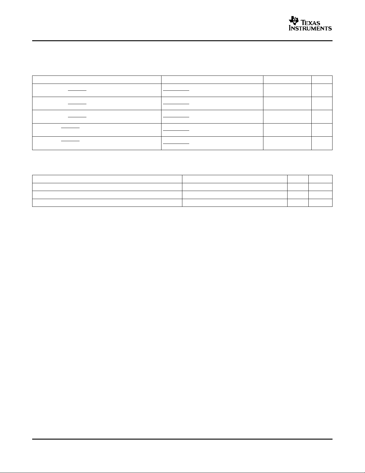
RIN4
DOUT2
DOUT3
ROUT1
FORCEOFF
RIN5
INVALID
ROUT2
DOUT1
ROUT2B
DIN3
DIN2
ROUT3
ROUT4
DIN1
ROUT5
C4
+
−
+
−
C3
†
V
CC
C2+
C2−
C1
C1+
GND
V−
C1−
FORCEON
C2
+
−
C
BYPASS
= 0.1 µF
V+
+
−
+
−
RIN1
RIN2
RIN3
RS-232 Inputs
Logic Outputs
Logic Inputs
RS-232 Outputs
V
CC
C1 C2, C3, and C4
3.3 V ± 0.3 V
5 V ± 0.5 V
3 V to 5.5 V
0.1 µF
0.047 µF
0.1 µF
0.1 µF
0.33 µF
0.47 µF
†
C3 can be connected to VCC or GND.
NOTES: A. Resistor values shown are nominal.
B. Nonpolarized ceramic capacitors are acceptable. If polarized tantalum or
electrolytic capacitors are used, they should be connected as shown.
V
CC
vs CAPACITOR VALUES
Auto-
powerdown
1
2
4
5
6
7
8
9
10
11
12
13
14
3
28
27
26
25
24
23
22
21
20
19
18
17
16
15
5 kΩ
5 kΩ
5 kΩ
5 kΩ
5 kΩ
MAX3243E
3-V TO 5.5-V MULTICHANNEL RS-232 LINE DRIVER/RECEIVER
WITH ± 15-kV IEC ESD PROTECTION
SLLS657A – APRIL 2005 – REVISED JUNE 2005
APPLICATION INFORMATION
12
Figure 6. Typical Operating Circuit and Capacitor Values
Page 13

www.ti.com
−
+
DUT
R
D
1.5 kΩ
V
HBM
100 pF
C
S
MAX3243E
3-V TO 5.5-V MULTICHANNEL RS-232 LINE DRIVER/RECEIVER
WITH ± 15-kV IEC ESD PROTECTION
SLLS657A – APRIL 2005 – REVISED JUNE 2005
APPLICATION INFORMATION
ESD Protection
TI MAX3243E devices have standard ESD protection structures incorporated on the pins to protect against
electrostatic discharges encountered during assembly and handling. In addition, the RS232 bus pins (driver
outputs and receiver inputs) of these devices have an extra level of ESD protection. Advanced ESD structures
were designed to successfully protect these bus pins against ESD discharge of ± 15-kV in all states: normal
operation, shutdown, and powered down. The MAX3243E devices are designed to continue functioning properly
after an ESD occurrence without any latchup.
The MAX3243E devices have three specified ESD limits on the driver outputs and receiver inputs, with respect to
GND:
• ± 15-kV Human Body Model (HBM)
• ± 15-kV IEC61000-4-2, Air-Gap Discharge (formerly IEC1000-4-2)
• ± 8-kV IEC61000-4-2, Contact Discharge
ESD Test Conditions
ESD testing is stringently performed by TI, based on various conditions and procedures. Please contact TI for a
reliability report that documents test setup, methodology, and results.
Human Body Model (HBM)
The Human Body Model of ESD testing is shown in Figure 7, while Figure 8 shows the current waveform that is
generated during a discharge into a low impedance. The model consists of a 100-pF capacitor, charged to the
ESD voltage of concern, and subsequently discharged into the DUT through a 1.5k- Ω resistor.
Figure 7. HBM ESD Test Circuit
13
Page 14

www.ti.com
100 150 20050
0
1.5
1.0
0.5
0.0
DUT = 10-V 1-Ω Zener Diode
V
HBM
= 2 kV
Time (ns)
I
DUT
(A)
−
+
DUT
150 pF
C
S
R
C
R
D
50−100 MΩ 330 Ω
High-Voltage
DC Source
MAX3243E
3-V TO 5.5-V MULTICHANNEL RS-232 LINE DRIVER/RECEIVER
WITH ± 15-kV IEC ESD PROTECTION
SLLS657A – APRIL 2005 – REVISED JUNE 2005
APPLICATION INFORMATION
Figure 8. Typical HBM Current Waveform
IEC61000-4-2 (Formerly Known as IEC1000-4-2)
Unlike the HBM, MM, and CDM ESD tests that apply to component level integrated circuits, the IEC61000-4-2 is
a system-level ESD testing and performance standard that pertains to the end equipment. The MAX3243E is
designed to enable the manufacturer in meeting the highest level (Level 4) of IEC61000-4-2 ESD protection with
no further need of external ESD protection circuitry. The more stringent IEC test standard has a higher peak
current than the HBM, due to the lower series resistance in the IEC model.
Figure 9 shows the IEC61000-4-2 model, and Figure 10 shows the current waveform for the corresponding
± 8-kV Contact-Discharge (Level 4) test. This waveform is applied to a probe that has been connected to the
DUT. On the other hand, the corresponding ± 15-kV (Level 4) Air-Gap Discharge test involves approaching the
DUT with an already energized probe.
Figure 9. Simplified IEC61000-4-2 ESD Test Circuit
14
Page 15

www.ti.com
(30A) 100%
90%
10%
30 ns
60 ns
I
t
tr = 0.7 ns to 1 ns
I
Peak
(8A)
(16A)
(V
contact
= 8 kV)
3-V TO 5.5-V MULTICHANNEL RS-232 LINE DRIVER/RECEIVER
APPLICATION INFORMATION
MAX3243E
WITH ± 15-kV IEC ESD PROTECTION
SLLS657A – APRIL 2005 – REVISED JUNE 2005
Figure 10. Typical Current Waveform of IEC61000-4-2 ESD Generator
Machine Model
The Machine Model (MM) ESD test applies to all pins using a 200-pF capacitor with no discharge resistance.
The purpose of the MM test is to simulate possible ESD conditions that can occur during the handling and
assembly processes of manufacturing. In this case, ESD protection is required for all pins, not just RS-232 pins.
However, after PC board assembly, the MM test is no longer as pertinent to the RS-232 pins.
15
Page 16

PACKAGE OPTION ADDENDUM
www.ti.com
12-Sep-2006
PACKAGING INFORMATION
Orderable Device Status
MAX3243ECDB ACTIVE SSOP DB 28 50 Green (RoHS &
MAX3243ECDBE4 ACTIVE SSOP DB 28 50 Green (RoHS &
MAX3243ECDBR ACTIVE SSOP DB 28 2000 Green (RoHS &
MAX3243ECDBRE4 ACTIVE SSOP DB 28 2000 Green (RoHS &
MAX3243ECDW ACTIVE SOIC DW 28 20 Green (RoHS &
MAX3243ECDWR ACTIVE SOIC DW 28 1000 Green (RoHS &
MAX3243ECPW ACTIVE TSSOP PW 28 50 Green (RoHS &
MAX3243ECPWE4 ACTIVE TSSOP PW 28 50 Green (RoHS &
MAX3243ECPWR ACTIVE TSSOP PW 28 2000 Green (RoHS &
MAX3243ECPWRE4 ACTIVE TSSOP PW 28 2000 Green (RoHS &
MAX3243ECRHBR ACTIVE QFN RHB 32 3000 Green (RoHS &
MAX3243ECRHBRG4 ACTIVE QFN RHB 32 3000 Green (RoHS &
MAX3243EIDB ACTIVE SSOP DB 28 50 Green (RoHS &
MAX3243EIDBR ACTIVE SSOP DB 28 2000 Green (RoHS &
MAX3243EIDW ACTIVE SOIC DW 28 20 Green (RoHS &
MAX3243EIDWR ACTIVE SOIC DW 28 1000 Green (RoHS &
MAX3243EIPW ACTIVE TSSOP PW 28 50 Green (RoHS &
MAX3243EIPWE4 ACTIVE TSSOP PW 28 50 Green (RoHS &
MAX3243EIPWR ACTIVE TSSOP PW 28 2000 Green (RoHS &
MAX3243EIPWRE4 ACTIVE TSSOP PW 28 2000 Green (RoHS &
MAX3243EIRHBR ACTIVE QFN RHB 32 3000 Green (RoHS &
MAX3243EIRHBRG4 ACTIVE QFN RHB 32 3000 Green (RoHS &
(1)
The marketing status valuesare defined as follows:
ACTIVE: Product device recommended for new designs.
LIFEBUY: TI has announced that the device will be discontinued, and a lifetime-buy period is in effect.
NRND: Not recommended for new designs. Device is in production to support existing customers, but TI does not recommend using this part in
a new design.
PREVIEW: Device has been announced but is not in production. Samples may or may not be available.
(1)
Package
Type
Package
Drawing
Pins Package
Qty
Eco Plan
no Sb/Br)
no Sb/Br)
no Sb/Br)
no Sb/Br)
no Sb/Br)
no Sb/Br)
no Sb/Br)
no Sb/Br)
no Sb/Br)
no Sb/Br)
no Sb/Br)
no Sb/Br)
no Sb/Br)
no Sb/Br)
no Sb/Br)
no Sb/Br)
no Sb/Br)
no Sb/Br)
no Sb/Br)
no Sb/Br)
no Sb/Br)
no Sb/Br)
(2)
Lead/Ball Finish MSL Peak Temp
CU NIPDAU Level-1-260C-UNLIM
CU NIPDAU Level-1-260C-UNLIM
CU NIPDAU Level-1-260C-UNLIM
CU NIPDAU Level-1-260C-UNLIM
CU NIPDAU Level-1-260C-UNLIM
CU NIPDAU Level-1-260C-UNLIM
CU NIPDAU Level-1-260C-UNLIM
CU NIPDAU Level-1-260C-UNLIM
CU NIPDAU Level-1-260C-UNLIM
CU NIPDAU Level-1-260C-UNLIM
CU NIPDAU Level-2-260C-1YEAR
CU NIPDAU Level-2-260C-1YEAR
CU NIPDAU Level-1-260C-UNLIM
CU NIPDAU Level-1-260C-UNLIM
CU NIPDAU Level-1-260C-UNLIM
CU NIPDAU Level-1-260C-UNLIM
CU NIPDAU Level-1-260C-UNLIM
CU NIPDAU Level-1-260C-UNLIM
CU NIPDAU Level-1-260C-UNLIM
CU NIPDAU Level-1-260C-UNLIM
CU NIPDAU Level-2-260C-1YEAR
CU NIPDAU Level-2-260C-1YEAR
(3)
Addendum-Page 1
Page 17

PACKAGE OPTION ADDENDUM
www.ti.com
OBSOLETE: TI has discontinued the production of the device.
(2)
Eco Plan - The planned eco-friendly classification: Pb-Free (RoHS), Pb-Free (RoHS Exempt), or Green (RoHS & no Sb/Br) - please check
http://www.ti.com/productcontent for the latest availability information and additional product content details.
TBD: The Pb-Free/Green conversion plan has not been defined.
Pb-Free (RoHS): TI's terms "Lead-Free" or "Pb-Free" mean semiconductor products that are compatible with the current RoHS requirements
for all 6 substances, including the requirement that lead not exceed 0.1% by weight in homogeneous materials. Where designed to be soldered
at high temperatures, TI Pb-Free products are suitable for use in specified lead-free processes.
Pb-Free (RoHS Exempt): This component has a RoHS exemption for either 1) lead-based flip-chip solder bumps used between the die and
package, or 2) lead-based die adhesive used between the die and leadframe. The component is otherwise considered Pb-Free (RoHS
compatible) as defined above.
Green (RoHS & no Sb/Br): TI defines "Green" to mean Pb-Free (RoHS compatible), and free of Bromine (Br) and Antimony (Sb) based flame
retardants (Br or Sb do not exceed 0.1% by weight in homogeneous material)
(3)
MSL, Peak Temp. -- The Moisture Sensitivity Level rating according to the JEDEC industry standard classifications, and peak solder
temperature.
Important Information and Disclaimer:The information provided on this page represents TI's knowledge and belief as of the date that it is
provided. TI bases its knowledge and belief on information provided by third parties, and makes no representation or warranty as to the
accuracy of such information. Efforts are underway to better integrate information from third parties. TI has taken and continues to take
reasonable steps to provide representative and accurate information but may not have conducted destructive testing or chemical analysis on
incoming materials and chemicals. TI and TI suppliers consider certain information to be proprietary, and thus CAS numbers and other limited
information may not be available for release.
In no event shall TI's liability arising out of such information exceed the total purchase price of the TI part(s) at issue in this document sold by TI
to Customer on an annual basis.
12-Sep-2006
Addendum-Page 2
Page 18

Page 19

Page 20

Page 21

Page 22

MECHANICAL DATA
MSSO002E – JANUARY 1995 – REVISED DECEMBER 2001
DB (R-PDSO-G**) PLASTIC SMALL-OUTLINE
28 PINS SHOWN
0,65
28
1
2,00 MAX
0,38
0,22
15
14
A
0,05 MIN
0,15
5,60
5,00
M
8,20
7,40
Seating Plane
0,10
0,25
0,09
0°–ā8°
Gage Plane
0,25
0,95
0,55
PINS **
DIM
A MAX
A MIN
NOTES: A. All linear dimensions are in millimeters.
B. This drawing is subject to change without notice.
C. Body dimensions do not include mold flash or protrusion not to exceed 0,15.
D. Falls within JEDEC MO-150
14
6,50
6,50
5,905,90
2016
7,50
6,90
24
8,50
28
10,50
9,907,90
30
10,50
9,90
38
12,90
12,30
4040065 /E 12/01
POST OFFICE BOX 655303 • DALLAS, TEXAS 75265
Page 23

MECHANICAL DATA
MTSS001C – JANUARY 1995 – REVISED FEBRUARY 1999
PW (R-PDSO-G**) PLASTIC SMALL-OUTLINE PACKAGE
14 PINS SHOWN
0,65
1,20 MAX
14
0,30
0,19
8
4,50
4,30
PINS **
7
Seating Plane
0,15
0,05
8
1
A
DIM
6,60
6,20
14
0,10
0,10
M
0,15 NOM
Gage Plane
0,25
0°–8°
2016
24
28
0,75
0,50
A MAX
A MIN
NOTES: A. All linear dimensions are in millimeters.
B. This drawing is subject to change without notice.
C. Body dimensions do not include mold flash or protrusion not to exceed 0,15.
D. Falls within JEDEC MO-153
3,10
2,90
5,10
4,90
5,10
4,90
6,60
6,40
7,90
7,70
9,80
9,60
4040064/F 01/97
POST OFFICE BOX 655303 • DALLAS, TEXAS 75265
Page 24

IMPORTANT NOTICE
Texas Instruments Incorporated and its subsidiaries (TI) reserve the right to make corrections, modifications,
enhancements, improvements, and other changes to its products and services at any time and to
discontinue any product or service without notice. Customers should obtain the latest relevant information
before placing orders and should verify that such information is current and complete. All products are sold
subject to TI’s terms and conditions of sale supplied at the time of order acknowledgment.
TI warrants performance of its hardware products to the specifications applicable at the time of sale in
accordance with TI’s standard warranty. Testing and other quality control techniques are used to the extent
TI deems necessary to support this warranty. Except where mandated by government requirements, testing
of all parameters of each product is not necessarily performed.
TI assumes no liability for applications assistance or customer product design. Customers are responsible
for their products and applications using TI components. To minimize the risks associated with customer
products and applications, customers should provide adequate design and operating safeguards.
TI does not warrant or represent that any license, either express or implied, is granted under any TI patent
right, copyright, mask work right, or other TI intellectual property right relating to any combination, machine,
or process in which TI products or services are used. Information published by TI regarding third-party
products or services does not constitute a license from TI to use such products or services or a warranty or
endorsement thereof. Use of such information may require a license from a third party under the patents or
other intellectual property of the third party, or a license from TI under the patents or other intellectual
property of TI.
Reproduction of information in TI data books or data sheets is permissible only if reproduction is without
alteration and is accompanied by all associated warranties, conditions, limitations, and notices.
Reproduction of this information with alteration is an unfair and deceptive business practice. TI is not
responsible or liable for such altered documentation.
Resale of TI products or services with statements different from or beyond the parameters stated by TI for
that product or service voids all express and any implied warranties for the associated TI product or service
and is an unfair and deceptive business practice. TI is not responsible or liable for any such statements.
Following are URLs where you can obtain information on other Texas Instruments products and application
solutions:
Products
Applications
Amplifiers amplifier.ti.com Audio www.ti.com/audio
Data Converters dataconverter.ti.com Automotive www.ti.com/automotive
DSP dsp.ti.com Broadband www.ti.com/broadband
Interface interface.ti.com Digital Control www.ti.com/digitalcontrol
Logic logic.ti.com Military www.ti.com/military
Power Mgmt power.ti.com Optical Networking www.ti.com/opticalnetwork
Microcontrollers microcontroller.ti.com Security www.ti.com/security
Low Power Wireless www.ti.com/lpw Telephony www.ti.com/telephony
Video & Imaging www.ti.com/video
Wireless www.ti.com/wireless
Mailing Address: Texas Instruments
Post Office Box 655303 Dallas, Texas 75265
Copyright © 2007, Texas Instruments Incorporated
 Loading...