

Page 1
现货库存、技术资料、百科信息、热点资讯,精彩尽在鼎好!
www.ti.com
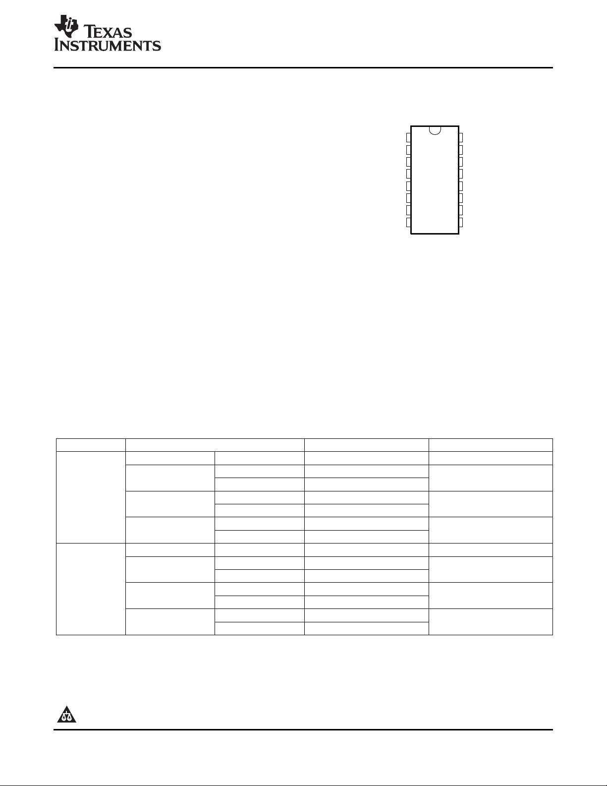
D,DW,N,ORPWPACKAGE
(TOP VIEW)
1
2
3
4
5
6
7
8
16
15
14
13
12
11
10
9
C1+
V+
C1-
C2+
C2-
V-
DOUT2
RIN2
V
CC
GND
DOUT1
RIN1
ROUT1
DIN1
DIN2
ROUT2
FEATURES
• ESD Protection for RS-232 Bus Pins
– ± 15-kV – Human-Body Model
• Meets or Exceeds the Requirements of
TIA/EIA-232-F and ITU v.28 Standards
• Operates at 5-V V
Supply
CC
• Operates Up to 120 kbit/s
• External Capacitors . . . 4 × 0.1 µ F
• Latch-Up Performance Exceeds 100 mA Per
JESD 78, Class II
APPLICATIONS
• Battery-Powered Systems
• PDAs
• Notebooks
• Laptops
• Palmtop PCs
• Hand-Held Equipment
MAX202
5-V DUAL RS-232 LINE DRIVER/RECEIVER
WITH ± 15-kV ESD PROTECTION
SLLS576E – JULY 2003 – REVISED APRIL 2007
DESCRIPTION/ORDERING INFORMATION
The MAX202 device consists of two line drivers, two line receivers, and a dual charge-pump circuit with ± 15-kV
ESD protection pin to pin (serial-port connection pins, including GND). The device meets the requirements of
TIA/EIA-232-F and provides the electrical interface between an asynchronous communication controller and the
serial-port connector. The charge pump and four small external capacitors allow operation from a single 5-V
supply. The device operates at data signaling rates up to 120 kbit/s and a maximum of 30-V/ µ s driver output
slew rate.
0 ° C to 70 ° C Tube of 40 MAX202CDW
–40 ° C to 85 ° C Tube of 40 MAX202IDW
(1) Package drawings, standard packing quantities, thermal data, symbolization, and PCB design guidelines are available at
www.ti.com/sc/package.
(2) For the most current package and ordering information, see the Package Option Addendum at the end of this document, or see the TI
website at www.ti.com .
PRODUCTION DATA information is current as of publication date.
Products conform to specifications per the terms of the Texas
Instruments standard warranty. Production processing does not
necessarily include testing of all parameters.
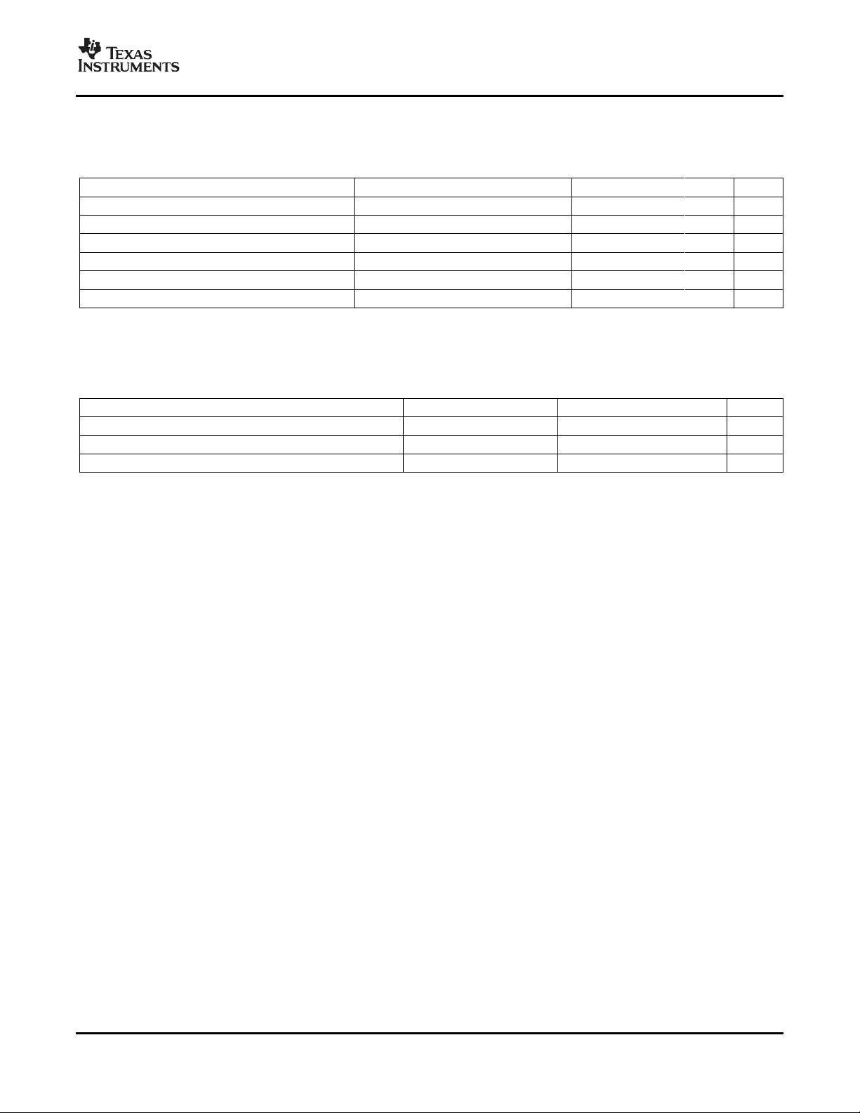
ORDERING INFORMATION
T
A
PDIP – N Tube of 25 MAX202CN MAX202CN
SOIC – D MAX202C
SOIC – DW MAX202C
TSSOP – PW MA202C
PDIP – N Tube of 25 MAX202IN MAX202IN
SOIC – D MAX202I
SOIC – DW MAX202I
TSSOP – PW MB202I
PACKAGE
Please be aware that an important notice concerning availability, standard warranty, and use in critical applications of Texas
Instruments semiconductor products and disclaimers thereto appears at the end of this data sheet.
(1) (2)
Tube of 40 MAX202CD
Reel of 2500 MAX202CDR
Reel of 2000 MAX202CDWR
Tube of 90 MAX202CPW
Reel of 2000 MAX202CPWR
Tube of 40 MAX202ID
Reel of 2500 MAX202IDR
Reel of 2000 MAX202IDWR
Tube of 90 MAX202IPW
Reel of 2000 MAX202IPWR
ORDERABLE PART NUMBER TOP-SIDE MARKING
Copyright © 2003–2007, Texas Instruments Incorporated
Page 2
www.ti.com
DIN1
DOUT1
RIN1ROUT1
DIN2
DOUT2
RIN2ROUT2
11
10
12
9
14
7
13
8
MAX202
5-V DUAL RS-232 LINE DRIVER/RECEIVER
WITH ± 15-kV ESD PROTECTION
SLLS576E – JULY 2003 – REVISED APRIL 2007
Function Tables
xxx
EACH DRIVER
INPUT OUTPUT
D
IN
L H
H L
(1) H = high level, L = low level
(1)
D
OUT
EACH RECEIVER
INPUT OUTPUT
R
IN
L H
H L
Open H
(1) H = high level, L = low level,
Open = input disconnected or
connected driver off
LOGIC DIAGRAM (POSITIVE LOGIC)
(1)
R
OUT
2
Submit Documentation Feedback
Page 3
www.ti.com
5-V DUAL RS-232 LINE DRIVER/RECEIVER
WITH ± 15-kV ESD PROTECTION
SLLS576E – JULY 2003 – REVISED APRIL 2007
Absolute Maximum Ratings
over operating free-air temperature range (unless otherwise noted)
V
CC
V+ Positive charge pump voltage range
V– Negative charge pump voltage range
V
I
V
O
D
OUT
θ
JA
T
J
T
stg
(1) Stresses beyond those listed under "absolute maximum ratings" may cause permanent damage to the device. These are stress ratings
(2) All voltages are with respect to network GND.
(3) Maximum power dissipation is a function of TJ(max), θJA, and TA. The maximum allowable power dissipation at any allowable ambient
(4) The package thermal impedance is calculated in accordance with JESD 51-7.
Supply voltage range
Input voltage range V
Output voltage range V
Short-circuit duration Continuous
Package thermal impedance
Operating virtual junction temperature 150 ° C
Storage temperature range –65 150 ° C
only, and functional operation of the device at these or any other conditions beyond those indicated under "recommended operating
conditions" is not implied. Exposure to absolute-maximum-rated conditions for extended periods may affect device reliability.
temperature is PD= (TJ(max) – TA)/ θJA. Operating at the absolute maximum TJof 150 ° C can affect reliability.
(1)
MIN MAX UNIT
(2)
(2)
(2)
–0.3 6 V
V
– 0.3 14 V
CC
–14 0.3 V
Drivers –0.3 V+ + 0.3
Receivers ± 30
Drivers V – –0.3 V+ + 0.3
Receivers –0.3 V
+ 0.3
CC
D package 73
(3) (4)
DW package 57
N package 67
PW package 108
MAX202
° C/W
Recommended Operating Conditions
(1)
(see Figure 4 )
MIN NOM MAX UNIT
Supply voltage 4.5 5 5.5 V
V
V
V
T
(1) Test conditions are C1–C4 = 0.1 µ F at V
Electrical Characteristics
Driver high-level input voltage D
IH
Driver low-level input voltage D
IL
Driver input voltage D
I
Receiver input voltage –30 30
Operating free-air temperature ° C
A
= 5 V ± 0.5 V.
CC
(1)
IN
IN
IN
MAX202C 0 70
MAX202I –40 85
2 V
0 5.5
0.8 V
over recommended ranges of supply voltage and operating free-air temperature (unless otherwise noted) (see Figure 4 )
PARAMETER TEST CONDITIONS MIN TYP
I
CC
Suppy current No load, V
(1) Test conditions are C1–C4 = 0.1 µ F at V
(2) All typical values are at V
= 5 V, and TA= 25 ° C.
CC
= 5 V ± 0.5 V.
CC
= 5 V 8 15 mA
CC
(2)
MAX UNIT
V
Submit Documentation Feedback
3
Page 4
www.ti.com
MAX202
5-V DUAL RS-232 LINE DRIVER/RECEIVER
WITH ± 15-kV ESD PROTECTION
SLLS576E – JULY 2003 – REVISED APRIL 2007
DRIVER SECTION
Electrical Characteristics
(1)
over recommended ranges of supply voltage and operating free-air temperature (unless otherwise noted) (see Figure 4 )
PARAMETER TEST CONDITIONS MIN TYP
V
V
I
IH
I
IL
I
OS
r
O
(1) Test conditions are C1–C4 = 0.1 µ F at V
(2) All typical values are at V
(3) Short-circuit durations should be controlled to prevent exceeding the device absolute power-dissipation ratings, and not more than one
High-level output voltage D
OH
Low-level output voltage D
OL
High-level input current VI= V
at RL= 3 k Ω to GND, DIN= GND 5 9 V
OUT
at RL= 3 k Ω to GND, DIN= V
OUT
CC
CC
–5 –9 V
Low-level input current VIat 0 V –15 –200 µ A
(3)
Short-circuit output current V
= 5.5 V VO= 0 V ± 10 ± 60 mA
CC
Output resistance VCC, V+, and V– = 0 V VO= ± 2 V 300 Ω
= 5 V ± 0.5 V.
= 5 V, and TA= 25 ° C.
CC
CC
output should be shorted at a time.
Switching Characteristics
(1)
(2)
MAX UNIT
15 200 µ A
over recommended ranges of suply voltage and operating free-air temperature (unless otherwise noted) (see Figure 4 )
PARAMETER TEST CONDITIONS MIN TYP
Maximum data rate 120 kbit/s
t
PLH(D)
t
PHL(D)
t
sk(p)
SR(tr) 3 6 30 V/ µ s
Propagation delay time, low- to
high-level output
Propagation delay time, high- to
low-level output
Pulse skew
(3)
Slew rate, transition region
(see Figure 1 )
(1) Test conditions are C1–C4 = 0.1 µ F at V
(2) All typical values are at V
(3) Pulse skew is defined as |t
= 5 V, and TA= 25 ° C.
CC
- t
PLH
| of each channel of the same device.
PHL
CL= 50 to 1000 pF, RL= 3 k Ω to 7 k Ω ,
One D
switching, See Figure 1
OUT
CL= 2500 pF, RL= 3 k Ω ,
All drivers loaded, See Figure 1
CL= 2500 pF, RL= 3 k Ω ,
All drivers loaded, See Figure 1
CL= 150 to 2500 pF, RL= 3 k Ω to 7 k Ω ,
See Figure 2
CL= 50 to 1000 pF, RL= 3 k Ω to 7 k Ω ,
V
= 5 V
CC
= 5 V ± 0.5 V.
CC
(2)
MAX UNIT
2 µ s
2 µ s
300 ns
ESD Protection
PIN TEST CONDITIONS TYP UNIT
D
, R
OUT
IN
4
Human-body model ± 15 kV
Submit Documentation Feedback
Page 5
www.ti.com
RECEIVER SECTION
MAX202
5-V DUAL RS-232 LINE DRIVER/RECEIVER
WITH ± 15-kV ESD PROTECTION
SLLS576E – JULY 2003 – REVISED APRIL 2007
Electrical Characteristics
(1)
over recommended ranges of supply voltage and operating free-air temperature (unless otherwise noted) (seeFigure 4 )
PARAMETER TEST CONDITIONS MIN TYP
V
V
V
V
V
r
i
High-level output voltage IOH= –1 mA 3.5 V
OH
Low-level output voltage IOL= 1.6 mA 0.4 V
OL
Positive-going input threshold voltage V
IT+
Negative-going input threshold voltage V
IT–
hys
Input hysteresis (V
– V
IT+
) 0.2 0.5 1 V
IT–
Input resistance VI= ± 3 V to ± 25 V 3 5 7 k Ω
(1) Test conditions are C1–C4 = 0.1 µ F at V
(2) All typical values are at V
Switching Characteristics
= 5 V, and TA= 25 ° C.
CC
(1)
= 5 V ± 0.5 V.
CC
= 5 V, TA= 25 ° C 1.7 2.4 V
CC
= 5 V, TA= 25 ° C 0.8 1.2 V
CC
(2)
MAX UNIT
– 0.4 V
CC
over recommended ranges of suply voltage and operating free-air temperature (unless otherwise noted) (see Figure 3 )
PARAMETER TEST CONDITIONS MIN TYP
t
PLH(R)
t
PHL(R)
t
sk(p)
Propagation delay time, low- to high-level output CL= 150 pF 0.5 10 µ s
Propagation delay time, high- to low-level output CL= 150 pF 0.5 10 µ s
Pulse skew
(3)
(1) Test conditions are C1–C4 = 0.1 µ F at V
(2) All typical values are at V
(3) Pulse skew is defined as |t
= 5 V, and TA= 25 ° C.
CC
- t
PLH
PHL
= 5 V ± 0.5 V.
CC
| of each channel of the same device.
(2)
MAX UNIT
300 ns
Submit Documentation Feedback
5
Page 6

www.ti.com
50 W
TESTCIRCUIT VOLTAGEWAVEFORMS
0V
3V
Output
Input
V
OL
V
OH
t
PLH(D)
Generator
(seeNoteB)
R
L
RS-232
Output
t
PHL (D)
C
L
(seeNote A)
NOTES: A.C includesprobeandjigcapacitance.
L
B. Thepulsegeneratorhasthefollowingcharacteristics:PRR=120kbit/s,Z =50 ,50%dutycycle,t 10ns,t 10ns.
O r f
W £ £
1.5V 1.5V
3V
–3V
3V
–3V
SR(tf)=
6V
t ort
PHL(D PLH(D)
)
TESTCIRCUIT VOLTAGEWAVEFORMS
0V
3V
Output
Input
V
OL
V
OH
t
PLH(D)
t
PHL (D)
50%
50%
NOTES: A.C includesprobeandjigcapacitance.
L
B. Thepulsegeneratorhasthefollowingcharacteristics:PRR=120kbit/s,Z =50 ,50%dutycycle,t 10ns,t 10ns.
O r f
W £ £
1.5V 1.5V
50 W
Generator
(seeNoteB)
R
L
RS-232
Output
C
L
(seeNote A)
TESTCIRCUIT VOLTAGEWAVEFORMS
50 W
50%
50%
–3V
3V
1.5V
1.5V
Output
Input
V
OL
V
OH
t
PHL (R)
Generator
(seeNoteB)
t
PLH(R)
Output
C
L
(seeNote A)
NOTES: A.C includesprobeandjigcapacitance.
L
B. Thepulsegeneratorhasthefollowingcharacteristics:Z =50 ,50%dutycycle,t 10ns,t 10ns.
O r f
W £ £
MAX202
5-V DUAL RS-232 LINE DRIVER/RECEIVER
WITH ± 15-kV ESD PROTECTION
SLLS576E – JULY 2003 – REVISED APRIL 2007
PARAMETER MEASUREMENT INFORMATION
Figure 1. Driver Slew Rate
6
Figure 2. Driver Pulse Skew
Figure 3. Receiver Propagation Delay Times
Submit Documentation Feedback
Page 7

www.ti.com
11
10
8
1
2
3
4
7
ROUT2
DIN2
9
RIN1
16
13
12
15
14
DIN1
5
6
+
–
V
CC
C2+
C1+
GND
C1–
ROUT1
C2–
+
–
CBYPASS
=0.1 F,m
V+
+
–
+
–
RIN2
+
–
DOUT1
DOUT2
†
C3canbeconnectedtoV orGND.
CC
NOTES: A .Resistorvaluesshownarenominal.
V–
C1
0.1 F,m
6.3V
C3
†
0.1 Fm
16V
C2
0.1 F,m
16V
5kW
5kW
C4
0.1 Fm ,
16V
B.Nonpolarizedceramiccapacitorsareacceptable.Ifpolarizedtantalumorelectrolyticcapacitorsareused,theyshouldbe
connectedasshown.
MAX202
5-V DUAL RS-232 LINE DRIVER/RECEIVER
WITH ± 15-kV ESD PROTECTION
SLLS576E – JULY 2003 – REVISED APRIL 2007
APPLICATION INFORMATION
Figure 4. Typical Operating Circuit and Capacitor Values
Capacitor Selection
The capacitor type used for C1–C4 is not critical for proper operation. The MAX202 requires 0.1- µ F capacitors,
although capacitors up to 10 µ F can be used without harm. Ceramic dielectrics are suggested for the 0.1- µ F
capacitors. When using the minimum recommended capacitor values, make sure the capacitance value does
not degrade excessively as the operating temperature varies. If in doubt, use capacitors with a larger (e.g., 2 × )
nominal value. The capacitors' effective series resistance (ESR), which usually rises at low temperatures,
influences the amount of ripple on V+ and V–.
Use larger capacitors (up to 10 µ F) to reduce the output impedance at V+ and V–.
Bypass V
charge pumps, decouple V
capacitors (C1–C4).
ESD Protection
to ground with at least 0.1 µ F. In applications sensitive to power-supply noise generated by the
CC
to ground with a capacitor the same size as (or larger than) the charge-pump
CC
TI MAX202 devices have standard ESD protection structures incorporated on the pins to protect against
electrostatic discharges encountered during assembly and handling. In addition, the RS232 bus pins (driver
outputs and receiver inputs) of these devices have an extra level of ESD protection. Advanced ESD structures
were designed to successfully protect these bus pins against ESD discharge of ± 15-kV when powered down.
Submit Documentation Feedback
7
Page 8

www.ti.com
-
+
DUT
R
D
1.5kW
V
HBM
100pF
C
S
100 150 20050
0
1.5
1.0
0.5
0.0
V =2kV
HBM
DUT=10-V,1-WZenerDiode
|
Time-ns
I - A
DUT
MAX202
5-V DUAL RS-232 LINE DRIVER/RECEIVER
WITH ± 15-kV ESD PROTECTION
SLLS576E – JULY 2003 – REVISED APRIL 2007
APPLICATION INFORMATION (continued)
ESD Test Conditions
Stringent ESD testing is performed by TI, based on various conditions and procedures. Please contact TI for a
reliability report that documents test setup, methodology, and results.
Human-Body Model (HBM)
The HBM of ESD testing is shown in Figure 5 . Figure 6 shows the current waveform that is generated during a
discharge into a low impedance. The model consists of a 100-pF capacitor, charged to the ESD voltage of
concern, and subsequently discharged into the device under test (DUT) through a 1.5-k Ω resistor.
Figure 5. HBM ESD Test Circuit
Figure 6. Typical HBM Current Waveform
Machine Model (MM)
The MM ESD test applies to all pins using a 200-pF capacitor with no discharge resistance. The purpose of the
MM test is to simulate possible ESD conditions that can occur during the handling and assembly processes of
manufacturing. In this case, ESD protection is required for all pins, not just RS-232 pins. However, after PC
board assembly, the MM test no longer is as pertinent to the RS-232 pins.
8
Submit Documentation Feedback
Page 9
PACKAGE OPTION ADDENDUM
www.ti.com
PACKAGING INFORMATION
Orderable Device Status
MAX202CD ACTIVE SOIC D 16 40 Green (RoHS &
MAX202CDE4 ACTIVE SOIC D 16 40 Green (RoHS &
MAX202CDR ACTIVE SOIC D 16 2500 Green (RoHS &
MAX202CDRE4 ACTIVE SOIC D 16 2500 Green (RoHS &
MAX202CDW ACTIVE SOIC DW 16 40 Green (RoHS &
MAX202CDWE4 ACTIVE SOIC DW 16 40 Green (RoHS &
MAX202CDWR ACTIVE SOIC DW 16 2000 Green (RoHS &
MAX202CDWRE4 ACTIVE SOIC DW 16 2000 Green (RoHS &
MAX202CPW ACTIVE TSSOP PW 16 90 Green (RoHS &
MAX202CPWE4 ACTIVE TSSOP PW 16 90 Green (RoHS &
MAX202CPWR ACTIVE TSSOP PW 16 2000 Green (RoHS &
MAX202CPWRE4 ACTIVE TSSOP PW 16 2000 Green (RoHS &
MAX202ID ACTIVE SOIC D 16 40 Green (RoHS &
MAX202IDE4 ACTIVE SOIC D 16 40 Green (RoHS &
MAX202IDR ACTIVE SOIC D 16 2500 Green (RoHS &
MAX202IDRE4 ACTIVE SOIC D 16 2500 Green (RoHS &
MAX202IDW ACTIVE SOIC DW 16 40 Green (RoHS &
MAX202IDWE4 ACTIVE SOIC DW 16 40 Green (RoHS &
MAX202IDWR ACTIVE SOIC DW 16 2000 Green (RoHS &
MAX202IDWRE4 ACTIVE SOIC DW 16 2000 Green (RoHS &
MAX202IPW ACTIVE TSSOP PW 16 90 Green (RoHS &
MAX202IPWE4 ACTIVE TSSOP PW 16 90 Green (RoHS &
MAX202IPWR ACTIVE TSSOP PW 16 2000 Green (RoHS &
MAX202IPWRE4 ACTIVE TSSOP PW 16 2000 Green (RoHS &
(1)
The marketing status values are defined as follows:
(1)
Package
Type
Package
Drawing
Pins Package
Qty
Eco Plan
no Sb/Br)
no Sb/Br)
no Sb/Br)
no Sb/Br)
no Sb/Br)
no Sb/Br)
no Sb/Br)
no Sb/Br)
no Sb/Br)
no Sb/Br)
no Sb/Br)
no Sb/Br)
no Sb/Br)
no Sb/Br)
no Sb/Br)
no Sb/Br)
no Sb/Br)
no Sb/Br)
no Sb/Br)
no Sb/Br)
no Sb/Br)
no Sb/Br)
no Sb/Br)
no Sb/Br)
(2)
Lead/Ball Finish MSL Peak Temp
CU NIPDAU Level-1-260C-UNLIM
CU NIPDAU Level-1-260C-UNLIM
CU NIPDAU Level-1-260C-UNLIM
CU NIPDAU Level-1-260C-UNLIM
CU NIPDAU Level-1-260C-UNLIM
CU NIPDAU Level-1-260C-UNLIM
CU NIPDAU Level-1-260C-UNLIM
CU NIPDAU Level-1-260C-UNLIM
CU NIPDAU Level-1-260C-UNLIM
CU NIPDAU Level-1-260C-UNLIM
CU NIPDAU Level-1-260C-UNLIM
CU NIPDAU Level-1-260C-UNLIM
CU NIPDAU Level-1-260C-UNLIM
CU NIPDAU Level-1-260C-UNLIM
CU NIPDAU Level-1-260C-UNLIM
CU NIPDAU Level-1-260C-UNLIM
CU NIPDAU Level-1-260C-UNLIM
CU NIPDAU Level-1-260C-UNLIM
CU NIPDAU Level-1-260C-UNLIM
CU NIPDAU Level-1-260C-UNLIM
CU NIPDAU Level-1-260C-UNLIM
CU NIPDAU Level-1-260C-UNLIM
CU NIPDAU Level-1-260C-UNLIM
CU NIPDAU Level-1-260C-UNLIM
29-Mar-2007
(3)
Addendum-Page 1
Page 10

PACKAGE OPTION ADDENDUM
www.ti.com
ACTIVE: Product device recommended for new designs.
LIFEBUY: TI has announced that the device will be discontinued, and a lifetime-buy period is in effect.
NRND: Not recommended for new designs. Device is in production to support existing customers, but TI does not recommend using this part in
a new design.
PREVIEW: Device has been announced but is not in production. Samples may or may not be available.
OBSOLETE: TI has discontinued the production of the device.
(2)
Eco Plan - The planned eco-friendly classification: Pb-Free (RoHS), Pb-Free (RoHS Exempt), or Green (RoHS & no Sb/Br) - please check
http://www.ti.com/productcontent for the latest availability information and additional product content details.
TBD: The Pb-Free/Green conversion plan has not been defined.
Pb-Free (RoHS): TI's terms "Lead-Free" or "Pb-Free" mean semiconductor products that are compatible with the current RoHS requirements
for all 6 substances, including the requirement that lead not exceed 0.1% by weight in homogeneous materials. Where designed to be soldered
at high temperatures, TI Pb-Free products are suitable for use in specified lead-free processes.
Pb-Free (RoHS Exempt): This component has a RoHS exemption for either 1) lead-based flip-chip solder bumps used between the die and
package, or 2) lead-based die adhesive used between the die and leadframe. The component is otherwise considered Pb-Free (RoHS
compatible) as defined above.
Green (RoHS & no Sb/Br): TI defines "Green" to mean Pb-Free (RoHS compatible), and free of Bromine (Br) and Antimony (Sb) based flame
retardants (Br or Sb do not exceed 0.1% by weight in homogeneous material)
(3)
MSL, Peak Temp. -- The Moisture Sensitivity Level rating according to the JEDEC industry standard classifications, and peak solder
temperature.
Important Information and Disclaimer:The information provided on this page represents TI's knowledge and belief as of the date that it is
provided. TI bases its knowledge and belief on information provided by third parties, and makes no representation or warranty as to the
accuracy of such information. Efforts are underway to better integrate information from third parties. TI has taken and continues to take
reasonable steps to provide representative and accurate information but may not have conducted destructive testing or chemical analysis on
incoming materials and chemicals. TI and TI suppliers consider certain information to be proprietary, and thus CAS numbers and other limited
information may not be available for release.
29-Mar-2007
In no event shall TI's liability arising out of such information exceed the total purchase price of the TI part(s) at issue in this document sold by TI
to Customer on an annual basis.
Addendum-Page 2
Page 11

Page 12

Page 13

MECHANICAL DATA
MTSS001C – JANUARY 1995 – REVISED FEBRUARY 1999
PW (R-PDSO-G**) PLASTIC SMALL-OUTLINE PACKAGE
14 PINS SHOWN
0,65
1,20 MAX
14
0,30
0,19
8
4,50
4,30
PINS **
7
Seating Plane
0,15
0,05
8
1
A
DIM
14
0,10
6,60
6,20
M
0,10
0,15 NOM
2016
0°–8°
Gage Plane
24
0,25
0,75
0,50
28
A MAX
A MIN
NOTES: A. All linear dimensions are in millimeters.
B. This drawing is subject to change without notice.
C. Body dimensions do not include mold flash or protrusion not to exceed 0,15.
D. Falls within JEDEC MO-153
3,10
2,90
5,10
4,90
5,10
4,90
6,60
6,40
7,90
7,70
9,80
9,60
4040064/F 01/97
POST OFFICE BOX 655303 • DALLAS, TEXAS 75265
Page 14

IMPORTANT NOTICE
Texas Instruments Incorporated and its subsidiaries (TI) reserve the right to make corrections, modifications,
enhancements, improvements, and other changes to its products and services at any time and to
discontinue any product or service without notice. Customers should obtain the latest relevant information
before placing orders and should verify that such information is current and complete. All products are sold
subject to TI’s terms and conditions of sale supplied at the time of order acknowledgment.
TI warrants performance of its hardware products to the specifications applicable at the time of sale in
accordance with TI’s standard warranty. Testing and other quality control techniques are used to the extent
TI deems necessary to support this warranty. Except where mandated by government requirements, testing
of all parameters of each product is not necessarily performed.
TI assumes no liability for applications assistance or customer product design. Customers are responsible
for their products and applications using TI components. To minimize the risks associated with customer
products and applications, customers should provide adequate design and operating safeguards.
TI does not warrant or represent that any license, either express or implied, is granted under any TI patent
right, copyright, mask work right, or other TI intellectual property right relating to any combination, machine,
or process in which TI products or services are used. Information published by TI regarding third-party
products or services does not constitute a license from TI to use such products or services or a warranty or
endorsement thereof. Use of such information may require a license from a third party under the patents or
other intellectual property of the third party, or a license from TI under the patents or other intellectual
property of TI.
Reproduction of information in TI data books or data sheets is permissible only if reproduction is without
alteration and is accompanied by all associated warranties, conditions, limitations, and notices.
Reproduction of this information with alteration is an unfair and deceptive business practice. TI is not
responsible or liable for such altered documentation.
Resale of TI products or services with statements different from or beyond the parameters stated by TI for
that product or service voids all express and any implied warranties for the associated TI product or service
and is an unfair and deceptive business practice. TI is not responsible or liable for any such statements.
Following are URLs where you can obtain information on other Texas Instruments products and application
solutions:
Products
Applications
Amplifiers amplifier.ti.com Audio www.ti.com/audio
Data Converters dataconverter.ti.com Automotive www.ti.com/automotive
DSP dsp.ti.com Broadband www.ti.com/broadband
Interface interface.ti.com Digital Control www.ti.com/digitalcontrol
Logic logic.ti.com Military www.ti.com/military
Power Mgmt power.ti.com Optical Networking www.ti.com/opticalnetwork
Microcontrollers microcontroller.ti.com Security www.ti.com/security
Low Power Wireless www.ti.com/lpw Telephony www.ti.com/telephony
Video & Imaging www.ti.com/video
Wireless www.ti.com/wireless
Mailing Address: Texas Instruments
Post Office Box 655303 Dallas, Texas 75265
Copyright © 2007, Texas Instruments Incorporated
 Loading...