

LT1039
TRIPLE EIA-232 LINE TRANSCEIVER
SLLS105B – D3627, FEBRUARY 1991 – REVISED JANUARY 1992
POST OFFICE BOX 655303 • DALLAS, TEXAS 75265
Copyright 1992, Texas Instruments Incorporated
2–1
• Meets All EIA-232-D (Revision of RS-232-C)
Specifications
• Three Independent Drivers and Receivers
Per Package
• EIA-232 Inputs and Outputs Withstand
±30 V
• 3-State Outputs
• All Outputs Are Short-Circuit Protected
• Virtually Zero Supply Current When
Shutdown
• Output of Several Devices Can Be
Paralleled
• Operates From ±5-V to ±15-V Supplies
• Designed to Be Interchangeable With
Linear Technology LT1039
description
The L T1039 is a triple EIA-232 line transceiver designed to meet the requirements of Standard EIA-232-D. All
outputs are fully protected against an overload or short to ground. A major advantage of the LT1039 is
high-impedance output states when the device is off or powered down. This feature allows several different
devices to be connected together on the same bus.
The bias pin provides a receiver to be kept alive when the LT1039 is shutdown (ON/OFF
= low).
The LT1039 is characterized for operation from 0°C to 70°C.
AVAILABLE OPTIONS
PACKAGE
T
A
SMALL OUTLINE
(DW)
PLASTIC DIP
(N)
0°C to 70°C LT1039CDW LT1039CN
The DW package is available taped and reeled. Add the suffix R to the
device type (i.e., LT1039CDWR).
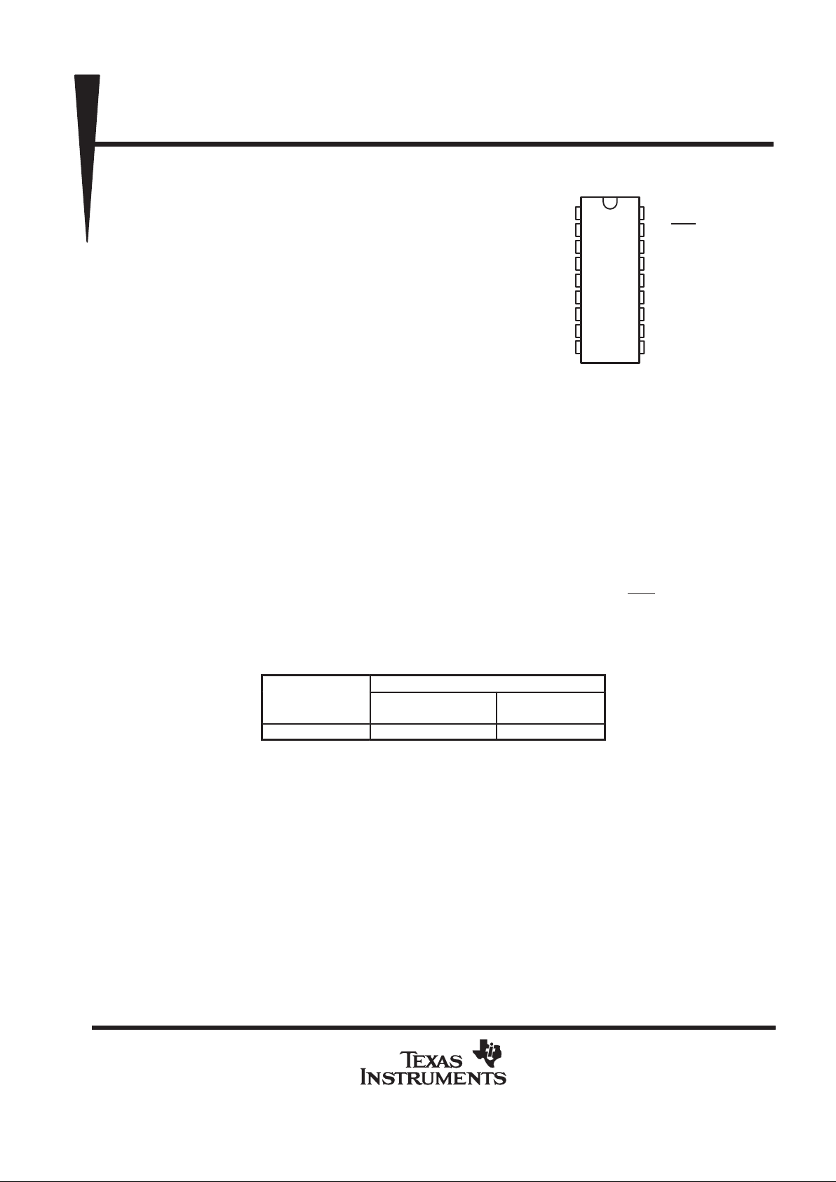
1
2
3
4
5
6
7
8
9
18
17
16
15
14
13
12
11
10
V
DD+
BIAS
R1IN
D1OUT
R2IN
D2OUT
R3IN
D3OUT
V
DD–
V
CC
ON/OFF
R1OUT
D1IN
R2OUT
D2IN
R3OUT
D3IN
GND
DW OR N PACKAGE
(TOP VIEW)
PRODUCTION DATA information is current as of publication date.
Products conform to specifications per the terms of Texas Instruments
standard warranty. Production processing does not necessarily include
testing of all parameters.
LT1039
TRIPLE EIA-232 LINE TRANSCEIVER
SLLS105B – D3627, FEBRUARY 1991 – REVISED JANUARY 1992
POST OFFICE BOX 655303 • DALLAS, TEXAS 75265
2–2
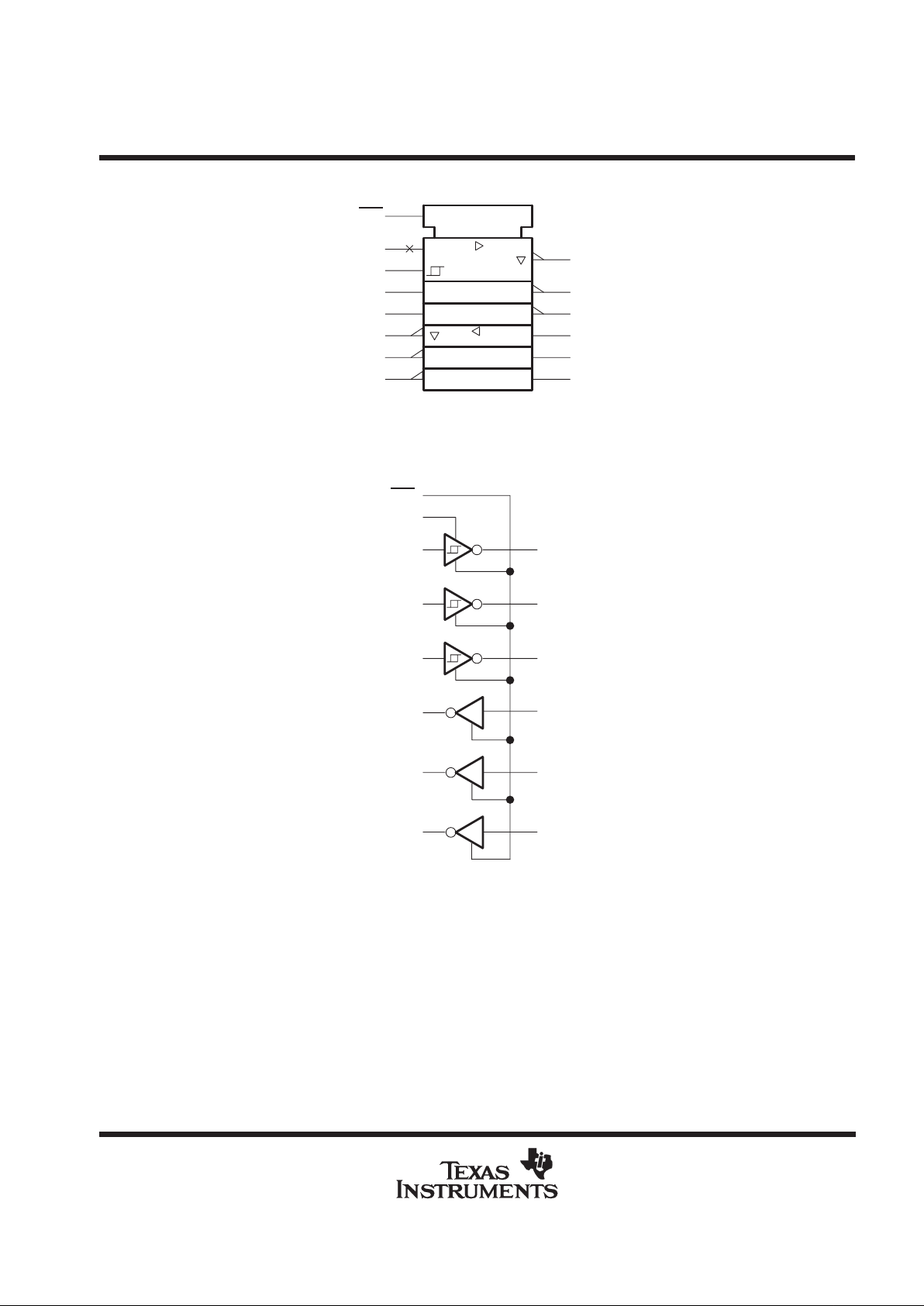
logic symbol
†
11
13
15
12
14
16
D3IN
D2IN
D1IN
R3OUT
R2OUT
R1OUT
2
8
6
4
7
5
3
D2OUT
BIAS
17
D3OUT
D1OUT
R3IN
R2IN
R1IN
ON/OFF
EN
†
This symbol is in accordance with ANSI/IEEE Std 91-1984 and IEC Publication 617-12.
logic diagram
11
D2IN
D3IN
8
D3OUT
D2OUT
D1IN
R3OUT
R2OUT
R1OUT
13
15
12
14
16
D1OUT
R3IN
6
4
7
5
3
R2IN
R1IN
2
BIAS
17
ON/OFF
LT1039
TRIPLE EIA-232 LINE TRANSCEIVER
SLLS105B – D3627, FEBRUARY 1991 – REVISED JANUARY 1992
POST OFFICE BOX 655303 • DALLAS, TEXAS 75265
2–3
Terminal Functions
PIN
NAME NO.
DESCRIPTION
BIAS 2 Keeps receiver 1 alive while the LT1039 is in the shutdown mode. Leave BIAS open when not in use.
D1IN, D2IN, D3IN 15, 13,11Line driver inputs. Operate properly on TTL or CMOS levels. Output valid from VI = (V
DD–
) + (2 to 15 V).
Connect to 5 V when not used.
D1OUT, D2OUT,
D3OUT
4, 6, 8 Line driver outputs
GND 10 Ground
ON/OFF 17 Shuts down entire circuit. Cannot be left open. If VIL is at or near 0.8 V , significant settling time may be required.
R1IN, R2IN, R3IN 3, 5, 7 Receiver inputs. Input impedance is normally 30 kΩ. Accepts EIA-232 voltage levels and has 0.4 V of
hysteresis to provide noise immunity.
R1OUT, R2OUT,
R3OUT
16, 14,12Receiver outputs with TTL/CMOS voltage levels
V
DD+
1 Positive supply voltage for driver
V
DD–
9 Negative supply voltage for driver
V
CC
18 5-V supply voltage for receivers
absolute maximum ratings over operating free-air temperature range (unless otherwise noted)
Supply voltage range, V
DD+
(see Note 1) 0 V to 15 V. . . . . . . . . . . . . . . . . . . . . . . . . . . . . . . . . . . . . . . . . . . . . . .
Supply voltage range, V
DD–
0 V to –15 V. . . . . . . . . . . . . . . . . . . . . . . . . . . . . . . . . . . . . . . . . . . . . . . . . . . . . . . . .
Supply voltage, V
CC
7 V. . . . . . . . . . . . . . . . . . . . . . . . . . . . . . . . . . . . . . . . . . . . . . . . . . . . . . . . . . . . . . . . . . . . . . . .
Input voltage range, driver input V
DD–
to 25 V. . . . . . . . . . . . . . . . . . . . . . . . . . . . . . . . . . . . . . . . . . . . . . . . . . . . . .
receiver input ±30 V. . . . . . . . . . . . . . . . . . . . . . . . . . . . . . . . . . . . . . . . . . . . . . . . . . . . . . . . .
Input voltage range, ON/OFF
0 V to 12 V. . . . . . . . . . . . . . . . . . . . . . . . . . . . . . . . . . . . . . . . . . . . . . . . . . . . . . . . . .
Output voltage range, driver output V
DD+
–30 V to V
DD–
+ 30 V. . . . . . . . . . . . . . . . . . . . . . . . . . . . . . . . . . . . .
Duration of output short circuit at (or below) T
A
= 25°C (to ±30 V, see Note 2) unlimited. . . . . . . . . . . . . . . . .
Continuous total dissipation See Dissipation Rating Table. . . . . . . . . . . . . . . . . . . . . . . . . . . . . . . . . . . . . . . . . . .
Operating free-air temperature range, T
A
0°C to 70°C. . . . . . . . . . . . . . . . . . . . . . . . . . . . . . . . . . . . . . . . . . . . .
Storage temperature range –65°C to 150°C. . . . . . . . . . . . . . . . . . . . . . . . . . . . . . . . . . . . . . . . . . . . . . . . . . . . . . .
Lead temperature 1,6 mm (1/16 inch) from case for 10 seconds 260°C. . . . . . . . . . . . . . . . . . . . . . . . . . . . . . .
NOTES: 1. All voltage values, except differential voltages, are with respect to the GND terminal.
2. The output may be shorted to either supply. Temperature and/or supply voltages must be limited to ensure that the maximum
dissipation rating is not exceeded.
DISSIPATION RATING TABLE
PACKAGE
TA ≤ 25°C
POWER RATING
DERATING FACTOR
ABOVE TA = 25°C
TA = 70°C
POWER RATING
DW 1025 mW 8.2 mW/°C 656 mW
N 1150 mW 9.2 mW/°C 736 mW

LT1039
TRIPLE EIA-232 LINE TRANSCEIVER
SLLS105B – D3627, FEBRUARY 1991 – REVISED JANUARY 1992
POST OFFICE BOX 655303 • DALLAS, TEXAS 75265
2–4
recommended operating conditions
MIN NOM MAX UNIT
Supply voltage, V
DD+
5 12 15 V
Supply voltage, V
DD–
–5 –12 –15 V
Supply voltage, V
CC
4.75 5 5.25 V
High-level input voltage, VIH (see Note 3) 2 V
Low-level input voltage, VIL (see Note 3) 0.8 V
Operating free-air temperature, T
A
0 70 °C
NOTE 3: VIH and VIL specifications apply only for inputs D1IN to D3IN.
DRIVER SECTION
electrical characteristics over recommended operating free-air temperature range, V
DD
±
=
±11.4 V
to
±12.6 V, ON/OFF at 2.5 V (unless otherwise noted)
PARAMETER TEST CONDITIONS MIN TYP
†
MAX UNIT
V
OM+
Maximum positive peak output
voltage swing
V
DD+
–0.4 V
DD+
–0.4
V
OM–
Maximum negative peak output
voltage swing
Load
= 3 kΩ to
GND
V
DD–
+1.0 V
DD–
+1.5
V
I
IH
High-level input current VI ≥ 2 V 1 20 µA
I
IL
Low-level input current VI ≤ 0.8 V 5 20 µA
VI = 0 15
VI = 5 V 80
Sourcing current, VO = 0 5 15
Sinking current, VO = 0 –5 –15
I
OZ
Off-state output current VO = ±18 V , VI = 0, ON/OFF at 0.4 V ±10 ±200 µA
I
CC
Supply current IO = 0 4 8 mA
I
CC(off)
Off-state supply current ON/OFF at 0.4 V 1 100 µA
SR Slew rate RL = 3 kΩ, CL = 51 pF 4 15 30 V/µs
†
All typical values are at V
DD±
= ±12 V , TA = 25°C.

LT1039
TRIPLE EIA-232 LINE TRANSCEIVER
SLLS105B – D3627, FEBRUARY 1991 – REVISED JANUARY 1992
POST OFFICE BOX 655303 • DALLAS, TEXAS 75265
2–5
RECEIVER SECTION
electrical characteristics over recommended ranges of supply voltage and operating free-air
temperature, ON/OFF
at 2.5 V (unless otherwise noted)
PARAMETER TEST CONDITIONS MIN TYP†MAX UNIT
V
T–
Negative-going input threshold voltage 0.5 1.3 V
V
T+
Positive-going input threshold voltage 1.7 2.8 V
V
hys
Hysteresis (VT+ – VT–) 0.1 0.4 1 V
V
OL
Low-level output voltage IO = –1.6 mA 0.4 0.5 V
V
OH
High-level output voltage IO = 160 µA 3.5 4.8 V
p
Sinking current, VO = V
CC
–10
IOSShort-circuit output current
Sourcing current, VO = 0 0.5 1
mA
I
OZ
Off-state (high-impedance state)
output current
VO = 0 to VCC, VI = 0, ON/OFF at 0.4 V ±1 ±10 µA
I
CC
Supply current IO = 0 4 7 mA
I
CC(off)
Off-state supply current ON/OFF at 0.4 V 1 100 µA
†
All typical values ground are at VCC = 5 V, TA = 25°C.

LT1039
TRIPLE EIA-232 LINE TRANSCEIVER
SLLS105B – D3627, FEBRUARY 1991 – REVISED JANUARY 1992
POST OFFICE BOX 655303 • DALLAS, TEXAS 75265
2–6

IMPORTANT NOTICE
T exas Instruments (TI) reserves the right to make changes to its products or to discontinue any semiconductor
product or service without notice, and advises its customers to obtain the latest version of relevant information
to verify, before placing orders, that the information being relied on is current and complete.
TI warrants performance of its semiconductor products and related software to the specifications applicable at
the time of sale in accordance with TI’s standard warranty. Testing and other quality control techniques are
utilized to the extent TI deems necessary to support this warranty. Specific testing of all parameters of each
device is not necessarily performed, except those mandated by government requirements.
Certain applications using semiconductor products may involve potential risks of death, personal injury, or
severe property or environmental damage (“Critical Applications”).
TI SEMICONDUCTOR PRODUCTS ARE NOT DESIGNED, INTENDED, AUTHORIZED, OR WARRANTED
TO BE SUITABLE FOR USE IN LIFE-SUPPORT APPLICATIONS, DEVICES OR SYSTEMS OR OTHER
CRITICAL APPLICATIONS.
Inclusion of TI products in such applications is understood to be fully at the risk of the customer. Use of TI
products in such applications requires the written approval of an appropriate TI officer. Questions concerning
potential risk applications should be directed to TI through a local SC sales office.
In order to minimize risks associated with the customer’s applications, adequate design and operating
safeguards should be provided by the customer to minimize inherent or procedural hazards.
TI assumes no liability for applications assistance, customer product design, software performance, or
infringement of patents or services described herein. Nor does TI warrant or represent that any license, either
express or implied, is granted under any patent right, copyright, mask work right, or other intellectual property
right of TI covering or relating to any combination, machine, or process in which such semiconductor products
or services might be or are used.
Copyright 1998, Texas Instruments Incorporated
 Loading...