

Datasheet LT1009CLPM, LT1009CLP, LT1009CDR, LT1009CD, LT1009Y Datasheet (Texas Instruments)
...
CHIP
LT1009Y
LT1009
2.5-V INTEGRATED REFERENCE CIRCUITS
SLVS013G – MAY 1987 – REVISED NOVEMBER 1999
D
Excellent Temperature Stability
D
Initial Tolerance . . . 0.2% Max
D
Dynamic Impedance . . . 0.6 Ω Max
D
Wide Operating Current Range
D
Directly Interchangeable With LM136
D
Needs No Adjustment for Minimum
Temperature Coefficient
D
Surface-Mount Three-Lead Package
description
The LT1009 reference circuit is a
precision-trimmed 2.5-V shunt regulator featuring
low dynamic impedance and a wide operating
current range. The maximum initial tolerance is
±5 mV in the LP package and ±10 mV in the
D package. The reference tolerance is achieved
by on-chip trimming, which minimizes the initial
voltage tolerance and the temperature
coefficient α
Although the LT1009 needs no adjustments, a
third terminal (ADJ) allows the reference voltage
to be adjusted ±5% to eliminate system errors. In
many applications, the LT1009 can be used as a
terminal-for-terminal replacement for the
LM136-2.5, which eliminates the external trim
network.
vz
.
ANODE
NC–No internal connection
logic symbol
ANODE CATHODE
D PACKAGE
(TOP VIEW)
NC
1
NC
2
NC
3
4
LP PACKAGE
(TOP VIEW)
ADJ
CATHODE
8
NC
7
CATHODE
6
ADJ
5
ANODE
CATHODE
ADJ
The L T1009 uses include 5-V system references, 8-bit ADC and DAC references, and power-supply monitors.
The device also can be used in applications such as digital voltmeters and current-loop measurement and
control systems.
The L T1009C is characterized for operation from 0°C to 70°C. The L T1009I is characterized for operation from
–40°C to 85°C.
AVAILABLE OPTIONS
PACKAGED DEVICES
T
A
0°C to 70°C LT1009CD LT1009CLP
–40°C to 85°C LT1009ID LT1009ILP
The D and LP packages are available taped and reeled. Add the suffix R to device
type (e.g., LT1009CDR). Chip forms are tested at 25°C.
Please be aware that an important notice concerning availability, standard warranty, and use in critical applications of
Texas Instruments semiconductor products and disclaimers thereto appears at the end of this data sheet.
SMALL
OUTLINE
(D)
PLASTIC
CYLINDRICAL
(LP)
FORM
(Y)
PRODUCTION DATA information is current as of publication date.
Products conform to specifications per the terms of Texas Instruments
standard warranty. Production processing does not necessarily include
testing of all parameters.
POST OFFICE BOX 655303 • DALLAS, TEXAS 75265
Copyright 1999, Texas Instruments Incorporated
1

LT1009
Operating free-air temperature range, T
°C
2.5-V INTEGRATED REFERENCE CIRCUITS
SLVS013G – MAY 1987 – REVISED NOVEMBER 1999
schematic
Q14 Q11
Q8
CATHODE
24 kΩ 24 kΩ 6.6 kΩ
20 pF
Q2
Q1
Q3
All component values shown are nominal.
absolute maximum ratings over operating free-air temperature range
Reverse current, I
R
Q7
10 kΩ
30 pF
Q9
Q4
Q6
Q12
Q5
720 Ω
Q10
500 Ω
30 kΩ
ADJ
6.6 kΩ
Q13
ANODE
†
20 mA. . . . . . . . . . . . . . . . . . . . . . . . . . . . . . . . . . . . . . . . . . . . . . . . . . . . . . . . . . . . . . . . . . . . . .
Forward current, IF 10 mA. . . . . . . . . . . . . . . . . . . . . . . . . . . . . . . . . . . . . . . . . . . . . . . . . . . . . . . . . . . . . . . . . . . . . . .
Package thermal impedance, θ
, (see Notes 1 and 2):D package 97°C/W. . . . . . . . . . . . . . . . . . . . . . . . . . . .
JA
LP package 156°C/W. . . . . . . . . . . . . . . . . . . . . . . . . .
Lead temperature 1,6 mm (1/16 inch) from case for 10 seconds: D and LP packages 260°C. . . . . . . . . . . . .
Storage temperature range, T
†
Stresses beyond those listed under “absolute maximum ratings” may cause permanent damage to the device. These are stress ratings only, and
functional operation of the device at these or any other conditions beyond those indicated under “recommended operating conditions” is not
implied. Exposure to absolute-maximum-rated conditions for extended periods may affect device reliability.
NOTES: 1. Maximum power dissipation is a function of T
temperature is PD = (T
2. The package thermal impedance is calculated in accordance with JESD 51.
J(max)
–65°C to 150°C. . . . . . . . . . . . . . . . . . . . . . . . . . . . . . . . . . . . . . . . . . . . . . . . . . .
stg
,
θ
– TA)/
J(max)
θ
. Operation at the absolute maximum TJ of 150°C can impact reliability.
JA
, and TA. The maximum allowable power dissipation at any allowable ambient
JA
recommended operating conditions
p
2
p
A
POST OFFICE BOX 655303 • DALLAS, TEXAS 75265
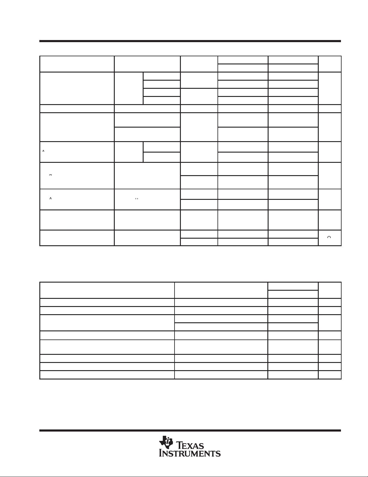
MIN MAX UNIT
LT1009C 0 70
LT1009I –40 85
°
PARAMETER
TEST CONDITIONS
T
†
UNIT
25°C
VZReference voltage
I
mA
V
Full range
Adjustment range
25°C
mV
∆V
Full range
mV
ppm/°C
∆V
I
400 µA to 10 mA
mV
I
mA
Ω
PARAMETER
TEST CONDITIONS
UNIT
Adjustment range
mV
LT1009
2.5-V INTEGRATED REFERENCE CIRCUITS
SLVS013G – MAY 1987 – REVISED NOVEMBER 1999
electrical characteristics at specified free-air temperature
A
D package
= 1
Z
V
Z(temp)
α
∆VZ/∆t
z
z
†
Full range is 0°C to 70°C for the LT1009C and –40°C to 85°C for the LT1009I.
‡
The average temperature coefficient of reference voltage is defined as the total change in reference voltage divided by the specified temperature
range.
Forward voltage IF = 2 mA 25°C 0.4 1 0.4 1 V
F
IZ = 1 mA,
V
ADJ
IZ = 1 mA,
V
ADJ
Change in
reference voltage
with temperature
Average
temperature
VZ
coefficient of
reference voltage
Change in
reference voltage
Z
with current
Long-term change
in reference
voltage
Reference
impedance
‡
=
Z
IZ = 1 mA 25°C 20 20 ppm/khr
= 1
Z
LP package
D package
LP package
= GND to V
= 0.6 V to VZ – 0.6 V
Z
D package
LP package
°
°
0°C to 70°C 15 25 30
–40°C to 85°C 20
25°C 2.6 10 2.6 6
Full range 12 10
25°C 0.3 1 0.3 1
Full range 1.4 1.4
LT1009C LT1009I
MIN TYP MAX MIN TYP MAX
2.49 2.5 2.51 2.49 2.5 2.51
2.495 2.5 2.505 2.495 2.5 2.505
2.485 2.515 2.475 2.525
2.491 2.509 2.48 2.52
125 125
45 45
5 15
4 15
pp
°
electrical characteristics at TA = 25°C
LT1009Y
MIN TYP MAX
V
Z
V
F
∆V
Z(temp)
α
VZ
∆V
Z
∆VZ/∆t Long-term change in reference voltage IZ = 1 mA 20 ppm/khr
z
z
‡
The average temperature coefficient of reference voltage is defined as the total change in reference voltage divided by the specified temperature
range.
Reference voltage IZ = 1 mA 2.49 2.5 2.51 V
Forward voltage IF = 2 mA 0.4 1 V
IZ = 1 mA, V
IZ = 1 mA, V
Change in reference voltage with temperature 2.5 mV
Average temperature coefficient of
reference voltage
Change in reference voltage with current IZ = 400 µA to 10 mA 2.6 mV
Reference impedance IZ = 1 mA 0.3 1 W
‡
= GND to V
ADJ
= 0.6 V to VZ –0.6 V 45
ADJ
Z
125
15 ppm/°C
POST OFFICE BOX 655303 • DALLAS, TEXAS 75265
3

LT1009
2.5-V INTEGRATED REFERENCE CIRCUITS
SLVS013G – MAY 1987 – REVISED NOVEMBER 1999
REFERENCE VOLTAGE
FREE-AIR TEMPERATURE
2.53
Iz = 1 mA
2.52
2.51
2.5
2.49
– Reference Voltage – V
Z
V
2.48
2.47
– 50 – 25 0 25 50 75
TA – Free-Air Temperature – °C
Figure 1
vs
TYPICAL CHARACTERISTICS
CHANGE IN REFERENCE VOLTAGE
5
4
3
2
1
– Change in Reference Voltage – mV
Z
∆V
100 125
0
048121620
†
vs
REFERENCE CURRENT
IZ – Reference Current – mA
Figure 2
REVERSE CURRENT
vs
REVERSE VOLTAGE
–1
10
–2
10
–3
10
– Reverse Current – A
R
I
–4
10
–5
10
0.6 1 1.4 1.8 2.2 2.6
TJ = 125°C
TJ = –55°C
TJ = 25°C
VR – Reverse Voltage – V
Figure 3
FORWARD VOLTAGE
vs
FORWARD CURRENT
1.2
TJ = 25°C
1
0.8
0.6
0.4
– Forward Voltage – V
F
V
0.2
0
0.001 0.01 0.1 1 10
IF – Forward Current– mA
Figure 4
†
Data at high and low temperatures are applicable only within the rated operating free-air temperature ranges of the various devices.
4
POST OFFICE BOX 655303 • DALLAS, TEXAS 75265

LT1009
2.5-V INTEGRATED REFERENCE CIRCUITS
SLVS013G – MAY 1987 – REVISED NOVEMBER 1999
TYPICAL CHARACTERISTICS
REFERENCE IMPEDANCE
vs
FREQUENCY
100
Iz = 1 mA
TJ = –55°C to 125°C
10
1
– Reference Impedance – Ω
z
z
0.1
0.01 0.1 1 10 100
f – Frequency – kHz
Figure 5
3.5
3
2.5
2
1.5
1
0.5
0
250
Iz = 1 mA
TJ = 25°C
200
nV/ Hz– Noise Voltage –
150
100
n
V
50
10 100 1 k 10 k 100 k
TRANSIENT RESPONSE
Output
5 kΩ
Input
NOISE VOLTAGE
vs
FREQUENCY
f – Frequency – Hz
Figure 6
Input and Output Voltages – V
8
4
0
POST OFFICE BOX 655303 • DALLAS, TEXAS 75265
Output
Input
01
t – Time – µs
Figure 7
20
5

LT1009
2.5-V INTEGRATED REFERENCE CIRCUITS
SLVS013G – MAY 1987 – REVISED NOVEMBER 1999
APPLICATION INFORMATION
5 V to 35 V
LT1009
†
This does not affect temperature coefficient. It provides ±5% trim range.
Figure 8. 2.5-V Reference
3.6 V to 40 V
V+
LM334
V–
3.6 kΩ
Output
†
10 kΩ
Trim
R
62 Ω
LT1009
10 kΩ
Figure 9. Adjustable Reference With Wide Supply Range
LT1084
V
I
10 µF
ADJ
OUTIN
10 µF
LT1009
1.2 kΩ
V
374 Ω
2 kΩ
O
Figure 10. Power Regulator With Low Temperature Coefficient
6
POST OFFICE BOX 655303 • DALLAS, TEXAS 75265

LT1009
2.5-V INTEGRATED REFERENCE CIRCUITS
SLVS013G – MAY 1987 – REVISED NOVEMBER 1999
APPLICATION INFORMATION
5 V
5.1 kΩ
5 V
–5 V
5.1 kΩ
LT1009
5 kΩ
–5 V
10 kΩ
1%
9.76 kΩ
1%
500 Ω
Figure 11. Switchable ±1.25-V Bipolar Reference
1 µF
10 kΩ
VI ≥ 6 V
1 kΩ
100 kΩ
1 kΩ10 kΩ
+
20 µF
–
+
LT1001C
Output
2.5 V
LT1009
+
20 µF
Figure 12. Low-Noise 2.5-V Buffered Reference
POST OFFICE BOX 655303 • DALLAS, TEXAS 75265
7

IMPORTANT NOTICE
T exas Instruments and its subsidiaries (TI) reserve the right to make changes to their products or to discontinue
any product or service without notice, and advise customers to obtain the latest version of relevant information
to verify, before placing orders, that information being relied on is current and complete. All products are sold
subject to the terms and conditions of sale supplied at the time of order acknowledgement, including those
pertaining to warranty, patent infringement, and limitation of liability.
TI warrants performance of its semiconductor products to the specifications applicable at the time of sale in
accordance with TI’s standard warranty. Testing and other quality control techniques are utilized to the extent
TI deems necessary to support this warranty . Specific testing of all parameters of each device is not necessarily
performed, except those mandated by government requirements.
CERTAIN APPLICA TIONS USING SEMICONDUCT OR PRODUCTS MAY INVOLVE POTENTIAL RISKS OF
DEATH, PERSONAL INJURY, OR SEVERE PROPERTY OR ENVIRONMENTAL DAMAGE (“CRITICAL
APPLICATIONS”). TI SEMICONDUCTOR PRODUCTS ARE NOT DESIGNED, AUTHORIZED, OR
WARRANTED TO BE SUITABLE FOR USE IN LIFE-SUPPORT DEVICES OR SYSTEMS OR OTHER
CRITICAL APPLICA TIONS. INCLUSION OF TI PRODUCTS IN SUCH APPLICATIONS IS UNDERST OOD TO
BE FULLY AT THE CUSTOMER’S RISK.
In order to minimize risks associated with the customer’s applications, adequate design and operating
safeguards must be provided by the customer to minimize inherent or procedural hazards.
TI assumes no liability for applications assistance or customer product design. TI does not warrant or represent
that any license, either express or implied, is granted under any patent right, copyright, mask work right, or other
intellectual property right of TI covering or relating to any combination, machine, or process in which such
semiconductor products or services might be or are used. TI’s publication of information regarding any third
party’s products or services does not constitute TI’s approval, warranty or endorsement thereof.
Copyright 1999, Texas Instruments Incorporated
 Loading...