

Page 1
0
0.05
0.1
0.15
0.2
0.25
0.3
0.35
0.4
0.45
−50 −25 0 25 50 75 100 125 150
VO= 3.3 V
C
byp
= 10 nF
Dropout − (V)
150 mA
50 mA
10 mA
1 mA
Temperature − ( C)°
Product
Folder
Sample &
Buy
Technical
Documents
Tools &
Software
Support &
Community
LP2985 150-mA Low-noise Low-dropout Regulator With Shutdown
1 Features 3 Description
1
• Output Tolerance of
– 1% (A Grade)
– 1.5% (Standard Grade)
• Ultra-Low Dropout, Typically
– 280 mV at Full Load of 150 mA
– 7 mV at 1 mA
• Wide VINRange: 16 V Max
• Low IQ: 850 μA at Full Load at 150 mA
• Shutdown Current: 0.01 μA Typ
• Low Noise: 30 μV
With 10-nF Bypass
RMS
Capacitor
• Stable With Low-ESR Capacitors, Including
Ceramic
• Overcurrent and Thermal Protection
• High Peak-Current Capability
• ESD Protection Exceeds JESD 22
– 2000-V Human-Body Model (A114-A)
– 200-V Machine Model (A115-A)
The LP2985 family of fixed-output, low-dropout
regulators offers exceptional, cost-effective
performance for both portable and nonportable
applications. Available in voltages of 1.8 V, 2.5 V, 2.8
V, 2.9 V, 3 V, 3.1 V, 3.3 V, 5 V, and 10 V, the family
has an output tolerance of 1% for the A version (1.5%
for the non-A version) and is capable of delivering
150-mA continuous load current. Standard regulator
features, such as overcurrent and overtemperature
protection, are included.
PART NUMBER PACKAGE BODY SIZE (NOM)
LP2985 SOT-23 (5) 2.90 mm x 1.60 mm
(1) For all available packages, see the orderable addendum at
the end of the data sheet.
Dropout Voltage vs Temperature
LP2985
SLVS522O –JULY 2004–REVISED JANUARY 2015
Device Information
(1)
2 Applications
• Portable Devices
• Digital Cameras and Camcorders
• CD Players
• MP3 Players
1
An IMPORTANT NOTICE at the end of this data sheet addresses availability, warranty, changes, use in safety-critical applications,
intellectual property matters and other important disclaimers. PRODUCTION DATA.
Page 2

LP2985
SLVS522O –JULY 2004–REVISED JANUARY 2015
www.ti.com
Table of Contents
1 Features.................................................................. 1
2 Applications ........................................................... 1
3 Description............................................................. 1
4 Revision History..................................................... 2
5 Pin Configuration and Functions......................... 3
6 Specifications......................................................... 4
6.1 Absolute Maximum Ratings ..................................... 4
6.2 ESD Ratings.............................................................. 4
6.3 Recommended Operating Conditions...................... 4
6.4 Thermal Information.................................................. 4
6.5 Electrical Characteristics.......................................... 5
6.6 Typical Characteristics.............................................. 7
7 Detailed Description............................................ 11
7.1 Overview................................................................. 11
7.2 Functional Block Diagram ....................................... 11
7.3 Feature Description................................................. 11
7.4 Device Functional Modes........................................ 11
8 Application and Implementation ........................ 12
8.1 Application Information............................................ 12
9 Power Supply Recommendations...................... 16
10 Layout................................................................... 17
10.1 Layout Guidelines................................................. 17
10.2 Layout Example.................................................... 17
11 Device and Documentation Support................. 17
11.1 Trademarks........................................................... 17
11.2 Electrostatic Discharge Caution............................ 17
11.3 Glossary................................................................ 17
12 Mechanical, Packaging, and Orderable
Information........................................................... 17
4 Revision History
Changes from Revision N (June 2011) to Revision O Page
• Added Applications, Device Information table, Pin Functions table, ESD Ratings table, Thermal Information table,
Feature Description section, Device Functional Modes, Application and Implementation section, Power Supply
Recommendations section, Layout section, Device and Documentation Support section, and Mechanical,
Packaging, and Orderable Information section. ..................................................................................................................... 1
• Deleted Ordering Information table. ....................................................................................................................................... 1
2 Submit Documentation Feedback Copyright © 2004–2015, Texas Instruments Incorporated
Page 3

DBV (SOT-23) PACKAGE
(TOP VIEW)
1
2
3
5
4
V
IN
GND
ON/OFF
V
OUT
BYPASS
LP2985
www.ti.com
SLVS522O –JULY 2004–REVISED JANUARY 2015
5 Pin Configuration and Functions
Pin Functions
PIN
NAME NO.
BYPASS 4 I/O Attach a 10-nF capacitor to improve low-noise performance.
GND 2 — Ground
ON/OFF 3 I Active-low shutdown pin. Tie to VINif unused.
V
IN
V
OUT
1 I Supply input
5 O Voltage output
TYPE DESCRIPTION
Copyright © 2004–2015, Texas Instruments Incorporated Submit Documentation Feedback 3
Page 4
LP2985
SLVS522O –JULY 2004–REVISED JANUARY 2015
www.ti.com
6 Specifications
6.1 Absolute Maximum Ratings
over virtual junction temperature range (unless otherwise noted)
V
IN
V
ON/ OFF
I
O
θ
JA
T
J
T
stg
Continuous input voltage range
ON/OFF input voltage range –0.3 16 V
Output voltage range
Output current
(3)
(4)
Package thermal impedance
Operating virtual junction temperature 150 °C
Storage temperature range –65 150 °C
(1) Stresses beyond those listed under "absolute maximum ratings" may cause permanent damage to the device. These are stress ratings
only, and functional operation of the device at these or any other conditions beyond those indicated under Recommended Operating
Conditions is not implied. Exposure to absolute-maximum-rated conditions for extended periods may affect device reliability.
(2) The PNP pass transistor has a parasitic diode connected between the input and output. This diode normally is reverse biased
(VIN> V
more details).
), but will be forward biased if the output voltage exceeds the input voltage by a diode drop (see Application Information for
OUT
(3) If load is returned to a negative power supply in a dual-supply system, the output must be diode clamped to GND.
(4) Maximum power dissipation is a function of TJ(max), θJA, and TA. The maximum allowable power dissipation at any allowable ambient
temperature is PD= (TJ(max) – TA)/θJA. Operating at the absolute maximum TJof 150°C can affect reliability.
(5) The package thermal impedance is calculated in accordance with JESD 51-7.
(2)
(4) (5)
(1)
MIN MAX UNIT
–0.3 16 V
–0.3 9 V
Internally limited
(short-circuit protected)
—
206 °C/W
6.2 ESD Ratings
VALUE UNIT
(1)
2000
1000
V
(ESD)
Human body model (HBM), per ANSI/ESDA/JEDEC JS-001, all pins
Electrostatic discharge V
Charged device model (CDM), per JEDEC specification JESD22-C101,
(2)
all pins
(1) JEDEC document JEP155 states that 500-V HBM allows safe manufacturing with a standard ESD control process.
(2) JEDEC document JEP157 states that 250-V CDM allows safe manufacturing with a standard ESD control process.
6.3 Recommended Operating Conditions
MIN MAX UNIT
V
IN
V
ON/ OFF
I
OUT
T
J
Supply input voltage 2.2
ON/OFF input voltage 0 V
Output current 150 mA
Virtual junction temperature –40 125 °C
(1) Recommended minimum VINis the greater of 2.5 V or V
+ rated dropout voltage (max) for operating IL.
OUT(max)
(1)
16 V
IN
6.4 Thermal Information
LP2985
THERMAL METRIC
R
θJA
Junction-to-ambient thermal resistance 206 °C/W
(1) For more information about traditional and new thermal metrics, see the IC Package Thermal Metrics application report, SPRA953.
(1)
DBV UNIT
5 PINS
V
4 Submit Documentation Feedback Copyright © 2004–2015, Texas Instruments Incorporated
Page 5
LP2985
www.ti.com
6.5 Electrical Characteristics
at specified virtual junction temperature range, VIN= V
(unless otherwise noted)
PARAMETER TEST CONDITIONS T
IL= 1 mA 25°C –1 1 –1.5 1.5
ΔV
OUT
VIN– V
I
GND
V
ON/ OFF
I
ON/ OFF
Output voltage
tolerance
Line regulation VIN= [V
Dropout voltage
OUT
(1)
GND pin current μA
ON/OFF input voltage
ON/OFF input current μA
1 mA ≤ IL≤ 50 mA
1 mA ≤ IL≤ 150 mA
+ 1 V] to 16 V %/V
OUT(NOM)
IL= 0
IL= 1 mA
IL= 10 mA mV
IL= 50 mA
IL= 150 mA
IL= 0
IL= 1 mA 25°C (LP2985-10) 140 140
IL= 10 mA 25°C (LP2985-10) 250 250
IL= 50 mA 25°C (LP2985-10) 650 650
IL= 150 mA 25°C (LP2985-10) 1800 1800
V
< 0.3 V (OFF) 25°C 0.01 0.8 0.01 0.8
ON/ OFF
V
< 0.15 V (OFF)
ON/ OFF
V
= HIGH → O/P ON
ON/ OFF
(2)
V
= LOW → O/P OFF
ON/ OFF
V
= 0
ON/ OFF
V
= 5 V
ON/ OFF
SLVS522O –JULY 2004–REVISED JANUARY 2015
OUT(NOM)
+ 1 V, V
J
= 2 V, CIN= 1 μF, IL= 1 mA, C
ON/ OFF
LP2985A-xx LP2985-xx
MIN TYP MAX MIN TYP MAX
25°C –1.5 1.5 –2.5 2.5
–40°C to 125°C –2.5 2.5 –3.5 3.5 %V
25°C –2.5 2.5 –3 3
–40°C to 125°C –3.5 3.5 –4 4
25°C 0.007 0.014 0.007 0.014
–40°C to 125°C 0.032 0.032
25°C 1 3 1 3
–40°C to 125°C 5 5
25°C 7 10 7 10
–40°C to 125°C 15 15
25°C 40 60 40 60
–40°C to 125°C 90 90
25°C 120 150 120 150
–40°C to 125°C 225 225
25°C 280 350 280 350
–40°C to 125°C 575 575
25°C 65 95 65 95
25°C (LP2985-10) 125 125
–40°C to 125°C 125 125
–40°C to 125°C
(LP2985-10)
160 160
25°C 75 110 75 110
–40°C to 125°C 170 170
25°C 120 220 120 220
–40°C to 125°C 400 400
25°C 350 600 350 600
–40°C to 125°C 1000 1000
25°C 850 1500 850 1500
–40°C to 125°C 2500 2500
–40°C to 105°C 0.05 2 0.05 2
–40°C to 125°C 5 5
25°C 1.4 1.4
–40°C to 125°C 1.6 1.6
25°C 0.55 0.55
–40°C to 125°C 0.15 0.15
25°C 0.01 0.01
–40°C to 125°C –2 –2
25°C 5 5
–40°C to 125°C 15 15
OUT
= 4.7 μF
UNIT
NOM
V
(1) Dropout voltage is defined as the input-to-output differential at which the output voltage drops 100 mV below the value measured with a
1-V differential.
(2) The ON/OFF input must be driven properly for reliable operation (see Application Information).
Copyright © 2004–2015, Texas Instruments Incorporated Submit Documentation Feedback 5
Page 6
LP2985
SLVS522O –JULY 2004–REVISED JANUARY 2015
Electrical Characteristics (continued)
at specified virtual junction temperature range, VIN= V
(unless otherwise noted)
PARAMETER TEST CONDITIONS T
V
n
ΔV
OUT
ΔV
IN
I
OUT(PK)
I
OUT(SC)
Output noise (RMS) C
/ f = 1kHz, C
Ripple rejection 25°C 45 45 dB
Peak output current V
Short-circuit current RL= 0 (steady state)
(3) See Figure 6 in Typical Performance Characteristics.
BW = 300 Hz to 50 kHz,
= 10 μF, 25°C 30 30 μV
OUT
C
= 10 nF
BYPASS
= 10 μF,
≥ V
OUT
= 10 nF
– 5% 25°C 350 350 mA
O(NOM)
(3)
C
BYPASS
OUT
OUT(NOM)
+ 1 V, V
J
= 2 V, CIN= 1 μF, IL= 1 mA, C
ON/ OFF
LP2985A-xx LP2985-xx
MIN TYP MAX MIN TYP MAX
OUT
25°C 400 400 mA
www.ti.com
= 4.7 μF
UNIT
6 Submit Documentation Feedback Copyright © 2004–2015, Texas Instruments Incorporated
Page 7
200
220
240
260
280
300
320
0 0.5 1 1.5 2 2.5 3 3.5
Output Voltage − (V)
I
SC
− (mA)
VO= 3.3 V
−100
100 300 500 700
Time − (ms)
VI= 16 V
VO= 3.3 V
Ci= 1 mF
C
byp
= 0.01 mF
Short-Circuit Current −
(A)
0
0.05
0.1
0.15
0.2
0.25
0.3
0.35
0.4
0.45
0.5
0
0.05
0.1
0.15
0.2
0.25
0.3
0.35
0.4
0.45
0.5
−500
0 500 1000 1500 2000
Time − (ms)
Short-Circuit Current −
(A)
VI= 6 V
VO= 3.3 V
Ci= 1 mF
C
byp
= 0.01 mF
0
0.05
0.1
0.15
0.2
0.25
0.3
0.35
0.4
0.45
−50 −25 0 25 50 75 100 125 150
VO= 3.3 V
C
byp
= 10 nF
Dropout − (V)
150 mA
50 mA
10 mA
1 mA
Temperature − ( C)°
9.85
9.90
9.95
10.00
10.05
10.10
10.15
10.20
-50 -25 0 25 50 75 100 125 150
Temperature – °C
Outp ut Voltage – V
VI= 11 V
VO= 10 V
CI= 1 µF
CO= 4.7 µF
IO= 1 mA
3.295
3.305
3.315
3.325
3.335
3.345
−50 −25
0 25 50 75 100 125 150
Output V
oltage − (V)
VI= 4.3 V
VO= 3.3 V
Ci= 1 mF
Co= 4.7 mF
IO= 1 mA
Temperature − ( C)°
LP2985
www.ti.com
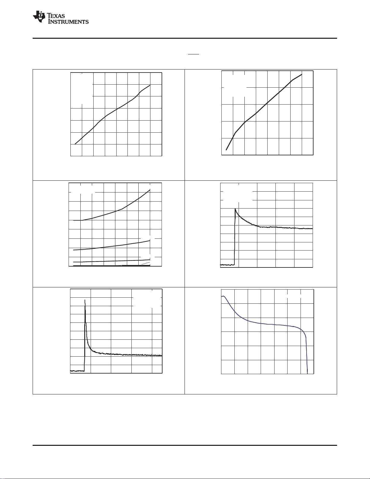
6.6 Typical Characteristics
CIN= 1 μF, C
= 4.7 μF, VIN= V
OUT
OUT(NOM)
Figure 1. Output Voltage vs Temperature
SLVS522O –JULY 2004–REVISED JANUARY 2015
+ 1 V, TA= 25°C, ON/OFF pin tied to VIN(unless otherwise specified)
Figure 2. Output Voltage vs Temperature
Figure 3. Dropout Voltage vs Temperature
Copyright © 2004–2015, Texas Instruments Incorporated Submit Documentation Feedback 7
Figure 5. Short-circuit Current vs Time
Figure 4. Short-circuit Current vs Time
Figure 6. Short-circuit Current vs Output Voltage
Page 8
0.001
0.01
0.1
1
10
10 100 1k 10k 100k 1M
Frequency − (Hz)
Ci= 1 mF
Co= 10 mF
VO= 3.3 V
10 mA
100 mA
1 mA
Output Impedance −
W( )
0
10
20
30
40
50
60
70
80
90
100
10 100 1k 10k 100k 1M
Frequency − (Hz)
Ripple Rejection − (dB)
VI= 5 V
VO= 3.3 V
Co= 4.7 mF
C
byp
= 10 nF
10 mA
100 mA
1 mA
0
10
20
30
40
50
60
70
80
90
100
10 100 1k 10k 100k 1M
Frequency − (Hz)
Ripple Rejection − (dB)
50 mA
150 mA
1 mA
VI= 3.7 V
VO= 3.3 V
Co= 10 mF
C
byp
= 0 nF
0
10
20
30
40
50
60
70
80
90
100
10 100 1k 10k 100k 1M
Frequency − (Hz)
Ripple Rejection − (dB)
VI= 5 V
VO= 3.3 V
Co= 4.7 mF
C
byp
= 10 nF
50 mA
150 mA
1 mA
0
10
20
30
40
50
60
70
80
90
100
10 100 1k 10k 100k 1M
Frequency − (Hz)
Ripple Rejection − (dB)
VI= 5 V
VO= 3.3 V
Co= 10 mF
C
byp
= 0 nF
50 mA
150 mA
1 mA
0
100
200
300
400
500
600
700
800
900
1000
1100
1200
0
20 40 60 80 100 120 140
Load Current − mA
160
VO= 3.3 V
C
byp
= 10 nF
Ground Pin Current −
mA
LP2985
SLVS522O –JULY 2004–REVISED JANUARY 2015
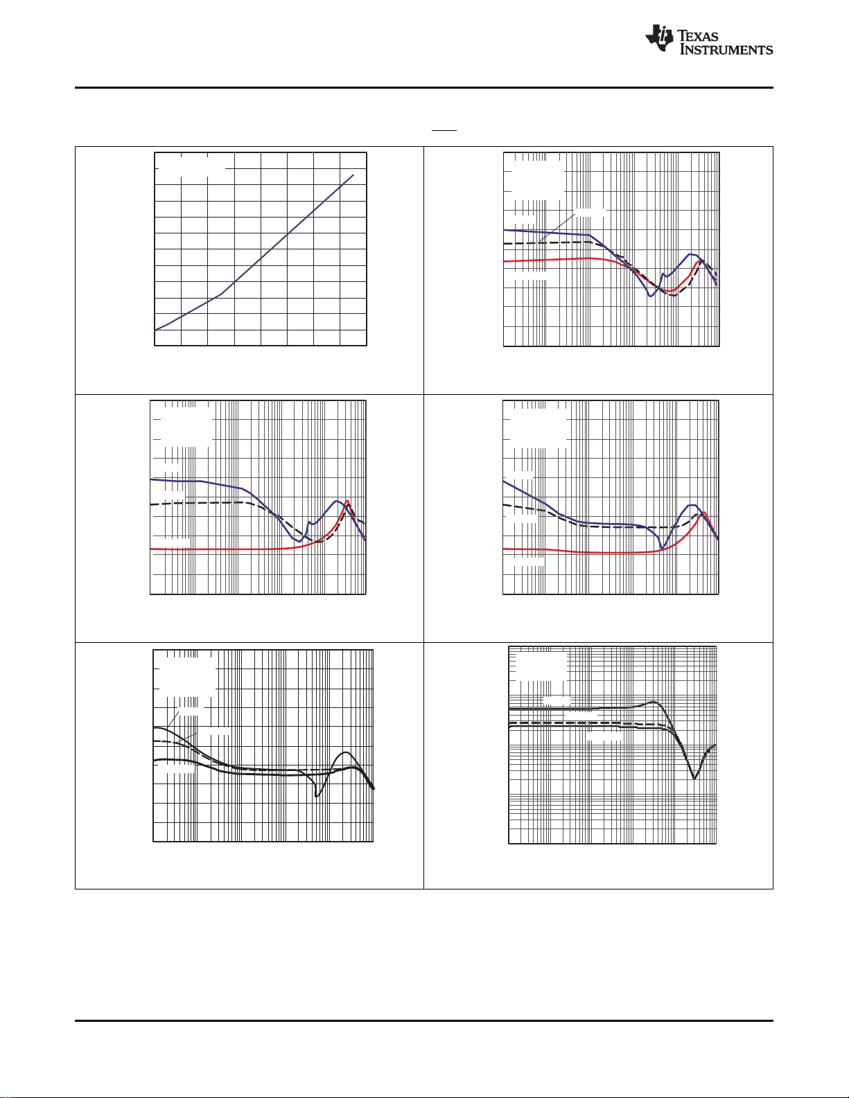
Typical Characteristics (continued)
CIN= 1 μF, C
= 4.7 μF, VIN= V
OUT
OUT(NOM)
+ 1 V, TA= 25°C, ON/OFF pin tied to VIN(unless otherwise specified)
Figure 7. Ground Pin Current vs Load Current
www.ti.com
Figure 8. Ripple Rejection vs Frequency
Figure 9. Ripple Rejection vs Frequency Figure 10. Ripple Rejection vs Frequency
8 Submit Documentation Feedback Copyright © 2004–2015, Texas Instruments Incorporated
Figure 11. Ripple Rejection vs Frequency
Figure 12. Output Impedance vs Frequency
Page 9
0
200
400
600
800
1000
1200
1400
−50 −25 0 25 50 75 100 125
150
Ground Current − (C)
0 mA
Temperature − (°C)
150 mA
50 mA
10 mA
1 mA
VO= 3.3 V
C
byp
= 10 nF
0
0.2
0.4
0.6
0.8
1
1.2
1.4
1.6
1.8
0 1 2 3 4 5 6
Input Voltage − (V)
Input Current − (mA)
RL= Open
RL= 3.3 kW
VO= 3.3 V
C
byp
= 10 nF
0.01
0.1
1
10
100 1k 10k 100k
Frequency − (Hz)
Noise Density −
( V/m
I
LOAD
= 1 mA
C
byp
= 1 nF
C
byp
= 10 nF
C
byp
= 100 pF
Hz)
0.001
0.01
0.1
1
10
10 100 1k 10k 100k
1M
Frequency − (Hz)
Ci= 1 mF
Co= 4.7 mF
VO= 3.3 V
10 mA
100 mA
1 mA
Output Impedance −
W( )
0.01
0.1
1
10
100 1k 10k 100k
Frequency − (Hz)
Noise Density −
m( V/
C
byp
= 1 nF
C
byp
= 10 nF
C
byp
= 100 pF
I
LOAD
= 150 mA
Hz)
LP2985
www.ti.com
Typical Characteristics (continued)
CIN= 1 μF, C
= 4.7 μF, VIN= V
OUT
OUT(NOM)
+ 1 V, TA= 25°C, ON/OFF pin tied to VIN(unless otherwise specified)
Figure 13. Output Impedance vs Frequency
SLVS522O –JULY 2004–REVISED JANUARY 2015
Figure 14. Output Noise Density vs Frequency
Figure 15. Output Noise Density vs Frequency
Copyright © 2004–2015, Texas Instruments Incorporated Submit Documentation Feedback 9
Figure 17. Ground-pin Current vs Temperature
Figure 16. Input Current vs Input Voltage
Figure 18. 2.2-μF Stable ESR Range
for Output Voltage ≤ 2.3 V
Page 10

LP2985
SLVS522O –JULY 2004–REVISED JANUARY 2015
Typical Characteristics (continued)
CIN= 1 μF, C
= 4.7 μF, VIN= V
OUT
Figure 19. 4.7-μF Stable ESR Range
for Output Voltage ≤ 2.3 V
OUT(NOM)
+ 1 V, TA= 25°C, ON/OFF pin tied to VIN(unless otherwise specified)
www.ti.com
Figure 20. 2.2-μF/3.3-μF Stable ESR Range
for Output Voltage ≥ 2.5 V
10 Submit Documentation Feedback Copyright © 2004–2015, Texas Instruments Incorporated
Page 11

V
IN
V
OUT
ON/OFF
Overcurrent/
Overtemperature
Protection
V
REF
1.23 V
−
+
BYPASS
LP2985
www.ti.com
SLVS522O –JULY 2004–REVISED JANUARY 2015
7 Detailed Description
7.1 Overview
The LP2985 family of fixed-output, low-dropout regulators offers exceptional, cost-effective performance for both
portable and nonportable applications. Available in voltages of 1.8 V, 2.5 V, 2.8 V, 2.9 V, 3 V, 3.1 V, 3.3 V, 5 V,
and 10 V, the family has an output tolerance of 1% for the A version (1.5% for the non-A version) and is capable
of delivering 150-mA continuous load current. Standard regulator features, such as overcurrent and
overtemperature protection, are included.
7.2 Functional Block Diagram
7.3 Feature Description
The LP2985 has a host of features that makes the regulator an ideal candidate for a variety of portable
applications:
• Low dropout: A PNP pass element allows a typical dropout of 280 mV at 150-mA load current and 7 mV at 1mA load.
• Low quiescent current: The use of a vertical PNP process allows for quiescent currents that are considerably
lower than those associated with traditional lateral PNP regulators.
• Shutdown: A shutdown feature is available, allowing the regulator to consume only 0.01 μA when the
ON/OFF pin is pulled low.
• Low-ESR-capacitor friendly: The regulator is stable with low-ESR capacitors, allowing the use of small,
inexpensive, ceramic capacitors in cost-sensitive applications.
• Low noise: A BYPASS pin allows for low-noise operation, with a typical output noise of 30 μV
, with the
RMS
use of a 10-nF bypass capacitor.
• Small packaging: For the most space-constrained needs, the regulator is available in the SOT-23 package.
7.4 Device Functional Modes
7.4.1 Normal Operation
In normal operation, the device will output a fixed voltage corresponding with the orderable part number. The
device can deliver 150 mA of continuous load current.
7.4.2 Shutdown Mode
Set the ON/OFF pin low to shut down the device when VINis still present. If a shutdown mode is not needed, tie
the pin to VIN. For proper operation, do not leave ON/OFF unconnected, and apply a signal with a slew rate of
≥40 mV/μs.
Copyright © 2004–2015, Texas Instruments Incorporated Submit Documentation Feedback 11
Page 12

V
OUT
2.2 µF
10 nF
1 µF
V
IN
1
ON/OFF
2GND
3
5
4
BYPASS
LP2985
LP2985
SLVS522O –JULY 2004–REVISED JANUARY 2015
8 Application and Implementation
NOTE
Information in the following applications sections is not part of the TI component
specification, and TI does not warrant its accuracy or completeness. TI’s customers are
responsible for determining suitability of components for their purposes. Customers should
validate and test their design implementation to confirm system functionality.
8.1 Application Information
The following application schematic shows the standard usage of the LP2985 as a low-dropout regulator.
8.1.1 Typical Application
www.ti.com
8.1.2 Design Requirements
Minimum C
value for stability (can be increased without limit for improved stability and transient response)
OUT
ON/OFF must be actively terminated. Connect to VINif shutdown feature is not used.
Optional BYPASS capacitor for low-noise operation
8.1.3 Capacitors
8.1.3.1 Input Capacitor (CIN)
A minimum value of 1 μF (over the entire operating temperature range) is required at the input of the LP2985. In
addition, this input capacitor should be located within 1 cm of the input pin and connected to a clean analog
ground. There are no equivalent series resistance (ESR) requirements for this capacitor, and the capacitance
can be increased without limit.
12 Submit Documentation Feedback Copyright © 2004–2015, Texas Instruments Incorporated
Page 13

V
OUT
V
IN
Schottky
LP2985
V
OUT
V
IN
LP2985
www.ti.com
SLVS522O –JULY 2004–REVISED JANUARY 2015
Application Information (continued)
8.1.3.2 Output Capacitor (C
As an advantage over other regulators, the LP2985 permits the use of low-ESR capacitors at the output,
including ceramic capacitors that can have an ESR as low as 5 mΩ. Tantalum and film capacitors also can be
used if size and cost are not issues. The output capacitor also should be located within 1 cm of the output pin
and be returned to a clean analog ground.
As with other PNP LDOs, stability conditions require the output capacitor to have a minimum capacitance and an
ESR that falls within a certain range.
• Minimum C
: 2.2 μF (can be increased without limit to improve transient response stability margin)
OUT
• ESR range: see Figure 18 through Figure 20
It is critical that both the minimum capacitance and ESR requirement be met over the entire operating
temperature range. Depending on the type of capacitors used, both these parameters can vary significantly with
temperature (see capacitor characteristics).
8.1.3.3 Noise Bypass Capacitor (C
The LP2985 allows for low-noise performance with the use of a bypass capacitor that is connected to the internal
bandgap reference via the BYPASS pin. This high-impedance bandgap circuitry is biased in the microampere
range and, thus, cannot be loaded significantly, otherwise, its output – and, correspondingly, the output of the
regulator – changes. Thus, for best output accuracy, dc leakage current through C
much as possible and never should exceed 100 nA.
A 10-nF capacitor is recommended for C
OUT
)
BYPASS
BYPASS
)
BYPASS
should be minimized as
. Ceramic and film capacitors are well suited for this purpose.
8.1.3.4 Reverse Input-Output Voltage
There is an inherent diode present across the PNP pass element of the LP2985.
With the anode connected to the output, this diode is reverse biased during normal operation, since the input
voltage is higher than the output. However, if the output is pulled higher than the input for any reason, this diode
is forward biased and can cause a parasitic silicon-controlled rectifier (SCR) to latch, resulting in high current
flowing from the output to the input. Thus, to prevent possible damage to the regulator in any application where
the output may be pulled above the input, or the input may be shorted to ground, an external Schottky diode
should be connected between the output and input. With the anode on output, this Schottky limits the reverse
voltage across the output and input pins to ∼0.3 V, preventing the regulator’s internal diode from forward biasing.
Copyright © 2004–2015, Texas Instruments Incorporated Submit Documentation Feedback 13
Page 14

Output V
oltage − (V)
Load Current − (mA)
3.22
3.24
3.26
3.28
3.3
3.32
3.34
3.36
3.38
3.4
−250
−200
−150
−100
−50
0
50
100
150
200
VO= 3.3 V
C
byp
= 10 nF
DIL= 150 mA
I
L
V
O
20 ms/div→
3.22
3.24
3.26
3.28
3.3
3.32
3.34
3.36
3.38
3.4
Output V
oltage − (V)
−250
−200
−150
−100
−50
0
50
100
150
200
Load Current − (mA)
20 ms/div→
VO= 3.3 V
C
byp
= 10 nF
DIL= 100 mA
I
L
V
O
LP2985
SLVS522O –JULY 2004–REVISED JANUARY 2015
www.ti.com
Application Information (continued)
8.1.4 Detailed Design Procedure
8.1.4.1 Capacitor Characteristics
8.1.4.1.1 Ceramics
Ceramic capacitors are ideal choices for use on the output of the LP2985 for several reasons. For capacitances
in the range of 2.2 μF to 4.7 μF, ceramic capacitors have the lowest cost and the lowest ESR, making them
choice candidates for filtering high-frequency noise. For instance, a typical 2.2-μF ceramic capacitor has an ESR
in the range of 10 mΩ to 20 mΩ and, thus, satisfies minimum ESR requirements of the regulator.
Ceramic capacitors have one major disadvantage that must be taken into account – a poor temperature
coefficient, where the capacitance can vary significantly with temperature. For instance, a large-value ceramic
capacitor (≥ 2.2 μF) can lose more than half of its capacitance as the temperature rises from 25°C to 85°C. Thus,
a 2.2-μF capacitor at 25°C drops well below the minimum C
rises. For this reason, select an output capacitor that maintains the minimum 2.2 μF required for stability over the
entire operating temperature range. Note that there are some ceramic capacitors that can maintain a ±15%
capacitance tolerance over temperature.
8.1.4.1.2 Tantalum
Tantalum capacitors can be used at the output of the LP2985, but there are significant disadvantages that could
prohibit their use:
• In the 1-μF to 4.7-μF range, tantalum capacitors are more expensive than ceramics of the equivalent
capacitance and voltage ratings.
• Tantalum capacitors have higher ESRs than their equivalent-sized ceramic counterparts. Thus, to meet the
ESR requirements, a higher-capacitance tantalum may be required, at the expense of larger size and higher
cost.
• The ESR of a tantalum capacitor increases as temperature drops, as much as double from 25°C to –40°C.
Thus, ESR margins must be maintained over the temperature range to prevent regulator instability.
required for stability, as ambient temperature
OUT
8.1.4.2 ON/OFF Operation
The LP2985 allows for a shutdown mode via the ON/OFF pin. Driving the pin LOW (≤ 0.3 V) turns the device
OFF; conversely, a HIGH (≥ 1.6 V) turns the device ON. If the shutdown feature is not used, ON/OFF should be
connected to the input to ensure that the regulator is on at all times. For proper operation, do not leave ON/OFF
unconnected, and apply a signal with a slew rate of ≥ 40 mV/μs.
8.1.5 Application Curves
14 Submit Documentation Feedback Copyright © 2004–2015, Texas Instruments Incorporated
Figure 21. Load Transient Response
Figure 22. Load Transient Response
Page 15

0
2
4
6
8
10
−4
−3
−2
−1
0
1
2
3
4
Output V
oltage − (V)
V
ON/OFF
− (V)
V
O
V
ON/OFF
100 ms/div→
VO= 3.3 V
C
byp
= 0
IO= 150 mA
3.27
3.29
3.31
3.33
3.35
3.37
3.39
3.41
2
2.5
3
3.5
4
4.5
5
5.5
Output V
oltage − (V)
VO= 3.3 V
C
byp
= 10 nF
IO= 1 mA
Input V
oltage − (V)
V
IN
V
O
100 ms/div→
Output V
oltage − (V)
3.27
3.29
3.31
3.33
3.35
3.37
3.39
3.41
2
2.5
3
3.5
4
4.5
5
5.5
VO= 3.3 V
C
byp
= 10 nF
IO= 150 mA
Input V
oltage − (V)
V
I
V
O
20 ms/div→
Output V
oltage − (V)
3.27
3.29
3.31
3.33
3.35
3.37
3.39
3.41
2
2.5
3
3.5
4
4.5
5
5.5
VO= 3.3 V
C
byp
= 0 nF
IO= 1 mA
Input V
oltage − (V)
V
I
V
O
20 ms/div→
3.22
3.24
3.26
3.28
3.3
3.32
3.34
3.36
3.38
3.4
−250
−200
−150
−100
−50
0
50
100
150
200
Output V
oltage − (V)
Load Current − (mA)
I
L
V
O
VO= 3.3 V
C
byp
= 0 nF
DIL= 150 mA
20 ms/div→
3.27
3.29
3.31
3.33
3.35
3.37
3.39
3.41
2
2.5
3
3.5
4
4.5
5
5.5
V
I
V
O
Output V
oltage − (V)
Input V
oltage − (V)
20 ms/div→
VO= 3.3 V
C
byp
= 0 nF
IO= 150 mA
LP2985
www.ti.com
Application Information (continued)
Figure 23. Load Transient Response
SLVS522O –JULY 2004–REVISED JANUARY 2015
Figure 24. Line Transient Response
Figure 25. Line Transient Response Figure 26. Line Transient Response
Figure 27. Line Transient Response
Copyright © 2004–2015, Texas Instruments Incorporated Submit Documentation Feedback 15
Figure 28. Turn-on Time
Page 16

Output V
oltage − (V)
−4
−3
−2
−1
0
1
2
3
4
0
2
4
6
8
10
V
ON/OFF
− (V)
Input
Output
VO= 3.3 V
C
byp
= 10 nF
I
LOAD
= 150 mA
20 ms/div→
−4
−3
−2
−1
0
1
2
3
4
0
2
4
6
8
10
Output V
oltage − (V)
V
ON/OFF
− (V)
V
O
V
ON/OFF
200 ms/div→
VO= 3.3 V
C
byp
= 100 pF
I
LOAD
= 150 mA
−4
−3
−2
−1
0
1
2
3
4
0
2
4
6
8
10
Output V
oltage − (V)
V
ON/OFF
− (V)
V
O
V
ON/OFF
2 ms/div→
VO= 3.3 V
C
byp
= 1 nF
I
LOAD
= 150 mA
LP2985
SLVS522O –JULY 2004–REVISED JANUARY 2015
Application Information (continued)
Figure 29. Turn-on Time
www.ti.com
Figure 30. Turn-on Time
Figure 31. Turn-on Time
9 Power Supply Recommendations
A power supply may be used at the input voltage within the ranges given in the Recommended Operating
Conditions table. It is recommended to use bypass capacitors as described in Layout Guidelines.
16 Submit Documentation Feedback Copyright © 2004–2015, Texas Instruments Incorporated
Page 17

LP2985
1
2
3
5
4
2.2 F
10 nF
1 F
V
IN
V
OUT
ON/OFF
tied to V
IN
if not used
LP2985
www.ti.com
SLVS522O –JULY 2004–REVISED JANUARY 2015
10 Layout
10.1 Layout Guidelines
• It is recommended that the input pin be bypassed to ground with a bypass-capacitor.
• The optimum placement of the bypass capacitor is closest to the VINof the device and GND of the system.
Care must be taken to minimize the loop area formed by the bypass-capacitor connection, the VINpin, and
the GND pin of the system.
• For operation at full-rated load, it is recommended to use wide trace lengths to eliminate IR drop and heat
dissipation.
10.2 Layout Example
Figure 32. Layout Diagram
11 Device and Documentation Support
11.1 Trademarks
All trademarks are the property of their respective owners.
11.2 Electrostatic Discharge Caution
These devices have limited built-in ESD protection. The leads should be shorted together or the device placed in conductive foam
during storage or handling to prevent electrostatic damage to the MOS gates.
11.3 Glossary
SLYZ022 — TI Glossary.
This glossary lists and explains terms, acronyms, and definitions.
12 Mechanical, Packaging, and Orderable Information
The following pages include mechanical, packaging, and orderable information. This information is the most
current data available for the designated devices. This data is subject to change without notice and revision of
this document. For browser-based versions of this data sheet, refer to the left-hand navigation.
Copyright © 2004–2015, Texas Instruments Incorporated Submit Documentation Feedback 17
Page 18

PACKAGE OPTION ADDENDUM
www.ti.com
PACKAGING INFORMATION
Orderable Device Status
LP2985-10DBVR ACTIVE SOT-23 DBV 5 3000 Green (RoHS
LP2985-10DBVT ACTIVE SOT-23 DBV 5 250 Green (RoHS
LP2985-18DBVR ACTIVE SOT-23 DBV 5 3000 Green (RoHS
LP2985-18DBVRE4 ACTIVE SOT-23 DBV 5 3000 Green (RoHS
LP2985-18DBVRG4 ACTIVE SOT-23 DBV 5 3000 Green (RoHS
LP2985-18DBVT ACTIVE SOT-23 DBV 5 250 Green (RoHS
LP2985-18DBVTE4 ACTIVE SOT-23 DBV 5 250 Green (RoHS
LP2985-18DBVTG4 ACTIVE SOT-23 DBV 5 250 Green (RoHS
LP2985-25DBVR ACTIVE SOT-23 DBV 5 3000 Green (RoHS
LP2985-25DBVRG4 ACTIVE SOT-23 DBV 5 3000 Green (RoHS
LP2985-25DBVT ACTIVE SOT-23 DBV 5 250 Green (RoHS
LP2985-25DBVTG4 ACTIVE SOT-23 DBV 5 250 Green (RoHS
LP2985-28DBVR ACTIVE SOT-23 DBV 5 3000 Green (RoHS
LP2985-28DBVT ACTIVE SOT-23 DBV 5 250 Green (RoHS
LP2985-28DBVTE4 ACTIVE SOT-23 DBV 5 TBD Call TI Call TI -40 to 125
Package Type Package
(1)
Drawing
Pins Package
Qty
Eco Plan
(2)
& no Sb/Br)
& no Sb/Br)
& no Sb/Br)
& no Sb/Br)
& no Sb/Br)
& no Sb/Br)
& no Sb/Br)
& no Sb/Br)
& no Sb/Br)
& no Sb/Br)
& no Sb/Br)
& no Sb/Br)
& no Sb/Br)
& no Sb/Br)
Lead/Ball Finish
(6)
MSL Peak Temp
(3)
CU NIPDAU Level-1-260C-UNLIM -40 to 125 LRCG
CU NIPDAU Level-1-260C-UNLIM -40 to 125 LRCG
CU NIPDAU | CU SN Level-1-260C-UNLIM -40 to 125 (LPHG ~ LPHL)
CU NIPDAU Level-1-260C-UNLIM -40 to 125 LPHG
CU NIPDAU Level-1-260C-UNLIM -40 to 125 LPHG
CU NIPDAU | CU SN Level-1-260C-UNLIM -40 to 125 (LPHG ~ LPHL)
CU NIPDAU Level-1-260C-UNLIM -40 to 125 LPHG
CU NIPDAU Level-1-260C-UNLIM -40 to 125 LPHG
CU NIPDAU Level-1-260C-UNLIM -40 to 125 (LPLG ~ LPLL)
CU NIPDAU Level-1-260C-UNLIM -40 to 125 (LPLG ~ LPLL)
CU NIPDAU Level-1-260C-UNLIM -40 to 125 (LPLG ~ LPLL)
CU NIPDAU Level-1-260C-UNLIM -40 to 125 (LPLG ~ LPLL)
CU NIPDAU | CU SN Level-1-260C-UNLIM -40 to 125 (LPGG ~ LPGL)
CU NIPDAU | CU SN Level-1-260C-UNLIM -40 to 125 (LPGG ~ LPGL)
18-Sep-2015
Op Temp (°C) Device Marking
(4/5)
Samples
LP2985-28DBVTG4 ACTIVE SOT-23 DBV 5 250 Green (RoHS
& no Sb/Br)
LP2985-29DBVR ACTIVE SOT-23 DBV 5 3000 Green (RoHS
& no Sb/Br)
Addendum-Page 1
CU NIPDAU Level-1-260C-UNLIM -40 to 125 LPGG
CU NIPDAU Level-1-260C-UNLIM -40 to 125 (LPMG ~ LPML)
Page 19
PACKAGE OPTION ADDENDUM
www.ti.com
Orderable Device Status
Package Type Package
(1)
Drawing
Pins Package
Qty
LP2985-30DBVR ACTIVE SOT-23 DBV 5 3000 Green (RoHS
LP2985-30DBVRG4 ACTIVE SOT-23 DBV 5 3000 Green (RoHS
LP2985-30DBVT ACTIVE SOT-23 DBV 5 250 Green (RoHS
LP2985-30DBVTG4 ACTIVE SOT-23 DBV 5 250 Green (RoHS
LP2985-33DBVR ACTIVE SOT-23 DBV 5 3000 Green (RoHS
LP2985-33DBVRE4 ACTIVE SOT-23 DBV 5 3000 Green (RoHS
LP2985-33DBVRG4 ACTIVE SOT-23 DBV 5 3000 Green (RoHS
LP2985-33DBVT ACTIVE SOT-23 DBV 5 250 Green (RoHS
LP2985-33DBVTE4 ACTIVE SOT-23 DBV 5 250 Green (RoHS
LP2985-33DBVTG4 ACTIVE SOT-23 DBV 5 250 Green (RoHS
LP2985-50DBVR ACTIVE SOT-23 DBV 5 3000 Green (RoHS
LP2985-50DBVRG4 ACTIVE SOT-23 DBV 5 3000 Green (RoHS
LP2985-50DBVT ACTIVE SOT-23 DBV 5 250 Green (RoHS
LP2985-50DBVTG4 ACTIVE SOT-23 DBV 5 250 Green (RoHS
LP2985A-10DBVR ACTIVE SOT-23 DBV 5 3000 Green (RoHS
LP2985A-10DBVT ACTIVE SOT-23 DBV 5 250 Green (RoHS
LP2985A-18DBVJ ACTIVE SOT-23 DBV 5 10000 Green (RoHS
LP2985A-18DBVR ACTIVE SOT-23 DBV 5 3000 Green (RoHS
Eco Plan
(2)
& no Sb/Br)
& no Sb/Br)
& no Sb/Br)
& no Sb/Br)
& no Sb/Br)
& no Sb/Br)
& no Sb/Br)
& no Sb/Br)
& no Sb/Br)
& no Sb/Br)
& no Sb/Br)
& no Sb/Br)
& no Sb/Br)
& no Sb/Br)
& no Sb/Br)
& no Sb/Br)
& no Sb/Br)
& no Sb/Br)
Lead/Ball Finish
(6)
MSL Peak Temp
(3)
Op Temp (°C) Device Marking
(4/5)
CU NIPDAU Level-1-260C-UNLIM -40 to 125 (LPNG ~ LPNL)
CU NIPDAU Level-1-260C-UNLIM -40 to 125 (LPNG ~ LPNL)
CU NIPDAU Level-1-260C-UNLIM -40 to 125 (LPNG ~ LPNL)
CU NIPDAU Level-1-260C-UNLIM -40 to 125 (LPNG ~ LPNL)
CU NIPDAU | CU SN Level-1-260C-UNLIM -40 to 125 (LPFG ~ LPFL)
CU NIPDAU Level-1-260C-UNLIM -40 to 125 LPFG
CU NIPDAU Level-1-260C-UNLIM -40 to 125 LPFG
CU NIPDAU | CU SN Level-1-260C-UNLIM -40 to 125 (LPFG ~ LPFL)
CU NIPDAU Level-1-260C-UNLIM -40 to 125 LPFG
CU NIPDAU Level-1-260C-UNLIM -40 to 125 LPFG
CU NIPDAU Level-1-260C-UNLIM -40 to 125 (LPSG ~ LPSL)
CU NIPDAU Level-1-260C-UNLIM -40 to 125 (LPSG ~ LPSL)
CU NIPDAU Level-1-260C-UNLIM -40 to 125 (LPSG ~ LPSL)
CU NIPDAU Level-1-260C-UNLIM -40 to 125 (LPSG ~ LPSL)
CU NIPDAU Level-1-260C-UNLIM -40 to 125 LRDG
CU NIPDAU Level-1-260C-UNLIM -40 to 125 LRDG
CU NIPDAU Level-1-260C-UNLIM -40 to 125 LPTL
CU NIPDAU | CU SN Level-1-260C-UNLIM -40 to 125 (LPTG ~ LPTL)
18-Sep-2015
Samples
Addendum-Page 2
Page 20

PACKAGE OPTION ADDENDUM
www.ti.com
Orderable Device Status
Package Type Package
(1)
Drawing
Pins Package
Qty
Eco Plan
(2)
Lead/Ball Finish
(6)
MSL Peak Temp
(3)
LP2985A-18DBVRE4 ACTIVE SOT-23 DBV 5 TBD Call TI Call TI -40 to 125
LP2985A-18DBVRG4 ACTIVE SOT-23 DBV 5 3000 Green (RoHS
CU NIPDAU Level-1-260C-UNLIM -40 to 125 LPTG
& no Sb/Br)
LP2985A-18DBVT ACTIVE SOT-23 DBV 5 250 Green (RoHS
CU NIPDAU | CU SN Level-1-260C-UNLIM -40 to 125 (LPTG ~ LPTL)
& no Sb/Br)
LP2985A-18DBVTE4 ACTIVE SOT-23 DBV 5 TBD Call TI Call TI -40 to 125
LP2985A-25DBVR ACTIVE SOT-23 DBV 5 3000 Green (RoHS
CU NIPDAU Level-1-260C-UNLIM -40 to 125 (LPUG ~ LPUL)
& no Sb/Br)
LP2985A-25DBVRG4 ACTIVE SOT-23 DBV 5 3000 Green (RoHS
CU NIPDAU Level-1-260C-UNLIM -40 to 125 (LPUG ~ LPUL)
& no Sb/Br)
LP2985A-25DBVT ACTIVE SOT-23 DBV 5 250 Green (RoHS
CU NIPDAU Level-1-260C-UNLIM -40 to 125 (LPUG ~ LPUL)
& no Sb/Br)
LP2985A-25DBVTG4 ACTIVE SOT-23 DBV 5 250 Green (RoHS
CU NIPDAU Level-1-260C-UNLIM -40 to 125 (LPUG ~ LPUL)
& no Sb/Br)
LP2985A-28DBVR ACTIVE SOT-23 DBV 5 3000 Green (RoHS
CU NIPDAU | CU SN Level-1-260C-UNLIM -40 to 125 (LPJG ~ LPJL)
& no Sb/Br)
LP2985A-28DBVT ACTIVE SOT-23 DBV 5 250 Green (RoHS
CU NIPDAU | CU SN Level-1-260C-UNLIM -40 to 125 (LPJG ~ LPJL)
& no Sb/Br)
LP2985A-29DBVR ACTIVE SOT-23 DBV 5 3000 Green (RoHS
CU NIPDAU Level-1-260C-UNLIM -40 to 125 (LPZG ~ LPZL)
& no Sb/Br)
LP2985A-30DBVR ACTIVE SOT-23 DBV 5 3000 Green (RoHS
CU NIPDAU Level-1-260C-UNLIM -40 to 125 (LRAG ~ LRAL)
& no Sb/Br)
LP2985A-30DBVT ACTIVE SOT-23 DBV 5 250 Green (RoHS
CU NIPDAU Level-1-260C-UNLIM -40 to 125 (LRAG ~ LRAL)
& no Sb/Br)
LP2985A-30DBVTG4 ACTIVE SOT-23 DBV 5 250 Green (RoHS
CU NIPDAU Level-1-260C-UNLIM -40 to 125 (LRAG ~ LRAL)
& no Sb/Br)
LP2985A-33DBVR ACTIVE SOT-23 DBV 5 3000 Green (RoHS
CU NIPDAU | CU SN Level-1-260C-UNLIM -40 to 125 (LPKG ~ LPKL)
& no Sb/Br)
LP2985A-33DBVRE4 ACTIVE SOT-23 DBV 5 TBD Call TI Call TI -40 to 125
18-Sep-2015
Op Temp (°C) Device Marking
(4/5)
Samples
LP2985A-33DBVRG4 ACTIVE SOT-23 DBV 5 3000 Green (RoHS
& no Sb/Br)
LP2985A-33DBVT ACTIVE SOT-23 DBV 5 250 Green (RoHS
& no Sb/Br)
Addendum-Page 3
CU NIPDAU Level-1-260C-UNLIM -40 to 125 LPKG
CU NIPDAU | CU SN Level-1-260C-UNLIM -40 to 125 (LPKG ~ LPKL)
Page 21

PACKAGE OPTION ADDENDUM
www.ti.com
Orderable Device Status
LP2985A-33DBVTE4 ACTIVE SOT-23 DBV 5 250 Green (RoHS
LP2985A-33DBVTG4 ACTIVE SOT-23 DBV 5 250 Green (RoHS
LP2985A-50DBVR ACTIVE SOT-23 DBV 5 3000 Green (RoHS
LP2985A-50DBVRG4 ACTIVE SOT-23 DBV 5 3000 Green (RoHS
LP2985A-50DBVT ACTIVE SOT-23 DBV 5 250 Green (RoHS
LP2985A-50DBVTG4 ACTIVE SOT-23 DBV 5 250 Green (RoHS
(1)
The marketing status values are defined as follows:
ACTIVE: Product device recommended for new designs.
LIFEBUY: TI has announced that the device will be discontinued, and a lifetime-buy period is in effect.
NRND: Not recommended for new designs. Device is in production to support existing customers, but TI does not recommend using this part in a new design.
PREVIEW: Device has been announced but is not in production. Samples may or may not be available.
OBSOLETE: TI has discontinued the production of the device.
Package Type Package
(1)
Drawing
Pins Package
Qty
Eco Plan
(2)
& no Sb/Br)
& no Sb/Br)
& no Sb/Br)
& no Sb/Br)
& no Sb/Br)
& no Sb/Br)
Lead/Ball Finish
(6)
CU NIPDAU Level-1-260C-UNLIM -40 to 125 LPKG
CU NIPDAU Level-1-260C-UNLIM -40 to 125 LPKG
CU NIPDAU Level-1-260C-UNLIM -40 to 125 (LR1G ~ LR1L)
CU NIPDAU Level-1-260C-UNLIM -40 to 125 (LR1G ~ LR1L)
CU NIPDAU Level-1-260C-UNLIM -40 to 125 (LR1G ~ LR1L)
CU NIPDAU Level-1-260C-UNLIM -40 to 125 (LR1G ~ LR1L)
MSL Peak Temp
(3)
Op Temp (°C) Device Marking
18-Sep-2015
(4/5)
(2)
Eco Plan - The planned eco-friendly classification: Pb-Free (RoHS), Pb-Free (RoHS Exempt), or Green (RoHS & no Sb/Br) - please check http://www.ti.com/productcontent for the latest availability
information and additional product content details.
TBD: The Pb-Free/Green conversion plan has not been defined.
Pb-Free (RoHS): TI's terms "Lead-Free" or "Pb-Free" mean semiconductor products that are compatible with the current RoHS requirements for all 6 substances, including the requirement that
lead not exceed 0.1% by weight in homogeneous materials. Where designed to be soldered at high temperatures, TI Pb-Free products are suitable for use in specified lead-free processes.
Pb-Free (RoHS Exempt): This component has a RoHS exemption for either 1) lead-based flip-chip solder bumps used between the die and package, or 2) lead-based die adhesive used between
the die and leadframe. The component is otherwise considered Pb-Free (RoHS compatible) as defined above.
Green (RoHS & no Sb/Br): TI defines "Green" to mean Pb-Free (RoHS compatible), and free of Bromine (Br) and Antimony (Sb) based flame retardants (Br or Sb do not exceed 0.1% by weight
in homogeneous material)
(3)
MSL, Peak Temp. - The Moisture Sensitivity Level rating according to the JEDEC industry standard classifications, and peak solder temperature.
(4)
There may be additional marking, which relates to the logo, the lot trace code information, or the environmental category on the device.
(5)
Multiple Device Markings will be inside parentheses. Only one Device Marking contained in parentheses and separated by a "~" will appear on a device. If a line is indented then it is a continuation
of the previous line and the two combined represent the entire Device Marking for that device.
Samples
Addendum-Page 4
Page 22
PACKAGE OPTION ADDENDUM
www.ti.com
(6)
Lead/Ball Finish - Orderable Devices may have multiple material finish options. Finish options are separated by a vertical ruled line. Lead/Ball Finish values may wrap to two lines if the finish
value exceeds the maximum column width.
18-Sep-2015
Important Information and Disclaimer:The information provided on this page represents TI's knowledge and belief as of the date that it is provided. TI bases its knowledge and belief on information
provided by third parties, and makes no representation or warranty as to the accuracy of such information. Efforts are underway to better integrate information from third parties. TI has taken and
continues to take reasonable steps to provide representative and accurate information but may not have conducted destructive testing or chemical analysis on incoming materials and chemicals.
TI and TI suppliers consider certain information to be proprietary, and thus CAS numbers and other limited information may not be available for release.
In no event shall TI's liability arising out of such information exceed the total purchase price of the TI part(s) at issue in this document sold by TI to Customer on an annual basis.
Addendum-Page 5
Page 23
PACKAGE MATERIALS INFORMATION
www.ti.com 29-May-2015
TAPE AND REEL INFORMATION
*All dimensions are nominal
Device Package
LP2985-10DBVR SOT-23 DBV 5 3000 178.0 9.0 3.23 3.17 1.37 4.0 8.0 Q3
LP2985-10DBVT SOT-23 DBV 5 250 178.0 9.0 3.3 3.2 1.4 4.0 8.0 Q3
LP2985-18DBVR SOT-23 DBV 5 3000 180.0 9.2 3.17 3.23 1.37 4.0 8.0 Q3
LP2985-18DBVR SOT-23 DBV 5 3000 178.0 9.0 3.3 3.2 1.4 4.0 8.0 Q3
LP2985-18DBVRG4 SOT-23 DBV 5 3000 178.0 9.0 3.3 3.2 1.4 4.0 8.0 Q3
LP2985-18DBVT SOT-23 DBV 5 250 180.0 9.2 3.17 3.23 1.37 4.0 8.0 Q3
LP2985-18DBVTG4 SOT-23 DBV 5 250 178.0 9.0 3.23 3.17 1.37 4.0 8.0 Q3
LP2985-25DBVR SOT-23 DBV 5 3000 180.0 9.2 3.17 3.23 1.37 4.0 8.0 Q3
LP2985-25DBVR SOT-23 DBV 5 3000 178.0 9.0 3.3 3.2 1.4 4.0 8.0 Q3
LP2985-25DBVT SOT-23 DBV 5 250 180.0 9.2 3.17 3.23 1.37 4.0 8.0 Q3
LP2985-28DBVR SOT-23 DBV 5 3000 180.0 9.2 3.17 3.23 1.37 4.0 8.0 Q3
LP2985-28DBVR SOT-23 DBV 5 3000 178.0 9.0 3.23 3.17 1.37 4.0 8.0 Q3
LP2985-28DBVT SOT-23 DBV 5 250 180.0 9.2 3.17 3.23 1.37 4.0 8.0 Q3
LP2985-28DBVTG4 SOT-23 DBV 5 250 178.0 9.0 3.3 3.2 1.4 4.0 8.0 Q3
LP2985-29DBVR SOT-23 DBV 5 3000 180.0 9.2 3.17 3.23 1.37 4.0 8.0 Q3
LP2985-29DBVR SOT-23 DBV 5 3000 178.0 9.0 3.23 3.17 1.37 4.0 8.0 Q3
LP2985-30DBVR SOT-23 DBV 5 3000 180.0 9.2 3.17 3.23 1.37 4.0 8.0 Q3
LP2985-30DBVR SOT-23 DBV 5 3000 178.0 9.0 3.23 3.17 1.37 4.0 8.0 Q3
Type
Package
Drawing
Pins SPQ Reel
Diameter
(mm)
Reel
Width
W1 (mm)
A0
(mm)B0(mm)K0(mm)P1(mm)W(mm)
Pin1
Quadrant
Pack Materials-Page 1
Page 24

PACKAGE MATERIALS INFORMATION
www.ti.com 29-May-2015
Device Package
LP2985-30DBVT SOT-23 DBV 5 250 180.0 9.2 3.17 3.23 1.37 4.0 8.0 Q3
LP2985-33DBVR SOT-23 DBV 5 3000 178.0 9.0 3.3 3.2 1.4 4.0 8.0 Q3
LP2985-33DBVRG4 SOT-23 DBV 5 3000 178.0 9.0 3.3 3.2 1.4 4.0 8.0 Q3
LP2985-33DBVT SOT-23 DBV 5 250 178.0 9.0 3.23 3.17 1.37 4.0 8.0 Q3
LP2985-33DBVTG4 SOT-23 DBV 5 250 178.0 9.0 3.23 3.17 1.37 4.0 8.0 Q3
LP2985-50DBVR SOT-23 DBV 5 3000 180.0 9.2 3.17 3.23 1.37 4.0 8.0 Q3
LP2985-50DBVR SOT-23 DBV 5 3000 178.0 9.0 3.23 3.17 1.37 4.0 8.0 Q3
LP2985-50DBVT SOT-23 DBV 5 250 180.0 9.2 3.17 3.23 1.37 4.0 8.0 Q3
LP2985A-10DBVR SOT-23 DBV 5 3000 178.0 9.0 3.23 3.17 1.37 4.0 8.0 Q3
LP2985A-10DBVT SOT-23 DBV 5 250 178.0 9.0 3.3 3.2 1.4 4.0 8.0 Q3
LP2985A-18DBVJ SOT-23 DBV 5 10000 330.0 8.4 3.17 3.23 1.37 4.0 8.0 Q3
LP2985A-18DBVR SOT-23 DBV 5 3000 178.0 9.0 3.23 3.17 1.37 4.0 8.0 Q3
LP2985A-18DBVR SOT-23 DBV 5 3000 180.0 9.2 3.17 3.23 1.37 4.0 8.0 Q3
LP2985A-18DBVRG4 SOT-23 DBV 5 3000 178.0 9.0 3.23 3.17 1.37 4.0 8.0 Q3
LP2985A-18DBVT SOT-23 DBV 5 250 180.0 9.2 3.17 3.23 1.37 4.0 8.0 Q3
LP2985A-25DBVR SOT-23 DBV 5 3000 180.0 9.2 3.17 3.23 1.37 4.0 8.0 Q3
LP2985A-25DBVR SOT-23 DBV 5 3000 178.0 9.0 3.23 3.17 1.37 4.0 8.0 Q3
LP2985A-25DBVT SOT-23 DBV 5 250 180.0 9.2 3.17 3.23 1.37 4.0 8.0 Q3
LP2985A-28DBVR SOT-23 DBV 5 3000 180.0 9.2 3.17 3.23 1.37 4.0 8.0 Q3
LP2985A-28DBVR SOT-23 DBV 5 3000 178.0 9.0 3.23 3.17 1.37 4.0 8.0 Q3
LP2985A-28DBVT SOT-23 DBV 5 250 180.0 9.2 3.17 3.23 1.37 4.0 8.0 Q3
LP2985A-29DBVR SOT-23 DBV 5 3000 180.0 9.2 3.17 3.23 1.37 4.0 8.0 Q3
LP2985A-29DBVR SOT-23 DBV 5 3000 178.0 9.0 3.23 3.17 1.37 4.0 8.0 Q3
LP2985A-30DBVR SOT-23 DBV 5 3000 178.0 9.0 3.23 3.17 1.37 4.0 8.0 Q3
LP2985A-30DBVR SOT-23 DBV 5 3000 180.0 9.2 3.17 3.23 1.37 4.0 8.0 Q3
LP2985A-30DBVT SOT-23 DBV 5 250 180.0 9.2 3.17 3.23 1.37 4.0 8.0 Q3
LP2985A-33DBVR SOT-23 DBV 5 3000 180.0 9.2 3.17 3.23 1.37 4.0 8.0 Q3
LP2985A-33DBVR SOT-23 DBV 5 3000 178.0 9.0 3.3 3.2 1.4 4.0 8.0 Q3
LP2985A-33DBVRG4 SOT-23 DBV 5 3000 178.0 9.0 3.3 3.2 1.4 4.0 8.0 Q3
LP2985A-33DBVT SOT-23 DBV 5 250 178.0 9.0 3.23 3.17 1.37 4.0 8.0 Q3
LP2985A-33DBVT SOT-23 DBV 5 250 180.0 9.2 3.17 3.23 1.37 4.0 8.0 Q3
LP2985A-33DBVTG4 SOT-23 DBV 5 250 178.0 9.0 3.23 3.17 1.37 4.0 8.0 Q3
LP2985A-50DBVR SOT-23 DBV 5 3000 178.0 9.0 3.23 3.17 1.37 4.0 8.0 Q3
LP2985A-50DBVR SOT-23 DBV 5 3000 180.0 9.2 3.17 3.23 1.37 4.0 8.0 Q3
LP2985A-50DBVT SOT-23 DBV 5 250 180.0 9.2 3.17 3.23 1.37 4.0 8.0 Q3
Type
Package
Drawing
Pins SPQ Reel
Diameter
(mm)
Reel
Width
W1 (mm)
A0
(mm)B0(mm)K0(mm)P1(mm)W(mm)
Pin1
Quadrant
Pack Materials-Page 2
Page 25

PACKAGE MATERIALS INFORMATION
www.ti.com 29-May-2015
*All dimensions are nominal
Device Package Type Package Drawing Pins SPQ Length (mm) Width (mm) Height (mm)
LP2985-10DBVR SOT-23 DBV 5 3000 180.0 180.0 18.0
LP2985-10DBVT SOT-23 DBV 5 250 180.0 180.0 18.0
LP2985-18DBVR SOT-23 DBV 5 3000 205.0 200.0 33.0
LP2985-18DBVR SOT-23 DBV 5 3000 180.0 180.0 18.0
LP2985-18DBVRG4 SOT-23 DBV 5 3000 180.0 180.0 18.0
LP2985-18DBVT SOT-23 DBV 5 250 205.0 200.0 33.0
LP2985-18DBVTG4 SOT-23 DBV 5 250 180.0 180.0 18.0
LP2985-25DBVR SOT-23 DBV 5 3000 205.0 200.0 33.0
LP2985-25DBVR SOT-23 DBV 5 3000 180.0 180.0 18.0
LP2985-25DBVT SOT-23 DBV 5 250 205.0 200.0 33.0
LP2985-28DBVR SOT-23 DBV 5 3000 205.0 200.0 33.0
LP2985-28DBVR SOT-23 DBV 5 3000 180.0 180.0 18.0
LP2985-28DBVT SOT-23 DBV 5 250 205.0 200.0 33.0
LP2985-28DBVTG4 SOT-23 DBV 5 250 180.0 180.0 18.0
LP2985-29DBVR SOT-23 DBV 5 3000 205.0 200.0 33.0
LP2985-29DBVR SOT-23 DBV 5 3000 180.0 180.0 18.0
LP2985-30DBVR SOT-23 DBV 5 3000 205.0 200.0 33.0
LP2985-30DBVR SOT-23 DBV 5 3000 180.0 180.0 18.0
LP2985-30DBVT SOT-23 DBV 5 250 205.0 200.0 33.0
LP2985-33DBVR SOT-23 DBV 5 3000 180.0 180.0 18.0
Pack Materials-Page 3
Page 26
PACKAGE MATERIALS INFORMATION
www.ti.com 29-May-2015
Device Package Type Package Drawing Pins SPQ Length (mm) Width (mm) Height (mm)
LP2985-33DBVRG4 SOT-23 DBV 5 3000 180.0 180.0 18.0
LP2985-33DBVT SOT-23 DBV 5 250 180.0 180.0 18.0
LP2985-33DBVTG4 SOT-23 DBV 5 250 180.0 180.0 18.0
LP2985-50DBVR SOT-23 DBV 5 3000 205.0 200.0 33.0
LP2985-50DBVR SOT-23 DBV 5 3000 180.0 180.0 18.0
LP2985-50DBVT SOT-23 DBV 5 250 205.0 200.0 33.0
LP2985A-10DBVR SOT-23 DBV 5 3000 180.0 180.0 18.0
LP2985A-10DBVT SOT-23 DBV 5 250 180.0 180.0 18.0
LP2985A-18DBVJ SOT-23 DBV 5 10000 358.0 332.0 35.0
LP2985A-18DBVR SOT-23 DBV 5 3000 180.0 180.0 18.0
LP2985A-18DBVR SOT-23 DBV 5 3000 205.0 200.0 33.0
LP2985A-18DBVRG4 SOT-23 DBV 5 3000 180.0 180.0 18.0
LP2985A-18DBVT SOT-23 DBV 5 250 205.0 200.0 33.0
LP2985A-25DBVR SOT-23 DBV 5 3000 205.0 200.0 33.0
LP2985A-25DBVR SOT-23 DBV 5 3000 180.0 180.0 18.0
LP2985A-25DBVT SOT-23 DBV 5 250 205.0 200.0 33.0
LP2985A-28DBVR SOT-23 DBV 5 3000 205.0 200.0 33.0
LP2985A-28DBVR SOT-23 DBV 5 3000 180.0 180.0 18.0
LP2985A-28DBVT SOT-23 DBV 5 250 205.0 200.0 33.0
LP2985A-29DBVR SOT-23 DBV 5 3000 205.0 200.0 33.0
LP2985A-29DBVR SOT-23 DBV 5 3000 180.0 180.0 18.0
LP2985A-30DBVR SOT-23 DBV 5 3000 180.0 180.0 18.0
LP2985A-30DBVR SOT-23 DBV 5 3000 205.0 200.0 33.0
LP2985A-30DBVT SOT-23 DBV 5 250 205.0 200.0 33.0
LP2985A-33DBVR SOT-23 DBV 5 3000 205.0 200.0 33.0
LP2985A-33DBVR SOT-23 DBV 5 3000 180.0 180.0 18.0
LP2985A-33DBVRG4 SOT-23 DBV 5 3000 180.0 180.0 18.0
LP2985A-33DBVT SOT-23 DBV 5 250 180.0 180.0 18.0
LP2985A-33DBVT SOT-23 DBV 5 250 205.0 200.0 33.0
LP2985A-33DBVTG4 SOT-23 DBV 5 250 180.0 180.0 18.0
LP2985A-50DBVR SOT-23 DBV 5 3000 180.0 180.0 18.0
LP2985A-50DBVR SOT-23 DBV 5 3000 205.0 200.0 33.0
LP2985A-50DBVT SOT-23 DBV 5 250 205.0 200.0 33.0
Pack Materials-Page 4
Page 27

Page 28

Page 29

IMPORTANT NOTICE
Texas Instruments Incorporated and its subsidiaries (TI) reserve the right to make corrections, enhancements, improvements and other
changes to its semiconductor products and services per JESD46, latest issue, and to discontinue any product or service per JESD48, latest
issue. Buyers should obtain the latest relevant information before placing orders and should verify that such information is current and
complete. All semiconductor products (also referred to herein as “components”) are sold subject to TI’s terms and conditions of sale
supplied at the time of order acknowledgment.
TI warrants performance of its components to the specifications applicable at the time of sale, in accordance with the warranty in TI’s terms
and conditions of sale of semiconductor products. Testing and other quality control techniques are used to the extent TI deems necessary
to support this warranty. Except where mandated by applicable law, testing of all parameters of each component is not necessarily
performed.
TI assumes no liability for applications assistance or the design of Buyers’ products. Buyers are responsible for their products and
applications using TI components. To minimize the risks associated with Buyers’ products and applications, Buyers should provide
adequate design and operating safeguards.
TI does not warrant or represent that any license, either express or implied, is granted under any patent right, copyright, mask work right, or
other intellectual property right relating to any combination, machine, or process in which TI components or services are used. Information
published by TI regarding third-party products or services does not constitute a license to use such products or services or a warranty or
endorsement thereof. Use of such information may require a license from a third party under the patents or other intellectual property of the
third party, or a license from TI under the patents or other intellectual property of TI.
Reproduction of significant portions of TI information in TI data books or data sheets is permissible only if reproduction is without alteration
and is accompanied by all associated warranties, conditions, limitations, and notices. TI is not responsible or liable for such altered
documentation. Information of third parties may be subject to additional restrictions.
Resale of TI components or services with statements different from or beyond the parameters stated by TI for that component or service
voids all express and any implied warranties for the associated TI component or service and is an unfair and deceptive business practice.
TI is not responsible or liable for any such statements.
Buyer acknowledges and agrees that it is solely responsible for compliance with all legal, regulatory and safety-related requirements
concerning its products, and any use of TI components in its applications, notwithstanding any applications-related information or support
that may be provided by TI. Buyer represents and agrees that it has all the necessary expertise to create and implement safeguards which
anticipate dangerous consequences of failures, monitor failures and their consequences, lessen the likelihood of failures that might cause
harm and take appropriate remedial actions. Buyer will fully indemnify TI and its representatives against any damages arising out of the use
of any TI components in safety-critical applications.
In some cases, TI components may be promoted specifically to facilitate safety-related applications. With such components, TI’s goal is to
help enable customers to design and create their own end-product solutions that meet applicable functional safety standards and
requirements. Nonetheless, such components are subject to these terms.
No TI components are authorized for use in FDA Class III (or similar life-critical medical equipment) unless authorized officers of the parties
have executed a special agreement specifically governing such use.
Only those TI components which TI has specifically designated as military grade or “enhanced plastic” are designed and intended for use in
military/aerospace applications or environments. Buyer acknowledges and agrees that any military or aerospace use of TI components
which have not been so designated is solely at the Buyer's risk, and that Buyer is solely responsible for compliance with all legal and
regulatory requirements in connection with such use.
TI has specifically designated certain components as meeting ISO/TS16949 requirements, mainly for automotive use. In any case of use of
non-designated products, TI will not be responsible for any failure to meet ISO/TS16949.
Products Applications
Audio www.ti.com/audio Automotive and Transportation www.ti.com/automotive
Amplifiers amplifier.ti.com Communications and Telecom www.ti.com/communications
Data Converters dataconverter.ti.com Computers and Peripherals www.ti.com/computers
DLP® Products www.dlp.com Consumer Electronics www.ti.com/consumer-apps
DSP dsp.ti.com Energy and Lighting www.ti.com/energy
Clocks and Timers www.ti.com/clocks Industrial www.ti.com/industrial
Interface interface.ti.com Medical www.ti.com/medical
Logic logic.ti.com Security www.ti.com/security
Power Mgmt power.ti.com Space, Avionics and Defense www.ti.com/space-avionics-defense
Microcontrollers microcontroller.ti.com Video and Imaging www.ti.com/video
RFID www.ti-rfid.com
OMAP Applications Processors www.ti.com/omap TI E2E Community e2e.ti.com
Wireless Connectivity www.ti.com/wirelessconnectivity
Mailing Address: Texas Instruments, Post Office Box 655303, Dallas, Texas 75265
Copyright © 2015, Texas Instruments Incorporated
Page 30

 Loading...