

Page 1
User's Guide
SNVU677–June 2019
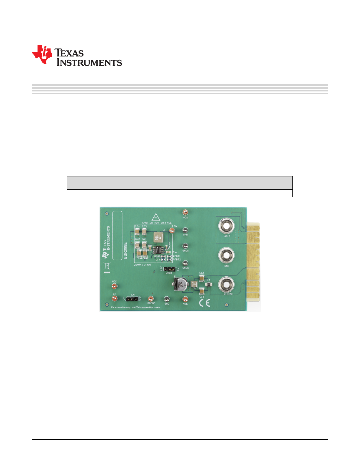
LMR36525 EVM User’s Guide
The Texas Instruments LMR36525 EVM evaluation module (EVM) helps designers evaluate the operation
and performance of the LMR36525 buck regulator. The LMR36525 is a family of easy-to-use synchronous
step-down DC/DC converters capable of driving up to 2 A of load current from an input voltage of 4.2 V to
65 V. The LMR36525 EVM features a selectable output voltage of 3.3 V or 5 V and a switching frequency
of 400 kHz. See the LMR36520 data sheet for additional features, detailed description, and available
options.
Table 1 shows the EVM options.
Table 1. Device and Package Configurations
EVM DEVICE FREQUENCY / OUTPUT
CURRENT
LMR36525AEVM LMR36525ADDAR 400 kHz / 2A No
Contents
1 Setup .......................................................................................................................... 3
2 Operation ..................................................................................................................... 5
3 Schematic..................................................................................................................... 6
4 Board Layout ................................................................................................................. 6
5 Bill of Materials............................................................................................................... 9
SPREAD
SPECTRUM
1 EVM Board Connections.................................................................................................... 3
2 EVM Card Edge Connections.............................................................................................. 3
3 Jumper Locations............................................................................................................ 4
4 FRA Setup.................................................................................................................... 5
5 LMR36525AEVM Schematic............................................................................................... 6
6 Top View of EVM ............................................................................................................ 6
7 EVM Top Copper Layer..................................................................................................... 7
SNVU677–June 2019
Submit Documentation Feedback
List of Figures
Copyright © 2019, Texas Instruments Incorporated
LMR36525 EVM User’s Guide
1
Page 2

8 EVM Mid-Layer One......................................................................................................... 7
9 EVM Mid-Layer Two......................................................................................................... 8
10 EVM Bottom Copper Layer................................................................................................. 8
1 Device and Package Configurations ...................................................................................... 1
2 BOM for LMR36525AEVM.................................................................................................. 9
Trademarks
All trademarks are the property of their respective owners.
www.ti.com
List of Tables
2
LMR36525 EVM User’s Guide
Copyright © 2019, Texas Instruments Incorporated
Submit Documentation Feedback
SNVU677–June 2019
Page 3
GND
VOUT
GNDS
VOS
TOP FRONT
BOTTOM FRONT
VIS
VINEMI
INPUT
SUPPLY
LOAD
(+) (-)
(-) (+)
(+)(-)
DMMDMM
(-)(+)
Load
(+)
(-)
Input
Supply
(-)
(+)
DMM
(-) (+)
DMM
(-) (+)
www.ti.com
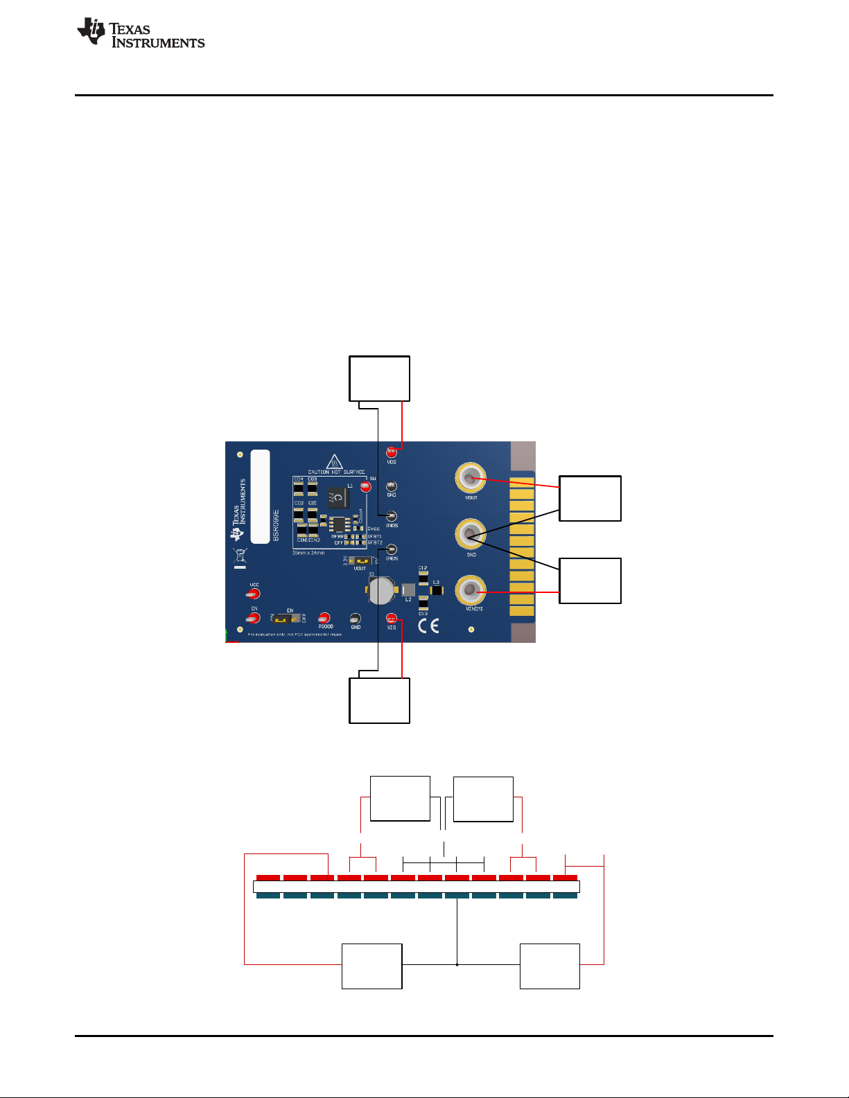
1 Setup
This section describes the test points and connectors on the EVM and how to properly connect, set up,
and use the LMR36525AEVM. Either the banana jacks and test points on the top of the board can be
used for connections, or the card edge connector can be used. See Figure 1 for the top of board
connections, and Figure 2 for the card edge connections. The following lists the functions of the
connections:
• VINEMI - Input supply to EVM with an EMI filter. Connect to a suitable input supply. See LMR36525
data sheets for input supply requirements.
• GND - System ground
• VOUT - Output of EVM. Connect to the desired load.
• VOS - Output voltage sense connection
• VIS - Input voltage sense connection
• GNDS - Ground sense point for analog measurements
Setup
SNVU677–June 2019
Submit Documentation Feedback
Figure 1. EVM Board Connections
Figure 2. EVM Card Edge Connections
3
Copyright © 2019, Texas Instruments Incorporated
LMR36525 EVM User’s Guide
Page 4

Enable
Jumper
Vout Selection
Jumper
Setup
1.1 Jumpers
See Figure 3 for jumper locations.
• EN - This jumper allows the EN input to be connected to either ground (OFF) or VIN (ON). Remove
this jumper to allow an external logic signal to control the EN function.
• VOUT - This jumper is used to select one of the two pre-defined output voltages. The "3.3 V" position
provides a 3.3 V output; while the "5 V" position provides a 5 V output.
www.ti.com
1.2 Test Points
• VINEMI - Input supply to EVM with an EMI filter. Connect to a suitable input supply. See LMR36525
data sheets for input supply requirements.
• GND - System power ground
• VOUT - Power output of EVM. Connect to the desired load.
• VOS - Output voltage sense connection; connect to DMM. Also, used for frequency response analyzer
connection.
• VIS - Input voltage sense connection; connect to DMM.
• GNDS - Ground sense point for analog measurements; connect to DMM.
• VCC - Test point to measure internal VCC of device; approximately 5 V. On-board PGOOD pullup
resistor is connected to VCC.
• EN - Connection for external EN logic input. Remove EN jumper and connect controlling logic to EN
test point for external enable control.
• PGOOD - Power-good flag output. This test point is connected to VCC through a 20 kΩ resistor. The
power good function can be monitored at this test point.
• A - Connection for frequency response analyzer (on bottom of board). See Figure 4.
Figure 3. Jumper Locations
4
LMR36525 EVM User’s Guide
Copyright © 2019, Texas Instruments Incorporated
Submit Documentation Feedback
SNVU677–June 2019
Page 5

OSC
B
A
Signal
Injection
^_/v‰µšš}
network analyzer
^_/v‰µšš}
network analyzer
www.ti.com
Operation
2 Operation
Once the above connections are made and the appropriate jumpers are set, the EVM is ready for use. If
external control of the EN input is desired, remove the EN jumper, and apply the external signal to the EN
test point and GND. The PGOOD output is pulled up to VCC through a 20-kΩ resistor. This way, the
PGOOD signal swings from 0 V to about 5 V to indicate when the output voltage is either outside or inside
of the PGOOD window, respectively. If an external pullup and supply is desired for the PGOOD function,
remove the 20-kΩ resistor, and pull the PGOOD test point up to the desired voltage through an
appropriate resistance. See the LMR36525 data sheets for more details.
The output voltage of the EVM can be selected, by the VOUT jumper, to either 3.3 V or 5 V. Other values
of output voltage can be programmed by changing the value of R
the inductor and the output capacitance may also need to be changed. See the LMR36525 data sheets for
more information.
The EVM has been designed for maximum flexibility regarding component selection. This allows you to
place preferred components, such as the inductor and capacitors, on the board and test the performance
of the regulator. This way, the power supply system can be tested before committing the design to
production.
Figure 4. FRA Setup
on the EVM. In addition, the values of
FBB
SNVU677–June 2019
Submit Documentation Feedback
Copyright © 2019, Texas Instruments Incorporated
LMR36525 EVM User’s Guide
5
Page 6

Schematic
3 Schematic
www.ti.com
4 Board Layout
Figure 5. LMR36525AEVM Schematic
Figure 6. Top View of EVM
6
LMR36525 EVM User’s Guide
Copyright © 2019, Texas Instruments Incorporated
Submit Documentation Feedback
SNVU677–June 2019
Page 7

www.ti.com
Board Layout
Figure 7. EVM Top Copper Layer
Figure 8. EVM Mid-Layer One
SNVU677–June 2019
Submit Documentation Feedback
Copyright © 2019, Texas Instruments Incorporated
LMR36525 EVM User’s Guide
7
Page 8

Board Layout
www.ti.com
Figure 9. EVM Mid-Layer Two
Figure 10. EVM Bottom Copper Layer
8
LMR36525 EVM User’s Guide
Copyright © 2019, Texas Instruments Incorporated
Submit Documentation Feedback
SNVU677–June 2019
Page 9

www.ti.com
5 Bill of Materials
DESIGNATOR COMMENT DESCRIPTION MANUFACTURER PART NUMBER QUANTITY
C1 CINB
C2, C3, C12,
C13
C4 CHF1
C5 CVcc
C6 Cboot
C7, C8, C9,
C10
C11 CFF
FID1, FID2,
FID3, FID4,
FID5, FID6
J1, J2, J3
J4, J5 EN, VOUT Header, 100 mil, 3x1, Gold, TH Samtec HTSW-103-07-G-S 2
L1
L2
L3
LBL1
R1 Rinj
R2 RFBT2 RES, 34.0 k, 1%, 0.1 W, 0603 Yageo RC0603FR-0734KL 1
R3 RFBT1 RES, 46.4 k, 1%, 0.1 W, 0603 Yageo
R4, R5 RFBB, Rpg RES, 20.0 k, 1%, 0.1 W, 0603 Yageo RC0603FR-0720KL 2
R6 RVINS
SH-J1, SH-J2 EN, VOUT
TP1, TP2, TP3,
TP4, TP5, TP6
TP7, TP8, TP9,
TP10
U1
CIN1, CIN2,
C12, C13
CO1, CO2,
CO3, CO4
GND, VOUT
XAL6060-
XAL4030-
FBMH3225H
THT-13-457-
EN, VCC,
PGOOD, SW,
VOS, VIS
GNDS, GND,
LMR36525AD
Fiducial
VINEMI,
103MEB
472MEB
M601NT
10
GNDS,
GND
DAR
Table 2. BOM for LMR36525AEVM
CAP, AL, 22 µF, 100 V, ±20%,
1.3 Ω, AEC-Q200 Grade 1,
SMD
CAP, CERM, 4.7 µF, 100 V,
±10%, X7S, AEC-Q200 Grade
1, 1210
CAP, CERM, 0.22 µF, 100 V,
±10%, X7R, 0805
CAP, CERM, 1 µF, 25 V,
±10%, X5R, 0603
CAP, CERM, 0.1 µF, 25 V,
±10%, X7R, 0603
CAP, CERM, 22 µF, 25 V,
±10%, X5R, 1210
CAP, CERM, 10 pF, 50 V,
±5%, C0G/NP0, 0603
Fiducial mark. There is nothing
to buy or mount.
Standard Banana Jack,
Uninsulated, 8.9 mm
Inductor, Shielded, Composite,
10 µH, 7 A, 0.02982 Ω, AEC-
Q200 Grade 1, SMD
Inductor, Shielded, Composite,
4.7 µH, 4.5 A, 0.0401 Ω, SMD
Ferrite Bead, 600 Ω at 100
MHz, 3 A, 1210
RES, 10.0, 1%, 0.1 W, AEC-
Q200 Grade 0, 0603
RES, 0, 5%, 0.1 W, AEC-Q200
Grade 0, 0603
Shunt, 100 mil, Gold-plated,
Black
Test Point, Multipurpose, Red,
TH
Test Point, Multipurpose,
Black, TH
SIMPLE SWITCHER(R) 4.2 V
to 65 V Synchronous Step-
Down Converter, DDA0008J
(HSOIC-8)
Bill of Materials
Panasonic EEETG2A220UP 1
TDK
MuRata
TDK
AVX 06033C104KAT2A 1
Samsung Electro-
Mechanics
MuRata
N/A N/A 0
Keystone 575-8 3
Coilcraft XAL6060-103MEB 1
Coilcraft XAL4030-472MEB 1
Taiyo Yuden
Brady THT-13-457-10 1
Vishay-Dale
Vishay-Dale
Samtec SNT-100-BK-G 2
Keystone 5010 6
Keystone 5011 4
Texas Instruments LMR36525ADDAR 1
CGA6M3X7S2A475
K200AB
GRM21AR72A224K
AC5L
C1608X5R1E105K0
80AC
CL32A226KAJNNN
E
GRM1885C1H100J
A01D
FBMH3225HM601N
T
CRCW060310R0FK
EA
RC0603FR-
0746K4L
CRCW06030000Z0
EA
4
1
1
4
0
1
1
1
1
SNVU677–June 2019
Submit Documentation Feedback
Copyright © 2019, Texas Instruments Incorporated
LMR36525 EVM User’s Guide
9
Page 10

IMPORTANT NOTICE AND DISCLAIMER
TI PROVIDES TECHNICAL AND RELIABILITY DATA (INCLUDING DATASHEETS), DESIGN RESOURCES (INCLUDING REFERENCE
DESIGNS), APPLICATION OR OTHER DESIGN ADVICE, WEB TOOLS, SAFETY INFORMATION, AND OTHER RESOURCES “AS IS”
AND WITH ALL FAULTS, AND DISCLAIMS ALL WARRANTIES, EXPRESS AND IMPLIED, INCLUDING WITHOUT LIMITATION ANY
IMPLIED WARRANTIES OF MERCHANTABILITY, FITNESS FOR A PARTICULAR PURPOSE OR NON-INFRINGEMENT OF THIRD
PARTY INTELLECTUAL PROPERTY RIGHTS.
These resources are intended for skilled developers designing with TI products. You are solely responsible for (1) selecting the appropriate
TI products for your application, (2) designing, validating and testing your application, and (3) ensuring your application meets applicable
standards, and any other safety, security, or other requirements. These resources are subject to change without notice. TI grants you
permission to use these resources only for development of an application that uses the TI products described in the resource. Other
reproduction and display of these resources is prohibited. No license is granted to any other TI intellectual property right or to any third
party intellectual property right. TI disclaims responsibility for, and you will fully indemnify TI and its representatives against, any claims,
damages, costs, losses, and liabilities arising out of your use of these resources.
TI’s products are provided subject to TI’s Terms of Sale (www.ti.com/legal/termsofsale.html) or other applicable terms available either on
ti.com or provided in conjunction with such TI products. TI’s provision of these resources does not expand or otherwise alter TI’s applicable
warranties or warranty disclaimers for TI products.
Mailing Address: Texas Instruments, Post Office Box 655303, Dallas, Texas 75265
Copyright © 2019, Texas Instruments Incorporated
 Loading...