

Page 1
User's Guide
SNVU698–March 2020
LMQ61460EVM-400K User's Guide
The LMQ61460-Q1 evaluation module (EVM) is designed to help customers evaluate the performance of
the LMQ61460-Q1 synchronous step-down voltage converter. This EVM implements the LMQ61460-Q1 in
a 14-pin wettable flanks Hotrod™ package, as shown in Table 1. It is capable of delivering 5-V output
voltage and up to 6-A load current switching at 400 kHz with exceptional efficiency and output accuracy in
a very small solution size. The EVM provides multiple power connectors and test points. In addition to an
optimized EMI board layout, the LMQ61460-Q1 uses integrated bypass capacitors which results in great
EMI performance.
Table 1. Device and Package Configurations
CONVERTER IC PACKAGE
U1 LMQ61460-Q1 14-pin wettable flanks Hotrod package 4.0 mm × 3.5 mm × 1.0 mm
SNVU698–March 2020
Submit Documentation Feedback
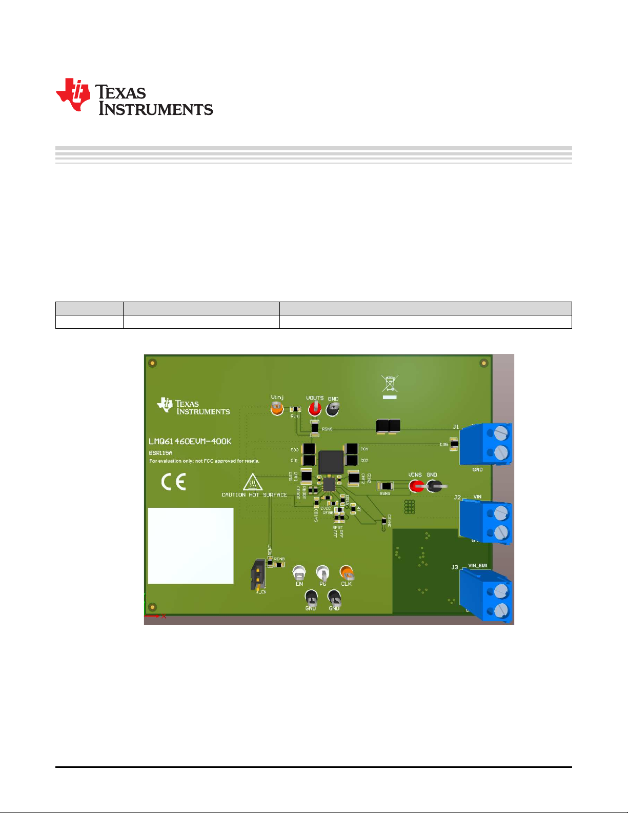
Figure 1. LMQ61460EVM-400K Top View
Copyright © 2020, Texas Instruments Incorporated
LMQ61460EVM-400K User's Guide
1
Page 2

Introduction
Contents
1 Introduction ................................................................................................................... 2
2 Quick Start Guide............................................................................................................ 3
3 Detailed Descriptions........................................................................................................ 4
4 Schematic..................................................................................................................... 5
5 Board Layout ................................................................................................................. 8
6 LMQ61460EVM-400K Board Test Results.............................................................................. 11
7 Bill of Materials ............................................................................................................. 13
Trademarks
Hotrod is a trademark of Texas Instruments.
All other trademarks are the property of their respective owners.
1 Introduction
1.1 LMQ61460-Q1 Synchronous Step-Down Voltage Converter
The LMQ61460-Q1 is an easy-to-use synchronous step-down DC/DC converter capable of delivering up
to 6 A of load current from a supply voltage ranging from 3 V to 36 V. The LMQ61460-Q1 provides
exceptional efficiency and output accuracy in a very small solution size. The LMQ61460-Q1 is capable of
delivering 6 A of load current and implements peak current mode control. The following are additional
features that provide both flexible and easy-to-use solutions for a wide range of applications:
• Adjustable switching frequency (RT)
• Synchronization to an external clock (CLK jumper)
• FPWM variant (LMQ61460AFS) (IC swap)
• Power-good flag (PG jumper)
• Precision enable (EN jumper with RENT and RENB resistors)
Automatic frequency foldback at light load and optional external bias improve efficiency over the entire
load range. The device requires few external components and has a pinout designed for optimal EMI and
thermal performance. Protection features include the following:
• Thermal shutdown
• Input undervoltage lockout
• Cycle-by-cycle current limiting
• Hiccup short-circuit protection
For a quick reference, Figure 2 shows the pin configuration of the LMQ61460-Q1.
www.ti.com
2
LMQ61460EVM-400K User's Guide
Copyright © 2020, Texas Instruments Incorporated
Submit Documentation Feedback
SNVU698–March 2020
Page 3
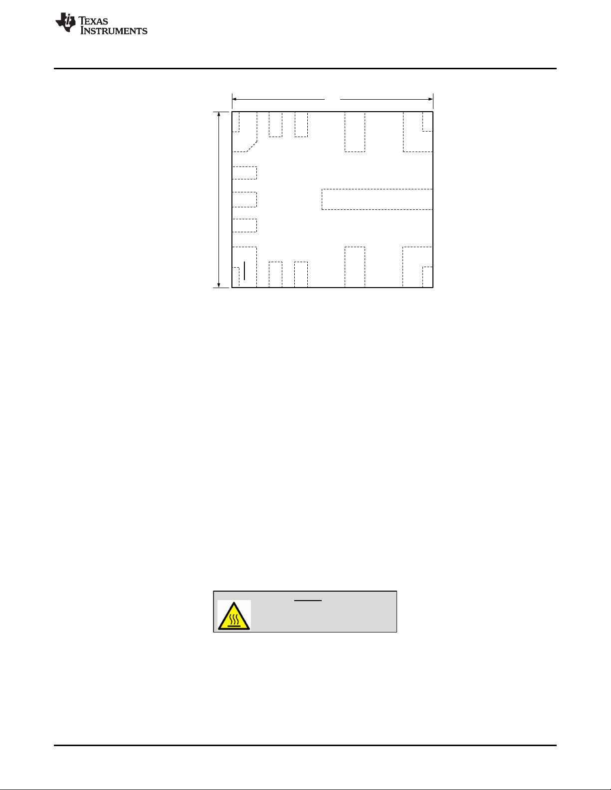
CAUTION
Caution Hot surface.
Contact may cause burns.
Do not touch.
3.5 mm
4 mm
BIAS
CBOOT
RBOOT
EN/
SYNC
RESET
VIN1
VIN2
PGND1
PGND2
SW
FB
AGND
VCC
RT
www.ti.com
Figure 2. LMQ61460-Q1 Pin Configuration (Top View)
1.2 LMQ61460-Q1 Evaluation Module
The LMQ61460EVM-400K is populated with the LMQ61460AASQRJRRQ1 which automatically reduces
frequency at light loads (PFM - pulse frequency modulation). This IC can be replaced with the
LMQ61460AFSQRJRRQ1 for a constant switching frequency across load (FPWM - forced pulse width
modulation).
Introduction
2 Quick Start Guide
1. Connect the voltage supply between the VIN and GND connectors or between VIN_EMI and
GND_EMI to include the on-board input filter in the input path. Use short and thick gauge wires to
minimize inductance and IR drop. Note that sense points for VINand V
2. Connect the load of the converter between VOUT and GND connectors using short and thick wires.
3. Set the supply voltage at an appropriate level between 6 V to 36 V. The 6 V minimum input voltage
ensures enough head room for V
supply to an appropriate level to supply needed current and protection.
4. Turn on the power supply. With the default configuration, the EVM powers up and provides V
to 5 V.
5. Monitor the output voltage with sense points. The maximum load current is 6 A with the LMQ61460Q1. Note that the maximum output current may need to derate if ambient temperature is high,
especially if device is operated at higher frequency, that is 2.2 MHz.
See Figure 4 for connector locations.
are provided.
OUT
to equal 5 V at a 6 A load current. Set the current limit of the
OUT
equal
OUT
SNVU698–March 2020
Submit Documentation Feedback
LMQ61460EVM-400K User's Guide
Copyright © 2020, Texas Instruments Incorporated
3
Page 4

Detailed Descriptions
3 Detailed Descriptions
This section describes the connectors on the EVM and how to properly connect, set up, and use the EVM.
See Figure 1 for a top view of the EVM.
VOUT —Output voltage of the converter
VOUT connectors connect to the power inductor and output capacitors. Connect the load between
the VOUT connector and the GND connector to provide load current. Connect the loading device to
the board with short and thick wires to handle the large DC output current.
GND —Ground of the converter
The GND is connected to the PGND and AGND pins of the device as well as the ground of the
input and output capacitors. The GND connections next to VIN, VIN_EMI, and VOUT connectors
are meant for current return path for the supply voltage and load, respectively. Connectors are
provided in pairs to allow easy and accurate sensing of voltages. Connect to supply and load
grounds with short and thick wires. Other GND connectors are for signal measurement and probing.
VIN— Input voltage to the converter
The VINconnector connects to the input capacitors and the VIN pins of the LMQ61460-Q1. Connect
the supply voltage from a power supply or a battery between VIN and GND connectors as power
input to the device. The input voltage (VIN) range must be higher than 3.9 V for the device to start
up and above 3 V to maintain operation. A VINhigher than 6 V provides a regulated 5-V output
voltage. Maximum VINis limited to 36 V to avoid damaging the device. The current limit on the
supply must be high enough to provide the needed supply current. The supply voltage must be
connected to the board with short and thick wires to handle the required input current at maximum
load current. If long cables are used to power up the board, damping must be provided by adding
CFLT3 and RFLT3 to avoid oscillation between the cable parasitic inductance and the existing lowESR ceramic capacitors.
www.ti.com
VIN_EMI —Low EMI option
If the input filter is required, connect the supply voltage between VIN_EMI and GND_EMI. The
supply voltage must be connected to the board with short and thick wires.
The input filter consists of the following: CF1, CF2, CF3, CF4, CF5, CF6, and L2. CD1, CD2, RD1,
and RD2 are provided to allow more options for filter optimization. To include the input filter in the
power path, connect the supply voltage between the VIN_EMI and GND_EMI connectors. The
output of the filter is connected to VIN, which is connected to the VINpins of the LMQ61460-Q1.
Conducted EMI arises from the operation of switching circuits.
GND_EMI —Ground return for the input filter
This is the current return path for the supply connected to VIN_EMI. It provides a short-loop
connection to the input filter capacitors to best filter the conducted noise generated from the PCB.
Use VIN_EMI and GND_EMI connection if input filter is used and conducted EMI test is desired.
CLK —For synchronization clock input
The CLK input connector is designed for external clock input to the EN/SYNC pin. Switching action
of the buck is synchronized to the external clock when it is present. The operation mode
automatically changes to forced PWM mode, maintaining a constant switching frequency over the
entire load range while the clock signal is present.
EN — To monitor the EN pin or control EN signal
This test point is used to monitor the voltage on the device EN pin. By default, the EN pin is
connected to the mid-point of an enable divider. Note that the lower resistor in this divider, RENB, is
not populated so the IC turns on by default. Populate RENB to adjust UVLO. Apply a voltage to EN
to externally enable or disable the device.
PG — To monitor the PGOOD/RESET pin
The PGOOD flag indicates whether the output voltage is within the regulation band. The RESET
pin (synonymous with PGOOD pin) of the device is an open-drain output and is pulled up to V
OUT
through a 100 k resistor. This pin pulls to GND when the output voltage is out of regulation.
4
LMQ61460EVM-400K User's Guide
Copyright © 2020, Texas Instruments Incorporated
Submit Documentation Feedback
SNVU698–March 2020
Page 5

www.ti.com
Vinj —For measuring AC response
A low value resistor, Rinj, is placed between VOUT and this node. The feedback divider of the
board is connected to this node. An AC signal is applied across Rinj when taking measurements for
bode plots.
VOUTS —VOUT sense
This connector is provided for measuring the output voltage accurately.
VINS —VIN sense
This connector is provided for measuring the input voltage accurately.
4 Schematic
The bill of materials is tabulated in Section 7. In addition, Figure 3 shows the corresponding schematic.
Schematic
SNVU698–March 2020
Submit Documentation Feedback
Copyright © 2020, Texas Instruments Incorporated
LMQ61460EVM-400K User's Guide
5
Page 6
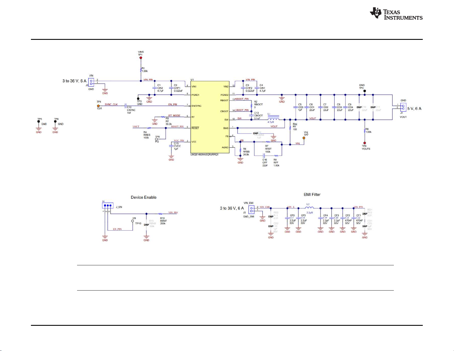
Schematic
www.ti.com
NOTE: Long leads and additional inductance in used to power the DC/DC may cause issues for ideal device operation. RD2, CD2, RD1, and
CD1 are placeholders for damping networks to be populated. For more information regarding this topic, reference the EMI Filter
Components and Their Nonidealities for Automotive DC/DC Regulators Technical Brief.
6
LMQ61460EVM-400K User's Guide
Figure 3. LMQ61460EVM-400K Schematic
SNVU698–March 2020
Submit Documentation Feedback
Copyright © 2020, Texas Instruments Incorporated
Page 7

www.ti.com
4.1 Alternative BOM Configurations
VOUT FREQUENCY RFBB RT COUT CIN + CHF L1
3.3 V 400 kHz 43.2 kΩ 33.2 kΩ 6 x 22 µF 2 x 4.7 µF + 2 x
3.3 V 2100 kHz 43.2 kΩ 6.04 kΩ 3 x 22 µF 2 x 4.7 µF + 2 x
5 V 400 kHz 24.9 kΩ 33.2 kΩ 4 x 22 µF 2 x 4.7 µF + 2 x
5 V 2100 kHz 24.9 kΩ 6.04 kΩ 3 x 22 µF 2 x 4.7 µF + 2 x
Table 2. BOM Configurations
100 nF
100 nF
100 nF
100 nF
Schematic
4.7 µH
(XHMI6060)
1 µH (XEL5030)
4.7 µH
(XHMI6060)
1 µH (XEL5030)
SNVU698–March 2020
Submit Documentation Feedback
Copyright © 2020, Texas Instruments Incorporated
LMQ61460EVM-400K User's Guide
7
Page 8

Board Layout
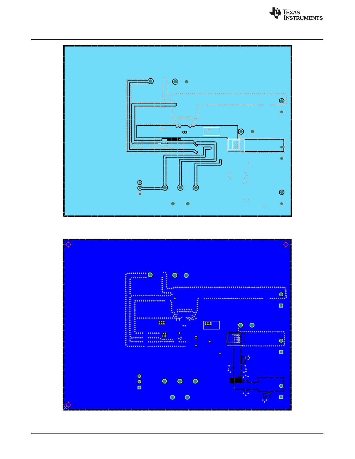
5 Board Layout
Figure 4 through Figure 8 show the board layout for the LMQ61460-Q1 EVM. The EVM offers resistors,
capacitors, and test points to configure the following:
• Output voltage (RFBT and RFBB)
• Precision enable pin (RENT and RENB)
• Set frequency (RT)
• External clock synchronization (CLK jumper)
The 14-pin Hotrod package with integrated capacitors offers a very small size and low-noise solution. The
PCB consists of a 4-layer design. There are 2-oz copper planes on the top and bottom and 1-oz copper
mid-layer planes to route signals and dissipate heat with an array of thermal vias to connect to all four
layers.
Test points have been provided for ease of use to connect the power supply and required load, and to
monitor critical signals.
The board measures 3.00" x 4.00" (76mm x 101mm).
www.ti.com
Figure 4. Top View with Silkscreen
8
LMQ61460EVM-400K User's Guide
Copyright © 2020, Texas Instruments Incorporated
Submit Documentation Feedback
SNVU698–March 2020
Page 9

www.ti.com
Board Layout
Figure 5. Top Layer
SNVU698–March 2020
Submit Documentation Feedback
Figure 6. Signal Layer 1 - Ground Plane
Copyright © 2020, Texas Instruments Incorporated
LMQ61460EVM-400K User's Guide
9
Page 10
Board Layout
www.ti.com
Figure 7. Signal Layer 2 - Routing
10
LMQ61460EVM-400K User's Guide
Figure 8. Bottom Layer
Copyright © 2020, Texas Instruments Incorporated
Submit Documentation Feedback
SNVU698–March 2020
Page 11

www.ti.com
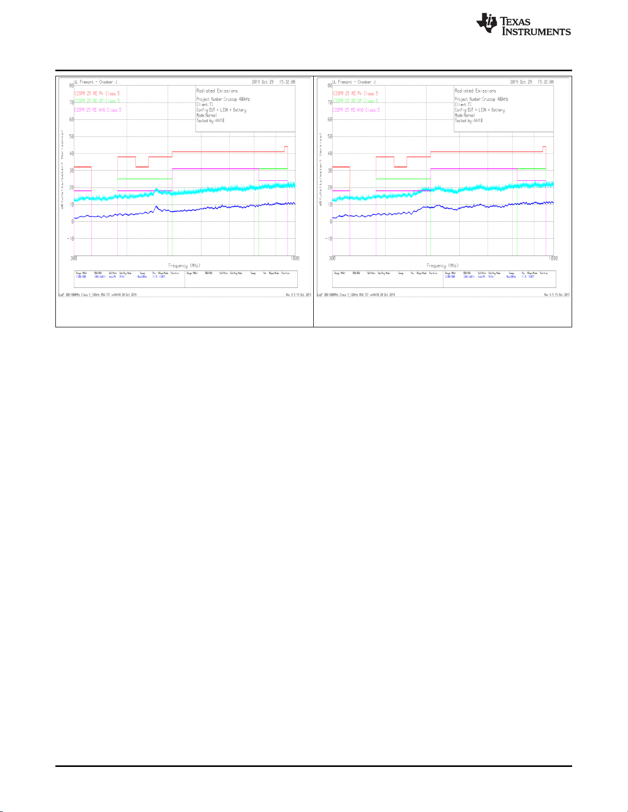
6 LMQ61460EVM-400K Board Test Results
6.1 EMI
The EMI measurements were taken following CISPR 25, Class 5 standards. The measurements were
taken at 13.5 VIN, 5 VOUT with a 6 A load switching at 400kHz.
LMQ61460EVM-400K Board Test Results
Figure 9. Conducted EMI Measurement with CISPR 25
Class 5 Limit Lines (150 kHz to 30 MHz)
Figure 11. Radiated EMI Measurement with Horizontal
Bicon Antenna Under CISPR 25 Class 5 Limits
Figure 10. Conducted EMI Measurement with CISPR 25
Class 5 Limit Lines (30 MHz to 108 MHz)
Figure 12. Radiated EMI Measurement with Vertical Bicon
Antenna Under CISPR 25 Class 5 Limits
SNVU698–March 2020
Submit Documentation Feedback
Copyright © 2020, Texas Instruments Incorporated
LMQ61460EVM-400K User's Guide
11
Page 12
LMQ61460EVM-400K Board Test Results
www.ti.com
Figure 13. Radiated EMI Measurement with Horizontal Log
Antenna Under CISPR 25 Class 5 Limits
Figure 14. Radiated EMI Measurement with Vertical Log
Antenna Under CISPR 25 Class 5 Limits
12
LMQ61460EVM-400K User's Guide
Copyright © 2020, Texas Instruments Incorporated
Submit Documentation Feedback
SNVU698–March 2020
Page 13
www.ti.com
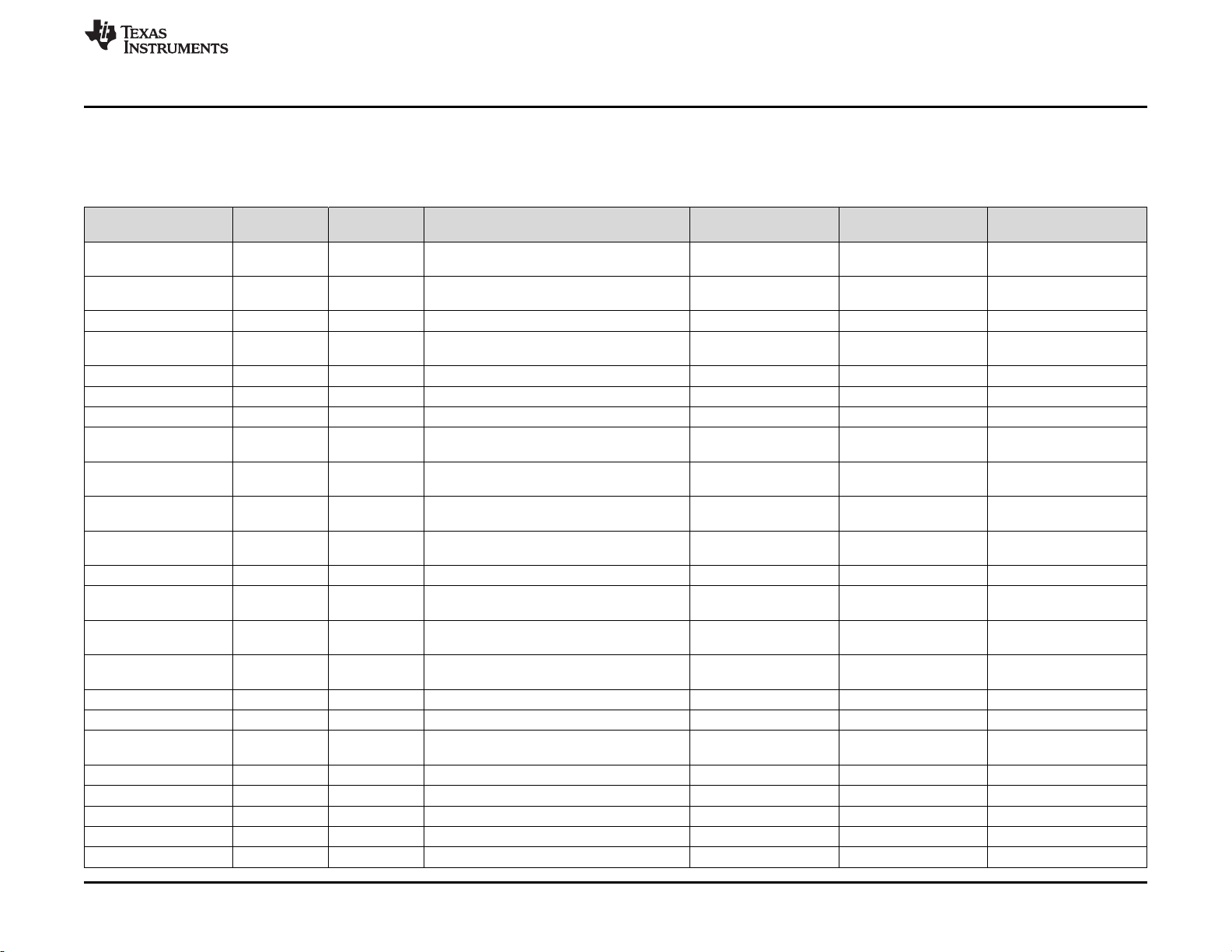
7 Bill of Materials
The bill of materials is shown Table 3 for the LMQ61460EVM-400K.
Bill of Materials
Table 3. LMQ61460EVM-400K EVM Bill of Materials
DESIGNATOR QUANTITY VALUE DESCRIPTION
C1, C4 2 4.7 µF CAP, CERM, 4.7 µF, 50 V, ±20%, X7R, AEC-
Q200 Grade 1, 1210
C2, C3 2 0.022 µF CAP, CERM, 0.022 µF, 50 V, ±10%, X7R,
0402
C5 1 1 µF CAP, CERM, 1 µF, 25 V, ±10%, X7R, 0805 0805 C0805C105K3RACTU Kemet
C6, C7, C8, C9 4 22 µF CAP, CERM, 22 µF, 16 V, ±20%, X7R, AEC-
Q200 Grade 1, 1210
C12 1 1000 pF CAP, CERM, 1000 pF, 50 V, ±0%, X7R, 0603 0603 C0603C102K5RACTU Kemet
C13 1 0.1 µF CAP, CERM, 0.1 µF, 10 V, ±10%, X7R, 0603 0603 C0603X104K8RACTU Kemet
C15 1 1 µF CAP, CERM, 1 µF, 16 V, ±10%, X7R, 0603 0603 885012206052 Wurth Elektronik
C16 1 22 pF CAP, CERM, 22 pF, 50 V, ±5%, C0G/NP0,
AEC-Q200 Grade 1, 0603
C17, C18, C19, C20 4 2.2 µF CAP, CERM, 2.2 µF, 50 V, ±10%, X7R, AEC-
Q200 Grade 1, 0805
C21, C22 2 0.47 µF CAP, CERM, 0.47 µF, 50 V, ±10%, X7R,
AEC-Q200 Grade 1, 0603
J1, J2, J3 3 Terminal Block, 5 mm, 2x1, Tin, TH Terminal Block, 5 mm,
J4 1 Header, 100 mil, 3x1, Gold, TH Header, 100 mil, 3x1, TH HTSW-103-07-G-S Samtec
L1 1 4.7 µH Inductor, Shielded, Hyperflux, 4.7 µH, 7.4 A,
0.0143 Ω , SMD
L2 1 1.2 µH Shielded Molded Inductor 7.5 A, 11.3
mΩ Max 2-SMD
LBL1 1 PCB Label 0.650 x 0.200
R1, R6 2 1.00 k RES, 1.00 k, 1%, 0.25 W, 1206 1206 RC1206FR-071KL Yageo America
R2 1 0 RES, 0, 5%, 0.1 W, 0603 0603 RC0603JR-070RL Yageo
R3 1 33.2 k RES, 33.2 k, 1%, 0.1 W, AEC-Q200 Grade 0,
0603
R4, R7 2 100 k RES, 100 k, 1%, 0.1 W, 0603 0603 RC0603FR-07100KL Yageo
R5 1 100 RES, 100, 1%, 0.1 W, 0603 0603 RC0603FR-07100RL Yageo
R8 1 24.9 k RES, 24.9 k, 1%, 0.1 W, 0603 0603 RC0603FR-0724K9L Yageo
R9 1 1.00 k RES, 1.00 k, 1%, 0.1 W, 0603 0603 ERJ-3EKF1001V Panasonic
R10 1 255 k RES, 255 k, 1%, 0.1 W, 0603 0603 RC0603FR-07255KL Yageo
PACKAGE
REFERENCE
1210 UMK325B7475MMHT Taiyo Yuden
0402 GRM155R71H223KA12DMuRata
1210 CGA6P1X7R1C226M25
0603 CGA3E2C0G1H220J080AATDK
0805 CGA4J3X7R1H225K125ABTDK
0603 CGA3E3X7R1H474K080AETDK
2x1, TH
6.65x6.45 mm 74439346047 Wurth Elektronik
SMD2 744316220 Wurth Electronics
inch
0603 CRCW060333K2FKEA Vishay-Dale
PART NUMBER MANUFACTURER
TDK
0AC
691 101 710 002 Wurth Elektronik
THT-14-423-10 Brady
SNVU698–March 2020
Submit Documentation Feedback
Copyright © 2020, Texas Instruments Incorporated
LMQ61460EVM-400K User's Guide
13
Page 14

Bill of Materials
Table 3. LMQ61460EVM-400K EVM Bill of Materials (continued)
DESIGNATOR QUANTITY VALUE DESCRIPTION
SH-J1 1 Shunt, 100 mil, Gold plated, Black Shunt 2 pos. 100 mil 881545-2 TE Connectivity
TP1, TP9 2 Test Point, Multipurpose, Red, TH Red Multipurpose
TP2, TP3, TP5, TP6 4 Test Point, Multipurpose, Black, TH Black Multipurpose
TP4, TP7 2 Test Point, Multipurpose, Orange, TH Orange Multipurpose
TP8, TP10 2 Test Point, Multipurpose, White, TH White Multipurpose
U1 1 Automotive 6-A Low Noise Synchronous Buck
C10, C11 0 22 µF CAP, CERM, 22 µF, 16 V, ±20%, X7R, AEC-
C14 0 1 µF CAP, CERM, 1 µF, 10 V, ±10%, X7R, 0603 0603 GRM188R71A105KA61DMuRata
C23, C24 0 1 µF CAP, CERM, 1 µF, 50 V, ±10%, X7R, 0603 0603 UMK107AB7105KA-T Taiyo Yuden
FID1, FID2, FID3, FID4,
FID5, FID6
R12 0 0.51 RES, 0.51, 1%, 0.25 W, 0805 0805 CRM0805-FX-R510ELF Bourns
R13 0 100 k RES, 100 k, 1%, 0.1 W, 0603 0603 RC0603FR-07100KL Yageo
0 Fiducial mark. There is nothing to buy or
Regulators, RJR0014A (VQFN-HR-14)
Q200 Grade 1, 1210
mount.
PACKAGE
REFERENCE
Testpoint
Testpoint
Testpoint
Testpoint
RJR0014A LMQ61460AASQRJRRQ1Texas Instruments
1210 CGA6P1X7R1C226M25
N/A N/A N/A
PART NUMBER MANUFACTURER
5010 Keystone
5011 Keystone
5013 Keystone
5012 Keystone
TDK
0AC
www.ti.com
14
LMQ61460EVM-400K User's Guide
Submit Documentation Feedback
SNVU698–March 2020
Copyright © 2020, Texas Instruments Incorporated
Page 15

IMPORTANT NOTICE AND DISCLAIMER
TI PROVIDES TECHNICAL AND RELIABILITY DATA (INCLUDING DATASHEETS), DESIGN RESOURCES (INCLUDING REFERENCE
DESIGNS), APPLICATION OR OTHER DESIGN ADVICE, WEB TOOLS, SAFETY INFORMATION, AND OTHER RESOURCES “AS IS”
AND WITH ALL FAULTS, AND DISCLAIMS ALL WARRANTIES, EXPRESS AND IMPLIED, INCLUDING WITHOUT LIMITATION ANY
IMPLIED WARRANTIES OF MERCHANTABILITY, FITNESS FOR A PARTICULAR PURPOSE OR NON-INFRINGEMENT OF THIRD
PARTY INTELLECTUAL PROPERTY RIGHTS.
These resources are intended for skilled developers designing with TI products. You are solely responsible for (1) selecting the appropriate
TI products for your application, (2) designing, validating and testing your application, and (3) ensuring your application meets applicable
standards, and any other safety, security, or other requirements. These resources are subject to change without notice. TI grants you
permission to use these resources only for development of an application that uses the TI products described in the resource. Other
reproduction and display of these resources is prohibited. No license is granted to any other TI intellectual property right or to any third
party intellectual property right. TI disclaims responsibility for, and you will fully indemnify TI and its representatives against, any claims,
damages, costs, losses, and liabilities arising out of your use of these resources.
TI’s products are provided subject to TI’s Terms of Sale (www.ti.com/legal/termsofsale.html) or other applicable terms available either on
ti.com or provided in conjunction with such TI products. TI’s provision of these resources does not expand or otherwise alter TI’s applicable
warranties or warranty disclaimers for TI products.
Mailing Address: Texas Instruments, Post Office Box 655303, Dallas, Texas 75265
Copyright © 2020, Texas Instruments Incorporated
 Loading...