

Page 1

Table of Contents
LMP91050 Evaluation Board
User’s Guide for the LMP91050 Evaluation Board with Sensor
AFE Software
1.0. Introduction ........................................................................................................................................ 1
2.0. Equipment .......................................................................................................................................... 2
2.1. Connection Diagram .......................................................................................................................... 2
2.2. Board Assembly ................................................................................................................................. 3
3.0. Quick Start ......................................................................................................................................... 4
4.0. Powering the LMP91050SDEVAL .................................................................................................... 11
5.0. Evaluating the LMP91050 without the SPIO-4 Board. ..................................................................... 11
6.0. Installing the LMP91050 Sensor AFE Software ................................................................................ 12
7.0. Schematic ........................................................................................................................................... 13
8.0. Layout ................................................................................................................................................ 14
9.0. BOM .................................................................................................................................................. 15
1.0. Introduction
The LMP91050 Design Kit (consisting of the LMP91050 Evaluation Board, the SPIO-4 Digital
Controller Board, the Sensor AFE software, and this user’s guide) is designed to ease evaluation and
design-in of Texas Instrument’s LMP91050 Configurable AFE for Nondispersive In frared (NDIR).
Data capturing and evaluations are simplified by connecting the SPIO-4 Digital Controller Board (SPIO-4
board) to a PC via USB and running the Sensor AFE software. The data capture board will generate the
SPI signals to communicate to and capture data from the LMP91050. The user will also have the option
to evaluate the LMP91050 without using the SPIO-4 board or the Sensor AFE software.
The on board data converter will digitize the LMP91050’s analog output, and the software will display
these results in time domain and histogram. The software also allows customers to write to and read from
registers, to configure the device’s gain, output offset, and common mode voltage, and most importantly,
to configure and learn about the LMP91050.
This document describes the connection between the boards and PC, and provides a quick start for
voltage measurements. This document also describes how to evaluate the LMP91050 with and without
the SPIO-4 board and provides the schematic, board layout, and BOM.
© 2011 Texas Instrum e nts Incorporated Page 1 of 17 lmp91050sdeval_usersguide_v7.doc
Page 2
2.0. Equipment
1. LMP91050 evaluation board (NSID: LMP91050SDEVAL)
2. SPIO-4 digital controller board (NSID: SPIO-4)
3. Power supplies (optional) to source VDD-EXT or IN_DUT.
4. Multimeter
5. PC with Sensor AFE software
6. NDIR Thermopile Sensor (optional)
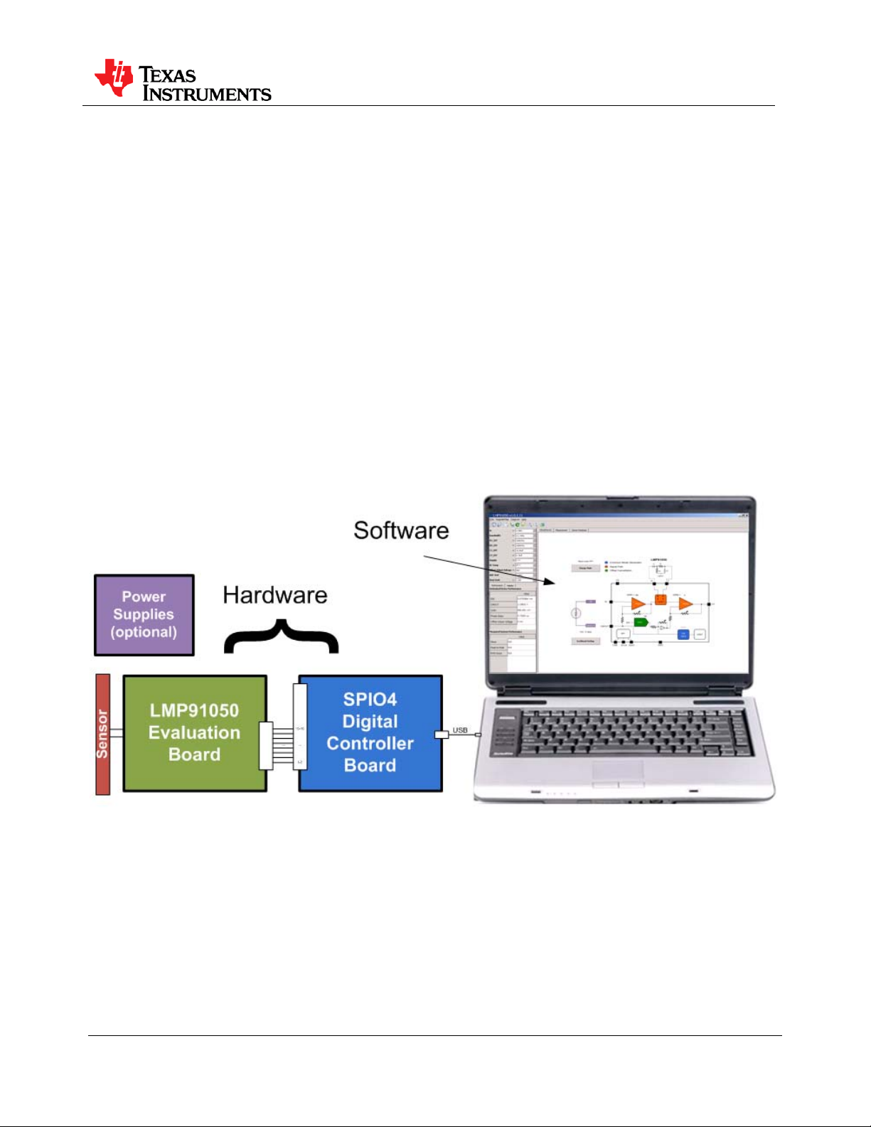
2.1. Connection Diagram
Figure 1 shows the connection between the LMP91050 Evaluation Board (LMP91050SDEVAL),
SPIO-4 board, and a personal computer with the LMP91050 Sensor AFE software. LMP91050 can
be powered using external power supplies or from the SPIO-4 board.
LMP91050 Evaluation Board
Figure 1 – Connection Diagram
© 2011 Texas Instrum e nts Incorporated Page 2 of 17 lmp91050sdeval_usersguide_v7.doc
Page 3
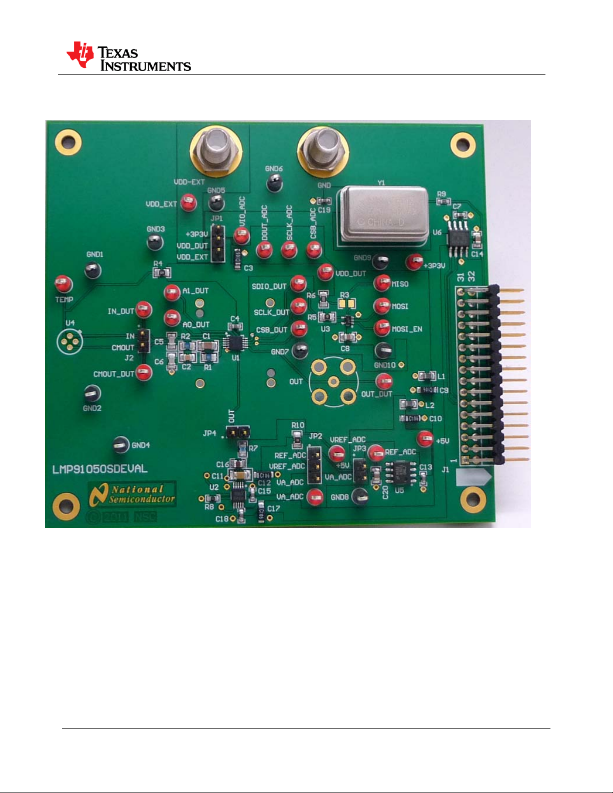
2.2. Board Assembly
LMP91050 Evaluation Board
Figure 2 – LMP91050 Evaluation Board Assembly
© 2011 Texas Instrum e nts Incorporated Page 3 of 17 lmp91050sdeval_usersguide_v7.doc
Page 4
LMP91050 Evaluation Board
3.0. Quick Start
The following procedures show a quick method to assemble the LMP91050SDEVAL and perform a quick
voltage reading.
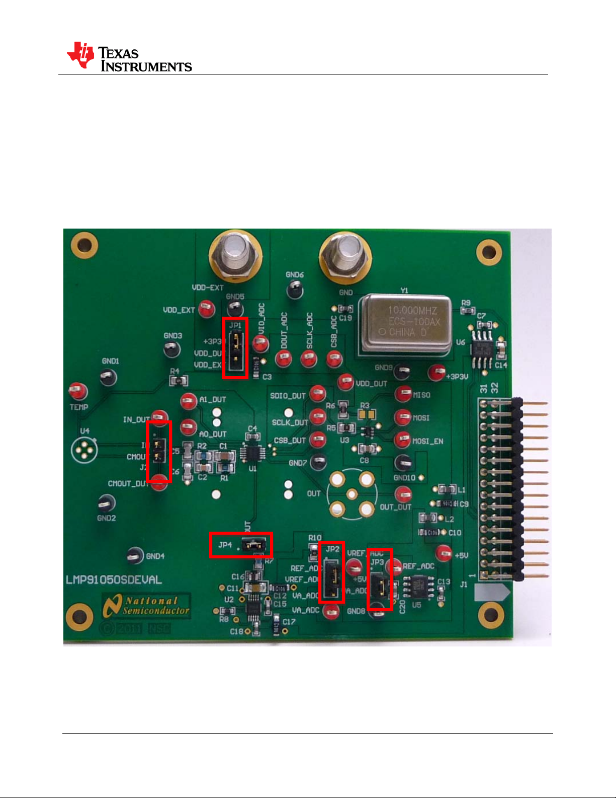
A. LMP91050 EVB Jumper Connections
1. The jumpers for this example application can be seen in Figure 3 and Table 1
2. The SPIO-4 board is properly setup out of the box (no assembly required).
3. The schematic for the LMP91050SDEVAL can be seen in Figure 10.
Figure 3 – Jumper Settings (Default) for voltage reading
© 2011 Texas Instrum e nts Incorporated Page 4 of 17 lmp91050sdeval_usersguide_v7.doc
Page 5
Jumpers
Pin
Purpose
JP1: VDD_DUT
P1-P2
Connect LMP91050 VDD to +3.3V from SPIO4
JP2: VREF_ADC
P1-P2
Connect ADC VREF to 4.1V from U5 (LM4140)
JP3: VA_ADC
P1-P2
Connect ADC VA to +5V from SPIO4
JP4: OUT_DUT to
ADC
P1-P2
Connect LMP91050 OUT to ADC input RC filter
J2: IN to CMOUT
Open
Connect LMP91050 IN to CMOUT. Note: Bo ard is
short IN to CMOUT for easy evaluation.
provided with this jumper open. Use provided jumper to
Table 1 - Jumpers for Voltage Measurement
B. Installing/Opening the Software - follow section 6.0 to install and open the LMP91050 Sensor
AFE software.
C. Connecting and Powering the Boards – these steps have to be done in this order.
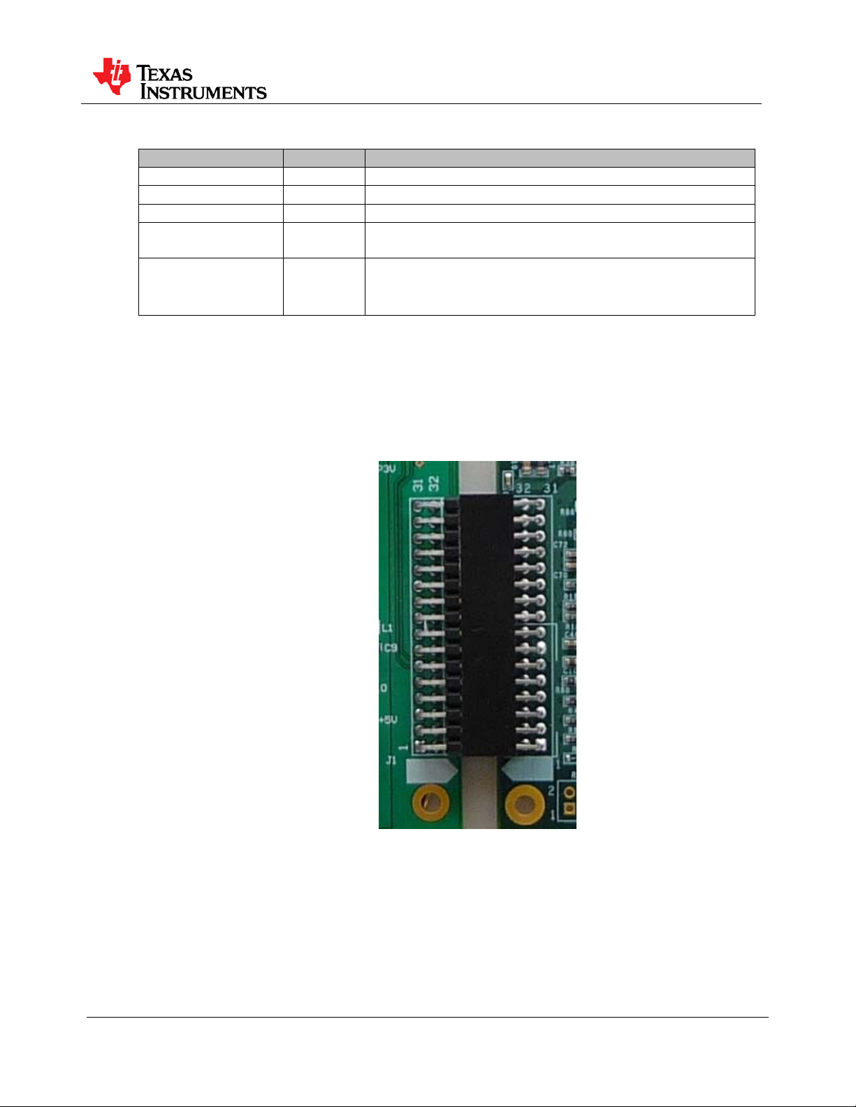
1. Connect the LMP91050SDEVAL’s J1 to SPIO-4 Board’s J6. See Figure 4.
LMP91050 Evaluation Board
Figure 4 – LMP91050SDEVAL-to-SPIO-4 Board Connection
2. Connect SPIO-4 board to a PC via USB.
3. Use a multimeter to measure LMP91050SDEVAL’s +5V test point; it should be
approximately 5V. If it is not, check your power supplies and jumpers. Measure test point
VREF_ADC; it should be approximately 4.1V. If it’s not, check your jumpers and U5.
© 2011 Texas Instrum e nts Incorporated Page 5 of 17 lmp91050sdeval_usersguide_v7.doc
Page 6
1 2 3 4 5
LMP91050 Evaluation Board
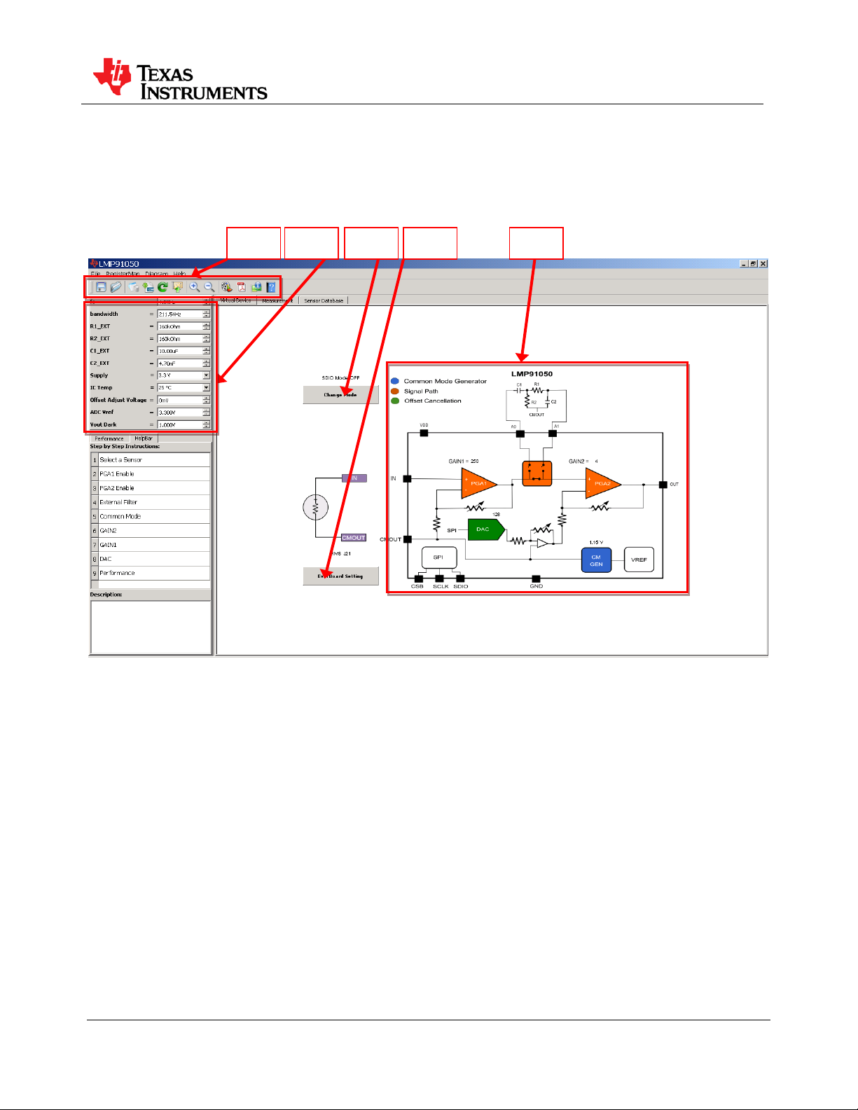
D. Sensor AFE Software Overview
Once connection between the boards and PC is established, you can use the software to com m unicate to and
capture data from the LMP91050. Drag cursor over window icons to get an icon description. Some items of
interest are shown in Figure 5.
Figure 5 – Sensor AFE Items of Interest
1. Menu Bar Icons (from left to right)
a. Save Configuration to File: Saves the current configuration settings (register
settings) to an .xml file.
b. Load Configuration File: Loads the selected configuration settings (register
settings) .xml file.
c. Register Map: Opens Register Map window. An alternative to the Virtual
Device, for writing and reading the device registers. See datasheet for details on
device Register Map.
d. Save All Registers to File: Saves register contents to a .cvs file.
e. Read All Register from Board: After configuring the register map, use this button
to read all registers. Functional only in SDIO Mode (see Item 3).
f. Write All Registers To Board: After configuring the register map use this button
to write all registers. Registers will not be updated until this step is done.
g. Zoo m In/Out Diagram Ima g e: Zoom in and out of the virtual device image.
h. Show Tutorial: Takes you to the interactive Software Overview videos.
i. Documentation: Accesses the LMP91050 Datasheet, SPIO4 User’s Guide, or
Evaluation Board User’s Guide.
2. User Inputs
© 2011 Texas Instrum e nts Incorporated Page 6 of 17 lmp91050sdeval_usersguide_v7.doc
Page 7

a. fc: Center frequency of external bandpass filter.
b. bandwidth: Pass band bandwidth of external bandpass filter.
c. R1_EXT, R2_EXT, C1_EXT, C2_EXT: External bandpass filter component
values calculated based on user input for center frequency (fc) and pass band
(bandwidth) described above.
d. Supply: LMP91050 supply voltage (VDD).
e. IC Temp: LMP91050 operating temperature
f. Offset Adjust Voltage: The tool will calculate the DAC code (decimal) required
to achieve this output offset adjust voltage. User must then Write to the register
to update the value in the NDAC register.
g. ADC Vref: ADC reference voltage. User should inpu t v alue m easured at
VREF_ADC test point. Value used to calculate displayed Output Voltage.
h. Vout Dark: This value corresponds to the user measured value at the LMP91050
output (OUT) when input is shorted (IN = CMOUT). Tool will use this value to
estimate LMP91050 input voltage (IN - CMOUT) on subsequent measurements.
3. Change Mode: Change between device Read Mode OFF (default) and ON. See datasheet
for details on SPI Read Mode.
4. Eval Board Setting: Document to show user how to configure jumpers and connect
thermopile based on sensor selected.
5. Virtual Device: Drag cursor across color coded blocks and click to configure each block.
To update registers “Write A ll Regis ters ” when done.
E. Configuring the LMP91050 Using the Sensor AFE Software
Follow the step-by-step instructions under the “HelpBar” mini-tab (left hand side of the GUI) to
configure the LMP91050 for this example. These step-by-step instructions are discussed in
details below, and the recommended configuration should look similar to Figure 6.
LMP91050 Evaluation Board
© 2011 Texas Instrum e nts Incorporated Page 7 of 17 lmp91050sdeval_usersguide_v7.doc
Page 8

LMP91050 Evaluation Board
Figure 6 - Recommended LMP91050 Conf ig uration for a voltage Reading
1. Step 1: Select a Sensor – Sensor Database window opens. See Figure 7. Step 1: Click sensor
type (Thermopile) and the sensors will show in the bottom table. Step 2: Click sensor and
then click “Select” button on the left to use this sensor.
© 2011 Texas Instrum e nts Incorporated Page 8 of 17 lmp91050sdeval_usersguide_v7.doc
Page 9

Step 1
Step 2
LMP91050 Evaluation Board
Figure 7 – Sensor Database Window
2. Step 2: PGA1 Enable – click on the “PGA1” block to set “1: PGA1 ON” . Remember after
configuring the register map to use the Write All Registers button to update the registers.
3. Step 3: PGA2 Enable – click on the “PGA2” block to set “1: PGA2 ON” . Note: By default
PGA1 and PGA2 are OFF on power up. However the software was designed to automatically
power ON PGA1 and PGA2 for ease of use.
4. Step 4: External Filter – click on the switch block to choose “0: PGA1 to PGA2 direct”
(default).
5. Step 5: Common Mode – click on the “CM GEN” block to set “0: 1.15V” (default).
6. Step 6: GAIN 2 – click on the “PGA2” block to set “00: 4” (default).
7. Step 7: GAIN 1 – click on the “PGA1” block to set “0: 250” (default).
8. Step 8: DAC (Output Offset) – click on the “DAC” block to set “128” (default) for 0 mV
offset. Alternatively, user can also use the Offset Adjust Voltage user input field to input 0
mV.
9. Step 9: Performance - click on the “Performance” mini-tab. This tab displays the Estimated
Device Performance based on device configuration and user input device Supply and IC
Temp .This tab also displays the Measured System Performance if you’ve connected a board
and ran the LMP91050.
© 2011 Texas Instrum e nts Incorporated Page 9 of 17 lmp91050sdeval_usersguide_v7.doc
Page 10

F. Capturing Data
1. Click on the “Measurement” tab.
2. Under the “Output Format” field, select Display as “Output Voltage (V)”
3. Under the “Stop Condition” field, select Run as “1” Seconds. Alternatively, select “Run
Continuously” radio button to run continuously up to 1 hour.
4. Click on the “Run” button to view the output voltage results. A reading should be plotted as
seen in Figure 8 . Output voltage will vary depending on input voltage across IN_DUT and
CMOUT_DUT. If J2 is shorted, IN_DUT = CMOUT_DUT, output voltage should be about
1V. Note: Board is provided with jumper J2 open. Use provided jumper to short IN to
CMOUT for easy evaluation.
LMP91050 Evaluation Board
Figure 8 - Results for DC Reading
© 2011 Texas Instrum e nts Incorporated Page 10 of 17 lmp91050sdeval_usersguide_v7.doc
Page 11

LMP91050 Evaluation Board
4.0. Powering the LMP91050SDEVAL
There are two ways in which VDD can be sourced: external supply or SPIO-4 power.
If using an external power supply to source VDD, do the following:
1. Connect an external power supply to banan a jack s VDD-EXT and GND.
2. Jumper pins 2 and 3 of JP1 to connect the external power to VDD_DUT.
If using the SPIO-4 power to source VDD, then do the following:
1. Jumper pins 1 and 2 of JP1 to connect +3.3V SPIO-4 power to VDD_DUT.
The schematic for the LMP91050SDEVAL can be seen in Figure 10.
5.0. Evaluating the LMP91050 without the SPIO-4 Board.
The SPIO-4 digital controller board is used to generate the SPI signals to communicate to the
LMP91050. Without the SPIO-4 board, the Sensor AFE software for the LMP91050 cannot be used
to capture and analyze data from the LMP91050SDEVAL.
If the SPIO-4 board is not available but LMP91050 evaluation is desirable, then connect your own
SPI signals to J1 of the LMP91050SDEVAL as seen below. Reference the LMP91050 datasheet for
appropriate SPI timing diagrams. Source LMP91050 VDD with an external power supply per
previous section.
Figure 9 - LMP91050SDEVAL’s J1 for SPI Signals
Refer to the LMP91050 datasheet for more information on the LMP91050’s SPI protocol.
© 2011 Texas Instrum e nts Incorporated Page 11 of 17 lmp91050sdeval_usersguide_v7.doc
Page 12

LMP91050 Evaluation Board
6.0. Installing the LMP91050 Sensor AFE Software
Each Sensor AFE product will have its own software. To access the Sensor AFE software for
LMP91050, follow the steps below.
1. Getting the Zip Files
a. You can find the latest downloadable Sensor AFE software at
ti.com/sensorafe
b. Download the zip file onto your local hard drive. Unzip this folder.
2. Installing the Driver - skip this step if you don’t have the LMP91050SDEVAL and SPIO4
digital controller board.
a. See the provided Installat ion Guide For SensorAFE Drivers.pdf.
3. Installing the Software
a. See the provided Installation Guide for LMP91050 SensorAFE Software.pdf
i. Note: If you run the software without the boards, you’ll get an error message. Ignore
that error message and click “Ok” to continue.
© 2011 Texas Instrum e nts Incorporated Page 12 of 17 lmp91050sdeval_usersguide_v7.doc
Page 13

Note 1) Thermopile sensor U4 is not included.
7.0. Schematic
LMP91050 Evaluation Board
© 2011 Texas Instrum e nts Incorporated Page 13 of 17 lmp91050sdeval_usersguide_v7.doc
Figure 10 - LMP91050SDEVAL Schematic
Page 14

8.0. Layout
LMP91050 Evaluation Board
Figure 11 - Layout
© 2011 Texas Instrum e nts Incorporated Page 14 of 17 lmp91050sdeval_usersguide_v7.doc
Page 15

Item
Designator
Description
Manufacturer
PartNumber
Quantity
1
+3P3V, +5V, A0_DUT, A1_DUT, CMOUT_DUT, CS B_ADC,
Test Point, TH, Compact, Red
Keystone
5005
23
2
AA1
Printed Circuit Board
N/A
PCB
1
4
C2
CAP CER 4700PF 250V X7R 10%
TDK
C2012X7R2E472K
1
5
C3, C9, C10, C12, C17
CAP, TANT, 10uF, 10V, +/-20%,
3.4 ohm, 3216-18 SMD
Vishay-
Sprague
293D106X0010A2TE3
5
6
C4, C7, C13, C15, C18, C19
CAP, CERM, 0.1uF, 16V, +/-5%,
X7R, 0603
AVX
0603YC104JAT2A
6
7
C5, C6
CAP, CERM, 10nF, 50V, +/-5%,
C0G/NP0, 0805
MuRata
GRM2195C1H103JA01D
2
8
C8, C14
CAP, CERM, 0.1uF, 25V, +/-10%,
X7R, 0805
AVX
08053C104KAT2A
2
9
C11
CAP, CERM, 0.1uF, 100V, +/-5%,
X7R, 1206
AVX
12061C104JAT2A
1
10
C16, C20
CAP, CERM, 1uF, 10V, +/-10%,
X7R, 0805
AVX
0805ZC105KAT2A
2
DNS (Connector, TH, BNC)
Connex
Uninsulated, 15A
Components
13
GND1, GND2, GND3, GND4, GND5, GND6, GND7, GND8, GND9,
Test Point, TH, Compact, Black
Keystone
5006
10
14
N/A
BUMPON HEMISPHERE .44X.20
4
15
J1
SPIO-GPSI32 Header, 72-Pin, Dual
Sullins
PBC36DGAN
1
16
J2, JP3, JP4
Header, TH, 100mil, 2x1, Gold
Samtec Inc.
TSW-102-07-G-S
3
17
JP1, JP2
Header, TH, 100mil, 1x3, Gold
Samtec Inc.
TSW-103-07-G-S
2
18
L1, L2
Ferrite, Chip, 200mA, .80 ohm,
Wurth
BLM21BD272SN1L
2
9.0. BOM
LMP91050 Evaluation Board
CSB_DUT, DOUT_ADC, IN_DUT, MISO, MOSI, MOSI_EN,
OUT_DUT, REF_ADC, SCLK_ADC, SCLK_DUT , SDI_DUT,
TEMP, VA_ADC, VDD_DUT, VDD_EXT, VI O _ADC, VREF_ADC
3 C1 CAP CER 10UF 16V X7R 10%
1206
0805
11 OUT
12 GND, VDD-EXT Standard Banana Jack,
GND10
BLACK 3M SJ-5003 (BLACK)
Electronics
TDK C3216X7R1C106K 1
Amphenol
Johnson
Electronics
112404 1
108-0740-001 2
© 2011 Texas Instrum e nts Incorporated Page 15 of 17 lmp91050sdeval_usersguide_v7.doc
row, Right Angle
plated, 230 mil above insulator
plated, 230 mil above insulator
SMD
Connector
Solutions
Elektronik
eiSos
Page 16

20
R3
DNS (RES, 0 ohm, 5%, 0.125W,
0805)
Vishay-Dale
CRCW08050000Z0EA
0
21
R5, R10
RES, 0 ohm, 5%, 0.125W, 0805
Vishay-Dale
CRCW08050000Z0EA
2
22
R4
RES, 100k ohm, 5%, 0.125W, 0805
Vishay-Dale
CRCW0805100KJNEA
1
23
R6
RES, 100k ohm, 1%, 0.125W, 0805
Vishay-Dale
CRCW0805100KFKEA
1
24
R7
RES, 1.00k ohm, 1%, 0.125W,
Vishay-Dale
CRCW08051K00FKEA
1
25
R8
RES, 27.4 ohm, 1%, 0.1W, 0603
Vishay-Dale
CRCW060327R4FKEA
1
27
U1
DNS (Configurable AFE for NDIR)
Texas
Instruments
LMP91050
1
28
U2
14-Bit, 200 kSPS, Pseudo10-pin Mini SOIC, Pb-Free
Texas
ADC141S628QIMMX/NO
1
29
U3
Non-Inverting 3-State Buffer
On
Semiconductor
MC74VHC1G125DFT1
1
30
U4
DNS (Thermopile Sensor)
0
31
U6
2K 5.0V I2C Serial EEPROM
Microchip
24C02C/SN
1
32
Y1
Osc 10.000Mhz 5.0V Full Size
ECS Inc
ECS-100AX-100
1
SOIC
LMP91050 Evaluation Board
19 R1, R2 RES, 160k ohm, 5%, 0.125W, 0805 Vishay-Dale CRCW0805160KJNEA 2
0805
26 R9 RES, 51.1 ohm, 1%, 0.1W, 0603 Vishay-Dale CRCW060351R1FKEA 1
Differential Input, MicroPower ADC,
33 U5 Precision Micropower Low Dropout
Voltage Reference, 8-pin Narrow
34 Oscillator Socket Aries
Instruments
Instruments
Electronics
Table 2 - BOM
Texas
PB
LM4140ACM-4.1/NOPB 1
1107741 1
© 2011 Texas Instrum e nts Incorporated Page 16 of 17 lmp91050sdeval_usersguide_v7.doc
Page 17

LMP91050 Evaluation Board
Evaluation Board/Kit Important Noti ce
Texas Instruments (TI) provides the enclosed product(s) under the following conditions:
This evaluation board/kit is intended for use for ENGINEERING DEVELOPMENT, DEM ONSTRATION, OR EVALUATION
PURPOSES ONL Y and is not considered by TI to be a finished end-product fit for general consumer use. Pers ons handli ng the
product(s) must have electronics training and observe good engineering practice standards. As such, the goods being provided are
not intended to be complete in terms of required design-, marketing-, and/or manufacturing-related protective considerations,
including product safety and environmental measures typically found in end products that incorporate such semiconductor
components or circuit boards. This evaluation board/kit does not fall within the scope of the European Union directives regarding
electromagnetic compatibility, restricted substances (RoHS), recycl i ng (WEEE), FCC, CE or UL, and therefore may not meet the
technical requirements of these directives or other related directives.
Should this evaluation board/kit not meet the specifications indicated in the User’s Guide, the board/kit may be returned within 30
days from the date of delivery for a full refund. THE FOREGOING WARRANTY IS THE EXCLUSIVE WARRANTY MADE BY
SELLER TO BUYER AND IS IN LIEU OF ALL OTHER WARRANTIES, EXPRESSED, IMPLIED, OR STATUTORY, INCLUDING
ANY WARRANTY OF MERCHANTABILITY OR FITNESS F OR ANY PARTI CULAR PURPOSE.
The user assumes all responsibility and liability for proper and safe handling of the goods. Further, the user indemnifies TI from all
claims arising from the handling or use of the goods. Due to the open construction of the product, it is the user’s responsibility to
take any and all appropriate precautions with regard to electrostatic discharge.
EXCEPT TO THE EXTENT OF THE INDEMNITY SET FORTH ABOVE, NEITHER PARTY SHALL BE LIABLE TO THE OTHER
FOR ANY INDIRECT, SPECIAL, INCIDENTA L, O R CONSEQUE NTIAL DAMAGES.
TI currently deals with a variety of customers for products, and therefore our arrangement with the user is not exclusive.
TI assumes no liability for applications assistance, customer product design, software performance, or infringement of
patents or services described herein.
Please read the User’s Guide and, specifically, the Warnings and Restrictions notice in the User’s Guide prior to handling the
product. This notice contains important safety information about temperatures and voltages. For additional inf orm ation on TI’s
environmental and/or safety programs, please contact the TI application engineer or visit www.ti.com/esh.
No license is granted under any patent right or other intellectual property right of TI covering or relating to any machine, process, or
combination in which such TI products or services might be or are used.
FCC Warning
This evaluation board/kit is intended for use for ENGINEERING DEVELOPMENT, DEM ONSTRATION, OR EVALUATION
PURPOSES ONL Y and is not considered by TI to be a finished end-product fit for general consumer use. It generates, uses, and
can radiate radio frequency energy and has not been tested for compliance with the limits of computing devices pursuant to part 15
of FCC rules, which are designed to provide reasonable protection against radio frequency interference. Operat i on of this
equipment in other environments may cause interference with radio communications, in which case the user at his own expense
will be required to take whatever measures may be required to correct this interference.
EVM Warnings and Restrictions
It is important to operate this EVM within the input voltage range of 3.3V to 5V and the output voltage range of 0V to 5V.
Exceeding the specified input range may cause unexpected operation and/or irreversible damage to the EVM. If there are
questions concerning the input range, please contact a TI field representative prior to connecting the input power.
Applying loads outside of the specified output range may result in unintended operation and/or possible permanent damage to the
EVM. Please consult the EVM User's Guide prior to connecting any load to the EVM output. If there is uncertainty as to the load
specification, please contact a TI field representative.
During normal operation, some circuit components may have case temperatures greater than +30°C. The EVM is designed to
operate properly with certain components above +85°C as long as the input and output ranges are maintained. These components
include but are not limited to linear regulators, switching transistors, pass transistors, and current sense resistors. These types of
devices can be identified using the EVM schematic located in the EVM User's Guide. When placing measurement probes near
these devices during operation, please be aware that these devices may be very warm to the touch.
Mailing Address: Texas Instruments, Post Office Box 655303, Dallas, Texas 75265
Copyright © 2011, Texas Instruments Incorporated
© 2011 Texas Instrum e nts Incorporated Page 17 of 17 lmp91050sdeval_usersguide_v7.doc
Page 18

IMPORTANT NOTICE
Texas Instruments Incorporated and its subsidiaries (TI) reserve the right to make corrections, modifications, enhancements, improvements,
and other changes to its products and services at any time and to discontinue any product or service without notice. Customers should
obtain the latest relevant information before placing orders and should verify that such information is current and complete. All products are
sold subject to TI’s terms and conditions of sale supplied at the time of order acknowledgment.
TI warrants performance of its hardware products to the specifications applicable at the time of sale in accordance with TI’s standard
warranty. Testing and other quality control techniques are used to the extent TI deems necessary to support this warranty. Except where
mandated by government requirements, testing of all parameters of each product is not necessarily performed.
TI assumes no liability for applications assistance or customer product design. Customers are responsible for their products and
applications using TI components. To minimize the risks associated with customer products and applications, customers should provide
adequate design and operating safeguards.
TI does not warrant or represent that any license, either express or implied, is granted under any TI patent right, copyright, mask work right,
or other TI intellectual property right relating to any combination, machine, or process in which TI products or services are used. Information
published by TI regarding third-party products or services does not constitute a license from TI to use such products or services or a
warranty or endorsement thereof. Use of such information may require a license from a third party under the patents or other intellectual
property of the third party, or a license from TI under the patents or other intellectual property of TI.
Reproduction of TI information in TI data books or data sheets is permissible only if reproduction is without alteration and is accompanied
by all associated warranties, conditions, limitations, and notices. Reproduction of this information with alteration is an unfair and deceptive
business practice. TI is not responsible or liable for such altered documentation. Information of third parties may be subject to additional
restrictions.
Resale of TI products or services with statements different from or beyond the parameters stated by TI for that product or service voids all
express and any implied warranties for the associated TI product or service and is an unfair and deceptive business practice. TI is not
responsible or liable for any such statements.
TI products are not authorized for use in safety-critical applications (such as life support) where a failure of the TI product would reasonably
be expected to cause severe personal injury or death, unless officers of the parties have executed an agreement specifically governing
such use. Buyers represent that they have all necessary expertise in the safety and regulatory ramifications of their applications, and
acknowledge and agree that they are solely responsible for all legal, regulatory and safety-related requirements concerning their products
and any use of TI products in such safety-critical applications, notwithstanding any applications-related information or support that may be
provided by TI. Further, Buyers must fully indemnify TI and its representatives against any damages arising out of the use of TI products in
such safety-critical applications.
TI products are neither designed nor intended for use in military/aerospace applications or environments unless the TI products are
specifically designated by TI as military-grade or "enhanced plastic." Only products designated by TI as military-grade meet military
specifications. Buyers acknowledge and agree that any such use of TI products which TI has not designated as military-grade is solely at
the Buyer's risk, and that they are solely responsible for compliance with all legal and regulatory requirements in connection with such use.
TI products are neither designed nor intended for use in automotive applications or environments unless the specific TI products are
designated by TI as compliant with ISO/TS 16949 requirements. Buyers acknowledge and agree that, if they use any non-designated
products in automotive applications, TI will not be responsible for any failure to meet such requirements.
Following are URLs where you can obtain information on other Texas Instruments products and application solutions:
Products Applications
Audio www.ti.com/audio Automotive and Transportation www.ti.com/automotive
Amplifiers amplifier.ti.com Communications and Telecom www.ti.com/communications
Data Converters dataconverter.ti.com Computers and Peripherals www.ti.com/computers
DLP® Products www.dlp.com Consumer Electronics www.ti.com/consumer-apps
DSP dsp.ti.com Energy and Lighting www.ti.com/energy
Clocks and Timers www.ti.com/clocks Industrial www.ti.com/industrial
Interface interface.ti.com Medical www.ti.com/medical
Logic logic.ti.com Security www.ti.com/security
Power Mgmt power.ti.com Space, Avionics and Defense www.ti.com/space-avionics-defense
Microcontrollers microcontroller.ti.com Video and Imaging www.ti.com/video
RFID www.ti-rfid.com
OMAP Mobile Processors www.ti.com/omap
Wireless Connectivity www.ti.com/wirelessconnectivity
TI E2E Community Home Page e2e.ti.com
Mailing Address: Texas Instruments, Post Office Box 655303, Dallas, Texas 75265
Copyright © 2012, Texas Instruments Incorporated
 Loading...