

Page 1

LMP7731
LMP7731 2.9 nV/sqrt(Hz) Low Noise, Precision, RRIO Amplifier
Literature Number: SNOSAT6D
Page 2

LMP7731
May 20, 2009
2.9 nV/sqrt(Hz) Low Noise, Precision, RRIO Amplifier
General Description
The LMP7731 is a single, low noise, rail-to-rail input and output, low voltage amplifier. The LMP7731 is part of the LMP
®
precision amplifier family and is ideal for precision and low
noise applications with low voltage requirements.
This operational amplifier offers low voltage noise of 2.9 nV/
√Hz with a 1/f corner of only 3 Hz. The LMP7731 has bipolar
input stages with a bias current of only 1.5 nA. This low input
bias current, complemented by the very low level of voltage
noise, makes the LMP7731 an excellent choice for photometry applications.
The LMP7731 provides a wide GBW of 22 MHz while consuming only 2 mA of current. This high gain bandwidth along
with the high open loop gain of 130 dB enables accurate signal conditioning in applications with high closed loop gain
requirements.
The LMP7731 has a supply voltage range of 1.8V to 5.5V,
making it an ideal choice for battery operated portable applications.
The LMP7731 is offered in the space saving 5-Pin SOT-23
and 8-Pin SOIC packages.
Features
(Typical values, TA = 25°C, VS = 5V)
■
Input voltage noise
—
f = 3 Hz 3.3 nV/√Hz
—
f = 1 kHz 2.9 nV/√Hz
■
CMRR 130 dB
■
Open loop gain 130 dB
■
GBW 22 MHz
■
Slew rate 2.4 V/µs
■
THD @ f = 10 kHz, AV = +1, RL = 2 kΩ 0.001%
■
Supply current per channel 2.2 mA
■
Supply voltage range 1.8V to 5.5V
■
Operating temperature range −40°C to 125°C
■
Input bias current ±1.5 nA
■
RRIO
Applications
■
Gas analysis instruments
■
Photometric instrumentation
■
Medical instrumentation
Typical Performance Characteristics
Input Voltage Noise vs. Frequency
20175261
Input Current Noise vs. Frequency
20175262
LMP® is a registered trademark of National Semiconductor Corporation.
© 2009 National Semiconductor Corporation 201752 www.national.com
LMP7731 2.9 nV/sqrt(Hz) Low Noise, Precision, RRIO Amplifier
Page 3
Absolute Maximum Ratings (Note 1)
If Military/Aerospace specified devices are required,
please contact the National Semiconductor Sales Office/
Distributors for availability and specifications.
ESD Tolerance (Note 2)
Human Body Model
Inputs pins only 2000V
All other pins 2000V
Machine Model 200V
Charge Device Model 1000V
VIN Differential
±2V
Supply Voltage (VS = V+ – V−)
6.0V
Storage Temperature Range −65°C to 150°C
Junction Temperature (Note 3) +150°C max
Soldering Information
Infrared or Convection (20 sec) 235°C
Wave Soldering Lead Temp. (10 sec) 260°C
Operating Ratings (Note 1)
Temperature Range −40°C to 125°C
Supply Voltage (VS = V+ – V–)
1.8V to 5.5V
Package Thermal Resistance (θJA)
5-Pin SOT-23 265°C/W
8-Pin SOIC 190°C/W
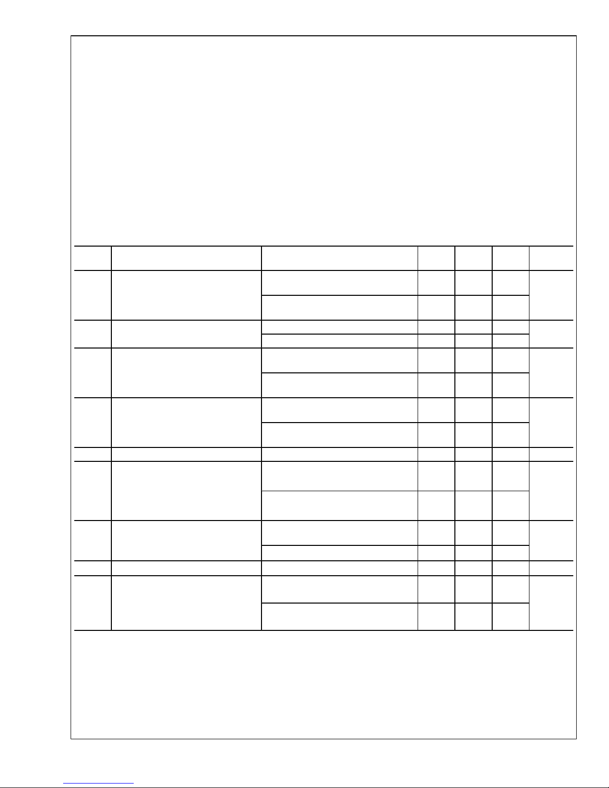
2.5V Electrical Characteristics (Note 4)
Unless otherwise specified, all limits are guaranteed for TA = 25°C, V+ = 2.5V, V− = 0V, VCM = V+/2, RL >10 kΩ to V+/2. Boldface limits apply at the temperature extremes.
Symbol Parameter Conditions
Min
(Note 6)
Typ
(Note 5)
Max
(Note 6)
Units
V
OS
Input Offset Voltage
(Note 7)
VCM = 2.0V
±9
±500
±600
μV
VCM = 0.5V
±9
±500
±600
TCV
OS
Input Offset Voltage Temperature Drift
VCM = 2.0V ±0.5 ±5.5
μV/°C
VCM = 0.5V ±0.2 ±5.5
I
B
Input Bias Current
VCM = 2.0V
±1
±30
±45
nA
VCM = 0.5V
±12
±50
±75
I
OS
Input Offset Current
VCM = 2.0V
±1
±50
±75
nA
VCM = 0.5V
±11
±60
±80
TCI
OS
Input Offset Current Drift VCM = 0.5V and VCM = 2.0V 0.0474 nA/°C
CMRR Common Mode Rejection Ratio
0.15V ≤ VCM ≤ 0.7V
0.23V ≤ VCM ≤ 0.7V
101
89
120
dB
1.5V ≤ VCM ≤ 2.35V
1.5V ≤ VCM ≤ 2.27V
105
99
129
PSRR Power Supply Rejection Ratio
2.5V ≤ V+ ≤ 5V
111
105
129
dB
1.8V ≤ V+ ≤ 5.5V
117
CMVR Common Mode Voltage Range
Large Signal CMRR ≥ 80 dB
0 2.5
V
A
VOL
Open Loop Voltage Gain
RL = 10 kΩ to V+/2
V
OUT
= 0.5V to 2.0V
112
104
130
dB
RL = 2 kΩ to V+/2
V
OUT
= 0.5V to 2.0V
109
90
119
www.national.com 2
LMP7731
Page 4
Symbol Parameter Conditions
Min
(Note 6)
Typ
(Note 5)
Max
(Note 6)
Units
V
OUT
Output Voltage Swing High
RL = 10 kΩ to V+/2
4
50
75
mV from
either rail
RL = 2 kΩ to V+/2
13
50
75
Output Voltage Swing Low
RL = 10 kΩ to V+/2
6
50
75
RL = 2 kΩ to V+/2
9
50
75
I
OUT
Output Current
Sourcing, V
OUT
= V+/2
VIN (diff) = 100 mV
22
12
31
mA
Sinking, V
OUT
= V+/2
VIN (diff) = −100 mV
15
10
44
I
S
Supply Current
(Per Channel)
VCM = 2.0V
2.0 2.7
3.4
mA
VCM = 0.5V
2.3 3.1
3.9
SR Slew Rate
AV = +1, CL = 10 pF, RL = 10 kΩ to V+/2,
VO = 2 V
PP
2.4
V/μs
GBW Gain Bandwidth
CL = 20 pF, RL = 10 kΩ to V+/2
21 MHz
G
M
Gain Margin
CL = 20 pF, RL = 10 kΩ to V+/2
14 dB
Φ
M
Phase Margin
CL = 20 pF, RL = 10 kΩ to V+/2
60 deg
R
IN
Input Resistance
Differential Mode 38
kΩ
Common Mode 151
MΩ
THD+N Total Harmonic Distortion + Noise AV = 1, f = 1 kHz, Amplitude = 1V 0.002 %
e
n
Input Referred Voltage Noise Density
f = 1 kHz, VCM = 2.0V 3
nV/
f = 1 kHz, VCM = 0.5V 3
Input Voltage Noise 0.1 Hz to 10 Hz 75 nV
PP
i
n
Input Referred Current Noise Density
f = 1 kHz, VCM = 2.0V 1.1
pA/
f = 1 kHz, VCM = 0.5V 2.3
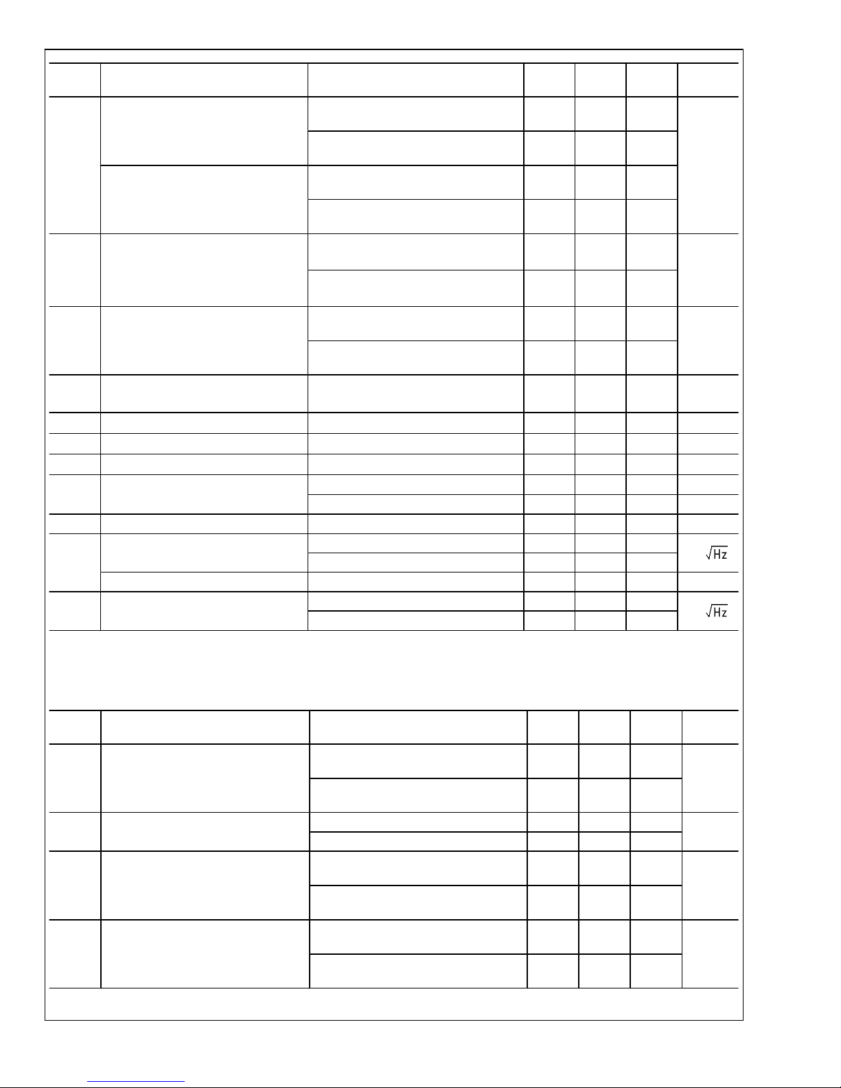
3.3V Electrical Characteristics (Note 4)
Unless otherwise specified, all limits are guaranteed for TA = 25°C, V+ = 3.3V, V− = 0V, VCM = V+/2, RL > 10 kΩ to V+/2. Boldface limits apply at the temperature extremes.
Symbol Parameter Conditions
Min
(Note 6)
Typ
(Note 5)
Max
(Note 6)
Units
V
OS
Input Offset Voltage
(Note 7)
VCM = 2.5V
±6
±500
±600
μV
VCM = 0.5V
±6
±500
±600
TCV
OS
Input Offset Voltage Temperature Drift
VCM = 2.5V ±0.5 ±5.5
μV/°C
VCM = 0.5V ±0.2 ±5.5
I
B
Input Bias Current
VCM = 2.5V
±1.5
±30
±45
nA
VCM = 0.5V
±13
±50
±77
I
OS
Input Offset Current
VCM = 2.5V
±1
±50
±70
nA
VCM = 0.5V
±11
±60
±80
3 www.national.com
LMP7731
Page 5

Symbol Parameter Conditions
Min
(Note 6)
Typ
(Note 5)
Max
(Note 6)
Units
TCI
OS
Input Offset Current Drift VCM = 0.5V and VCM = 2.5V
0.048 nA/°C
CMRR Common Mode Rejection Ratio
0.15V ≤ VCM ≤ 0.7V
0.23V ≤ VCM ≤ 0.7V
101
89
120
dB
1.5V ≤ VCM ≤ 3.15V
1.5V ≤ VCM ≤ 3.07V
105
99
130
PSRR Power Supply Rejection Ratio
2.5V ≤ V+ ≤ 5.0V
111
105
129
dB
1.8V ≤ V+ ≤ 5.5V
117
CMVR Common Mode Voltage Range
Large Signal CMRR ≥ 80 dB
0 3.3
V
A
VOL
Open Loop Voltage Gain
RL = 10 kΩ to V+/2
V
OUT
= 0.5V to 2.8V
112
104
130
dB
RL = 2 kΩ to V+/2
V
OUT
= 0.5V to 2.8V
110
92
119
V
OUT
Output Voltage Swing High
RL = 10 kΩ to V+/2
5
50
75
mV from
either rail
RL = 2 kΩ to V+/2
14
50
75
Output Voltage Swing Low
RL = 10 kΩ to V+/2
9
50
75
RL = 2 kΩ to V+/2
13
50
75
I
OUT
Output Current
Sourcing, V
OUT
= V+/2
VIN (diff) = 100 mV
28
22
45
mA
Sinking, V
OUT
= V+/2
VIN (diff) = -100 mV
25
20
48
I
S
Supply Current
(Per Channel)
VCM = 2.5V
2.1
2.8
3.5
mA
VCM = 0.5V
2.4
3.2
4.0
SR Slew Rate
AV = +1, CL = 10 pF, RL = 10 kΩ to V+/2,
V
OUT
= 2 V
PP
2.4
V/μs
GBW Gain Bandwidth
CL = 20 pF, RL = 10 kΩ to V+/2
22 MHz
G
M
Gain Margin
CL = 20 pF, RL = 10 kΩ to V+/2
14 dB
Φ
M
Phase Margin
CL = 20 pF, RL = 10 kΩ to V+/2
62 deg
R
IN
Input Resistance
Differential Mode 38
kΩ
Common Mode 151
MΩ
THD+N Total Harmonic Distortion + Noise AV = 1, f = 1 kHz, Amplitude = 1V, 0.002 %
e
n
Input Referred Voltage Noise Density
f = 1 kHz, VCM = 2.5V 2.9
nV/
f = 1 kHz, VCM = 0.5V 2.9
Input Voltage Noise 0.1 Hz to 10 Hz 65 nV
PP
i
n
Input Referred Current Noise Density
f = 1 kHz, VCM = 2.5V 1.1
pA/
f = 1 kHz, VCM = 0.5V 2.1
www.national.com 4
LMP7731
Page 6

5V Electrical Characteristics (Note 4)
Unless otherwise specified, all limits are guaranteed for TA = 25°C, V+ = 5V, V− = 0V, VCM = V+/2, RL > 10 kΩ to V+/2. Boldface
limits apply at the temperature extremes.
Symbol Parameter Conditions
Min
(Note 6)
Typ
(Note 5)
Max
(Note 6)
Units
V
OS
Input Offset Voltage
(Note 7)
VCM = 4.5V
±6
±500
±600
μV
VCM = 0.5V
±6
±500
±600
TCV
OS
Input Offset Voltage Temperature Drift
VCM = 4.5V ±0.5 ±5.5
μV/°C
VCM = 0.5V ±0.2 ±5.5
I
B
Input Bias Current
VCM = 4.5V
±1.5
±30
±50
nA
VCM = 0.5V
±14
±50
±85
I
OS
Input Offset Current
VCM = 4.5V
±1
±50
±70
nA
VCM = 0.5V
±11
±65
±80
TCI
OS
Input Offset Current Drift VCM = 0.5V and VCM = 4.5V 0.0482 nA/°C
CMRR Common Mode Rejection Ratio
0.15V ≤ VCM ≤ 0.7V
0.23V ≤ VCM ≤ 0.7V
101
89
120
dB
1.5V ≤ VCM ≤ 4.85V
1.5V ≤ VCM ≤ 4.77V
105
99
130
PSRR Power Supply Rejection Ratio
2.5V ≤ V+ ≤ 5V
111
105
129
dB
1.8V ≤ V+ ≤ 5.5V
117
CMVR Common Mode Voltage Range
Large Signal CMRR ≥ 80 dB
0 5
V
A
VOL
Open Loop Voltage Gain
RL = 10 kΩ to V+/2
V
OUT
= 0.5V to 4.5V
112
104
130
dB
RL = 2 kΩ to V+/2
V
OUT
= 0.5V to 4.5V
110
94
119
V
OUT
Output Voltage Swing High
RL = 10 kΩ to V+/2
8
50
75
mV from
either rail
RL = 2 kΩ to V+/2
24
50
75
Output Voltage Swing Low
RL = 10 kΩ to V+/2
9
50
75
RL = 2 kΩ to V+/2
23
50
75
I
OUT
Output Current
Sourcing, V
OUT
= V+/2
VIN (diff) = 100 mV
33
27
47
mA
Sinking, V
OUT
= V+/2
VIN (diff) = -100 mV
30
25
49
I
S
Supply Current
(Per Channel)
VCM = 4.5V
2.2
3.0
3.7
mA
VCM = 0.5V
2.5
3.4
4.2
SR Slew Rate
AV = +1, CL = 10 pF, RL = 10 kΩ to V+/2,
V
OUT
= 2 V
PP
2.4
V/μs
GBW Gain Bandwidth
CL = 20 pF, RL = 10 kΩ to V+/2
22 MHz
5 www.national.com
LMP7731
Page 7

Symbol Parameter Conditions
Min
(Note 6)
Typ
(Note 5)
Max
(Note 6)
Units
G
M
Gain Margin
CL = 20 pF, RL = 10 kΩ to V+/2
12 dB
Φ
M
Phase Margin
CL = 20 pF, RL = 10 kΩ to V+/2
65 deg
R
IN
Input Resistance
Differential Mode 38
kΩ
Common Mode 151
MΩ
THD+N Total Harmonic Distortion + Noise AV = 1, f = 1 kHz, Amplitude = 1V 0.001 %
e
n
Input Referred Voltage Noise Density
f = 1 kHz, VCM = 4.5V 2.9
nV/
f = 1 kHz, VCM = 0.5V 2.9
Input Voltage Noise 0.1 Hz to 10 Hz 78 nV
PP
i
n
Input Referred Current Noise Density
f = 1 kHz, VCM = 4.5V 1.1
pA/
f = 1 kHz, VCM = 0.5V 2.2
Note 1: Absolute Maximum Ratings indicate limits beyond which damage to the device may occur. Operating Ratings indicate conditions for which the device is
intended to be functional, but specific performance is not guaranteed. For guaranteed specifications and the test conditions, see the Electrical Characteristics
Tables.
Note 2: Human Body Model, applicable std. MIL-STD-883, Method 3015.7. Machine Model, applicable std. JESD22-A115-A (ESD MM std. of JEDEC)
Field-Induced Charge-Device Model, applicable std. JESD22-C101-C (ESD FICDM std. of JEDEC).
Note 3: The maximum power dissipation is a function of T
J(MAX)
, θJA. The maximum allowable power dissipation at any ambient temperature is
PD = (T
J(MAX)
– TA)/ θJA. All numbers apply for packages soldered directly onto a PC Board.
Note 4: Electrical Table values apply only for factory testing conditions at the temperature indicated. Factory testing conditions result in very limited self-heating
of the device such that TJ = TA. No guarantee of parametric performance is indicated in the electrical tables under conditions of internal self-heating where TJ >
TA. Absolute maximum Ratings indicate junction temperature limits beyond which the device maybe permanently degraded, either mechanically or electrically.
Note 5: Typical values represent the most likely parametric norm as determined at the time of characterization. Actual typical values may vary over time and will
also depend on the application and configuration. The typical values are not tested and are not guaranteed on shipped production material.
Note 6: All limits are guaranteed by testing, statistical analysis or design.
Note 7: Ambient production test is performed at 25°C with a variance of ±3°C.
Connection Diagrams
5-Pin SOT-23
20175202
Top View
8-Pin SOIC
20175203
Top View
Ordering Information
Package Part Number Package Marking Transport Media NSC Drawing
5-Pin SOT-23
LMP7731MF
AY3A
1k Units Tape and Reel
MF05ALMP7731MFE 250 Units Tape an Reel
LMP7731MFX 3k Units Tape and Reel
8-Pin SOIC
LMP7731MA
LMP7731MA
95 Units/Rail
M08A
LMP7731MAX 2.5k Tape and Reel
www.national.com 6
LMP7731
Page 8

Typical Performance Characteristics Unless otherwise noted: T
A
= 25°C, RL > 10 kΩ, VCM = VS/2.
Offset Voltage Distribution
20175238
TCVOS Distribution
20175234
Offset Voltage Distribution
20175239
TCVOS Distribution
20175236
Offset Voltage Distribution
20175240
TCVOS Distribution
20175235
7 www.national.com
LMP7731
Page 9

Offset Voltage Distribution
20175241
TCVOS Distribution
20175237
Offset Voltage vs. Temperature
20175251
Offset Voltage vs. Temperature
20175252
PSRR vs. Frequency
20175229
CMRR vs. Frequency
20175256
www.national.com 8
LMP7731
Page 10

Offset Voltage vs. Supply Voltage
20175242
Offset Voltage vs. V
CM
20175243
Offset Voltage vs. V
CM
20175244
Offset Voltage vs. V
CM
20175245
Input Offset Voltage Time Drift
20175230
Slew Rate vs. Supply Voltage
20175220
9 www.national.com
LMP7731
Page 11

Time Domain Voltage Noise
20175269
Time Domain Voltage Noise
20175267
Time Domain Voltage Noise
20175268
Output Voltage vs. Output Current
20175259
Input Bias Current vs. V
CM
20175225
Input Bias Current vs. V
CM
20175226
www.national.com 10
LMP7731
Page 12

Input Bias Current vs. V
CM
20175227
Open Loop Frequency Response Over Temperature
20175218
Open Loop Frequency Response
20175219
Open Loop Frequency Response
20175228
THD+N vs. Frequency
20175257
THD+N vs. Output Voltage
20175258
11 www.national.com
LMP7731
Page 13

Large Signal Step Response
20175222
Small Signal Step Response
20175221
Large Signal Step Response
20175224
Small Signal Step Response
20175223
Supply Current vs. Supply Voltage
20175246
Output Swing High vs. Supply Voltage
20175250
www.national.com 12
LMP7731
Page 14

Output Swing Low vs. Supply Voltage
20175249
Sinking Current vs, Supply Voltage
20175247
Sourcing Current vs. Supply Voltage
20175248
13 www.national.com
LMP7731
Page 15

Application Information
LMP7731
The LMP7731 is a single, low noise, rail-to-rail input and output, and low voltage amplifier.
The low input voltage noise of only 2.9 nV/√Hz with a 1/f corner at 3 Hz makes the LMP7731 ideal for sensor applications
where DC accuracy is of importance.
The LMP7731 has a high gain bandwidth of 22 MHz. This
wide bandwidth enables use of the amplifier at higher gain
settings while retaining usable bandwidth for the application.
This is particularly beneficial when system designers need to
use sensors with very limited output voltage range as it allows
larger gains in one stage which in turn increases the signal to
noise ratio.
The LMP7731 has proprietary input bias cancellation circuitry
on the input stages. This allows the LMP7731 to have only
about 1.5 nA bias current with a bipolar input stage. This low
input bias current, paired with the inherent lower input voltage
noise of bipolar input stages makes the LMP7731 an excellent
choice for precision applications. The combination of low input bias current, and low input voltage noise enables the user
to achieve unprecedented accuracy and higher signal integrity.
National Semiconductor is heavily committed to precision
amplifiers and the market segment they serve. Technical support and extensive characterization data are available for
sensitive applications or applications with a constrained error
budget.
The LMP7731 is offered in the space saving 5-Pin SOT-23
and 8-Pin SOIC packages. These small packages are ideal
solutions for area constrained PC boards and portable electronics.
INPUT BIAS CURRENT CANCELLATION
The LMP7731 has proprietary input bias current cancellation
circuitry on their input stages.
The LMP7731 has rail-to-rail input. This is achieved by having
two input stages in parallel. Figure 1 shows only one of the
input stages as the circuitry is symmetrical for both stages.
Figure 1 shows that as the common mode voltage gets closer
to one of the extreme ends, current I1 significantly increases.
This increased current shows as an increase in voltage drop
across resistor R1 equal to I1*R1 on IN+ of the amplifier. This
voltage contributes to the offset voltage of the amplifier. When
common mode voltage is in the mid-range, the transistors are
operating in the linear region and I1 is significantly small. The
voltage drop due to I1 across R1 can be ignored as it is orders
of magnitude smaller than the amplifier's input offset voltage.
As the common mode voltage gets closer to one of the rails,
the offset voltage generated due to I1 increases and becomes
comparable to the amplifiers offset voltage.
20175206
FIGURE 1. Input Bias Current Cancellation
INPUT VOLTAGE NOISE MEASUREMENT
The LMP7731 has very low input voltage noise. The peak-topeak input voltage noise of the LMP7731 can be measured
using the test circuit shown in Figure 2
20175255
FIGURE 2. 0.1 Hz to 10 Hz Noise Test Circuit
The frequency response of this noise test circuit at the 0.1 Hz
corner is defined by only one zero. The test time for the 0.1
Hz to 10 Hz noise measurement using this configuration
should not exceed 10 seconds, as this time limit acts as an
additional zero to reduce or eliminate the noise contributions
of noise from frequencies below 0.1 Hz.
Figure 3 shows typical peak-to-peak noise for the LMP7731
measured with the circuit in Figure 2 for the LMP7731.
www.national.com 14
LMP7731
Page 16

20175268
FIGURE 3. 0.1 Hz to 10 Hz Input Voltage Noise
Measuring the very low peak-to-peak noise performance of
the LMP7731, requires special testing attention. In order to
achieve accurate results, the device should be warmed up for
at least five minutes. This is so that the input offset voltage of
the op amp settles to a value. During this warm up period, the
offset can typically change by a few µV because the chip
temperature increases by about 30°C. If the 10 seconds of
the measurement is selected to include this warm up time,
some of this temperature change might show up as the measured noise. Figure 4 shows the start-up drift of five typical
LMP7731 units.
20175230
FIGURE 4. Start-Up Input Offset Voltage Drift
During the peak-to-peak noise measurement, the LMP7731
must be shielded. This prevents offset variations due to airflow. Offset can vary by a few nV due to this airflow and that
can invalidate measurements of input voltage noise with a
magnitude which is in the same range. For similar reasons,
sudden motions must also be restricted in the vicinity of the
test area. The feed-through which results from this motion
could increase the observed noise value which in turn would
invalidate the measurement.
DIODES BETWEEN THE INPUTS
The LMP7731 has a set of anti-parallel diodes between the
input pins as shown in Figure 5. These diodes are present to
protect the input stage of the amplifier. At the same time, they
limit the amount of differential input voltage that is allowed on
the input pins. A differential signal larger than the voltage
needed to turn on the diodes might cause damage to the
diodes. The differential voltage between the input pins should
be limited to ±3 diode drops or the input current needs to be
limited to ±20 mA.
20175204
FIGURE 5. Anti-Parallel Diodes between Inputs
15 www.national.com
LMP7731
Page 17

DRIVING AN ADC
Analog to Digital Converters, ADCs, usually have a sampling
capacitor on their input. When the ADC's input is directly connected to the output of the amplifier a charging current flows
from the amplifier to the ADC. This charging current causes
a momentary glitch that can take some time to settle. There
are different ways to minimize this effect. One way is to slow
down the sampling rate. This method gives the amplifier sufficient time to stabilize its output. Another way to minimize the
glitch caused by the switch capacitor is to have an external
capacitor connected to the input of the ADC. This capacitor is
chosen so that its value is much larger than the internal
switching capacitor and it will hence provide the voltage needed to quickly and smoothly charge the ADC's sampling capacitor. Since this large capacitor will be loading the output of
the amplifier as well, an isolation resistor is needed between
the output of the amplifier and this capacitor. The isolation
resistor, R
ISO
, separates the additional load capacitance from
the output of the amplifier and will also form a low-pass filter
and can be designed to provide noise reduction as well as
anti-aliasing. The drawback to having R
ISO
is that it reduces
signal swing since there is some voltage drop across it.
Figure 6 (a) shows the ADC directly connected to the ampli-
fier. To minimize the glitch in this setting, a slower sample rate
needs to be used. Figure 6 (b) shows R
ISO
and an external
capacitor used to minimize the glitch.
20175205
FIGURE 6. Driving an ADC
www.national.com 16
LMP7731
Page 18

Physical Dimensions inches (millimeters) unless otherwise noted
5-Pin SOT-23
NS Package Number MF05A
8-Pin SOIC
NS Package Number M08A
17 www.national.com
LMP7731
Page 19

Notes
LMP7731 2.9 nV/sqrt(Hz) Low Noise, Precision, RRIO Amplifier
For more National Semiconductor product information and proven design tools, visit the following Web sites at:
Products Design Support
Amplifiers www.national.com/amplifiers WEBENCH® Tools www.national.com/webench
Audio www.national.com/audio App Notes www.national.com/appnotes
Clock and Timing www.national.com/timing Reference Designs www.national.com/refdesigns
Data Converters www.national.com/adc Samples www.national.com/samples
Interface www.national.com/interface Eval Boards www.national.com/evalboards
LVDS www.national.com/lvds Packaging www.national.com/packaging
Power Management www.national.com/power Green Compliance www.national.com/quality/green
Switching Regulators www.national.com/switchers Distributors www.national.com/contacts
LDOs www.national.com/ldo Quality and Reliability www.national.com/quality
LED Lighting www.national.com/led Feedback/Support www.national.com/feedback
Voltage Reference www.national.com/vref Design Made Easy www.national.com/easy
PowerWise® Solutions www.national.com/powerwise Solutions www.national.com/solutions
Serial Digital Interface (SDI) www.national.com/sdi Mil/Aero www.national.com/milaero
Temperature Sensors www.national.com/tempsensors SolarMagic™ www.national.com/solarmagic
Wireless (PLL/VCO) www.national.com/wireless PowerWise® Design
University
www.national.com/training
THE CONTENTS OF THIS DOCUMENT ARE PROVIDED IN CONNECTION WITH NATIONAL SEMICONDUCTOR CORPORATION
(“NATIONAL”) PRODUCTS. NATIONAL MAKES NO REPRESENTATIONS OR WARRANTIES WITH RESPECT TO THE ACCURACY
OR COMPLETENESS OF THE CONTENTS OF THIS PUBLICATION AND RESERVES THE RIGHT TO MAKE CHANGES TO
SPECIFICATIONS AND PRODUCT DESCRIPTIONS AT ANY TIME WITHOUT NOTICE. NO LICENSE, WHETHER EXPRESS,
IMPLIED, ARISING BY ESTOPPEL OR OTHERWISE, TO ANY INTELLECTUAL PROPERTY RIGHTS IS GRANTED BY THIS
DOCUMENT.
TESTING AND OTHER QUALITY CONTROLS ARE USED TO THE EXTENT NATIONAL DEEMS NECESSARY TO SUPPORT
NATIONAL’S PRODUCT WARRANTY. EXCEPT WHERE MANDATED BY GOVERNMENT REQUIREMENTS, TESTING OF ALL
PARAMETERS OF EACH PRODUCT IS NOT NECESSARILY PERFORMED. NATIONAL ASSUMES NO LIABILITY FOR
APPLICATIONS ASSISTANCE OR BUYER PRODUCT DESIGN. BUYERS ARE RESPONSIBLE FOR THEIR PRODUCTS AND
APPLICATIONS USING NATIONAL COMPONENTS. PRIOR TO USING OR DISTRIBUTING ANY PRODUCTS THAT INCLUDE
NATIONAL COMPONENTS, BUYERS SHOULD PROVIDE ADEQUATE DESIGN, TESTING AND OPERATING SAFEGUARDS.
EXCEPT AS PROVIDED IN NATIONAL’S TERMS AND CONDITIONS OF SALE FOR SUCH PRODUCTS, NATIONAL ASSUMES NO
LIABILITY WHATSOEVER, AND NATIONAL DISCLAIMS ANY EXPRESS OR IMPLIED WARRANTY RELATING TO THE SALE
AND/OR USE OF NATIONAL PRODUCTS INCLUDING LIABILITY OR WARRANTIES RELATING TO FITNESS FOR A PARTICULAR
PURPOSE, MERCHANTABILITY, OR INFRINGEMENT OF ANY PATENT, COPYRIGHT OR OTHER INTELLECTUAL PROPERTY
RIGHT.
LIFE SUPPORT POLICY
NATIONAL’S PRODUCTS ARE NOT AUTHORIZED FOR USE AS CRITICAL COMPONENTS IN LIFE SUPPORT DEVICES OR
SYSTEMS WITHOUT THE EXPRESS PRIOR WRITTEN APPROVAL OF THE CHIEF EXECUTIVE OFFICER AND GENERAL
COUNSEL OF NATIONAL SEMICONDUCTOR CORPORATION. As used herein:
Life support devices or systems are devices which (a) are intended for surgical implant into the body, or (b) support or sustain life and
whose failure to perform when properly used in accordance with instructions for use provided in the labeling can be reasonably expected
to result in a significant injury to the user. A critical component is any component in a life support device or system whose failure to perform
can be reasonably expected to cause the failure of the life support device or system or to affect its safety or effectiveness.
National Semiconductor and the National Semiconductor logo are registered trademarks of National Semiconductor Corporation. All other
brand or product names may be trademarks or registered trademarks of their respective holders.
Copyright© 2009 National Semiconductor Corporation
For the most current product information visit us at www.national.com
National Semiconductor
Americas Technical
Support Center
Email: support@nsc.com
Tel: 1-800-272-9959
National Semiconductor Europe
Technical Support Center
Email: europe.support@nsc.com
National Semiconductor Asia
Pacific Technical Support Center
Email: ap.support@nsc.com
National Semiconductor Japan
Technical Support Center
Email: jpn.feedback@nsc.com
www.national.com
Page 20

IMPORTANT NOTICE
Texas Instruments Incorporated and its subsidiaries (TI) reserve the right to make corrections, modifications, enhancements, improvements,
and other changes to its products and services at any time and to discontinue any product or service without notice. Customers should
obtain the latest relevant information before placing orders and should verify that such information is current and complete. All products are
sold subject to TI’s terms and conditions of sale supplied at the time of order acknowledgment.
TI warrants performance of its hardware products to the specifications applicable at the time of sale in accordance with TI’s standard
warranty. Testing and other quality control techniques are used to the extent TI deems necessary to support this warranty. Except where
mandated by government requirements, testing of all parameters of each product is not necessarily performed.
TI assumes no liability for applications assistance or customer product design. Customers are responsible for their products and
applications using TI components. To minimize the risks associated with customer products and applications, customers should provide
adequate design and operating safeguards.
TI does not warrant or represent that any license, either express or implied, is granted under any TI patent right, copyright, mask work right,
or other TI intellectual property right relating to any combination, machine, or process in which TI products or services are used. Information
published by TI regarding third-party products or services does not constitute a license from TI to use such products or services or a
warranty or endorsement thereof. Use of such information may require a license from a third party under the patents or other intellectual
property of the third party, or a license from TI under the patents or other intellectual property of TI.
Reproduction of TI information in TI data books or data sheets is permissible only if reproduction is without alteration and is accompanied
by all associated warranties, conditions, limitations, and notices. Reproduction of this information with alteration is an unfair and deceptive
business practice. TI is not responsible or liable for such altered documentation. Information of third parties may be subject to additional
restrictions.
Resale of TI products or services with statements different from or beyond the parameters stated by TI for that product or service voids all
express and any implied warranties for the associated TI product or service and is an unfair and deceptive business practice. TI is not
responsible or liable for any such statements.
TI products are not authorized for use in safety-critical applications (such as life support) where a failure of the TI product would reasonably
be expected to cause severe personal injury or death, unless officers of the parties have executed an agreement specifically governing
such use. Buyers represent that they have all necessary expertise in the safety and regulatory ramifications of their applications, and
acknowledge and agree that they are solely responsible for all legal, regulatory and safety-related requirements concerning their products
and any use of TI products in such safety-critical applications, notwithstanding any applications-related information or support that may be
provided by TI. Further, Buyers must fully indemnify TI and its representatives against any damages arising out of the use of TI products in
such safety-critical applications.
TI products are neither designed nor intended for use in military/aerospace applications or environments unless the TI products are
specifically designated by TI as military-grade or "enhanced plastic." Only products designated by TI as military-grade meet military
specifications. Buyers acknowledge and agree that any such use of TI products which TI has not designated as military-grade is solely at
the Buyer's risk, and that they are solely responsible for compliance with all legal and regulatory requirements in connection with such use.
TI products are neither designed nor intended for use in automotive applications or environments unless the specific TI products are
designated by TI as compliant with ISO/TS 16949 requirements. Buyers acknowledge and agree that, if they use any non-designated
products in automotive applications, TI will not be responsible for any failure to meet such requirements.
Following are URLs where you can obtain information on other Texas Instruments products and application solutions:
Products Applications
Audio www.ti.com/audio Communications and Telecom www.ti.com/communications
Amplifiers amplifier.ti.com Computers and Peripherals www.ti.com/computers
Data Converters dataconverter.ti.com Consumer Electronics www.ti.com/consumer-apps
DLP® Products www.dlp.com Energy and Lighting www.ti.com/energy
DSP dsp.ti.com Industrial www.ti.com/industrial
Clocks and Timers www.ti.com/clocks Medical www.ti.com/medical
Interface interface.ti.com Security www.ti.com/security
Logic logic.ti.com Space, Avionics and Defense www.ti.com/space-avionics-defense
Power Mgmt power.ti.com Transportation and Automotive www.ti.com/automotive
Microcontrollers microcontroller.ti.com Video and Imaging www.ti.com/video
RFID www.ti-rfid.com
OMAP Mobile Processors www.ti.com/omap
Wireless Connectivity www.ti.com/wirelessconnectivity
TI E2E Community Home Page e2e.ti.com
Mailing Address: Texas Instruments, Post Office Box 655303, Dallas, Texas 75265
Copyright © 2011, Texas Instruments Incorporated
 Loading...