

Page 1

SNAU145B–MAY 2013–Revised March 2018
LMK04826 and LMK04828 User’s Guide
This user’s guide describes how to set up and operate the LMK04826/8 evaluation module (EVM). The
LMK04826/8 is the industry’s highest performance clock conditioner with JEDEC JESD204B support.
Contents
1 Evaluation Board Kit Contents ............................................................................................. 2
2 Quick Start.................................................................................................................... 3
3 PLL Loop Filters and Loop Parameters................................................................................... 9
4 Default TICS Pro Modes for the LMK0482x ............................................................................ 10
5 Using TICS Pro to Program the LMK0482x ............................................................................ 11
6 Evaluation Board Inputs and Outputs ................................................................................... 16
7 Recommended Test Equipment.......................................................................................... 19
Appendix A TICS Pro Usage................................................................................................... 20
Appendix B Typical Phase Noise Performance Plots....................................................................... 29
Appendix C Schematics......................................................................................................... 39
Appendix D Bill of Materials .................................................................................................... 45
User's Guide
List of Figures
1 Quick Start Diagram......................................................................................................... 3
2 CLKout Page Description Diagram........................................................................................ 4
3 Continuous SYSREF Output............................................................................................... 6
4 Pulsed SYSREF Output .................................................................................................... 7
5 Clock Outputs Page Setup for SYSREF Output on SDCLKout7...................................................... 8
6 Selecting a Default Mode for the LMK04828 Device.................................................................. 10
7 Selecting the LMK04828B ................................................................................................ 12
8 Loading the Device ........................................................................................................ 12
9 Setting the Default Mode for LMK04828 ................................................................................ 14
10 Setting Digital Delay, Clock Divider, Analog Delay and Output Format............................................. 15
11 TICS Pro - User Controls Page .......................................................................................... 21
12 TICS Pro - Raw Registers Page ......................................................................................... 22
13 TICS Pro - Set Modes Page.............................................................................................. 23
14 TICS Pro - CLKinX Control Page ........................................................................................ 24
15 TICS Pro - SYNC / SYSREF Page ...................................................................................... 25
16 TICS Pro - Clock Outputs Page.......................................................................................... 26
17 TICS Pro - Other Page .................................................................................................... 27
18 TICS Pro - Burst Page..................................................................................................... 28
19 Crystek CVHD-950-122.88 MHz VCXO Phase Noise at 122.88 MHz.............................................. 30
20 LMK04826 DCLKout2, VCO0, 245.76 MHz, Div8, LVPECL20 /w 240-Ω Emitter Resistor,
DCLKoutX_MUX=Divider, IDL=1, ODL=0, Balun = Prodyn BIB-100G.............................................. 31
21 LMK04826 DCLKout2, VCO0, 245.76 MHz, Div8, LVPECL20 /w 240-Ω Emitter Resistor,
DCLKoutX_MUX=Divider, IDL=1, ODL=0, Single Ended............................................................. 32
22 LMK04826 DCLKout2, VCO1, 245.76 MHz, Div10, LVPECL20 /w 240 ohm emitter resistor,
DCLKoutX_MUX=Divider, IDL=1, ODL=0, Balun = Prodyn BIB-100G.............................................. 33
23 LMK04826 DCLKout2, VCO1, 245.76 MHz, Div10 , LVPECL20 /w 240-Ω Emitter Resistor,
DCLKoutX_MUX=Divider, IDL=1, ODL=0, Single Ended............................................................. 34
SNAU145B–MAY 2013–Revised March 2018
Submit Documentation Feedback
LMK04826 and LMK04828 User’s Guide
Copyright © 2013–2018, Texas Instruments Incorporated
1
Page 2
Evaluation Board Kit Contents
24 LMK04828 DCLKout2, VCO0, 245.76 MHz, Div10, LVPECL20 /w 240-Ω Emitter Resistor,
DCLKoutX_MUX=Divider, IDL=1, ODL=0, Balun = ADT2-1T........................................................ 35
25 LMK04828 DCLKout2, VCO0, 245.76 MHz, Div10, LVPECL20 /w 240-Ω Emitter Resistor,
DCLKoutX_MUX=Divider, IDL=1, ODL=0, Single Ended............................................................. 36
26 LMK04828 DCLKout2, VCO1, 245.76 MHz, Div12, LVPECL20 /w 240-Ω Emitter Resistor,
DCLKoutX_MUX=Divider, IDL=1, ODL=0, Balun = ADT2-1T........................................................ 37
27 LMK04828 DCLKout2, VCO1, 245.76 MHz, Div12, LVPECL20 /w 240-Ω Emitter Resistor,
DCLKoutX_MUX=Divider, IDL=1, ODL=0, Single Ended............................................................. 38
1 EVM Contents................................................................................................................ 2
2 PLL1 Loop Filter Parameters for Crystek 122.88 MHz VCXO ........................................................ 9
3 Integrated VCO PLL ........................................................................................................ 9
4 Default TICS Pro Modes for the LMK0482x............................................................................ 10
5 Description of Evaluation Board Inputs and Outputs.................................................................. 16
6 LMK0482x Test Conditions ............................................................................................... 29
7 VCXO Phase Noise and Jitter............................................................................................ 30
8 Bill of Materials LMK0482x Evaluation Boards......................................................................... 45
Trademarks
All trademarks are the property of their respective owners.
www.ti.com
List of Tables
1 Evaluation Board Kit Contents
The evaluation board kit includes what is shown in Table 1. Note that -002 and -003 are currently
available.
SV600788 -002 -003
Evaluation Board (1) LMK04828B Evaluation Board (1) LMK04826B Evaluation Board
USB Communications (1) USB2ANY
Table 1. EVM Contents
2
LMK04826 and LMK04828 User’s Guide
Copyright © 2013–2018, Texas Instruments Incorporated
SNAU145B–MAY 2013–Revised March 2018
Submit Documentation Feedback
Page 3
4 to 5 V
CLKin
1*
Reference clock from
signal generator or other
external source.
122.88 MHz (Default)
LMK0482x
DCLKout
2
DCLKout
2
*
SDCLKout
11
*
SDCLKout
11
DCLKout3*
DCLKout3
OSCout
OSCout*
CLKin0
CLKin0*
OSCin
OSCin*
These SMAs not used by default.
With PCB change, can be used for reference
input for single PLL mode.
SDCLKout1*
SDCLKout1
DCLKout0*
DCLKout0
DCLKout
10
*
DCLKout
10
Default is
LDO to IC
PLL1 Digital Lock Detect LED
PLL2 Digital
Lock Detect LED
2
Reference
VCC
GND
VCC
1
Power
x
x
x
x
x
Laptop or PC
3
USB cable
USB2ANY
USB2ANY
Texas Instruments
HPA665
Å BSL
Button
5
Program with TICS Pro
%HVXUHWRSUHVV³&WUO+/´RU
USB communications Æ Write All Registers
10-Pin Ribbon Cable
www.ti.com
2 Quick Start
Quick Start
SNAU145B–MAY 2013–Revised March 2018
Submit Documentation Feedback
Figure 1. Quick Start Diagram
Copyright © 2013–2018, Texas Instruments Incorporated
LMK04826 and LMK04828 User’s Guide
3
Page 4
1 2 4
22
5 6 7 8 13 14 15 16 17
21
9 11 12
23 24 2625 27 2820
3 10 18 19
Quick Start
2.1 Quick Start Description
The LMK04828/6 EVM allows full verification of the device functionality and performance specifications.
To quickly set up and operate the board with basic equipment, refer to the quick start procedure below
and test setup shown in Figure 1.
1. Connect a voltage of 4.5 volts to the VCCSMA connector or terminal block. Device operates at 3.3 V
using onboard LP3878-ADJ LDO. VCXO operates at 3.3 V using onboard LP5900 LDO.
2. Connect a reference clock to the CLKin1* port from a signal generator or other source. Use 122.88
MHz for default. Exact frequency and input port (CLKin0/CLKin1*) depends on programming.
3. Connect USB2ANY to PC and EVM.
4. Program the device with TICS Pro. TICS Pro is available for download at:
http://www.ti.com/tool/ticspro-sw.
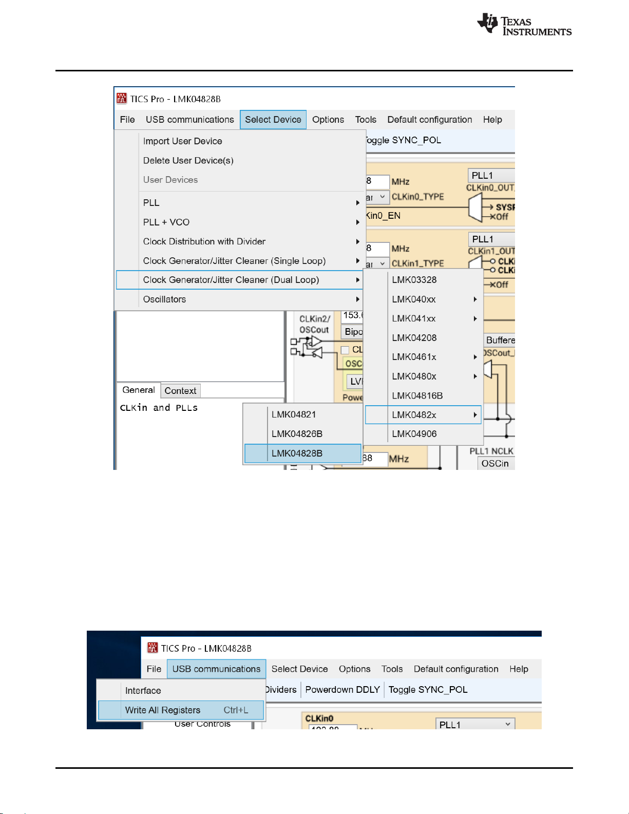
a. Select LMK04828B or LMK04826B from the “Select Device” Menu. Click “Select Device” → “Clock
Generator/ Jitter Cleaner (Dual Loop)” → “LMK0482x”.
b. Select USB2ANY mode from the Communication Setup window. To access this, select “USB
communications” → “Interface”. Confirm PC to USB communications by clicking “Identify” to see
blinking green LED on USB2ANY.
c. Select a default mode from the “Default configuration” Menu. For the quick start use, “CLKin1
122,88 MHz, OSCin 122.88 MHz”.
d. Ctrl+L must be pressed at least once to load all registers. Alternatively click “USB
communications” → “Write All Registers” or the “Write All Registers” button on the Raw Registers
page.
5. Measurements may be made at an active CLKout port through its SMA connector.
www.ti.com
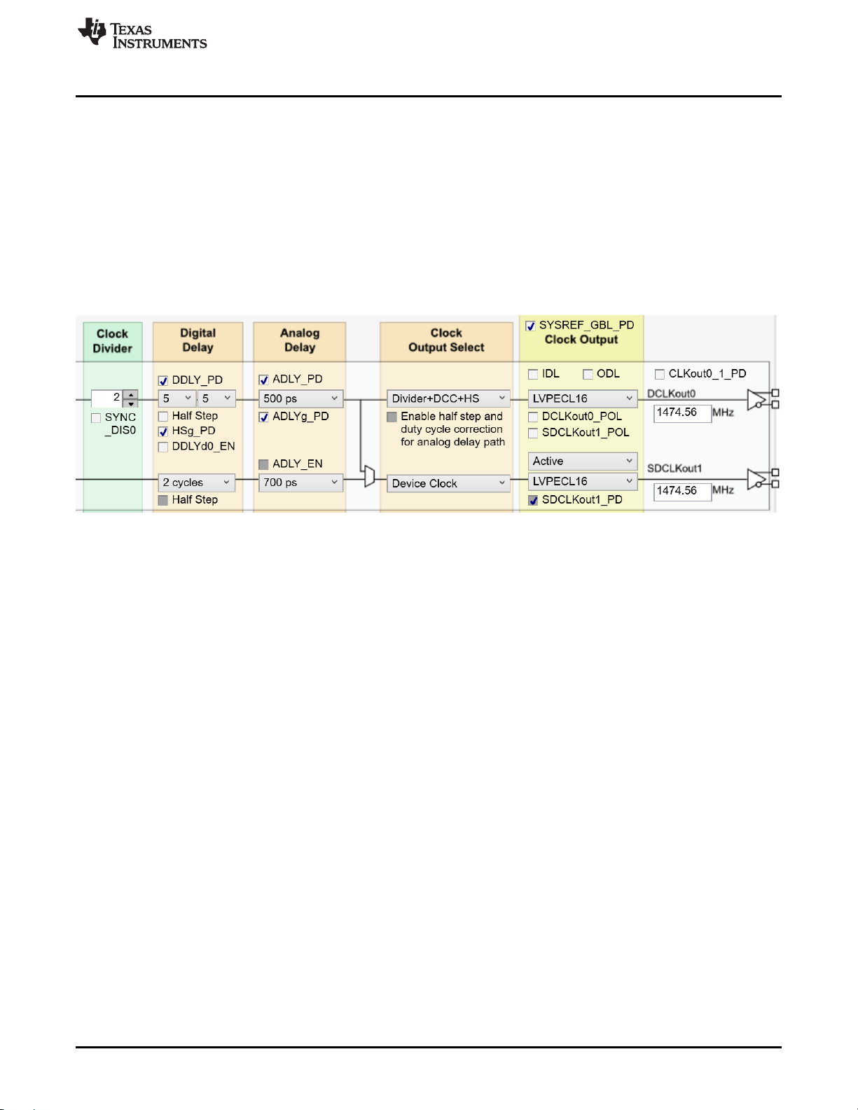
2.1.1 CLKout Page Description
Figure 2. CLKout Page Description Diagram
1. SYNC_DISX: Prevent the divider from being reset by SYNC/SYSREF path.
2. DCLKX_DIV: Divide value for the device clock. If set to 1 then #11 on list must = 1 and #12 must be
Divider+DCC+HS.
3. DDLYdX_EN: Enable dynamic digital delay for this divider.
4. DCLKX_HSg_PD: If clear, glitchless half-step adjustments are enabled.
5. DCLKX_HS: Set half step for this divider. #12 must be Divider+DCC+HS.
6. DCLKX_DDLY_PD: If clear, the digital delay value is assured when a SYNC occurs.
7. DCLKoutX_DDLY_CNTL/CNTH: for controlling the digital delay value.
4
LMK04826 and LMK04828 User’s Guide
Copyright © 2013–2018, Texas Instruments Incorporated
SNAU145B–MAY 2013–Revised March 2018
Submit Documentation Feedback
Page 5

www.ti.com
8. DCLKoutX_ADLYg_PD: If set, power down device clock glitchless analog delay feature.
9. DCLKoutX_ADLY_PD: If set, power down device clock analog delay.
10. DCLKoutX_ADLY: Analog delay (if enabled with #12).
11. DCLKoutX_ADLY_MUX: Enable duty cycle correct and half-step for this device clock divider.
12. DCLKoutX_MUX: Select source for CLKoutX. Can be Divider only, Divider+DCC+HS, Bypass, or
13. SDCLKoutY_POL: If set, polarity of SYSREF output clock is inverted.
14. DCLKoutX_POL: If set, polarity of device clock is inverted.
15. SYSREF_GBL_PD: Set the conditional for SDCLKoutY_DIS_MODE registers.
16. CLKoutX_Y_IDL: Increase input drive level to improve noise floor at cost of power.
17. CLKoutX_Y_ODL: Increase output drive level to improve noise floor at cost of power. No effect for
18. DCLKoutX_FMT: Set the clock output format for CLKoutX.
19. CLKoutX_Y_PD: Power down the entire CLKoutX_Y clock pair.
20. SDCLKoutY_DDLY: The SYSREF clock digital delay setting.
21. SDCLKoutY_HS: Set half step for the SYSREF output.
22. SDCLKoutY_ADLY_EN: Enable analog delay for the SYSREF clock path.
23. SDCLKoutY_ADLY: If enabled, set the analog delay for the SYSREF clock path.
24. SDCLKoutY_MUX: Select device clock or SYSREF clock path for CLKoutY.
25. SDCLKoutY_DIS_MODE: Set the output state of output clock drivers for the SYSREF clock. For
26. SDCLKoutY_FMT: Set the clock output format for CLKoutY.
27. SDCLKoutY_PD: Power down the SYSREF clock path.
28. Clock output frequency for CLKoutX and CLKoutY.
Quick Start
Analog Delay+Divider.
CLKoutX in bypass mode.
values of 1 and 2 works in conjunction with control on this list #15, SYSREF_GBL_PD.
NOTE: Setting a register equal to 0 OR un-checking a register’s checkbox performs the same
action. Similarly, setting a register equal to 1 is the same as checking that register’s
checkbox.
2.1.2 TICS Pro Tips
• Mousing over different controls will display some help prompt with the register address, data bit
location/length, and a brief register description in the lower left Context help pane.
2.2 SYSREF Quick Start
The LMK0482x EVK allows for verification of the LMK0482x’s implementation of JESD 204B SYSREF
functionality. To quickly setup and operate the SYSREF functions, refer to the following procedures.
2.2.1 Continuous SYSREF
1. On the Clock Outputs page, set SDCLKoutY_PD = 0 (where Y is the desired SDCLKout).
2. Set SDCLKoutY_MUX = 1 (Set to “SYSREF” for desired SDCLKout).
3. On the SYNC/SYSREF page, set SYSREF_PD and SYSREF_DDLY_PD = 0.
4. Set SYNC_DISX and SYNC_DISSYSREF = 0 (where X is the desired DCLKout).
5. Perform a SYNC event (toggle SYNC_POL on/off/on).
6. Set SYNC_DISX = 1 (for desired DCLKout’s) and SYNC_DISSYSREF = 1.
7. Set SYSREF_MUX = 3 (SYSREF Continuous).
8. Ensure SYSREF_CLR = 0 (On the right side, in the grey Other SYNC Controls box).
SNAU145B–MAY 2013–Revised March 2018
Submit Documentation Feedback
LMK04826 and LMK04828 User’s Guide
Copyright © 2013–2018, Texas Instruments Incorporated
5
Page 6
Quick Start
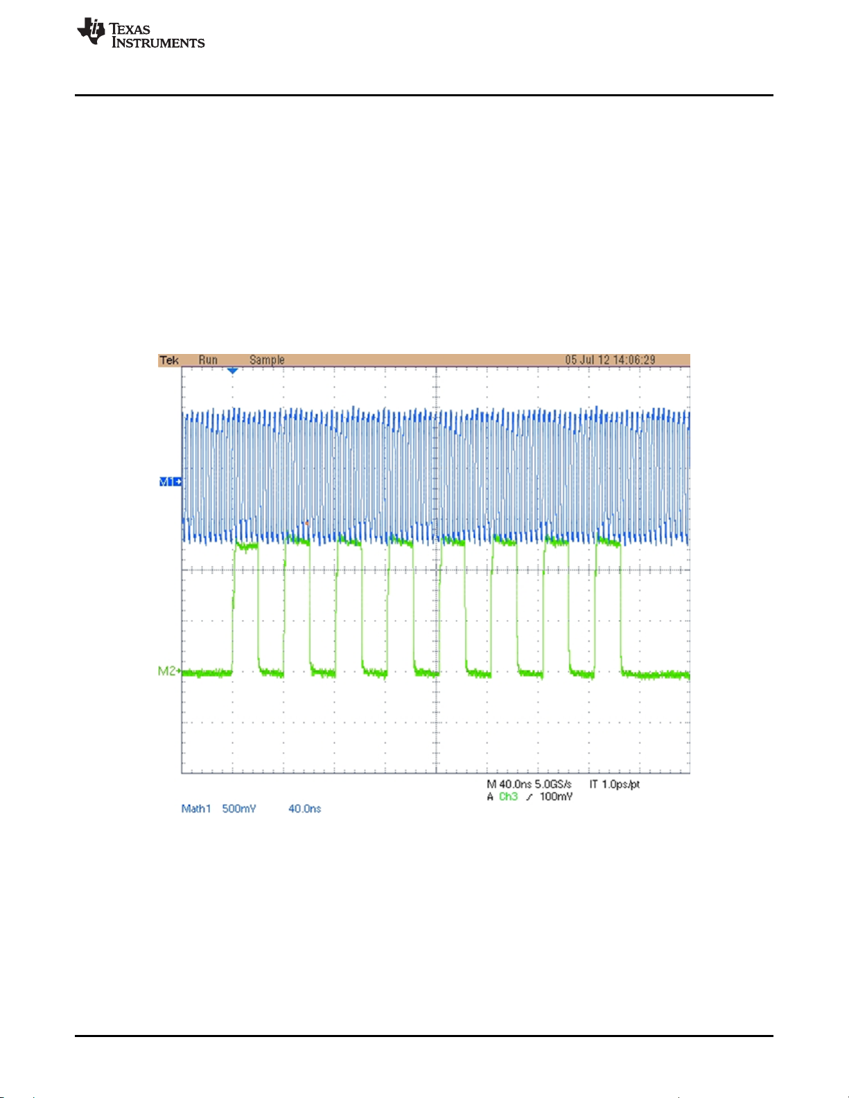
In Figure 3 and Figure 4, the Blue trace is DCLKout6 at 245.76 MHz and the Green trace is SDCLKout7
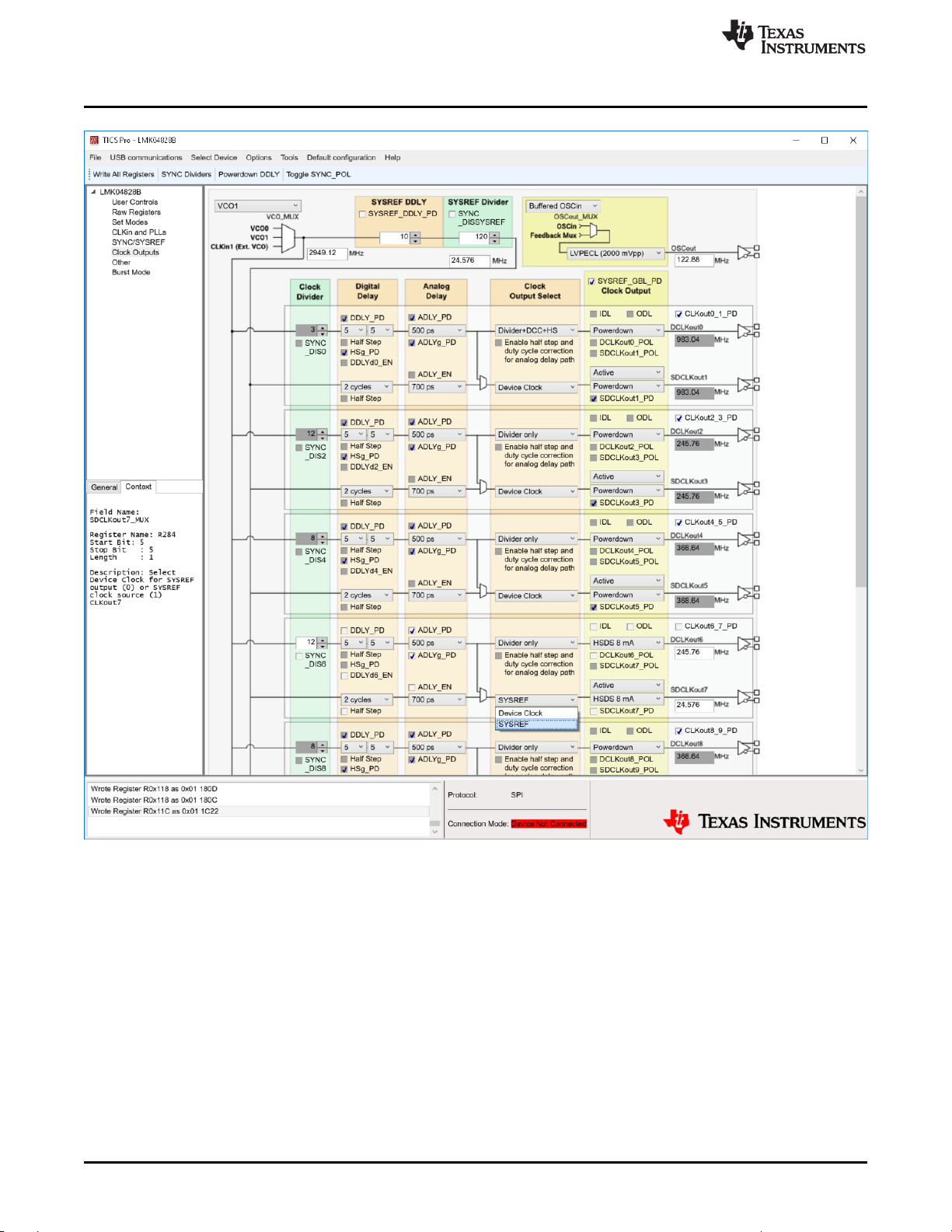
(SYSREF) at 24.475 MHz. Figure 5 shows the configuration of the LMK0482xB outputs.
www.ti.com
Figure 3. Continuous SYSREF Output
6
LMK04826 and LMK04828 User’s Guide
Copyright © 2013–2018, Texas Instruments Incorporated
SNAU145B–MAY 2013–Revised March 2018
Submit Documentation Feedback
Page 7
www.ti.com
2.2.2 Pulsed SYSREF
1. On the Clock Outputs page, set SDCLKoutY_PD = 0 (where Y is the desired SDCLKout).
2. Set SDCLKoutY_MUX = 1 (Set to “SYSREF” for desired SDCLKout).
3. On the SYNC/SYSREF page, set SYSREF_PD and SYSREF_DDLY_PD = 0.
4. Set SYNC_DISX and SYNC_DISSYSREF = 0 (where X is the desired DCLKout).
5. Set SYSREF_PLSR_PD = 0.
6. Perform a SYNC event (toggle SYNC_POL on/off/on).
7. Set SYNC_DISX = 1 (for desired DCLKout’s) and SYNC_DISSYSREF = 1.
8. Set SYSREF_MUX = 2 (SYSREF Pulser).
9. Set SYSREF_PULSE_CNT = 1, 2, 4, or 8 as desired.
10. Perform a SYNC event (toggle SYNC_POL on/off/on).
11. Ensure SYSREF_CLR = 0 (On the right side, in the grey Other SYNC Controls box).
Quick Start
SNAU145B–MAY 2013–Revised March 2018
Submit Documentation Feedback
Figure 4. Pulsed SYSREF Output
LMK04826 and LMK04828 User’s Guide
Copyright © 2013–2018, Texas Instruments Incorporated
7
Page 8
Quick Start
www.ti.com
Figure 5. Clock Outputs Page Setup for SYSREF Output on SDCLKout7
8
LMK04826 and LMK04828 User’s Guide
Copyright © 2013–2018, Texas Instruments Incorporated
SNAU145B–MAY 2013–Revised March 2018
Submit Documentation Feedback
Page 9
www.ti.com
3 PLL Loop Filters and Loop Parameters
In jitter cleaning applications that use a cascaded or dual PLL architecture, the first PLL’s purpose is to
substitute the phase noise of a low-noise oscillator (VCXO or crystal resonator) for the phase noise of a
“dirty” reference clock. The first PLL is typically configured with a narrow loop bandwidth to minimize the
impact of the reference clock phase noise. The reference clock consequently serves only as a frequency
reference rather than a phase reference.
The loop filters on the LMK048xx evaluation board are setup using the approach above. The loop filter for
PLL1 has been configured for a narrow loop bandwidth (> 100 kHz). The specific loop bandwidth values
depend on the phase noise performance of the oscillator mounted on the board. Table 2 and Table 3
contain the parameters for PLL1 and PLL2 for each oscillator option.
TI’s Clock Design Tool can be used to optimize PLL phase noise/jitter for given specifications. See:
http://www.ti.com/tool/clockdesigntool.
3.1 PLL1 Loop Filter
PLL Loop Filters and Loop Parameters
Table 2. PLL1 Loop Filter Parameters for Crystek 122.88 MHz VCXO
Phase Margin 50˚ Kφ (Charge Pump) 150 µA
Loop Bandwidth 14 Hz Phase Detector Freq 1.024 MHz
Reference Clock Frequency 122.88 MHz Output Frequency 122.88 MHz
Loop Filter Components C1_A1 = 100 nF C2_A1 = 680 nF R2_A1 = 39 kΩ
(1)
Loop Bandwidth is a function of Kφ, Kvco, N as well as loop components. Changing Kφ and N will change the loop bandwidth.
3.2 PLL2 Loop Filter
C1_A2 0.047 nF
C2_A2 3.9 nF
C3 (internal) 0.01 nF
C4 (internal) 0.01 nF
R2_A2 0.62 kΩ
R3 (internal) 0.2 kΩ
R4 (internal) 0.2 kΩ
Charge Pump Current, Kφ 3.2 mA
Phase Detector Frequency 122.88 MHz
Frequency 1966.08 2457.6 2457.6 2949.12 MHz
Kvco 15.3 8.9 21.9 17.4 MHz/V
N 16 20 20 24
Phase Margin 73 64 73 70 degrees
Loop Bandwidth 303 151 344 233 kHz
(1)
PLL Loop Bandwidth is a function of Kφ, Kvco, N as well as loop components. Changing Kφ and N will change the loop
bandwidth.
122.88 MHz VCXO PLL
VCO Gain 2.0 kHz/V
(To PLL 2)
Table 3. Integrated VCO PLL
LMK04826 LMK04828
VCO0 VCO1 VCO0 VCO1
(1)
(1)
SNAU145B–MAY 2013–Revised March 2018
Submit Documentation Feedback
LMK04826 and LMK04828 User’s Guide
Copyright © 2013–2018, Texas Instruments Incorporated
9
Page 10
Default TICS Pro Modes for the LMK0482x
4 Default TICS Pro Modes for the LMK0482x
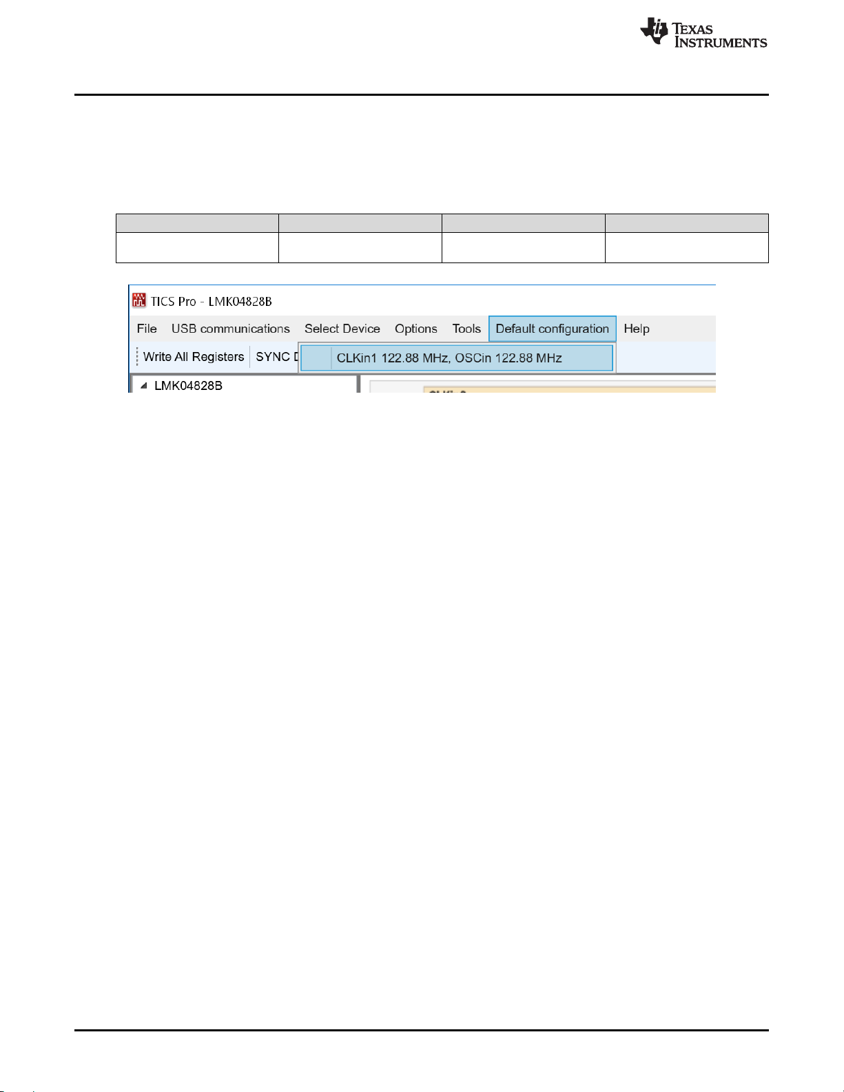
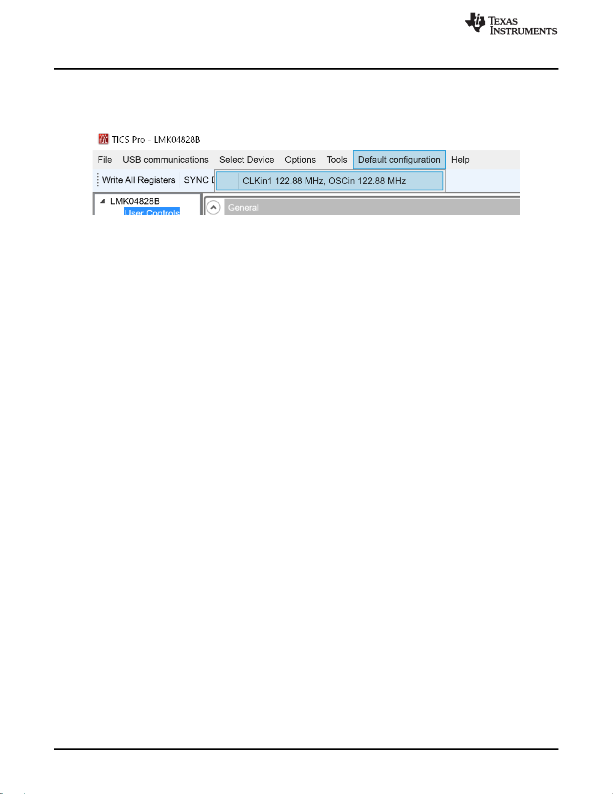
TICS Pro saves the state of the selected LMK0482x device when exiting the software. To ensure a
common starting point, the following modes listed in Table 4 may be restored by clicking “Default
configuration” and selecting the appropriate device configuration.
Table 4. Default TICS Pro Modes for the LMK0482x
Default TICS Pro Mode Device Mode CLKin Frequency OSCin Frequency
CLKin1 122.88 MHz, OSCin
122.88 MHz
Figure 6. Selecting a Default Mode for the LMK04828 Device
Dual PLL, Internal VCO 122.88 MHz 122.88 MHz
www.ti.com
10
LMK04826 and LMK04828 User’s Guide
Copyright © 2013–2018, Texas Instruments Incorporated
SNAU145B–MAY 2013–Revised March 2018
Submit Documentation Feedback
Page 11

www.ti.com
5 Using TICS Pro to Program the LMK0482x
This section will demonstrate how to use TICS Pro. Making measurements with the LMK04828B device
will serve as an example. For more information on using TICS Pro, refer to Appendix A. TICS Pro is
available for download at http://www.ti.com/tool/ticspro-sw.
Another option is to use CodeLoader4. The tool page for CodeLoader4 is located at
http://www.ti.com/tool/codeloader/.
Before proceeding, be sure to follow the instructions in Section 2 to ensure proper connections. To
program the LMK04826B, the procedure would be the same, but the LMK04826B would be selected as
the device.
5.1 Start TICS Pro Application
Click “Start” → “Programs” → “Texas Instruments” → “TICS Pro”.
The TICS Pro program is installed by default to the Texas Instruments application group.
5.2 Select Device
Click “Select Device” → “Clock Generator/ Jitter Cleaner (Dual Loop)” → “LMK0482x” → “LMK04828B”
Once started, TICS Pro will load the last used device. To load a new device, click “Select Device” from the
menu bar, then select the subgroup “Clock Generator/ Jitter Cleaner (Dual Loop)”, then “LMNK0482x”,
and finally the device to load. For this example, the LMK04828B is chosen. Selecting the device does
cause the device to be programmed. However, it is advisable to press “Ctrl+L”to ensure programming.
Using TICS Pro to Program the LMK0482x
SNAU145B–MAY 2013–Revised March 2018
Submit Documentation Feedback
LMK04826 and LMK04828 User’s Guide
Copyright © 2013–2018, Texas Instruments Incorporated
11
Page 12
Using TICS Pro to Program the LMK0482x
www.ti.com
5.3 Program/Load Device
Press “Ctrl+L”
Alternatively, click “USB communications” → “Write All Registers” from the menu to program the device to
the current state of the newly loaded LMK04828 file. “Ctrl+L” is the accelerator key assigned to the “Write
All Registers” option and is very convenient.
Once the device has been loaded, by default TICS Pro will automatically program changed registers, so it
is not necessary to load the device again completely. It is possible to disable this functionality by ensuring
there is no checkmark by the “Options” → “AutoUpdate”.
12
LMK04826 and LMK04828 User’s Guide
Figure 7. Selecting the LMK04828B
Figure 8. Loading the Device
Copyright © 2013–2018, Texas Instruments Incorporated
SNAU145B–MAY 2013–Revised March 2018
Submit Documentation Feedback
Page 13

www.ti.com
Once the device has been initially loaded, TICS Pro will automatically program changed registers, so it is
not necessary to reload the device upon subsequent changes in the device configuration. It is possible to
disable this functionality by ensuring there is no checkmark by the “Options” → “AutoUpdate”
Because a default mode will be restored in the next step, this step isn’t really needed but is included to
emphasize the importance of pressing “Ctrl+L” to load the device at least once after starting TICS Pro,
restoring a mode, or restoring a saved setup using the File menu.
Using TICS Pro to Program the LMK0482x
SNAU145B–MAY 2013–Revised March 2018
Submit Documentation Feedback
LMK04826 and LMK04828 User’s Guide
Copyright © 2013–2018, Texas Instruments Incorporated
13
Page 14
Using TICS Pro to Program the LMK0482x
5.4 Restoring a Default Mode
Click “Default configuration” → “CLKin1 122,88 MHz, OSCin 122.88 MHz”; then
Press “Ctrl+L”
Figure 9. Setting the Default Mode for LMK04828
For the purpose of this walkthrough, a default mode will be loaded to ensure a common starting point.
This is important because when TICS Pro is closed, it remembers the last settings used for a particular
device. Again, remember to press “Ctrl+L” as the first step after loading a default mode.
5.5 Visual Confirmation of Frequency Lock
After a default mode is restored and loaded, LED D4, and D5 must illuminate when PLL1 and PLL2 are
locked to the reference clock applied to CLKin1. This assumes PLL1_LD_MUX = PLL1_DLD,
PLL2_LD_MUX = PLL2_DLD and PLLX_LD_TYPE = Output (Push-Pull).
www.ti.com
14
LMK04826 and LMK04828 User’s Guide
Copyright © 2013–2018, Texas Instruments Incorporated
SNAU145B–MAY 2013–Revised March 2018
Submit Documentation Feedback
Page 15
www.ti.com
5.6 Enable Clock Outputs
While the LMK0482x offers programmable clock output buffer formats, the evaluation board is shipped
with pre-configured output terminations to match the default buffer type for each output.
To measure Phase noise at one of the clock outputs, for example DCLKout0:
1. Click on the Clock Outputs page,
2. Uncheck “CLKoutX_Y_PD” in the Clock Output box to enable the channel,
3. Set the following as needed:
a. Digital Delay value.
b. Clock Divider value (if “Bypass” is not selected as DCLKoutX_MUX).
c. Analog Delay Value (if “Analog Delay and Divider” is selected as DCLKoutX_MUX).
Using TICS Pro to Program the LMK0482x
Figure 10. Setting Digital Delay, Clock Divider, Analog Delay and Output Format
4. Depending on the configured output type, the clock output SMAs can be interfaced to a test instrument
with a single-ended 50-Ω input as follows.
a. For LVDS:
i. A balun (like ADT2-1T or high quality Prodyn BIB-100G) is recommended for differential-to-
single-ended conversion.
b. For LVPECL:
I. A balun can be used, or
II. One side of the LVPECL signal can be terminated with a 50-Ω load and the other side can be
run single-ended to the instrument.
c. For HSDS:
I. A balun (like ADT2-1T or high quality Prodyn BIB-100G) is recommended for differential-to-
single-ended conversion.
5. The phase noise may be measured with a spectrum analyzer or signal source analyzer.
TI’s Clock Design Tool can be used to calculate divider values to achieve desired clock output
frequencies. See: http://www.ti.com/tool/clockdesigntool
SNAU145B–MAY 2013–Revised March 2018
Submit Documentation Feedback
LMK04826 and LMK04828 User’s Guide
Copyright © 2013–2018, Texas Instruments Incorporated
15
Page 16
Evaluation Board Inputs and Outputs
6 Evaluation Board Inputs and Outputs
Table 5 contains descriptions of the inputs and outputs for the evaluation board. Unless otherwise noted,
the connectors described can be assumed to be populated by default. Additionally, some applicable TICS
Pro programming controls are noted for convenience.
Table 5. Description of Evaluation Board Inputs and Outputs
www.ti.com
CONNECTOR NAME
Populated:
DCLKout0,
DCLKout0*,
SDCLKout1,
SDCLKout1*,
DCLKout2,
DCLKout2*,
SDCLKout3,
SDCLKout3*,
DCLKout10,
DCLKout10*
SDCLKout11,
SDCLKout11*
Populated:
OSCout, OSCout*
V
CC
Populated:
J1
VccVCXO/Aux
SIGNAL TYPE,
INPUT/OUTPUT
Analog,
Output
Analog,
Output
Power,
Input
Power,
Input
Power,
Input
DESCRIPTION
Clock outputs with programmable output buffers.
The output terminations by default on the evaluation board are shown below:
Clock Output Pair Default Board Termination
DCLKout0 240 Ω
SDCLKout1 240 Ω
DCLKout2 240Ω
SDCLKout3 240 Ω
DCLKout4 HSDS / LVDS
SDCLKout5 HSDS / LVDS
DCLKout6 HSDS / LVDS
SDCLKout7 HSDS / LVDS
DCLKout8 HSDS / LVDS
SDCLKout9 HSDS / LVDS
DCLKout10 HSDS / LVDS
SDCLKout11 HSDS / LVDS
DCLKout12 HSDS / LVDS
SDCLKout13 HSDS / LVDS
Each CLKout pair has a programmable LVDS, LVPECL, or HSDS buffer. The
output buffer type can be selected in TICS Pro in the Clock Outputs page through
the CLKoutX_TYPE control.
All clock outputs are AC-coupled to allow safe testing with RF test equipment.
All LVPECL clock outputs are terminated using 240 Ω emitter-resistors.
If an output pair is programmed to LVCMOS, each output can be independently
configured (normal, inverted, or off/tri-state).
Buffered outputs of OSCin port.
The output terminations on the evaluation board are shown below.:
OSC Output Pair Default Board Termination
OSCout LVPECL
OSCout has a programmable LVDS, LVPECL, or LVCMOS output buffer. The
OSCout buffer type can be selected in TICS Pro on the Clock Outputs page
through the OSCout_FMT control.
OSCout is AC-coupled to allow safe testing with RF test equipment.
The OSCout output is terminated using 240 Ω emitter-resistors.
If OSCout is programmed as LVCMOS, each output can be independently
configured (normal, inverted, inverted, and off/tri-state).
Best performance/EMI reduction is achieved by using a complementary output
mode like Norm/Inv. It is NOT recommended to use Norm/Norm or Inv/Inv mode.
Main power supply input for the evaluation board.
The LMK0482x contains internal voltage regulators for the VCO, PLL and other
internal blocks. The clock outputs do not have an internal regulator, so a clean
power supply with sufficient output current capability is required for optimal
performance.
On-board LDO regulators and 0 Ω resistor options provide flexibility to supply and
route power to various devices. See the schematics in Appendix C for more details.
Alternative power supply input for the evaluation board using two unshielded wires
(Vcc and GND).
Apply power to either Vcc SMA or J1, but not both.
Optional Vcc input to power the VCXO circuit if separated voltage rails are needed.
The VccVCXO/Aux input can power these circuits directly or supply the on-board
LDO regulators. 0 Ω resistor options provide flexibility to route power.
16
LMK04826 and LMK04828 User’s Guide
SNAU145B–MAY 2013–Revised March 2018
Submit Documentation Feedback
Copyright © 2013–2018, Texas Instruments Incorporated
Page 17

www.ti.com
Table 5. Description of Evaluation Board Inputs and Outputs (continued)
CONNECTOR NAME
Populated:
CLKin0, CLKin0*,
CLKin1*
Not Populated:
CLKin1
Populated:
OSCin, OSCin*
Test point:
VTUNE1_TP
Test point:
VTUNE2_TP
Test points:
SDIO
SCK
CS*
Populated:
SPI
Test point:
Status_LD1_TP
Status_LD
Test point:
Status_LD2_TP
Status_LD2
Evaluation Board Inputs and Outputs
SIGNAL TYPE,
INPUT/OUTPUT
Analog,
Input
Analog,
Input
Analog,
Input
Analog,
Input
CMOS,
Input/Output 10-pin header for SPI programming interface and programmable logic I/O pins for
CMOS,
Input/Output
CMOS,
Input/Output
Reference Clock Inputs for PLL1 (CLKin0, 1). CLKin1 can alternatively be used as
an External Feedback Clock Input (FBCLKin) in 0-delay mode or an RF Input (Fin)
in External VCO mode.
Reference Clock Inputs for PLL1 (CLKin0, 1)
FBCLKin/CLKin1* is configured by default for a single-ended reference clock input
from a 50-ohm source. The non-driven input pin (FBCLKin/CLKin1) is connected to
GND with a 0.1 µF. CLKin0/CLKin0* is configured by default for a differential
reference clock input from a 50-ohm source.
CLKin1* is the default reference clock input selected in TICS Pro. The clock input
selection mode can be programmed on the Set Modes page through the
LMK0482x Sub-Modes.
External Feedback Input (FBCLKin) for 0-Delay
CLKin1 is shared for use with FBCLKin as an external feedback clock input to PLL1
for 0-delay mode. See the LMK04820 family datasheet (literature number
SNAS605) for more details on using 0-delay mode with the evaluation board and
the evaluation board software.
Feedback VCXO clock input to PLL1 and Reference clock input to PLL2.
The single-ended output of the onboard VCXO (U4) drives the OSCin* input of the
device and the OSCin input of the device is connected to GND with 0.1 µF.
A VCXO add-on board may be optionally attached through these SMA connectors
with minor modification to the components going to the OSCin/OSCin* pins of
device. This is useful if the VCXO footprint does not accommodate the desired
VCXO device or if the user desires to use the LMK0482xB in single loop mode.
A single-ended or differential signal may be used to drive the OSCin/OSCin* pins
and must be AC coupled. If operated in single-ended mode, the unused input must
be connected to GND with 0.1 µF.
Refer to the LMK04820 family datasheet section “Electrical Characteristics” for
PLL2 Reference Input (OSCin) specifications (literature number SNAS605).
Tuning voltage output from the loop filter for PLL1.
If a VCXO add-on board is used, this tuning voltage can be connected to the
voltage control pin of the external VCXO when this SMA connector is installed and
connected through R72 by the user.
Tuning voltage output from the loop filter for PLL2.
the LMK0482x.
10-pin header for SPI programming interface and programmable logic I/O pins for
the LMK0482x.
The programmable logic I/O signals accessible through this header include:
RESET, SYNC, Status_LD1, Status_LD2, CLKin_SEL0, and CLKin_SEL1. These
logic I/O signals also have dedicated SMAs and test points.
Programmable status output pin. By default, set to output the digital lock detect
status signal for PLL1.
In the default TICS Pro modes, LED D5 will illuminate green when PLL1 lock is
detected by the LMK0482x (output is high) and turn off when lock is lost (output is
low).
The status output signal for the Status_LD1 pin can be selected on the User
Controls page through the PLL1_LD_MUX control.
Programmable status output pin. By default, set to output the digital lock detect
status signal for PLL2.
In the default TICS Pro modes, LED D4 will illuminate green when PLL1 lock is
detected by the LMK0482x (output is high) and turn off when lock is lost (output is
low).
The status output signal for the Status_LD1 pin can be selected on the User
Controls page through the PLL2_LD_MUX control.
DESCRIPTION
SNAU145B–MAY 2013–Revised March 2018
Submit Documentation Feedback
Copyright © 2013–2018, Texas Instruments Incorporated
LMK04826 and LMK04828 User’s Guide
17
Page 18

Evaluation Board Inputs and Outputs
Table 5. Description of Evaluation Board Inputs and Outputs (continued)
CONNECTOR NAME
Test points:
CLKin0_SEL_TP
CLKin1_SEL_TP
Test point:
SYNC_TP
Populated:
SYNC
Test point:
RESET_TP
SIGNAL TYPE,
INPUT/OUTPUT
Input/Output
Input/Output
Input/Output
CMOS,
CMOS,
CMOS,
www.ti.com
DESCRIPTION
Programmable status I/O pins. By default, set as input pins for controlling input
clock switching of CLKin0 and CLKin1.
These inputs will not be functional because CLKin_SEL_MODE is set to 0 (CLKin0
Manual) by default in the User Controls page in TICS Pro. To enable input clock
switching, CLKin_SEL_MODE must be 3 and Status_CLKinX_TYPE must be 0 to 2
(pin enabled as an input).
Input Clock Switching – Pin Select Mode
When CLKin_SEL_MODE is 3, the Status_CLKinX pins select which clock input is
active as follows:
Status_CLKin1 Status_CLKin0 Active Clock
0 0 CLKin0
0 1 CLKin1
1 0 CLKin2
1 1 Holdover
Programmable status I/O pin. By default, set as an input pin for synchronize the
clock outputs with a fixed and known phase relationship between each clock output
selected for SYNC. A SYNC event also causes the digital delay values to take
effect.
SYNC/SYSREF_REQ pin forces the SYSREF_MUX into SYSREF Continuous
mode (0x03) when SYSREF_REQ_EN = 1.
SYNC/SYSREF_REQ pin can hold outputs in a low state, depending on system
configuration. SYNC_POL adjusts for active low or active high control.
A SYNC event can also be programmed by toggling the SYNC_POL bit in the User
Controls page in TICS Pro.
Programmable status I/O pin.
18
LMK04826 and LMK04828 User’s Guide
Copyright © 2013–2018, Texas Instruments Incorporated
SNAU145B–MAY 2013–Revised March 2018
Submit Documentation Feedback
Page 19

www.ti.com
7 Recommended Test Equipment
Power Supply
The Power Supply must be a low noise power supply, particularly when the devices on the board are
being directly powered (onboard LDO regulators bypassed).
Phase Noise / Spectrum Analyzer
To measure phase noise and RMS jitter, an Agilent E5052 Signal Source Analyzer is recommended. An
Agilent E4445A PSA Spectrum Analyzer with the Phase Noise option is also usable although the
architecture of the E5052 is superior for phase noise measurements. At frequencies less than 100 MHz
the local oscillator noise of the E4445A is too high and measurements will reflect the E4445A’s internal
local oscillator performance, not the device under test.
Oscilloscope
To measure the output clocks for AC performance, such as rise time or fall time, propagation delay, or
skew, it is suggested to use a real-time oscilloscope with at least 1 GHz analog input bandwidth (2.5+
GHz recommended) with 50-Ω inputs and 10+ Gsps sample rate. To evaluate clock synchronization or
phase alignment between multiple clock outputs, it is recommended to use phase-matched, 50-Ω cables
to minimize external sources of skew or other errors/distortion that may be introduced if using oscilloscope
probes.
Recommended Test Equipment
SNAU145B–MAY 2013–Revised March 2018
Submit Documentation Feedback
LMK04826 and LMK04828 User’s Guide
Copyright © 2013–2018, Texas Instruments Incorporated
19
Page 20

TICS Pro is used to program the evaluation board with the USB2ANY interface adapter. TICS Pro can
also be used to generate register maps for programming the device and current consumption estimates.
This appendix outlines the basic purpose and usage of each page. TICS Pro is available for download at:
http://www.ti.com/tool/ticspro-sw.
A.1 TICS Pro Tips
Mousing over different controls will display some help prompt with the register address, data bit
location/length, and a brief register description in the lower left Context help pane.
A.2 Communication Setup
The Communication Setup window allows the USB2ANY or DemoMode to be selected. In case multiple
evaluation boards are to be connected and run with multiple instances of TICS Pro, the drop-down box will
allow specific USB2ANY devices to be selected. Pressing the identify button will identify which USB2ANY
is currently selected. Devices used by other instances of TICS Pro won’t display in this list.
Appendix A
SNAU145B–MAY 2013–Revised March 2018
TICS Pro Usage
20
TICS Pro Usage
Copyright © 2013–2018, Texas Instruments Incorporated
SNAU145B–MAY 2013–Revised March 2018
Submit Documentation Feedback
Page 21

www.ti.com
A.3 User Controls
The User Controls page has controls not included on one of the later discussed dedicated pages.
User Controls
Figure 11. TICS Pro - User Controls Page
SNAU145B–MAY 2013–Revised March 2018
Submit Documentation Feedback
Copyright © 2013–2018, Texas Instruments Incorporated
TICS Pro Usage
21
Page 22

Raw Registers Page
A.4 Raw Registers Page
The Raw Register page displays the register map including address. The address bits have the shaded
background and are not editable. The unshaded bits are the data bits. This register map may be directly
manipulated by clicking into the bit field, moving around with the arrow keys, and typing ‘1’ or ‘0’ to change
a bit.
All registers may be read or written in addition to individual registers. For individual register read/write, the
active register is highlighted in the list of registers and displayed in the top right. An individual register or
field may be read back by entering the name into the bottom right and clicking the “Read” button.
Register maps may be exported, but also imported. The import format may simply be the address and
register data in hex format as illustrated in the address/value column, one register to a line.
www.ti.com
22
TICS Pro Usage
Figure 12. TICS Pro - Raw Registers Page
SNAU145B–MAY 2013–Revised March 2018
Copyright © 2013–2018, Texas Instruments Incorporated
Submit Documentation Feedback
Page 23

www.ti.com
A.5 Set Modes Page
The Set Modes page allows the user to quickly configure the LMK0482x into a desired mode. If the
LMK0482x is already in the desired mode, or several registers already programmed as needed, the log
won’t display any or many register writes.
The top LMK0482x modes section allows the user to set high level usage profiles to allow the device to
operate in dual loop, single loop, or distribution mode.
The bottom LMK0482x sub-modes section allows further JESD204B configuration, 0-delay configuration,
or clock input configuration which may apply for many of the LMK0482x modes of operation.
Set Modes Page
SNAU145B–MAY 2013–Revised March 2018
Submit Documentation Feedback
Figure 13. TICS Pro - Set Modes Page
Copyright © 2013–2018, Texas Instruments Incorporated
TICS Pro Usage
23
Page 24

CLKinX and PLLs Page
A.6 CLKinX and PLLs Page
The CLKinX and PLLs page allows entry of the input frequency at the different CLKinX pins, the mode by
which the active CLKinX is selected, where the CLKinX inputs are routed to.
This page also illustrates the frequencies that the PLL1 and PLL2 operate at. In distribution mode, the
CLKin1 frequency will directly be connected to the VCO/clock distribution path frequency. In addition to
the basic PLL dividers and controls, when the PLLX_NCLK_MUX selects the feedback mux as a source,
0-delay modes are achieved. When enabling 0-delay red text will help guide the user through properly
setting up 0-delay mode.
When using dual PLL mode, the OSCin Source combo box can be set to “External VCXO” which links the
OSCin frequency with the external VCXO frequency. When using single PLL2 mode, the OSCin Source
combo box can be set to “Independent” to allow the OSCin frequency to be unlinked from the external
VCXO frequency.
www.ti.com
24
TICS Pro Usage
Figure 14. TICS Pro - CLKinX Control Page
SNAU145B–MAY 2013–Revised March 2018
Copyright © 2013–2018, Texas Instruments Incorporated
Submit Documentation Feedback
Page 25

www.ti.com
A.7 SYNC / SYSREF Page
The SYNC / SYSREF page allows some mode set buttons for JESD204B features. The SYNC dividers
button will stop all SYNC inputs, set normal SYNC mode, enable all dividers for SYNC, issue a SYNC by
toggling SYNC_POL, set all dividers to ignore SYNC, then return any other changed parameter to its
original state. This is a nice feature to ensure all outputs are synchronized together or to be run after
changing the digital delay value which requires a SYNC to update. This functionality is also available on
any other page through the toolbar as “SYNC Dividers.”
NOTE: To use SYNC or SYSREF, ensure that SYNC_EN = 1. To use SYSREF in continuous,
pulser, or re-clocked modes, be sure SYSREF_PD = 0.
The SCLKX_Y_DIS_MODE bits allow the clock outputs to be disabled or set to a low state. Because
values 1 and 2 are only conditionally set by the SYSREF_GBL_PD bit, it is possible to power up/down
several SYSREF outputs by programming only one register. When changing between 0x00 (Active) and
(0x01) Conditional Low, keeping the SYSREF_CLR = 1 during transition will prevent glitch pulses from the
SYSREF output.
SYNC / SYSREF Page
Figure 15. TICS Pro - SYNC / SYSREF Page
SNAU145B–MAY 2013–Revised March 2018
Submit Documentation Feedback
Copyright © 2013–2018, Texas Instruments Incorporated
TICS Pro Usage
25
Page 26

Clock Outputs Page
A.8 Clock Outputs Page
The Clock Outputs page allows control of all the clock outputs format and other options relating to the
clock outputs. All the clock outputs are paired and allow two device clocks, two SYSREF clocks, or one of
each. The naming convention uses X_Y for controls which can impact both CLKoutX (even clock) and
CLKoutY (odd clock), X for controls impacting only CLKoutX and Y for controls impacting only CLKoutY.
www.ti.com
26
TICS Pro Usage
Figure 16. TICS Pro - Clock Outputs Page
SNAU145B–MAY 2013–Revised March 2018
Copyright © 2013–2018, Texas Instruments Incorporated
Submit Documentation Feedback
Page 27

www.ti.com
A.9 Other Page
The Other page contains some registers to control the GPIO pins of the LMK0482x. Each pin has two
fields, the first is the _TYPE field which allows the input or output mode of the pin to be defined. The
second is the _MUX field which, when set for output, controls what the pin will output.
Other Page
SNAU145B–MAY 2013–Revised March 2018
Submit Documentation Feedback
Figure 17. TICS Pro - Other Page
Copyright © 2013–2018, Texas Instruments Incorporated
TICS Pro Usage
27
Page 28

Burst Page
A.10 Burst Page
The Burst page allows the user to program sequences of register programming or pin control.
www.ti.com
Figure 18. TICS Pro - Burst Page
28
TICS Pro Usage
Copyright © 2013–2018, Texas Instruments Incorporated
SNAU145B–MAY 2013–Revised March 2018
Submit Documentation Feedback
Page 29

Appendix B
SNAU145B–MAY 2013–Revised March 2018
Typical Phase Noise Performance Plots
The LMK0482x’s dual PLL architecture achieves ultra low jitter and phase noise by allowing the external
VCXO or Crystal’s phase noise to dominate the final output phase noise at low offset frequencies and the
internal VCO’s phase noise to dominate the final output phase noise at high offset frequencies. This
results in the best overall noise and jitter performance.
Table 6 lists the test conditions used for output clock phase noise measurements with the Crystek 122.88
MHz VCXO.
Table 6. LMK0482x Test Conditions
PARAMETER VALUE
PLL1 Reference clock input CLKin1* single-ended input, CLKin1 AC-coupled to GND
PLL1 Reference Clock frequency 122.88 MHz
PLL1 Phase detector frequency 1024 kHz
PLL1 Charge Pump Gain 150 µA
VCXO frequency 122.88 MHz
PLL2 phase detector frequency 122.88 MHz
PLL2 Charge Pump Gain 3200 µA
PLL2 REF2X mode Enabled
SNAU145B–MAY 2013–Revised March 2018
Submit Documentation Feedback
Copyright © 2013–2018, Texas Instruments Incorporated
Typical Phase Noise Performance Plots
29
Page 30

VCXO Phase Noise 122.88 MHz
B.1 VCXO Phase Noise 122.88 MHz
The phase noise of the reference is masked by the phase noise of this VCXO by using a narrow loop
bandwidth for PLL1 while retaining the frequency accuracy of the reference clock input. This VCXO sets
the reference noise to PLL2. Figure 19 shows the open loop typical phase noise performance of the
CVHD-950-122.88 Crystek VCXO.
Figure 19. Crystek CVHD-950-122.88 MHz VCXO Phase Noise at 122.88 MHz
www.ti.com
Table 7. VCXO Phase Noise and Jitter
Offset
10 Hz -76.6 515.4
100 Hz -108.9 60.5
1 kHz -137.4 36.2
10 kHz -153.3 35
100 kHz -162 34.5
1 MHz -165.7 32.9
10 MHz -168.1 22.7
40 MHz -168.1 —
VCXO Phase Noise
at 122.88 MHz (dBc/Hz)
B.2 Output Measurement Technique
The same technique was used to measure phase noise for all three output types available on the
programmable OSCout and CLKout buffers. This was achieved by terminating one side of the LVPECL,
LVDS, or LVCMOS output with a 50-Ω load, and measuring the other side single-ended using an Agilent
E5052B Source Signal Analyzer.
B.3 Clock Outputs (DCLKout and SDCLKout)
The LMK0482x features programmable HSDS, LVDS, LVPECL buffer modes for the DCLKoutX,
SDCLKout pairs. Below is a phase noise measurement of DCLKout2 (best phase noise clock output)
using both a balun and single ended.
VCXO RMS Jitter to High Offset
of 20 MHz at 122.88 MHz (rms fs)
30
Typical Phase Noise Performance Plots
Copyright © 2013–2018, Texas Instruments Incorporated
SNAU145B–MAY 2013–Revised March 2018
Submit Documentation Feedback
Page 31

www.ti.com
Clock Outputs (DCLKout and SDCLKout)
Figure 20. LMK04826 DCLKout2, VCO0, 245.76 MHz, Div8, LVPECL20 /w
240-Ω Emitter Resistor, DCLKoutX_MUX=Divider, IDL=1, ODL=0, Balun = Prodyn BIB-100G
SNAU145B–MAY 2013–Revised March 2018
Submit Documentation Feedback
Copyright © 2013–2018, Texas Instruments Incorporated
Typical Phase Noise Performance Plots
31
Page 32

Clock Outputs (DCLKout and SDCLKout)
www.ti.com
32
Figure 21. LMK04826 DCLKout2, VCO0, 245.76 MHz, Div8, LVPECL20 /w
240-Ω Emitter Resistor, DCLKoutX_MUX=Divider, IDL=1, ODL=0, Single Ended
Typical Phase Noise Performance Plots
Copyright © 2013–2018, Texas Instruments Incorporated
SNAU145B–MAY 2013–Revised March 2018
Submit Documentation Feedback
Page 33

www.ti.com
Clock Outputs (DCLKout and SDCLKout)
Figure 22. LMK04826 DCLKout2, VCO1, 245.76 MHz, Div10, LVPECL20 /w
240 ohm emitter resistor, DCLKoutX_MUX=Divider, IDL=1, ODL=0, Balun = Prodyn BIB-100G
SNAU145B–MAY 2013–Revised March 2018
Submit Documentation Feedback
Copyright © 2013–2018, Texas Instruments Incorporated
Typical Phase Noise Performance Plots
33
Page 34

Clock Outputs (DCLKout and SDCLKout)
www.ti.com
34
Figure 23. LMK04826 DCLKout2, VCO1, 245.76 MHz, Div10 , LVPECL20 /w
240-Ω Emitter Resistor, DCLKoutX_MUX=Divider, IDL=1, ODL=0, Single Ended
Typical Phase Noise Performance Plots
Copyright © 2013–2018, Texas Instruments Incorporated
SNAU145B–MAY 2013–Revised March 2018
Submit Documentation Feedback
Page 35

www.ti.com
Clock Outputs (DCLKout and SDCLKout)
Figure 24. LMK04828 DCLKout2, VCO0, 245.76 MHz, Div10, LVPECL20 /w
240-Ω Emitter Resistor, DCLKoutX_MUX=Divider, IDL=1, ODL=0, Balun = ADT2-1T
SNAU145B–MAY 2013–Revised March 2018
Submit Documentation Feedback
Copyright © 2013–2018, Texas Instruments Incorporated
Typical Phase Noise Performance Plots
35
Page 36

Clock Outputs (DCLKout and SDCLKout)
www.ti.com
36
Figure 25. LMK04828 DCLKout2, VCO0, 245.76 MHz, Div10, LVPECL20 /w
240-Ω Emitter Resistor, DCLKoutX_MUX=Divider, IDL=1, ODL=0, Single Ended
Typical Phase Noise Performance Plots
Copyright © 2013–2018, Texas Instruments Incorporated
SNAU145B–MAY 2013–Revised March 2018
Submit Documentation Feedback
Page 37

www.ti.com
Clock Outputs (DCLKout and SDCLKout)
Figure 26. LMK04828 DCLKout2, VCO1, 245.76 MHz, Div12, LVPECL20 /w
240-Ω Emitter Resistor, DCLKoutX_MUX=Divider, IDL=1, ODL=0, Balun = ADT2-1T
SNAU145B–MAY 2013–Revised March 2018
Submit Documentation Feedback
Copyright © 2013–2018, Texas Instruments Incorporated
Typical Phase Noise Performance Plots
37
Page 38

Clock Outputs (DCLKout and SDCLKout)
www.ti.com
38
Figure 27. LMK04828 DCLKout2, VCO1, 245.76 MHz, Div12, LVPECL20 /w
240-Ω Emitter Resistor, DCLKoutX_MUX=Divider, IDL=1, ODL=0, Single Ended
Typical Phase Noise Performance Plots
Copyright © 2013–2018, Texas Instruments Incorporated
SNAU145B–MAY 2013–Revised March 2018
Submit Documentation Feedback
Page 39

Appendix C
SNAU145B–MAY 2013–Revised March 2018
Schematics
SNAU145B–MAY 2013–Revised March 2018
Submit Documentation Feedback
Copyright © 2013–2018, Texas Instruments Incorporated
Schematics
39
Page 40

VccPLLPlane
0.1µF
C335
DNP
120 FB
R326
DNP
120 FB
R330
DNP
VccCLKoutPlane
120 FB
R328
DNP
0.1µF
C329
DNP
Power Plane for LMK Except Outputs
Power Planes for LMK Outputs
Vcc
VccAuxPlane
VccCLKoutPlane
VccPLLPlane
Direct Power - NO Regulators
120 FB
R343
VccAuxPlane
IN
4
ADJ
6
GND
3
NC
7
SD
8
DAP
9
OUT
5
BYP1NC
2
U302
LP3878SD-ADJ/NOPB
LP3878-ADJ 3.3 V component values:
C340 = 4.7 uF
R350= 51 k
C346 = 0.01 uF R356=866
C352 = 10 uF
R351= 2.00 k
C341 = 2.2 nF
0.01µF
C323
0.1µF
C322
1µF
C321
1µF
C347
0
R332
1
1
2
2
J1
TERMBLOCK_2
IN6OUT
1
GND
3
EN
4
NC
5
DAP
7
NC
2
U305
LP5900SD-3.3/NOPB
GND
V_LM3878-ADJ
C359 = 0.47 uF
C360 = 0.47 uF
R369 = 51 k
LP3878SD-ADJ
LP5900SD-3.3
LP5900 Component values
0
R100
0
R327
0
R329
0
R331
0
R346
120 FB
R345
0
R106
120 FB
R347
0.1µF
C312
1µF
C311
10µF
C310
0.1µF
C319
1µF
C318
10µF
C317
0.1µF
C326
1µF
C325
10µF
C324
Aux Power for XO/VCXO, Status LEDs
0.01µF
C315
1µF
C314
10µF
C313
1µF
C337
Vcc2_CG1
Vcc1_VCO
Vcc5_DIG
Vcc9_CP2
Vcc6_PLL1
Vcc7_OSCout
Vcc8_OSCin
Vcc10_PLL2
CG3
CG0
CG2
CG1
Vcc12_CG0
VCO
Digital
CP2
PLL1
OSCout
OSCin
PLL2
0
R349
120 FB
R358
1
234
5
Vcc
142-0701-201
Vcc_VCO
1
2
VccVCO/Aux
142-0711-201
DNP
VccAuxPlane
0
R229
DNP
0
R337
120 FB
R342
LDO_Out_LP3878
TESTPOINT
VccTP
TESTPOINT
0.1µF
C316
DNP
0.1µF
C320
DNP
100pF
C327
DNP
0.1µF
C328
DNP
100pF
C332
DNP
0.1µF
C334
DNP
0.1µF
C336
DNP
51k
R350
0.1µF
C346
2.00k
R351
866
R356
51k
R369
0.47µF
C359
0.47µF
C360
0
R54
DNP
4.7µF
C340
1µF
C342
2200pF
C341
0
R105
1
2
VccVCXO/Aux
142-0711-201
DNP
0
R352
DNP
VccAuxPlane
Vcc11_CG3
0
R101
Vcc4_CG2
1µF
C364
1µF
C343
120 FB
R354
120 FB
R371
0
R364
IN6OUT
1
GND
3
EN
4
NC
5
DAP
7
NC
2
U303
LP5900SD-3.3/NOPB
GND
C359 = 0.47uF
C360 = 0.47uF
R369 = 51 k
LP5900SD-3.3
LP5900 Component values
51k
R360
0.47µF
C350
0.47µF
C351
VccLDOin
0
R363
DNP
0
R367
DNP
Vcc_VCO_LDO
0
R373
0
R368
DNP
0
R370
DNP
Vcc_VCXO_LDO
Vcc_VCXO
0
R19
Switch resistor
for power.
10µF
C352
VccPLLPlane
VccCLKoutPlane
0.1µF
C361
DNP
Regulator to power VCO Separately
Regulator to power VCXO Separately
LDO for powering LMK04828
0
R310
0
R323
0
R334
0
R340
0
R339
0
R338
0
R335
0
R107
SYSREF
Vcc3_SYSREF
1µF
C300
120 FB
R344
OUT
1
OUT
2
FB
3
GND
4
NC
5
RT/CLK
6
PGND
7
PGND
8
PVIN
9
PVIN
10
VSENSE12COMP
13
SS
14
EN
15
PH
16
PH
17
BOOT
18
PWRGD
19
NC
20
LDOEN
21
NR
22
LDOIN
24
VIN
11
LDOIN
23
DAP
0
U301
TPS54120RGYR
DNP
0
R377
DNP
10µF
C370
DNP
40.2k
R365
DNP
0
R378
DNP
0.01µF
C371
DNP
2.2k
R380
DNP
0.047µF
C373
DNP
330pF
C372
DNP
0.1µF
C358
DNP
47µF
C363
DNP
100pF
C362
DNP
0.1µF
C369
DNP
41.2k
R366
DNP
10k
R379
DNP
10µF
C356
DNP
0.1µF
C355
DNP
0.1µF
C357
DNP
0
R362
DNP
30.9k
R311
DNP
0.1µF
C354
DNP
10k
R361
DNP
0.01µF
C353
DNP
4.7µF
C333
DNP
100µF
C331
DNP
GND
DC-DC to LDO to Power LMK04828
22µH
L300
744031220
DNP
GND GND
GND
GND
GND
GND
0
R74
DNP
120 FB
R305
120 FB
R307
GND
0
R95
120
R333
120
R341
Vcc2_CG1_1
Vcc4_CG2_1
Vcc11_CG3_1
Vcc12_CG0_1
Vcc3_SYSREF_1
Vcc9_CP2_1
Vcc10_PLL2_1
Vcc8_OSCin_1
Vcc7_OSCout_1
Vcc6_PLL_1
Vcc5_DIG_1
Vcc1_VCO_1
GND_TP
TESTPOINT
0
R336
Power Supply
C.1 Power Supply
40
Schematics
www.ti.com
SNAU145B–MAY 2013–Revised March 2018
Submit Documentation Feedback
Copyright © 2013–2018, Texas Instruments Incorporated
Page 41

100pF
C2pA2
DNP
0.1µF
C36
DNP
0.1µF
C27
0
R55
Y301
DNP
DNP
0
R69
DNP
PLL2 Loop Filters
Y300
DNP
DNP
VTUNE2_TP
VCXO-mode Loop Filter
10µF
C35
0.1µF
C37
DCLKout0_P
DCLKout0_N
SDCLKout1_P
SDCLKout1_N
SDCLKout3_P
SDCLKout3_N
DCLKout2_N
DCLKout2_P
SDCLKout5_P
SDCLKout5_N
DCLKout4_N
DCLKout4_P
CLKin0_P
CLKin0_N
CLKin1_P
CLKin1_N
Status_LD2
DCLKout12_P
DCLKout12_N
SDCLKout13_N
SDCLKout13_P
SDCLKout11_P
SDCLKout11_N
DCLKout10_N
DCLKout10_P
DCLKout8_P
DCLKout8_N
SDCLKout9_N
SDCLKout9_P
SYNC
0
R60
DNP
SDIO
SCK
CS*
OSCout_N
OSCout_P
Vcc1_VCO
Vcc2_CG1
Vcc3_SYSREF Vcc4_CG2
Vcc6_PLL1
Vcc7_OSCout
Vcc10_PLL2
Vcc11_CG3
Vcc12_CG0
Vcc8_OSCin
SYNC
Status_LD2
CLKin_SEL0CLKin_SEL1
CS*
SDIO
SCK
12pF
C33
0
R53
DNP
DNP
Cb1_VCO
DNP
DNP
Cb2pVCO
DNP
DNP
Rb2_VCO
DNP
DNP
Cb2_VCO
DNP
0
R304
DNP
0.1µF
C38
51
R61
51
R68
620
R2_A2
47pF
C1_A2 3900pF
C2_A2
CPout1
Vcc9_CP2
51
R376
DNP
Status_LD1
SDCLKout7_N
DCLKout6_P
DCLKout6_N
SDCLKout7_P
Status_LD1
RESET
RESET
OSCin VCXO
120
R10
DNP
120
R16
DNP
0
R21
DNP
100
R4
0
R23
DNP
0
R1
DNP
0
R12
33pF
C4
0.1µF
C8
DNP
1
234
5
OSCin*
142-0701-806
1
234
5
OSCin
142-0701-806
Switch resistor for signal
(shared pad) [C4 and R1]
Switch resistor for signal
(shared pad) [C8 and R23]
0.1µF
C301
DNP
0
R301
DNP
10k
R302
DNP
10k
R303
DNP
Vcc_VCO_OpAmp
0
R300
DNP
Vcc_VCO_OpAmp
4
3
2
1
5
V+
V-
U300
LMP7731MF
DNP
PLL2 External VCO Loop Filter
Vcc_VCO_LDO
0.1µF
C303
DNP
0.1µF
C302
DNP
0
R353
DNP
0
R33
DNP
0
R25
DNP
0.1µF
C12
DNP
100pF
C17
DNP
Vcc_VCO
0
R22
DNP
VCC_VCO_TP
GND
3
Vtune
2
GND
1
GND7Mod6GND5GND
8
GND4GND
9
Fout
10
GND
11
GND
12
GND
13
Vcc
14
GND15GND
16
U3
CRO2949A-LF
DNP
0
R29
DNP
VCO_Fout
PLL2_Vtune_AF
0
C13
18
R24
DNP
270
R26
DNP
0.1µF
C18
0.1µF
C19
0
R30
0
C20
0.1µF
C16
DNP
100pF
C15
DNP
0.1µF
C14
DNP
270
R27
DNP
270
R32
DNP
1
234
5
FBCLKin*/CLKin1*
142-0701-806
1
234
5
FBCLKin/CLKin1
142-0701-806
DNP
100
R28
DNP
0
R230
DNP
51
R45
51
R56
DNP
VCO_Fout
CLKin1
PLL2_Vtune_AF
0
R3
270
R7
DNP
0.1µF
C2
0.1µF
C6
270
R6
DNP
0.1µF
C3
DNP
100
R9
0
R11
0
C5
270
R17
DNP
0.1µF
C7
DNP
1
234
5
CLKin0*
142-0701-806
1
234
5
CLKin0
142-0701-806
0
R2
0
R13
51
R8
DNP
CLKin0_2_N
51
R14
DNP
270
R15
DNP
51
R5
DNP
0
C1
51
R35
DNP
51
R38
DNP
FBCLKin/CLKin1 Impedance Matching and Attenuation
CLKin0 Impedance Matching and Attenuation
CLKin0_2_P
51
R382
DNP
Vcc5_DIG
270
R31
DNP
2200pF
C375
2200pF
C32
2pF
C374
2pFC34
4.70k
R62
4.70k
R381
10k
R308
DNP
1000pF
C304
0
R65
DNP
P
1
NC
2
PD3S
4
SCT
5
SD
6
B1
BALUN -A DT2-1T+
DNP
GND
3
GND
2
Vt
1
GND
7
GND6GND
5
RFout
8
GND
4
GND
9
GND
10
Vcc
11
GND
12
U5
DNP
OSCin_P
OSCin_N
OSCin_1_N
OSCin_1_P
Vtune
1
NC
2
GND3RF
4
RF*
5
Vs
6
U2
CVHD-950-122.88
GND_VCXO
0
R375
120 FB
R374
120 FB
R18
10uF
C11
2200pF
C10
82pF
C9
VCC_VCXO_TP
GND_VCXO
0.1uF
C367
100pF
C368
GND_VCXO
Vcc_VCXO
100pF
C3_AB1
0
R3_AB1
GND_VCXO
0
R44
DNP
0
R43
DNP
0
R20
DNP
DCLKout0
1
DCLKout0*
2
SDCLKout1*
4
SDCLKout1
3
RESET
5
SYNC
6
NC
7
NC
8
NC
9
Vcc1_VCO
10
LDObyp1
11
LDObyp2
12
SCK19SDIO20SDCLKout522Vcc3_SYSREF21SDCLKout5*23DCLKout424DCLKout4*25Vcc4_CG226DCLKout627DCLKout6*28SDCLKout729SDCLKout7*
30
CLKin1*/Fin*/FBCLKin*
35
Vcc6_PLL1
36
CLKin0
37
CLKin0*
38
Vcc7_OSCout
39
OSCout0
40
OSCout*
41
Vcc8_OSCin
42
OSCin
43
OSCin*
44
Vcc9_CP2
45
CPout2
46
DCLKout8
51
DCLKout8*
52
Vcc11_CG3
53
DCLKout10
54
DCLKout10*
55
SDCLKout11
56
SDCLKout11*
57
CLKin_SEL058CLKin_SEL1
59
SDCLKout13
60
SDCLKout13*
61
DCLKout12
62
LMK04828
DAPPAD
0
SDCLKout3
13
SDCLKout3*
14
DCLKout2
15
DCLKout2*
16
Vcc2_CG117CS*
18
Status_LD131CPout1
32
Vcc5_DIG
33
CLKin1/Fin/FBCLKin
34
Vcc10_PLL2
47
Status_LD2
48
SDCLKout9
49
SDCLKout9*
50
DCLKout12*
63
Vcc12_CG0
64
U1
LMK04828
U7 is alternate footprint for 5x3.2 mm VCXO package
D6
SMV1249-079LF
D1
SMV1249-079LF
Vtune
1
NC
2
GND3RF
4
RF*
5
Vs
6
U7
DNP
0.01µF
C28
DNP
Note: CVHD-950-### is a 4 pin part but with 200 mil pin spa cings. So pin
mapping from 6 pin (schematic) to 4 pin footprint is:
1 --> 1, 3 --> 2, 4 --> 3, 6 --> 4
This arrangement also allows for many differen tial VCXOs to also be used
Assembly Note
ZZ1 U2 and U7: 4 pin and 6 pin footprints are compatible
0
R306
DNP
0.68uF
C2_A1
PLL1 Loop Filter
VCXO Loop Filter
VTUNE1_TP
0
R78
DNP
Vcc_VCXO_OpAmp
4
3
2
1
5
V+
V-
U4
LMP7731MF
DNP
Vcc_VCXO_LDO
0
R75
0.1µF
C41
DNP
0.1µF
C1_A1
2.7µF
C2pA1
DNP
39k
R2_A1
0
R36
DNP
0
R34
DNP
100pF
C29
33pF
C305
DNP
33pF
C330
DNP
470pF
C338
DNP
www.ti.com
LMK04828B
C.2 LMK04828B
SNAU145B–MAY 2013–Revised March 2018
Submit Documentation Feedback
Copyright © 2013–2018, Texas Instruments Incorporated
Schematics
41
Page 42

Status_LD2_TP
TESTPOINT
100pF
C42
DNP
27k
R87
DNP
100pF
C43
DNP
0
R84
SPI HEADER
Status_LD1
Status_LD2
SYNC Level Translation
CLKin Select 0
270
R93
DNP
12
34
56
78
910
SPI
HEADER_2X5
15k
R315
27k
R316
SDIO
TESTPOINT
27k
R322
DNP
CS*
TESTPOINT
15k
R321
SYNC_TP
TESTPOINT
100pF
C309
DNP
Status_LD1_TP
TESTPOINT
0
R82
27k
R86
CLKIN0_SEL_TP
TESTPOINT
CLKIN1_SEL_TP
TESTPOINT
270
R79
DNP
27k
R319 27k
R320
15k
R317
15k
R318
SYNC
CLKin_SEL1CLKin_SEL0
Status_LD2
Status_LD1
270
R83
270
R85
SCK
SDIO
CS*
27k
R325
15k
R324
1
2
SYNC
142-0711-201
DNP
1
2
Status_LD2
142-0711-201
DNP
1
2
Status_LD1
142-0711-201
DNP
15k
R81
15k
R80
DNP
D5
Green
D2
Red
D3
Red
RESET
CLKin Select 1
100pF
C306
DNP
SCK
TESTPOINT
27k
R313
15k
R312
100pF
C308
DNP
100pF
C307
DNP
27k
R50
27k
R51
DNP
27k
R57
DNP
VccPLLPlane
VccPLLPlane
VccPLLPlane
The pull-down resistors on CS*, SCK, SD IO
pins are to be used only in the cas e of 5V logic.
27k
R384
27k
R383
DNP
VccPLLPlane
RESET_TP
TESTPOINT
D4
Green
15k
R94
0
R113
0
R110
DNP
0
R109
0
R108
DNP
LOGO
PCB
Texas Instruments
LOGO
PCB
ESD Susceptible
SV600788
C
PCB Number:
PCB Rev:
VccPLLPlane
Shared pad
Shared pad
S1
0.375" StandoffS20.375" Standoff
S3
0.375" StandoffS40.375" Standoff
S5
0.375" StandoffS60.375" Standoff
GND GND
GNDGND
GND GND
Digital
C.3 Digital
www.ti.com
42
Schematics
SNAU145B–MAY 2013–Revised March 2018
Submit Documentation Feedback
Copyright © 2013–2018, Texas Instruments Incorporated
Page 43

0.1µF
C54
0.1µF
C58
SDCLKout3
0.1µF
C48
0.1µF
C52
SDCLKout1
SDCLKout1_P
SDCLKout1_N
SDCLKout3_P
SDCLKout3_N
1
234
5
SDCLKout3*
142-0701-806
1
234
5
SDCLKout3
142-0701-806
1
234
5
SDCLKout1*
142-0701-806
1
234
5
SDCLKout1
142-0701-806
SDCLKout1_1_P
SDCLKout1_1_N
SDCLKout3_1_P
SDCLKout3_1_N
51
R124
DNP
51
R138
DNP
51
R102
DNP
51
R117
DNP
240
R134
GND
240
R126
GND
240
R112
GND
240
R104
GND
0.1µF
C66
0.1µF
C70
SDCLKout7
0.1µF
C60
0.1µF
C64
SDCLKout5
SDCLKout5_N
SDCLKout5_P
SDCLKout7_N
SDCLKout7_P
1
234
5
SDCLKout5*
142-0701-806
DNP
1
234
5
SDCLKout5
142-0701-806
DNP
1
234
5
SDCLKout7*
142-0701-806
DNP
1
234
5
SDCLKout7
142-0701-806
DNP
SDCLKout7_1_P
SDCLKout7_1_N
SDCLKout5_1_P
SDCLKout5_1_N
51
R164
51
R182
51
R142
51
R158
240
R148
DNP
GND
240
R156
DNP
GND
240
R170
DNP
GND
240
R178
DNP
GND
0.1µF
C78
0.1µF
C82
SDCLKout11
0.1µF
C72
SDCLKout9
0.1µF
C76
SDCLKout9_1_P
SDCLKout9_1_N
SDCLKout9_P
SDCLKout9_N
SDCLKout11_P
SDCLKout11_N
1
234
5
SDCLKout9*
142-0701-806
DNP
1
234
5
SDCLKout9
142-0701-806
DNP
1
234
5
SDCLKout11*
142-0701-806
1
234
5
SDCLKout11
142-0701-806
SDCLKout11_1_P
SDCLKout11_1_N
51
R190
51
R206
51
R212
DNP
51
R228
DNP
240
R222
DNP
GND
240
R215
DNP
GND
240
R200
DNP
GND
240
R192
DNP
GND
0.1µF
C21
0.1µF
C25
SDCLKout13
SDCLKout13_P
SDCLKout13_N
1
234
5
SDCLKout13*
142-0701-806
DNP
1
234
5
SDCLKout13
142-0701-806
DNP
SDCLKout13_1_P
SDCLKout13_1_N
51
R37
51
R72240
R52
DNP
GND
240
R42
DNP
GND
SYSREF CLOCK OUTPUTS
560
R64
560
R66
560
R70
560
R67
100
R59
DNP
100
R58
DNP
560
R63
www.ti.com
C.4 Clock Outputs
C.4.1 Clock Outputs Page 1
Clock Outputs
SNAU145B–MAY 2013–Revised March 2018
Submit Documentation Feedback
Copyright © 2013–2018, Texas Instruments Incorporated
Schematics
43
Page 44

0.1µF
C59
0.1µF
C63
DCLKout4_N
DCLKout4_P
DCLKout4
0.1µF
C65
DCLKout6_N
DCLKout6_P
DCLKout6
0.1µF
C69
1
234
5
DCLKout4
142-0701-806
DNP
1
234
5
DCLKout4*
142-0701-806
DNP
1
234
5
DCLKout6
142-0701-806
DNP
1
234
5
DCLKout6*
142-0701-806
DNP
DCLKout6_1_P
DCLKout6_1_N
DCLKout4_1_P
DCLKout4_1_N
51
R141
51
R157
51
R163
51
R179
240
R169
DNP
GND
240
R177
DNP
GND
240
R155
DNP
GND
240
R147
DNP
GND
0.1µF
C44
0.1µF
C46
OSCout_N
OSCout_P
OSCout
OSCout_1_P
OSCout_1_N
1
234
5
OSCout
142-0701-806
1
234
5
OSCout*
142-0701-806
51
R90
DNP
51
R96
DNP
240
R231
GND
240
R232
GND
DCLKout0_N
DCLKout0_P
DCLKout0
1
234
5
DCLKout0
142-0701-806
1
234
5
DCLKout0*
142-0701-806
0.1µF
C47
0.1µF
C51
DCLKout0_1_P
DCLKout0_1_N
51
R99
DNP
51
R114
DNP
240
R103
GND
240
R111
GND
DCLKout2_P
DCLKout2_N
DCLKout2
0.1µF
C57
DCLKout2_1_N
DCLKout2_1_P
1
234
5
DCLKout2*
142-0701-806
1
234
5
DCLKout2
142-0701-806
0.1µF
C53
51
R121
DNP
51
R135
DNP
240
R125
GND
240
R133
GND
0.1µF
C77
0.1µF
C81
0.1µF
C71
0.1µF
C75
DCLKout8_N
DCLKout8_P
DCLKout8
DCLKout10
DCLKout10_N
DCLKout10_P
1
234
5
DCLKout8
142-0701-806
DNP
1
234
5
DCLKout8*
142-0701-806
DNP
1
234
5
DCLKout10
142-0701-806
1
234
5
DCLKout10*
142-0701-806
DCLKout10_1_P
DCLKout10_1_N
DCLKout8_1_P
DCLKout8_1_N
51
R209
DNP
51
R225
DNP
51
R187
51
R204
240
R191
DNP
GND
240
R199
DNP
GND
240
R213
DNP
GND
240
R221
DNP
GND
0.1µF
C22
0.1µF
C26
DCLKout12
DCLKout12_N
DCLKout12_P
1
234
5
DCLKout12
142-0701-806
DNP
1
234
5
DCLKout12*
142-0701-806
DNP
DCLKout12_1_P
DCLKout12_1_N
51
R41
51
R237
240
R46
DNP
GND
240
R77
DNP
GND
DEVICE CLOCK OUTPUTS AND OSCout
0
C24
0
C23
100
R40
DNP
OSCout_1_2_P
OSCout_1_2_N
100
R76
DNP
100
R71
DNP
560
R73
560
R91
560
R89560
R88
560
R92
Clock Outputs
C.4.2 Clock Outputs Page 2
www.ti.com
SNAU145B–MAY 2013–Revised March 2018
Submit Documentation Feedback
44
Schematics
Copyright © 2013–2018, Texas Instruments Incorporated
Page 45

Appendix D
SNAU145B–MAY 2013–Revised March 2018
Bill of Materials
D.1 Bill of Materials for LMK0482x
Table 8. Bill of Materials LMK0482x Evaluation Boards
ITEM DESIGNATOR DESCRIPTION MANUFACTURER PART NUMBER QTY.
1 PCB Printed Circuit Board Any SV600788C 1
C1, C5, C13, C20, C23,
C24, R3, R3_AB1, R11,
R12, R19, R30, R55,
R75, R82, R84, R95,
R109, R113, R310,
2
R323, R327, R329,
R331, R334, R335,
R336, R337, R338,
R339, R340, R346,
R349, R364, R373,
R375
C1_A1, C2, C6, C18,
C19, C21, C22, C25,
C26, C27, C38, C37,
C44, C46, C47, C48,
C51, C52, C53, C54,
3
C57, C58, C59, C60,
C63, C64, C65, C66,
C70, C71, C72, C75,
C76, C77, C78, C81,
C82, C312, C319, C346
C1_A2 CAP, CERM, 47pF, 50V,
4
C2_A1 CAP, CERM, 0.68µF,
5
C2_A2 CAP, CERM, 3900pF,
6
C3_AB1, C29, C368 CAP, CERM, 100pF,
7
C4 CAP, CERM, 33pF,
8
C9 CAP, CERM, 82pF, 50V,
9
C10, C32, C341, C375 CAP, CERM, 2200pF,
10
C11 CAP, CERM, 10µF, 10V,
11
C33 CAP, CERM, 12pF, 50V,
12
C34, C374 CAP, CERM, 2pF, 50V,
13
C35, C310, C317, C324,
14
C352
RES, 0 ohm, 5%, 0.1W,
0603
CAP, CERM, 0.1µF,
25V, +/-5%, X7R, 0603
+/-5%, C0G/NP0, 0603
10V, +/-10%, X5R, 0603
50V, +/-10%, X7R, 0603
50V, +/-5%, C0G/NP0,
0603
100V, +/-5%, C0G/NP0,
0603
+/-10%, C0G/NP0, 0603
50V, +/-10%, X7R, 0603
+/-20%, X5R, 0805
+/-5%, C0G/NP0, 0603
+/-12.5%, C0G/NP0,
0603
CAP, CERM, 10µF, 10V,
+/-10%, X5R, 0805
Vishay-Dale CRCW06030000Z0EA
Kemet C0603C104J3RACTU
Kemet C0603C470J5GACTU
Kemet C0603C684K8PACTU
MuRata GRM188R71H392KA01D
Kemet C0603C101J5GACTU
AVX 06031A330JAT2A
Kemet C0603C820K5GACTU
Kemet C0603C222K5RACTU
Kemet C0805C106M8PACTU
AVX 06035A120JAT2A
Kemet C0603C209C5GACTU
Kemet C0805C106K8PACTU
36
40
1
1
1
3
1
1
4
1
1
2
5
SNAU145B–MAY 2013–Revised March 2018
Submit Documentation Feedback
Copyright © 2013–2018, Texas Instruments Incorporated
Bill of Materials
45
Page 46

Bill of Materials for LMK0482x
www.ti.com
Table 8. Bill of Materials LMK0482x Evaluation Boards (continued)
ITEM DESIGNATOR DESCRIPTION MANUFACTURER PART NUMBER QTY.
C69, C322, C326, C367 CAP, CERM, 0.1µF,
15
C300, C311, C314,
C318, C321, C325,
16
C337, C342, C343,
C347, C364
C304 CAP, CERM, 1000pF,
17
C313 CAP, CERM, 10µF,
18
C315, C323 CAP, CERM, 0.01µF,
19
C340 CAP, CERM, 4.7µF,
20
C350, C351, C359,
21
C360
CLKin0, CLKin0*,
DCLKout0, DCLKout0*,
DCLKout2, DCLKout2*,
DCLKout10,
DCLKout10*,
FBCLKin*/CLKin1*,
OSCin, OSCin*,
22
OSCout, OSCout*,
SDCLKout1,
SDCLKout1*,
SDCLKout3,
SDCLKout3*,
SDCLKout11,
SDCLKout11*
D1, D6 DIODE VARACTOR 15V
23
D2, D3 LED 2.8X3.2MM 565NM
24
D4, D5 LED 2.8X3.2MM 565NM
25
J1 CONN TERM BLK PCB
26
R2, R13, R332 RES, 0 ohm, 5%,
27
R2_A1 RES, 39k ohm, 5%,
28
R2_A2 RES, 620 ohm, 5%,
29
R4, R9 RES, 100 ohm, 5%,
30
R18, R305, R307, R342,
R343, R344, R345,
31
R347, R354, R358,
R371, R374
R37, R41, R45, R61,
R68, R72, R141, R142,
R157, R158, R163,
32
R164, R179, R182,
R237, R187, R190,
R204, R206
R50, R86, R313, R316,
33
R319, R320, R325,
R384
25V, +/-10%, X7R, 0603
CAP, CERM, 1µF, 10V,
+/-10%, X5R, 0603
50V, +/-5%, C0G/NP0,
0603
6.3V, +/-20%, X5R, 0603
100V, +/-10%, X7R,
0603
10V, +/-10%, X5R, 0603
CAP, CERM, 0.47µF,
16V, +/-10%, X7R, 0603
Connector, SMT, End
launch SMA 50 ohm
20MA SC-79
RED CLR SMD
GRN CLR SMD
5.08MM 2POS OR
0.125W, 0805
0.1W, 0603
0.1W, 0603
0.1W, 0603
FB, 120 ohm, 500 mA,
0603
RES, 51 ohm, 5%, 0.1W,
0603
RES, 27k ohm, 5%,
0.1W, 0603
Kemet C0603C104K3RACTU
Kemet C0603C105K8PACTU
Kemet C0603C102J5GACTU
Kemet C0603C106M9PACTU
Kemet C0603C103K1RACTU
Kemet C0603C475K8PACTU
Kemet C0603C474K4RACTU
Emerson
Network Power
Skyworks Inc SMV1249-079LF
Lumex Opto/Components Inc. SML-LX2832IC
Lumex Opto/Components Inc. SML-LX2832GC
Weidmuller 1594540000
Vishay-Dale CRCW08050000Z0EA
Vishay-Dale CRCW060339K0JNEA
Vishay-Dale CRCW0603620RJNEA
Vishay-Dale CRCW0603100RJNEA
Murata BLM18AG121SN1D
Vishay-Dale CRCW060351R0JNEA
Vishay-Dale CRCW060327K0JNEA
142-0701-806
4
11
1
1
2
1
4
19
2
2
2
1
3
1
1
2
12
19
8
46
Bill of Materials
Copyright © 2013–2018, Texas Instruments Incorporated
SNAU145B–MAY 2013–Revised March 2018
Submit Documentation Feedback
Page 47

www.ti.com
Bill of Materials for LMK0482x
Table 8. Bill of Materials LMK0482x Evaluation Boards (continued)
ITEM DESIGNATOR DESCRIPTION MANUFACTURER PART NUMBER QTY.
R62, R381 RES, 4.70k ohm, 1%,
34
R63, R64, R66, R67,
35
R70, R73, R88, R89,
R91, R92
R81, R94, R312, R315,
36
R317, R318, R321,
R324
R83, R85 RES, 270 ohm, 5%,
37
R100, R101, R105,
38
R106, R107
R103, R104, R111,
R112, R125, R126,
39
R133, R134, R231,
R232
R333, R341 FB, 120 ohm, 500 mA,
40
R350, R360, R369 RES, 51k ohm, 5%,
41
R351 RES, 2.00k ohm, 1%,
42
R356 RES, 866 ohm, 1%,
43
44 S1, S2, S3, S4, S5, S6 0.375" Standoff VOLTREX SPCS-6 6
SPI Low Profile Vertical
45
46 U1
47 U2 122.88 MHz VCXO Crystek CVHD-950-122.88 1
U302 Micropower 800mA Low
48
U303, U305 Ultra Low Noise, 150mA
49
50 Vcc Connector, TH, SMA Emerson Network Power 142-0701-201 1
0.1W, 0603
RES, 560 ohm, 5%,
0.1W, 0603
RES, 15k ohm, 5%,
0.1W, 0603
0.1W, 0603
RES, 0 ohm, 5%,
0.063W, 0402
RES, 240 ohm, 5%,
0.1W, 0603
0402
0.1W, 0603
0.1W, 0603
0.1W, 0603
Header 2x5 0.100"
LMK04826
LMK04828 LMK04828BISQ
Noise "Ceramic Stable"
Adjustable Voltage
Regulator for 1V to 5V
Applications, 8-pin LLP,
Pb-Free
Linear Regulator for
RF/Analog Circuits
Requires No Bypass
Capacitor, 6-pin LLP,
Pb-Free
Yageo America RC0603FR-074K7L
Vishay-Dale CRCW0603560RJNEA
Vishay-Dale CRCW060315K0JNEA
Vishay-Dale CRCW0603270RJNEA
Vishay-Dale CRCW04020000Z0ED
Vishay-Dale CRCW0603240RJNEA
TDK MMZ1005Y121C
Vishay-Dale CRCW060351K0JNEA
Vishay-Dale CRCW06032K00FKEA
Vishay-Dale CRCW0603866RFKEA
FCI 52601-G10-8LF
Texas Instruments
Texas Instruments LP3878SD-ADJ/NOPB
Texas Instruments LP5900SD-3.3/NOPB
LMK04826BISQ
2
10
8
2
5
10
2
3
1
1
1
1
1
2
SNAU145B–MAY 2013–Revised March 2018
Submit Documentation Feedback
Copyright © 2013–2018, Texas Instruments Incorporated
Bill of Materials
47
Page 48

Revision History
www.ti.com
Revision History
NOTE: Page numbers for previous revisions may differ from page numbers in the current version.
Changes from A Revision (June 2013) to B Revision .................................................................................................... Page
• Deleted Appendices C - E that regarded obsolete pre-release boards with old interfaces...................................... 2
• Removed “-001 board” as it is obsolete and required older interface. ............................................................. 2
• Revised Section 2 for TICS Pro software and interface.............................................................................. 4
• Deleted Quick Start notes of obsolete pre-release boards that required old interfaces.......................................... 4
• Changed PLL Charge Pump gain to “150” from “450” µA and VCO Gain to “2” from “2.5” kHz/V. ............................ 9
• Revised Section 4 for TICS Pro software............................................................................................. 10
• Revised Section 5 for TICS Pro software............................................................................................. 11
• Changed Status_CLKinX_TYPE to “2” from “3”. .................................................................................... 18
• Moved Schematics and Bill of Materials to Appendices. ........................................................................... 19
• Revised Appendix Afor TICS Pro software. .......................................................................................... 20
• Changed PLL1 Charge Pump Gain to “150µA” from “450µA”. .................................................................... 29
• Changed “VCXO RMS Jitter to High Offset” column to correct values. .......................................................... 30
• Deleted Appendices C - E that regarded obsolete pre-release boards with old interfaces. ................................... 38
• Revised formatting for Table 8......................................................................................................... 45
48
Revision History
Copyright © 2013–2018, Texas Instruments Incorporated
SNAU145B–MAY 2013–Revised March 2018
Submit Documentation Feedback
Page 49

STANDARD TERMS FOR EVALUATION MODULES
1. Delivery: TI delivers TI evaluation boards, kits, or modules, including any accompanying demonstration software, components, and/or
documentation which may be provided together or separately (collectively, an “EVM” or “EVMs”) to the User (“User”) in accordance
with the terms set forth herein. User's acceptance of the EVM is expressly subject to the following terms.
1.1 EVMs are intended solely for product or software developers for use in a research and development setting to facilitate feasibility
evaluation, experimentation, or scientific analysis of TI semiconductors products. EVMs have no direct function and are not
finished products. EVMs shall not be directly or indirectly assembled as a part or subassembly in any finished product. For
clarification, any software or software tools provided with the EVM (“Software”) shall not be subject to the terms and conditions
set forth herein but rather shall be subject to the applicable terms that accompany such Software
1.2 EVMs are not intended for consumer or household use. EVMs may not be sold, sublicensed, leased, rented, loaned, assigned,
or otherwise distributed for commercial purposes by Users, in whole or in part, or used in any finished product or production
system.
2 Limited Warranty and Related Remedies/Disclaimers:
2.1 These terms do not apply to Software. The warranty, if any, for Software is covered in the applicable Software License
Agreement.
2.2 TI warrants that the TI EVM will conform to TI's published specifications for ninety (90) days after the date TI delivers such EVM
to User. Notwithstanding the foregoing, TI shall not be liable for a nonconforming EVM if (a) the nonconformity was caused by
neglect, misuse or mistreatment by an entity other than TI, including improper installation or testing, or for any EVMs that have
been altered or modified in any way by an entity other than TI, (b) the nonconformity resulted from User's design, specifications
or instructions for such EVMs or improper system design, or (c) User has not paid on time. Testing and other quality control
techniques are used to the extent TI deems necessary. TI does not test all parameters of each EVM.
User's claims against TI under this Section 2 are void if User fails to notify TI of any apparent defects in the EVMs within ten (10)
business days after delivery, or of any hidden defects with ten (10) business days after the defect has been detected.
2.3 TI's sole liability shall be at its option to repair or replace EVMs that fail to conform to the warranty set forth above, or credit
User's account for such EVM. TI's liability under this warranty shall be limited to EVMs that are returned during the warranty
period to the address designated by TI and that are determined by TI not to conform to such warranty. If TI elects to repair or
replace such EVM, TI shall have a reasonable time to repair such EVM or provide replacements. Repaired EVMs shall be
warranted for the remainder of the original warranty period. Replaced EVMs shall be warranted for a new full ninety (90) day
warranty period.
3 Regulatory Notices:
3.1 United States
3.1.1 Notice applicable to EVMs not FCC-Approved:
FCC NOTICE: This kit is designed to allow product developers to evaluate electronic components, circuitry, or software
associated with the kit to determine whether to incorporate such items in a finished product and software developers to write
software applications for use with the end product. This kit is not a finished product and when assembled may not be resold or
otherwise marketed unless all required FCC equipment authorizations are first obtained. Operation is subject to the condition
that this product not cause harmful interference to licensed radio stations and that this product accept harmful interference.
Unless the assembled kit is designed to operate under part 15, part 18 or part 95 of this chapter, the operator of the kit must
operate under the authority of an FCC license holder or must secure an experimental authorization under part 5 of this chapter.
3.1.2 For EVMs annotated as FCC – FEDERAL COMMUNICATIONS COMMISSION Part 15 Compliant:
CAUTION
This device complies with part 15 of the FCC Rules. Operation is subject to the following two conditions: (1) This device may not
cause harmful interference, and (2) this device must accept any interference received, including interference that may cause
undesired operation.
Changes or modifications not expressly approved by the party responsible for compliance could void the user's authority to
operate the equipment.
FCC Interference Statement for Class A EVM devices
NOTE: This equipment has been tested and found to comply with the limits for a Class A digital device, pursuant to part 15 of
the FCC Rules. These limits are designed to provide reasonable protection against harmful interference when the equipment is
operated in a commercial environment. This equipment generates, uses, and can radiate radio frequency energy and, if not
installed and used in accordance with the instruction manual, may cause harmful interference to radio communications.
Operation of this equipment in a residential area is likely to cause harmful interference in which case the user will be required to
correct the interference at his own expense.
Page 50

FCC Interference Statement for Class B EVM devices
NOTE: This equipment has been tested and found to comply with the limits for a Class B digital device, pursuant to part 15 of
the FCC Rules. These limits are designed to provide reasonable protection against harmful interference in a residential
installation. This equipment generates, uses and can radiate radio frequency energy and, if not installed and used in accordance
with the instructions, may cause harmful interference to radio communications. However, there is no guarantee that interference
will not occur in a particular installation. If this equipment does cause harmful interference to radio or television reception, which
can be determined by turning the equipment off and on, the user is encouraged to try to correct the interference by one or more
of the following measures:
• Reorient or relocate the receiving antenna.
• Increase the separation between the equipment and receiver.
• Connect the equipment into an outlet on a circuit different from that to which the receiver is connected.
• Consult the dealer or an experienced radio/TV technician for help.
3.2 Canada
3.2.1 For EVMs issued with an Industry Canada Certificate of Conformance to RSS-210 or RSS-247
Concerning EVMs Including Radio Transmitters:
This device complies with Industry Canada license-exempt RSSs. Operation is subject to the following two conditions:
(1) this device may not cause interference, and (2) this device must accept any interference, including interference that may
cause undesired operation of the device.
Concernant les EVMs avec appareils radio:
Le présent appareil est conforme aux CNR d'Industrie Canada applicables aux appareils radio exempts de licence. L'exploitation
est autorisée aux deux conditions suivantes: (1) l'appareil ne doit pas produire de brouillage, et (2) l'utilisateur de l'appareil doit
accepter tout brouillage radioélectrique subi, même si le brouillage est susceptible d'en compromettre le fonctionnement.
Concerning EVMs Including Detachable Antennas:
Under Industry Canada regulations, this radio transmitter may only operate using an antenna of a type and maximum (or lesser)
gain approved for the transmitter by Industry Canada. To reduce potential radio interference to other users, the antenna type
and its gain should be so chosen that the equivalent isotropically radiated power (e.i.r.p.) is not more than that necessary for
successful communication. This radio transmitter has been approved by Industry Canada to operate with the antenna types
listed in the user guide with the maximum permissible gain and required antenna impedance for each antenna type indicated.
Antenna types not included in this list, having a gain greater than the maximum gain indicated for that type, are strictly prohibited
for use with this device.
Concernant les EVMs avec antennes détachables
Conformément à la réglementation d'Industrie Canada, le présent émetteur radio peut fonctionner avec une antenne d'un type et
d'un gain maximal (ou inférieur) approuvé pour l'émetteur par Industrie Canada. Dans le but de réduire les risques de brouillage
radioélectrique à l'intention des autres utilisateurs, il faut choisir le type d'antenne et son gain de sorte que la puissance isotrope
rayonnée équivalente (p.i.r.e.) ne dépasse pas l'intensité nécessaire à l'établissement d'une communication satisfaisante. Le
présent émetteur radio a été approuvé par Industrie Canada pour fonctionner avec les types d'antenne énumérés dans le
manuel d’usage et ayant un gain admissible maximal et l'impédance requise pour chaque type d'antenne. Les types d'antenne
non inclus dans cette liste, ou dont le gain est supérieur au gain maximal indiqué, sont strictement interdits pour l'exploitation de
l'émetteur
3.3 Japan
3.3.1 Notice for EVMs delivered in Japan: Please see http://www.tij.co.jp/lsds/ti_ja/general/eStore/notice_01.page 日本国内に
輸入される評価用キット、ボードについては、次のところをご覧ください。
http://www.tij.co.jp/lsds/ti_ja/general/eStore/notice_01.page
3.3.2 Notice for Users of EVMs Considered “Radio Frequency Products” in Japan: EVMs entering Japan may not be certified
by TI as conforming to Technical Regulations of Radio Law of Japan.
If User uses EVMs in Japan, not certified to Technical Regulations of Radio Law of Japan, User is required to follow the
instructions set forth by Radio Law of Japan, which includes, but is not limited to, the instructions below with respect to EVMs
(which for the avoidance of doubt are stated strictly for convenience and should be verified by User):
1. Use EVMs in a shielded room or any other test facility as defined in the notification #173 issued by Ministry of Internal
Affairs and Communications on March 28, 2006, based on Sub-section 1.1 of Article 6 of the Ministry’s Rule for
Enforcement of Radio Law of Japan,
2. Use EVMs only after User obtains the license of Test Radio Station as provided in Radio Law of Japan with respect to
EVMs, or
3. Use of EVMs only after User obtains the Technical Regulations Conformity Certification as provided in Radio Law of Japan
with respect to EVMs. Also, do not transfer EVMs, unless User gives the same notice above to the transferee. Please note
that if User does not follow the instructions above, User will be subject to penalties of Radio Law of Japan.
Page 51

【無線電波を送信する製品の開発キットをお使いになる際の注意事項】 開発キットの中には技術基準適合証明を受けて
いないものがあります。 技術適合証明を受けていないもののご使用に際しては、電波法遵守のため、以下のいずれかの
措置を取っていただく必要がありますのでご注意ください。
1. 電波法施行規則第6条第1項第1号に基づく平成18年3月28日総務省告示第173号で定められた電波暗室等の試験設備でご使用
いただく。
2. 実験局の免許を取得後ご使用いただく。
3. 技術基準適合証明を取得後ご使用いただく。
なお、本製品は、上記の「ご使用にあたっての注意」を譲渡先、移転先に通知しない限り、譲渡、移転できないものとします。
上記を遵守頂けない場合は、電波法の罰則が適用される可能性があることをご留意ください。 日本テキサス・イ
ンスツルメンツ株式会社
東京都新宿区西新宿6丁目24番1号
西新宿三井ビル
3.3.3 Notice for EVMs for Power Line Communication: Please see http://www.tij.co.jp/lsds/ti_ja/general/eStore/notice_02.page
電力線搬送波通信についての開発キットをお使いになる際の注意事項については、次のところをご覧ください。http:/
/www.tij.co.jp/lsds/ti_ja/general/eStore/notice_02.page
3.4 European Union
3.4.1 For EVMs subject to EU Directive 2014/30/EU (Electromagnetic Compatibility Directive):
This is a class A product intended for use in environments other than domestic environments that are connected to a
low-voltage power-supply network that supplies buildings used for domestic purposes. In a domestic environment this
product may cause radio interference in which case the user may be required to take adequate measures.
4 EVM Use Restrictions and Warnings:
4.1 EVMS ARE NOT FOR USE IN FUNCTIONAL SAFETY AND/OR SAFETY CRITICAL EVALUATIONS, INCLUDING BUT NOT
LIMITED TO EVALUATIONS OF LIFE SUPPORT APPLICATIONS.
4.2 User must read and apply the user guide and other available documentation provided by TI regarding the EVM prior to handling
or using the EVM, including without limitation any warning or restriction notices. The notices contain important safety information
related to, for example, temperatures and voltages.
4.3 Safety-Related Warnings and Restrictions:
4.3.1 User shall operate the EVM within TI’s recommended specifications and environmental considerations stated in the user
guide, other available documentation provided by TI, and any other applicable requirements and employ reasonable and
customary safeguards. Exceeding the specified performance ratings and specifications (including but not limited to input
and output voltage, current, power, and environmental ranges) for the EVM may cause personal injury or death, or
property damage. If there are questions concerning performance ratings and specifications, User should contact a TI
field representative prior to connecting interface electronics including input power and intended loads. Any loads applied
outside of the specified output range may also result in unintended and/or inaccurate operation and/or possible
permanent damage to the EVM and/or interface electronics. Please consult the EVM user guide prior to connecting any
load to the EVM output. If there is uncertainty as to the load specification, please contact a TI field representative.
During normal operation, even with the inputs and outputs kept within the specified allowable ranges, some circuit
components may have elevated case temperatures. These components include but are not limited to linear regulators,
switching transistors, pass transistors, current sense resistors, and heat sinks, which can be identified using the
information in the associated documentation. When working with the EVM, please be aware that the EVM may become
very warm.
4.3.2 EVMs are intended solely for use by technically qualified, professional electronics experts who are familiar with the
dangers and application risks associated with handling electrical mechanical components, systems, and subsystems.
User assumes all responsibility and liability for proper and safe handling and use of the EVM by User or its employees,
affiliates, contractors or designees. User assumes all responsibility and liability to ensure that any interfaces (electronic
and/or mechanical) between the EVM and any human body are designed with suitable isolation and means to safely
limit accessible leakage currents to minimize the risk of electrical shock hazard. User assumes all responsibility and
liability for any improper or unsafe handling or use of the EVM by User or its employees, affiliates, contractors or
designees.
4.4 User assumes all responsibility and liability to determine whether the EVM is subject to any applicable international, federal,
state, or local laws and regulations related to User’s handling and use of the EVM and, if applicable, User assumes all
responsibility and liability for compliance in all respects with such laws and regulations. User assumes all responsibility and
liability for proper disposal and recycling of the EVM consistent with all applicable international, federal, state, and local
requirements.
5. Accuracy of Information: To the extent TI provides information on the availability and function of EVMs, TI attempts to be as accurate
as possible. However, TI does not warrant the accuracy of EVM descriptions, EVM availability or other information on its websites as
accurate, complete, reliable, current, or error-free.
Page 52

6. Disclaimers:
6.1 EXCEPT AS SET FORTH ABOVE, EVMS AND ANY MATERIALS PROVIDED WITH THE EVM (INCLUDING, BUT NOT
LIMITED TO, REFERENCE DESIGNS AND THE DESIGN OF THE EVM ITSELF) ARE PROVIDED "AS IS" AND "WITH ALL
FAULTS." TI DISCLAIMS ALL OTHER WARRANTIES, EXPRESS OR IMPLIED, REGARDING SUCH ITEMS, INCLUDING BUT
NOT LIMITED TO ANY EPIDEMIC FAILURE WARRANTY OR IMPLIED WARRANTIES OF MERCHANTABILITY OR FITNESS
FOR A PARTICULAR PURPOSE OR NON-INFRINGEMENT OF ANY THIRD PARTY PATENTS, COPYRIGHTS, TRADE
SECRETS OR OTHER INTELLECTUAL PROPERTY RIGHTS.
6.2 EXCEPT FOR THE LIMITED RIGHT TO USE THE EVM SET FORTH HEREIN, NOTHING IN THESE TERMS SHALL BE
CONSTRUED AS GRANTING OR CONFERRING ANY RIGHTS BY LICENSE, PATENT, OR ANY OTHER INDUSTRIAL OR
INTELLECTUAL PROPERTY RIGHT OF TI, ITS SUPPLIERS/LICENSORS OR ANY OTHER THIRD PARTY, TO USE THE
EVM IN ANY FINISHED END-USER OR READY-TO-USE FINAL PRODUCT, OR FOR ANY INVENTION, DISCOVERY OR
IMPROVEMENT, REGARDLESS OF WHEN MADE, CONCEIVED OR ACQUIRED.
7. USER'S INDEMNITY OBLIGATIONS AND REPRESENTATIONS. USER WILL DEFEND, INDEMNIFY AND HOLD TI, ITS
LICENSORS AND THEIR REPRESENTATIVES HARMLESS FROM AND AGAINST ANY AND ALL CLAIMS, DAMAGES, LOSSES,
EXPENSES, COSTS AND LIABILITIES (COLLECTIVELY, "CLAIMS") ARISING OUT OF OR IN CONNECTION WITH ANY
HANDLING OR USE OF THE EVM THAT IS NOT IN ACCORDANCE WITH THESE TERMS. THIS OBLIGATION SHALL APPLY
WHETHER CLAIMS ARISE UNDER STATUTE, REGULATION, OR THE LAW OF TORT, CONTRACT OR ANY OTHER LEGAL
THEORY, AND EVEN IF THE EVM FAILS TO PERFORM AS DESCRIBED OR EXPECTED.
8. Limitations on Damages and Liability:
8.1 General Limitations. IN NO EVENT SHALL TI BE LIABLE FOR ANY SPECIAL, COLLATERAL, INDIRECT, PUNITIVE,
INCIDENTAL, CONSEQUENTIAL, OR EXEMPLARY DAMAGES IN CONNECTION WITH OR ARISING OUT OF THESE
TERMS OR THE USE OF THE EVMS , REGARDLESS OF WHETHER TI HAS BEEN ADVISED OF THE POSSIBILITY OF
SUCH DAMAGES. EXCLUDED DAMAGES INCLUDE, BUT ARE NOT LIMITED TO, COST OF REMOVAL OR
REINSTALLATION, ANCILLARY COSTS TO THE PROCUREMENT OF SUBSTITUTE GOODS OR SERVICES, RETESTING,
OUTSIDE COMPUTER TIME, LABOR COSTS, LOSS OF GOODWILL, LOSS OF PROFITS, LOSS OF SAVINGS, LOSS OF
USE, LOSS OF DATA, OR BUSINESS INTERRUPTION. NO CLAIM, SUIT OR ACTION SHALL BE BROUGHT AGAINST TI
MORE THAN TWELVE (12) MONTHS AFTER THE EVENT THAT GAVE RISE TO THE CAUSE OF ACTION HAS
OCCURRED.
8.2 Specific Limitations. IN NO EVENT SHALL TI'S AGGREGATE LIABILITY FROM ANY USE OF AN EVM PROVIDED
HEREUNDER, INCLUDING FROM ANY WARRANTY, INDEMITY OR OTHER OBLIGATION ARISING OUT OF OR IN
CONNECTION WITH THESE TERMS, , EXCEED THE TOTAL AMOUNT PAID TO TI BY USER FOR THE PARTICULAR
EVM(S) AT ISSUE DURING THE PRIOR TWELVE (12) MONTHS WITH RESPECT TO WHICH LOSSES OR DAMAGES ARE
CLAIMED. THE EXISTENCE OF MORE THAN ONE CLAIM SHALL NOT ENLARGE OR EXTEND THIS LIMIT.
9. Return Policy. Except as otherwise provided, TI does not offer any refunds, returns, or exchanges. Furthermore, no return of EVM(s)
will be accepted if the package has been opened and no return of the EVM(s) will be accepted if they are damaged or otherwise not in
a resalable condition. If User feels it has been incorrectly charged for the EVM(s) it ordered or that delivery violates the applicable
order, User should contact TI. All refunds will be made in full within thirty (30) working days from the return of the components(s),
excluding any postage or packaging costs.
10. Governing Law: These terms and conditions shall be governed by and interpreted in accordance with the laws of the State of Texas,
without reference to conflict-of-laws principles. User agrees that non-exclusive jurisdiction for any dispute arising out of or relating to
these terms and conditions lies within courts located in the State of Texas and consents to venue in Dallas County, Texas.
Notwithstanding the foregoing, any judgment may be enforced in any United States or foreign court, and TI may seek injunctive relief
in any United States or foreign court.
Mailing Address: Texas Instruments, Post Office Box 655303, Dallas, Texas 75265
Copyright © 2018, Texas Instruments Incorporated
Page 53

IMPORTANT NOTICE FOR TI DESIGN INFORMATION AND RESOURCES
Texas Instruments Incorporated (‘TI”) technical, application or other design advice, services or information, including, but not limited to,
reference designs and materials relating to evaluation modules, (collectively, “TI Resources”) are intended to assist designers who are
developing applications that incorporate TI products; by downloading, accessing or using any particular TI Resource in any way, you
(individually or, if you are acting on behalf of a company, your company) agree to use it solely for this purpose and subject to the terms of
this Notice.
TI’s provision of TI Resources does not expand or otherwise alter TI’s applicable published warranties or warranty disclaimers for TI
products, and no additional obligations or liabilities arise from TI providing such TI Resources. TI reserves the right to make corrections,
enhancements, improvements and other changes to its TI Resources.
You understand and agree that you remain responsible for using your independent analysis, evaluation and judgment in designing your
applications and that you have full and exclusive responsibility to assure the safety of your applications and compliance of your applications
(and of all TI products used in or for your applications) with all applicable regulations, laws and other applicable requirements. You
represent that, with respect to your applications, you have all the necessary expertise to create and implement safeguards that (1)
anticipate dangerous consequences of failures, (2) monitor failures and their consequences, and (3) lessen the likelihood of failures that
might cause harm and take appropriate actions. You agree that prior to using or distributing any applications that include TI products, you
will thoroughly test such applications and the functionality of such TI products as used in such applications. TI has not conducted any
testing other than that specifically described in the published documentation for a particular TI Resource.
You are authorized to use, copy and modify any individual TI Resource only in connection with the development of applications that include
the TI product(s) identified in such TI Resource. NO OTHER LICENSE, EXPRESS OR IMPLIED, BY ESTOPPEL OR OTHERWISE TO
ANY OTHER TI INTELLECTUAL PROPERTY RIGHT, AND NO LICENSE TO ANY TECHNOLOGY OR INTELLECTUAL PROPERTY
RIGHT OF TI OR ANY THIRD PARTY IS GRANTED HEREIN, including but not limited to any patent right, copyright, mask work right, or
other intellectual property right relating to any combination, machine, or process in which TI products or services are used. Information
regarding or referencing third-party products or services does not constitute a license to use such products or services, or a warranty or
endorsement thereof. Use of TI Resources may require a license from a third party under the patents or other intellectual property of the
third party, or a license from TI under the patents or other intellectual property of TI.
TI RESOURCES ARE PROVIDED “AS IS” AND WITH ALL FAULTS. TI DISCLAIMS ALL OTHER WARRANTIES OR
REPRESENTATIONS, EXPRESS OR IMPLIED, REGARDING TI RESOURCES OR USE THEREOF, INCLUDING BUT NOT LIMITED TO
ACCURACY OR COMPLETENESS, TITLE, ANY EPIDEMIC FAILURE WARRANTY AND ANY IMPLIED WARRANTIES OF
MERCHANTABILITY, FITNESS FOR A PARTICULAR PURPOSE, AND NON-INFRINGEMENT OF ANY THIRD PARTY INTELLECTUAL
PROPERTY RIGHTS.
TI SHALL NOT BE LIABLE FOR AND SHALL NOT DEFEND OR INDEMNIFY YOU AGAINST ANY CLAIM, INCLUDING BUT NOT
LIMITED TO ANY INFRINGEMENT CLAIM THAT RELATES TO OR IS BASED ON ANY COMBINATION OF PRODUCTS EVEN IF
DESCRIBED IN TI RESOURCES OR OTHERWISE. IN NO EVENT SHALL TI BE LIABLE FOR ANY ACTUAL, DIRECT, SPECIAL,
COLLATERAL, INDIRECT, PUNITIVE, INCIDENTAL, CONSEQUENTIAL OR EXEMPLARY DAMAGES IN CONNECTION WITH OR
ARISING OUT OF TI RESOURCES OR USE THEREOF, AND REGARDLESS OF WHETHER TI HAS BEEN ADVISED OF THE
POSSIBILITY OF SUCH DAMAGES.
You agree to fully indemnify TI and its representatives against any damages, costs, losses, and/or liabilities arising out of your noncompliance with the terms and provisions of this Notice.
This Notice applies to TI Resources. Additional terms apply to the use and purchase of certain types of materials, TI products and services.
These include; without limitation, TI’s standard terms for semiconductor products http://www.ti.com/sc/docs/stdterms.htm), evaluation
modules, and samples (http://www.ti.com/sc/docs/sampterms.htm).
Mailing Address: Texas Instruments, Post Office Box 655303, Dallas, Texas 75265
Copyright © 2018, Texas Instruments Incorporated
 Loading...