

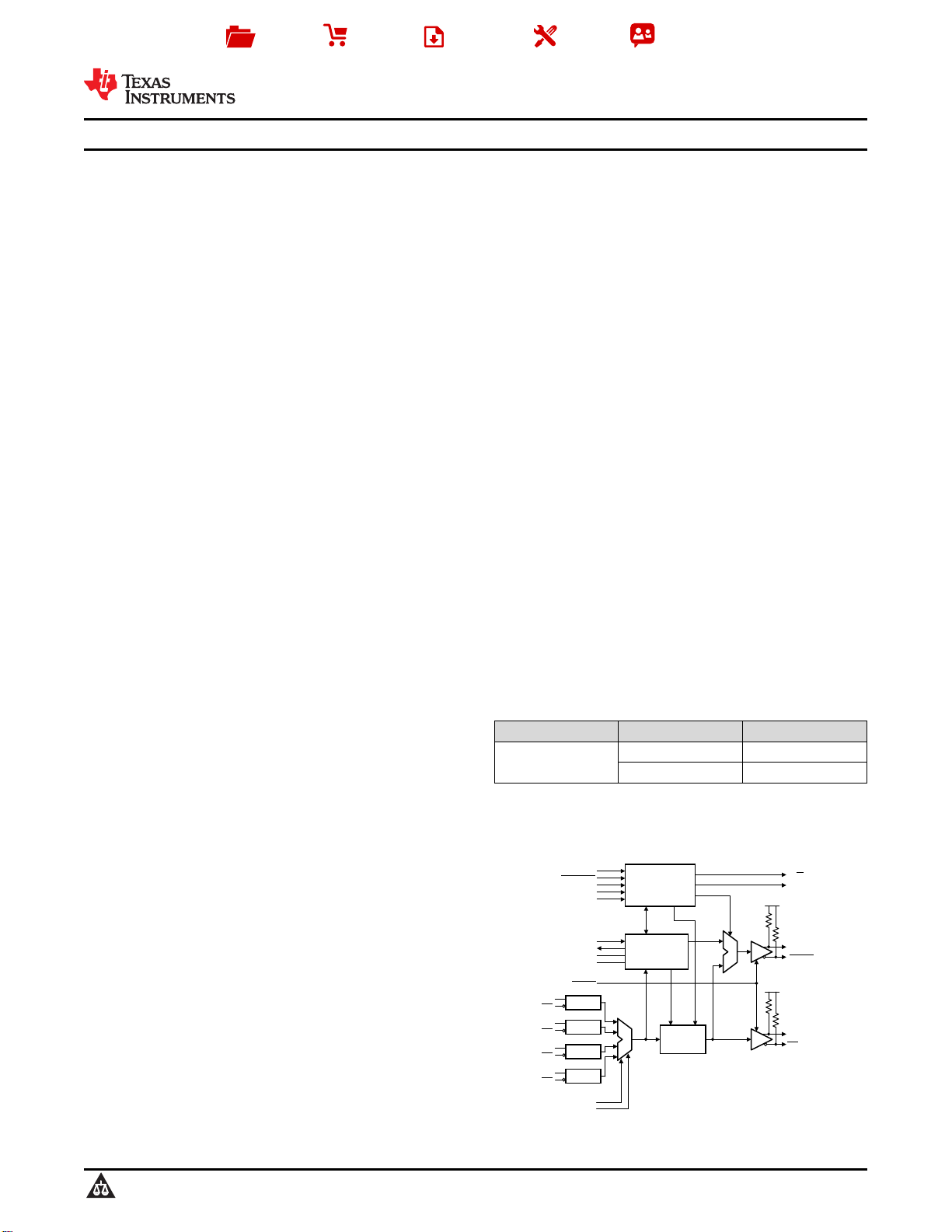
RETIMER / FIFO
VCO / PLL
SDI0
LOCK DETECT
SDO
CONTROL LOGIC
AUTO BYPASS
BYPASS/
O/P MUTE
RATE0
RATE1
50
50
XTAL IN/EXT CLK
XTAL OUT
LOOP FILTER 1
LOOP FILTER 2
SCO_EN
SCO/SDO2
BYPASS
SDI0
SDO
50
50
V
CCO
SD/
HD
V
CCO
SCO/SDO2
SDI1
SDI1
SDI2
SDI2
SDI3
SDI3
SEL0
SEL1
ENABLE
EQUALIZER
EQUALIZER
EQUALIZER
EQUALIZER
Product
Folder
Sample &
Buy
Technical
Documents
Tools &
Software
Support &
Community
SNLS270L –AUGUST 2007–REVISED JANUARY 2016
LMH0356 3-Gbps HD/SD SDI Reclocker with 4:1 Input Mux and FR4 EQs
LMH0356
1 Features
1
• Supports SMPTE ST-424, ST-292, and ST-259
Serial Digital Video Standards
• Supports 270-Mbps, 1.483-Gbps, 1.485-Gbps,
2.967-Gbps, and 2.97-Gbps Serial Data Rate
Operation
• Supports DVB-ASI at 270 Mbps
• Single 3.3-V Supply Operation
• 430-mW Typical Power Consumption
• Integrated 4:1 Multiplexed Input
• 0 to 30-inch FR4 Equalizer on Each Multiplexed
Input
• Two Differential, Reclocked Outputs
• Choice of Second Reclocked Output or
Recovered Clock Output
• Single 27-MHz External Crystal or Reference
Clock Input
• Manual Rate Select Input
• SD/HD Operating Rate Indicator Output
• Lock Detect Indicator Output
• Output Mute Function for Data and Clock
• Auto/Manual Reclocker Bypass
• Power Saver Mode With Device Power-Down
Control (10-mW Typical Power Consumption in
Disabled State)
• Differential LVPECL-Compatible Serial Data
Inputs and Outputs
• LVCMOS Control Inputs and Indicator Outputs
• 48-Pin WQFN or 40-Pin WQFN Package
• Industrial Temperature Range: –40°C to 85°C
• 48-Pin WQFN Version Footprint-Compatible with
the LMH0056 and LMH0036
3 Description
The LMH0356 3-Gbps HD/SD SDI Reclocker with 4:1
Input Mux and FR4 EQs retimes serial digital video
data conforming to the SMPTE ST-424, ST-292, and
ST-259 standards. The LMH0356 operates at serial
data rates of 270 Mbps, 1.483 Gbps, 1.485 Gbps,
2.967 Gbps, and 2.97 Gbps. The LMH0356 supports
DVB-ASI operation at 270 Mbps. The LMH0356
includes an integrated 4:1 input multiplexer for
selecting one of four input data streams for retiming.
In addition, the four inputs of the LMH0356 each have
an FR4 equalizer capable of equalizing 0 to 30 inches
of FR4 trace length.
The LMH0356 automatically detects the incoming
data rate and adjusts itself to retime the incoming
data to suppress accumulated jitter. The LMH0356
recovers the serial data-rate clock and optionally
provides it as an output. The LMH0356 has two
differential serial data outputs; the second output may
be selected as a low-jitter, data-rate clock output.
Controls and indicators are: serial clock or second
serial data output select, manual rate select input,
SD/HD rate indicator output, lock detect output,
auto/manual data bypass, output mute, and device
enable. The serial data inputs, outputs, and serial
clock outputs are differential LVPECL compatible.
The CML serial data and serial clock outputs are
suitable for driving 100-Ω differentially terminated
networks. The control logic inputs and outputs are
LVCMOS compatible.
Device Information
PART NUMBER PACKAGE BODY SIZE (NOM)
LMH0356
(1) For all available packages, see the orderable addendum at
the end of the data sheet.
WQFN (40) 5.00 mm x 5.00 mm
WQFN (48) 7.00 mm x 7.00 mm
(1)
Functional Block Diagram
2 Applications
• SDTV/HDTV and 3-Gbps Serial Digital Video
Interfaces for:
– Digital Video Routers and Switchers
– Digital Video Processing and Editing
Equipment
– DVB-ASI Equipment
– Video Standards and Format Converters
1
An IMPORTANT NOTICE at the end of this data sheet addresses availability, warranty, changes, use in safety-critical applications,
intellectual property matters and other important disclaimers. PRODUCTION DATA.

LMH0356
SNLS270L –AUGUST 2007–REVISED JANUARY 2016
www.ti.com
Table of Contents
1 Features.................................................................. 1
2 Applications ........................................................... 1
3 Description ............................................................. 1
4 Revision History..................................................... 2
5 Description (continued)......................................... 3
6 Pin Configuration and Functions......................... 3
7 Specifications......................................................... 6
7.1 Absolute Maximum Ratings ..................................... 6
7.2 ESD Ratings.............................................................. 6
7.3 Recommended Operating Conditions....................... 6
7.4 Thermal Information.................................................. 6
7.5 DC Electrical Characteristics .................................... 7
7.6 AC Electrical Characteristics..................................... 8
7.7 AC Timing Requirements.......................................... 9
8 Detailed Description............................................ 10
8.1 Overview ................................................................. 10
8.2 Functional Block Diagram....................................... 10
8.3 Feature Description................................................. 11
8.4 Device Functional Modes ....................................... 14
9 Application and Implementation ........................ 15
9.1 Application Information............................................ 15
9.2 Typical Application ................................................. 15
10 Power Supply Recommendations ..................... 19
11 Layout................................................................... 20
11.1 Layout Guidelines ................................................. 20
11.2 Layout Example .................................................... 20
12 Device and Documentation Support................. 21
12.1 Community Resources.......................................... 21
12.2 Trademarks........................................................... 21
12.3 Electrostatic Discharge Caution............................ 21
12.4 Glossary................................................................ 21
13 Mechanical, Packaging, and Orderable
Information........................................................... 21
4 Revision History
NOTE: Page numbers for previous revisions may differ from page numbers in the current version.
Changes from Revision K (April 2013) to Revision L Page
• Added ESD Ratings table, Thermal Information table, Feature Description section, Device Functional Modes
section, Application and Implementation section, Power Supply Recommendations section, Layout section, Device
and Documentation Support section, and Mechanical, Packaging, and Orderable Information section. ............................. 1
2
Submit Documentation Feedback Copyright © 2007–2016, Texas Instruments Incorporated
Product Folder Links: LMH0356
1
LMH0356SQ
(top view)
V
CC
SDI0
SDI0
SCO/SDO2
SCO/SDO2
V
CC
XTAL IN/
EXT CLK
V
EE
V
CC
SDI1
SDI1
ENABLE
SDI2
SDI2
SDI3
SDI3
2
3
4
5
6
7
8
9
10
11
12
13 14 15 16 17 18 19 20 21 22 23 24
36
35
34
33
32
31
30
29
28
27
26
25
48 47 46 45 44 43 42 41 40 39 38 37
SDO
SDO
V
EE
V
CC
BYPASS/
V
EE
LF1
SEL1
SEL0
LF2
V
EE
SCO_EN
V
EE
V
CC
V
CC
V
EE
V
EE
V
CC
V
CC
OP MUTE
XTAL OUT
VEEV
EE
V
EE
V
EE
SD/HD
RATE1
RATE0
V
EE
V
EE
V
EE
AUTO BP
LMH0356
www.ti.com
SNLS270L –AUGUST 2007–REVISED JANUARY 2016
5 Description (continued)
The LMH0356 is powered from a single 3.3-V supply. Power dissipation is typically 430 mW. The device is
available in two space-saving packages: a 7-mm x 7-mm, 48-pin WQFN and even more space-efficient
5-mm x 5-mm, 40-pin WQFN package.
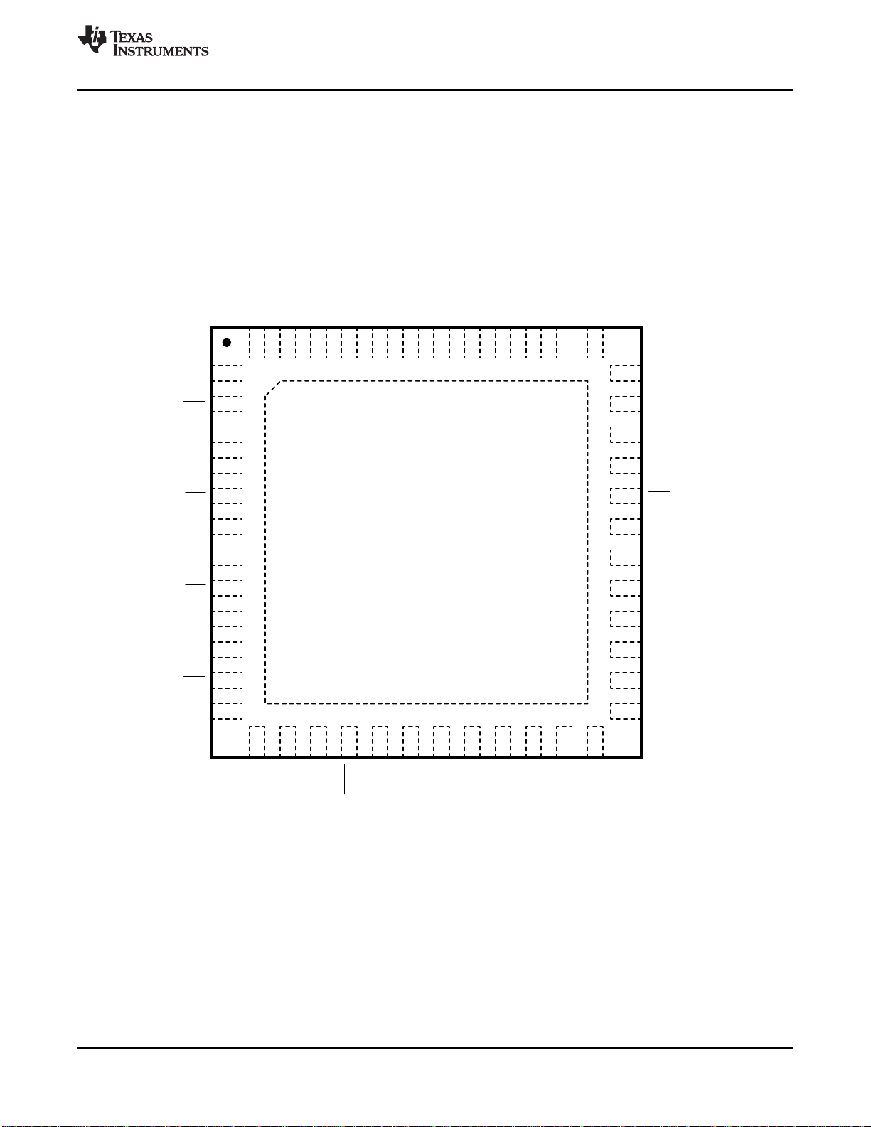
6 Pin Configuration and Functions
RHS Package
48-Pin WQFN
Top View
The exposed die attach pad is the primary negative electrical terminal for this device. It must be connected to the
negative power supply voltage.
Product Folder Links: LMH0356
Submit Documentation FeedbackCopyright © 2007–2016, Texas Instruments Incorporated
3
1
LMH0356SQ-40
(top view)
V
CC
SDI0
SDI0
SCO/SDO2
SCO/SDO2
XTAL IN/
EXT CLK
SDI1
SDI1
ENABLE
SDI2
SDI2
SDI3
SDI3
2
3
4
5
6
7
8
9
10
11 12 13 14 15 16 17 18 19 20
30
29
28
27
26
25
24
23
22
21
40 39 38 37 36 35 34 33 32 31
SDO
SDO
NC
V
CC
BYPASS/
V
CC
LF1
SEL1
SEL0
LF2
SCO_EN
V
EE
V
CC
V
CC
OP MUTE
V
EE
V
EE
LOCK DET
V
EE
SD/HD
RATE1
RATE0
V
EE
V
EE
AUTO BP
V
CC
NC
LMH0356
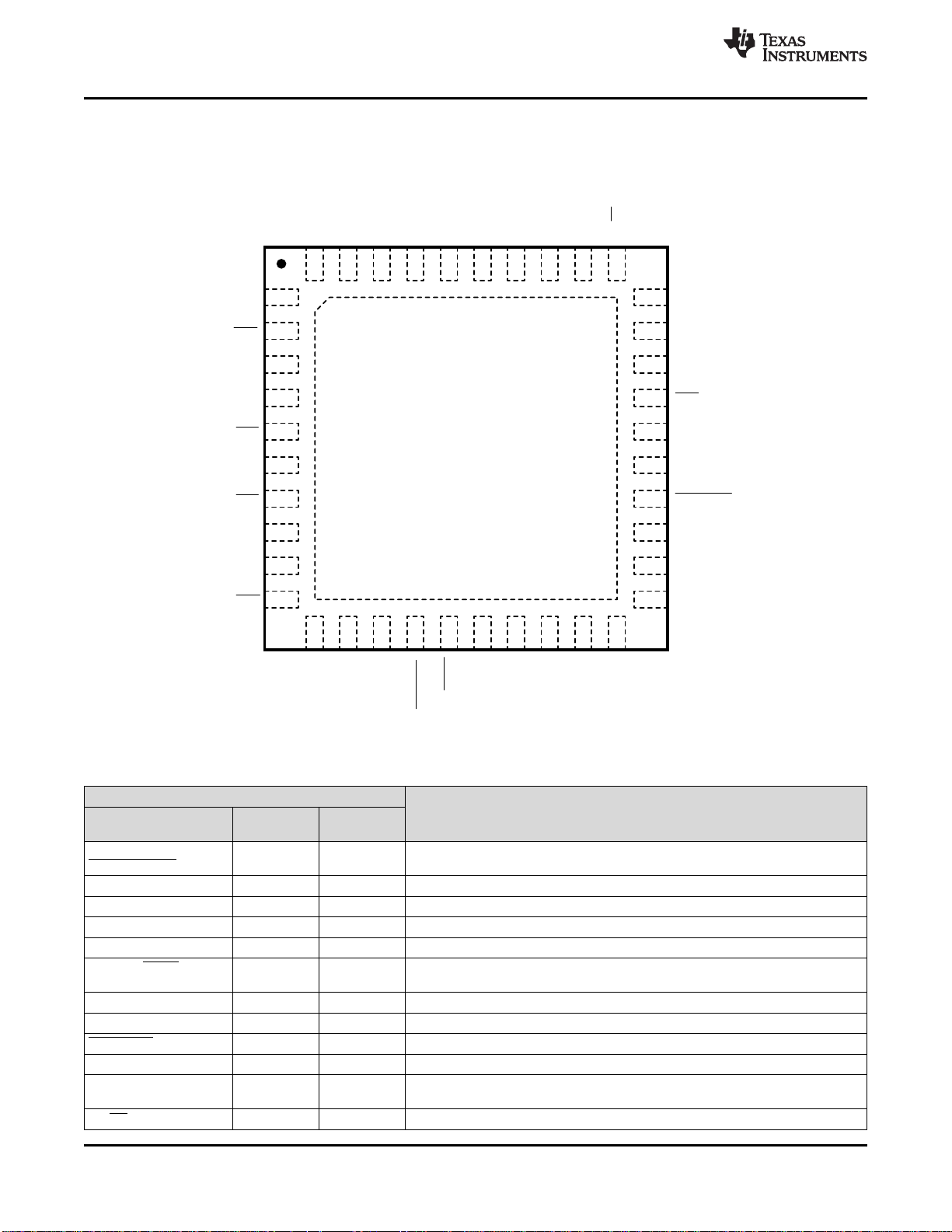
SNLS270L –AUGUST 2007–REVISED JANUARY 2016
www.ti.com
RSB Package
40-Pin WQFN
Top View
The exposed die attach pad is the primary negative electrical terminal for this device. It must be connected to the
negative power supply voltage.
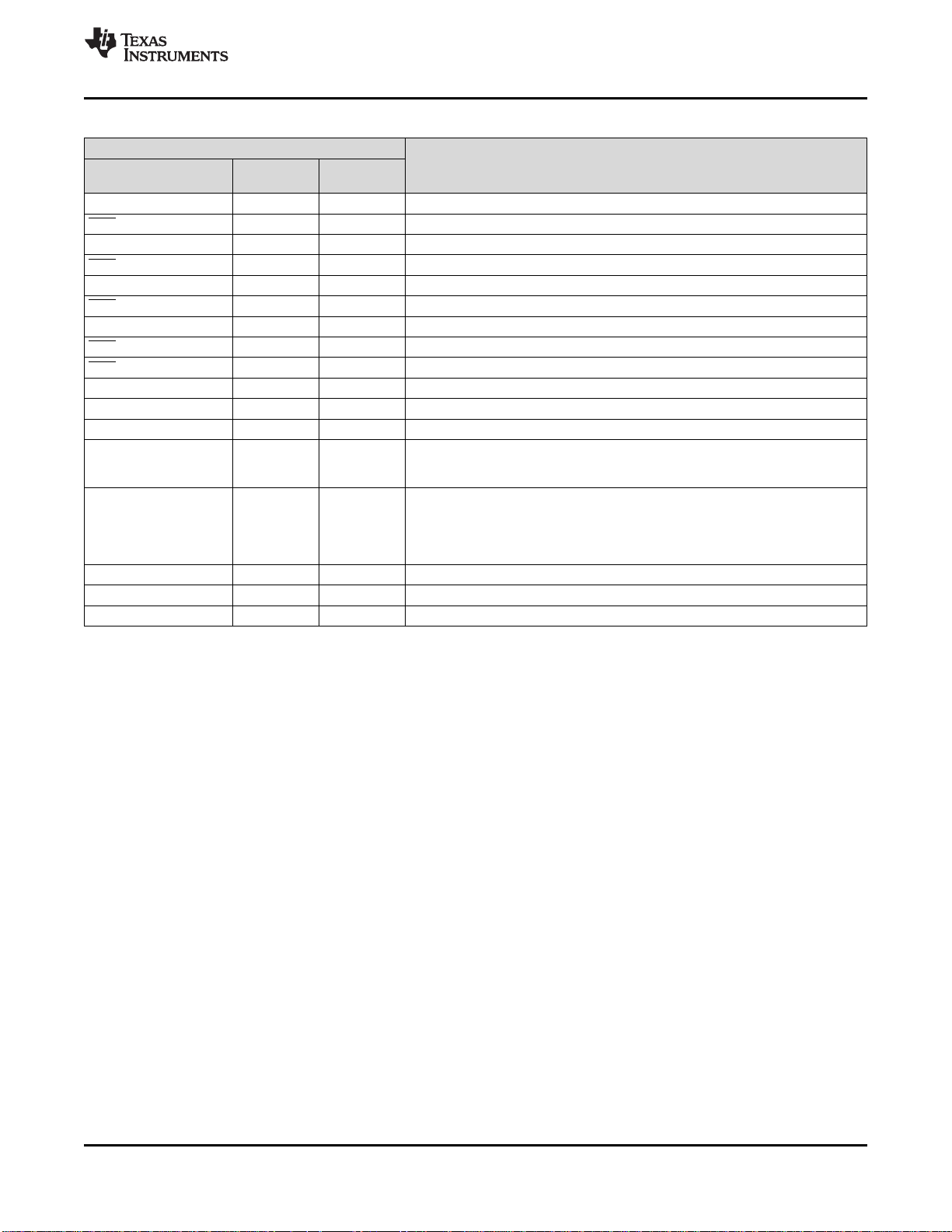
Pin Functions
PIN
NAME
BYPASS/
AUTO BYPASS
ENABLE 9 8 Device Enable. Powers down device when low. This pin has an internal pullup.
LF1 43 35 Loop Filter.
LF2 44 36 Loop Filter.
LOCK DETECT 24 23 PLL Lock Detect output (active high).
OUTPUT MUTE 16 15 Data and Clock Output Mute input. Mutes the output when low. This pin has an
WQFN
48 PIN
15 14 Bypass/Auto Bypass mode select. Bypasses reclocking when high. This pin has
WQFN
40 PIN
an internal pulldown.
internal pullup.
DESCRIPTION
RATE0 45 37 Data Rate select input. This pin has an internal pulldown.
RATE1 46 38 Data Rate select input. This pin has an internal pulldown.
SCO/SDO2 28 24 Serial Clock or Serial Data Output 2 Complement.
SCO/SDO2 29 25 Serial Clock or Serial Data Output 2 True.
SCO_EN 37 32 Serial Clock or Serial Data 2 Output select. Sets second output to output the
clock when high and the data when low. This pin has an internal pulldown.
SD/HD 36 31 Data Rate Range output. Output is high for SD and low for HD or 3G.
4
Submit Documentation Feedback Copyright © 2007–2016, Texas Instruments Incorporated
Product Folder Links: LMH0356
www.ti.com
SNLS270L –AUGUST 2007–REVISED JANUARY 2016
Pin Functions (continued)
PIN
NAME
WQFN
48 PIN
WQFN
40 PIN
SDI0 1 1 Data Input 0 True.
SDI0 2 2 Data Input 0 Complement.
SDI1 4 4 Data Input 1 True.
SDI1 5 5 Data Input 1 Complement.
SDI2 7 6 Data Input 2 True.
SDI2 8 7 Data Input 2 Complement.
SDI3 10 9 Data Input 3 True.
SDI3 11 10 Data Input 3 Complement.
SDO 32 27 Data Output Complement.
SDO 33 28 Data Output True.
SEL0 47 39 Data Input select input. This pin has an internal pulldown.
SEL1 48 40 Data Input select input. This pin has an internal pulldown.
V
CC
30, 31, 34,
35,
3, 6, 12, 14,
3, 11, 13, 26,
29, 30
Positive power supply input.
DAP, 13, 17,
V
EE
23, 25, 26,
27, 38, 39,
19, 20, 21,
12, 17, 18,
20, 33, 34
Negative power supply input.
40, 41, 42
XTAL IN/EXT CLK 18 16 Crystal or External Oscillator input.
XTAL OUT 22 19 Crystal Oscillator output.
NC — 21, 22 No connect.
DESCRIPTION
LMH0356
Product Folder Links: LMH0356
Submit Documentation FeedbackCopyright © 2007–2016, Texas Instruments Incorporated
5
LMH0356
SNLS270L –AUGUST 2007–REVISED JANUARY 2016
www.ti.com
7 Specifications
7.1 Absolute Maximum Ratings
over operating free-air temperature range (unless otherwise noted)
Supply voltage (VCC– VEE) 4 v
Logic supply voltage VEE– 0.15 VCC+ 0.15 V
Logic input current (single input)
Vi = VEE– 0.15 V –5
Vi = VCC+ 0.15 V 5
Logic output voltage VEE– 0.15 VCC+ 0.15 V
Logic output source/sink current –8 8 mA
Serial data output sink current 24 mA
Junction temperature (TJ) 125 °C
Storage temperature (T
) –65 150 °C
stg
(1) Stresses beyond those listed under Absolute Maximum Ratings may cause permanent damage to the device. These are stress ratings
only, which do not imply functional operation of the device at these or any other conditions beyond those indicated under Recommended
Operating Conditions. Exposure to absolute-maximum-rated conditions for extended periods may affect device reliability.
7.2 ESD Ratings
Human-body model (HBM), per ANSI/ESDA/JEDEC JS-001
V
(ESD)
Electrostatic discharge
(1) JEDEC document JEP155 states that 500-V HBM allows safe manufacturing with a standard ESD control process. Manufacturing with
less than 500-V HBM is possible with the necessary precautions. Pins listed as ±8000 V may actually have higher performance.
(2) JEDEC document JEP157 states that 250-V CDM allows safe manufacturing with a standard ESD control process. Manufacturing with
less than 250-V CDM is possible with the necessary precautions. Pins listed as ±1250 V may actually have higher performance.
Charged-device model (CDM), per JEDEC specification JESD22-
(2)
C101
Machine model (MM) ±400
(1)
MIN MAX UNIT
mA
VALUE UNIT
(1)
±8000
±1250
V
7.3 Recommended Operating Conditions
over operating free-air temperature range (unless otherwise noted)
MIN NOM MAX UNIT
Supply voltage 3.3 – 5% 3.3 + 5% V
Logic input voltage V
EE
Differential serial input voltage 800 – 10% 800 + 10% mV
Serial data or clock output sink current 16 mA
Operating free-air temperature –40 85 °C
V
CC
V
7.4 Thermal Information
LMH0356
THERMAL METRIC
R
θJA
R
θJC(top)
R
θJC(bot)
Junction-to-ambient thermal resistance 28.3 31.2 °C/W
Junction-to-case (top) thermal resistance 8.8 16.8 °C/W
Junction-to-case (bottom) thermal resistance 1.3 1.2 °C/W
(1) For more information about traditional and new thermal metrics, see the Semiconductor and IC Package Thermal Metrics application
report (SPRA953).
(1)
UNITRHS (WQFN) RSB (WQFN)
48 PINS 40 PINS
6
Submit Documentation Feedback Copyright © 2007–2016, Texas Instruments Incorporated
Product Folder Links: LMH0356
LMH0356
www.ti.com
SNLS270L –AUGUST 2007–REVISED JANUARY 2016
7.5 DC Electrical Characteristics
over supply voltage and recommended operating temperature ranges (unless otherwise noted)
PARAMETER TEST CONDITIONS MIN TYP MAX UNIT
V
IH
V
IL
I
IH
I
IL
V
OH
V
OL
V
SDID
V
CMI
V
SDOD
V
SCOD
V
CMO
I
CC
(1) Current flow into device pins is defined as positive. Current flow out of device pins is defined as negative. All voltages are referenced to
(2) Typical values are stated for: VCC= 3.3 V, TA= 25°C.
(3) This parameter is ensured by characterization over voltage and temperature limits.
Logic input voltage high level 2 V
Logic input voltage low level V
Logic input current high level VIH= V
Logic input current low level VIL= V
CC
EE
EE
Logic output voltage high level IOH= −2 mA 2 V
Logic output voltage low level IOL= 2 mA VEE+ 0.6 V
Serial input voltage, differential SDI
Input common mode voltage V
Serial data output voltage,
differential
Serial clock output voltage,
differential
(3)
SDID
= 200 mV
(3)
SDO, SDO2 100-Ω differential
load
SCO 100-Ω differential load,
2970 MHz
(3)
SCO 100-Ω differential load,
200 1600 mV
VEE+ 0.95 VCC− 0.2 V
620 750 880 mV
400 525 650 mV
1485 or 270 MHz
Output common mode voltage
Power supply current, 3.3-V
supply, total
SDO, SCO 100-Ω differential
load
VCC− V
2970 Mbps, device enabled 130 150 mA
Device disabled
(ENABLE = 0)
VEE(equal to zero volts).
(1)(2)
CC
0.8 V
47 65 µA
−18 −25 µA
750 mV
SDOD
3 mA
V
P-P
P-P
P-P
P-P
V
Product Folder Links: LMH0356
Submit Documentation FeedbackCopyright © 2007–2016, Texas Instruments Incorporated
7
LMH0356
SNLS270L –AUGUST 2007–REVISED JANUARY 2016
www.ti.com
7.6 AC Electrical Characteristics
over supply voltage and recommended operating temperature ranges (unless otherwise noted)
PARAMETER TEST CONDITIONS MIN TYP MAX UNIT
BR
SD
BR
SD
BR
SD
TOL
JIT
TOL
JIT
TOL
JIT
TOL
JIT
TOL
JIT
TOL
JIT
t
JIT
t
JIT
t
JIT
BW
LOOP
F
CO
F
CO
F
CO
F
CO
F
CO
t
JIT
SC
ALG
SC
ODC
F
REF
F
TOL
(1) Typical values are stated for: VCC= 3.3 V, TA= 25°C.
(2) Peak-to-peak amplitude with sinusoidal modulation per SMPTE RP 184-1996 paragraph 4.1. The test data signal shall be color bars.
(3) This parameter is ensured by characterization over voltage and temperature limits.
(4) Refer to A1 in Figure 1 of SMPTE RP 184-1996.
(5) Refer to A2 in Figure 1 of SMPTE RP 184-1996.
(6) PRBS 210– 1, input jitter = 31 ps
(7) PRBS 210– 1, input jitter = 24 ps
(8) PRBS 210– 1, input jitter = 22 ps
Serial data rate ST-259 270 Mbps
Serial data rate ST-292 1483, 1485 Mbps
Serial data rate ST-424 2967, 2970 Mbps
Serial input jitter tolerance 270 Mbps
Serial input jitter tolerance 270 Mbps
Serial input jitter tolerance 1483 or 1485 Mbps
Serial input jitter tolerance 1483 or 1485 Mbps
Serial input jitter tolerance 2967 or 2970 Mbps
Serial input jitter tolerance 2967 or 2970 Mbps
(2) (3) (5)
Serial data output jitter 270 Mbps
Serial data output jitter 1483 or 1485 Mbps
Serial data output jitter 2967 or 2970 Mbps
(2)(3)(4)
(2)(3)(5)
(3)(6)
(2)(3)(4)
(2)(3)(5)
(2)(3)(4)
(3)(7)
(3)(8)
>6 UI
>0.6 UI
>6 UI
>0.6 UI
>6 UI
>0.6 UI
270-Mbps,
<0.1-dB Peaking
Loop bandwidth
1485-Mbps,
<0.1-dB Peaking
2970 Mbps,
<0.1-dB Peaking
Serial clock output
270-Mbps data rate
frequency
Serial clock output
1483-Mbps data rate
frequency
Serial clock output
1485-Mbps data rate
frequency
Serial clock output
2967-Mbps data rate
frequency
Serial clock output
2970-Mbps data rate
frequency
Serial Clock Output Jitter 2 3 ps
Serial clock output
alignment with respect to
See
(3)
40% 60%
data interval
Serial clock output duty
cycle
See
(3)
45% 55%
Reference clock
frequency
Reference clock
frequency tolerance
.
P-P
.
P-P
.
P-P
(1)
P-P
P-P
P-P
P-P
P-P
P-P
0.01 0.03 UI
0.04 0.05 UI
0.08 0.09 UI
P-P
P-P
P-P
275 kHz
1.5 MHz
2.75 MHz
270 MHz
1483 MHz
1485 MHz
2967 MHz
2970 MHz
RMS
27 MHz
±50 ppm
8
Submit Documentation Feedback Copyright © 2007–2016, Texas Instruments Incorporated
Product Folder Links: LMH0356
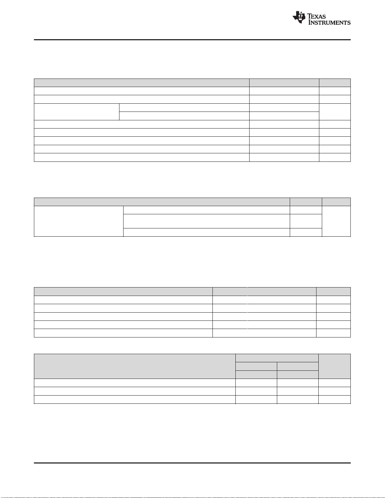
SDI 270 MBPS DATANO DATA
T
2
1485 MBPS DATA 2970 MBPS DATA 270 MBPS DATA
T
1
T
ACQ
T
2
T
2
SDI 270 MBPS DATANO DATA
Lock
Dete
ct
SD/HD
T
2
NO DATA 1485 MBPS DATA NO DATA
T
2
Lock
Dete
ct
SD/HD
T
1
T
ACQ
T
1
T
ACQ
T
ACQ
T
1
T
ACQ
T
1
T
1
T
ACQ
T
1
T
1
www.ti.com
7.7 AC Timing Requirements
T
tr, t
tr, t
tr, t
tr, t
tr, t
tr, t
ACQ
f
f
f
f
f
f
Acquisition time See
Logic inputs rise/fall time 10%–90% 1.5 ns
Input rise/fall time 20%–80%, 270 Mbps
Input rise/fall time 20%–80%, 1483 or 1485 Mbps
Input rise/fall time 20%–80%, 2967 or 2970 Mbps
Logic outputs rise/fall time 10%–90% 1.5 ns
Output rise/fall time 20%–80%
(1) Measured from first SDI transition until Lock Detect output goes high (true).
(2) This specification is ensured by design.
(3) RL= 100-Ω differential.
(4) This parameter is ensured by characterization over voltage and temperature limits.
(1)
(2)
(2)
(2)
(3) (4)
LMH0356
SNLS270L –AUGUST 2007–REVISED JANUARY 2016
MIN NOM MAX UNIT
15 ms
1500 ps
270 ps
135 ps
90 130 ps
T
= Acquisition Time, defined in AC Timing Requirements
ACQ
T1= Time from Lock Detect assertion or deassertion until SD/HD output is valid, typically 37 ns (one 27-MHz clock
period)
T2= Time from SDI input change until Lock Detect deassertion, 1 ms maximum. SD/HD output is not valid during this
time.
Figure 1. SDI, Lock Detect, and SD/HD Timing
Submit Documentation FeedbackCopyright © 2007–2016, Texas Instruments Incorporated
Product Folder Links: LMH0356
9
RETIMER / FIFO
VCO / PLL
SDI0
LOCK DETECT
SDO
CONTROL LOGIC
AUTO BYPASS
BYPASS/
O/P MUTE
RATE0
RATE1
50
50
XTAL IN/EXT CLK
XTAL OUT
LOOP FILTER 1
LOOP FILTER 2
SCO_EN
SCO/SDO2
BYPASS
SDI0
SDO
50
50
V
CCO
SD/
HD
V
CCO
SCO/SDO2
SDI1
SDI1
SDI2
SDI2
SDI3
SDI3
SEL0
SEL1
ENABLE
EQUALIZER
EQUALIZER
EQUALIZER
EQUALIZER
LMH0356
SNLS270L –AUGUST 2007–REVISED JANUARY 2016
www.ti.com
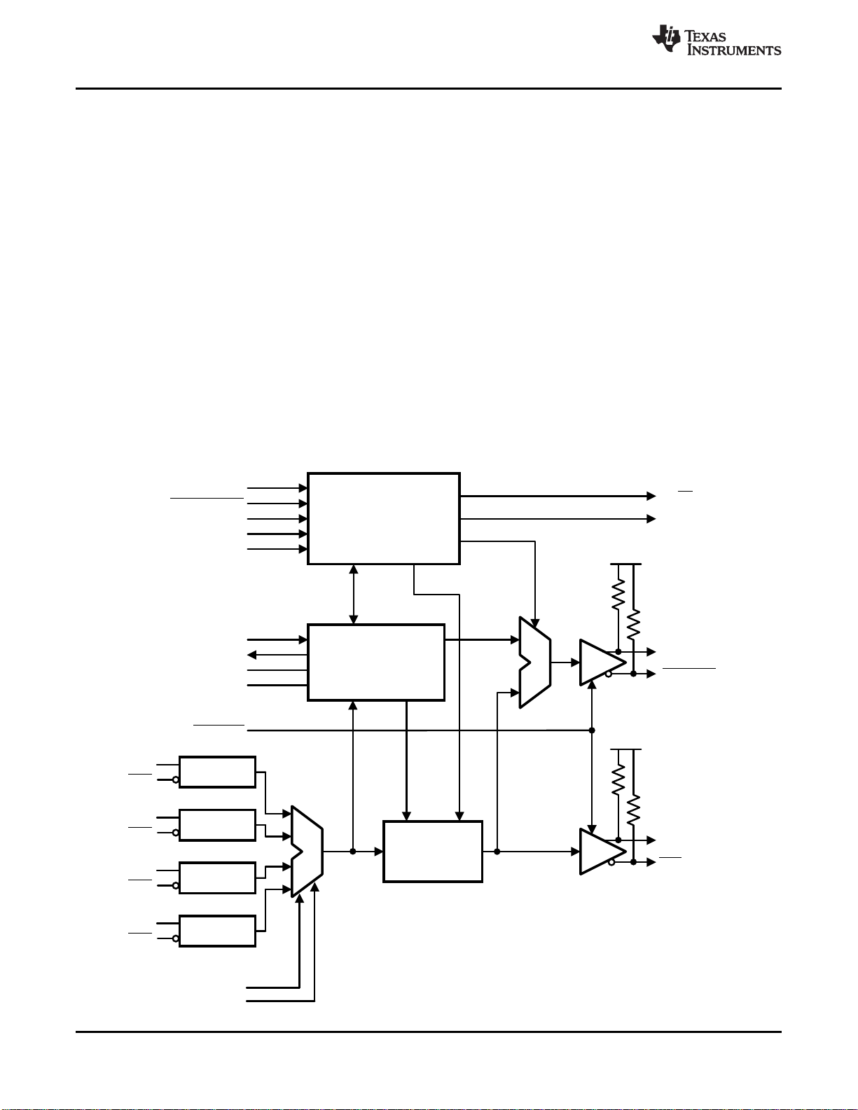
8 Detailed Description
8.1 Overview
The LMH0356 3-Gbps HD/SD SDI Reclocker with 4:1 Input Mux and FR4 EQs is used in many types of digital
video signal processing equipment. Supported serial digital video standards are ST-259, ST-292, and ST-424.
Corresponding serial data rates are 270 Mbps, 1.483 Gbps, 1.485 Gbps, 2.967 Gbps, and 2.97 Gbps. DVB-ASI
data at 270 Mbps may also be retimed. The LMH0356 retimes the serial data stream to suppress accumulated
jitter. It provides two low-jitter, differential, serial data outputs. The second output may be selected to output
either serial data or a low-jitter serial data-rate clock. Controls and indicators are: serial clock or second serial
data output select, manual rate select input, SD/HD rate output, lock detect output, auto/manual data bypass and
output mute.
Serial data inputs are CML and LVPECL compatible. Serial data and clock outputs are differential CML and
produce LVPECL compatible levels. The output buffer design can drive AC or DC-coupled, terminated 100-Ω
differential loads. The differential output level is 750 mV
inputs and outputs are LVCMOS compatible.
The device package is a 48-pin WQFN or a 40-pin WQFN. Both package options have an exposed die attach
pad. The exposed die attach pad is electrically connected to device ground (VEE) and is the primary electrical
terminal for the device. This terminal must be connected to the negative power supply or circuit ground.
8.2 Functional Block Diagram
into 100-Ω AC- or DC-coupled differential loads. Logic
P-P
10
Submit Documentation Feedback Copyright © 2007–2016, Texas Instruments Incorporated
Product Folder Links: LMH0356

SDI[3:0]
V
CC
V
CC
SDI[3:0]
2 kW
80 kW
1 pF
20 kW
V
CC
2 kW
50
network
W 50
network
W
LMH0356
www.ti.com
SNLS270L –AUGUST 2007–REVISED JANUARY 2016
8.3 Feature Description
8.3.1 Functional Block Description
8.3.1.1 Serial Data Input and Outputs
The differential serial data inputs, SDI0-SDI3, accept serial digital video data at the rates specified in Table 1.
Figure 2 shows the equivalent input circuit for SDI[3:0] and SDI[3:0]. The serial data inputs are differential
LVPECL compatible. These inputs have 50-Ω internal terminations (100-Ω differential) with an internal bias as
shown in Figure 2. These inputs are intended to be DC-coupled to devices such as the LMH0344 adaptive cable
equalizer. DC-coupled inputs must be kept within the specified common mode range. The inputs may be ACcoupled if the input signal is outside the input common mode range of the device (such as when interfacing to 5V PECL), and in that case the bias is supplied internally so no additional input biasing is required. See Figure 2
for more information on input interfacing.
The LMH0356 provides four independent, equalized and multiplexed data inputs. The active input channel is
selected via the SEL0 and SEL1 pins, as shown in Table 2. The equalizer on each of the four inputs is capable
of equalizing up to 30 inches of FR4 trace without the need for programming for different trace lengths or data
rates.
The LMH0356 has two retimed, differential, serial data outputs: SDO and SCO/SDO2. These outputs provide
low-jitter, differential, retimed data to devices such as the LMH0302 cable driver. Output SCO/SDO2 is
multiplexed and can provide either a second serial data output or a serial clock output. Figure 3 shows the
equivalent output circuit for SDO, SDO, SCO/SDO2, and SCO/SDO2.
The SCO_EN input controls the operating mode for the SCO/SDO2 output. When the SCO_EN input is high the
SCO/SDO2 output provides a serial clock. When SCO_EN is low, the SCO/SDO2 output provides retimed serial
data.
Both differential serial data outputs, SDO and SCO/SDO2, are muted when the OUTPUT MUTE input is a logic
low level. SCO/SDO2 also mutes when the Bypass mode is activated when this output is operating as the serial
clock output. When muted, SDO and SDO (or SDO2 and SDO2) will assume opposite differential output levels.
The CML serial data outputs are differential LVPECL compatible. These outputs have internal 50-Ω pullups and
are suitable for driving AC- or DC-coupled, 100-Ω center-tapped, AC-grounded or 100-Ω un-center-tapped,
differentially terminated networks.
Figure 2. Equivalent SDI Input Circuit (SDI[3:0], SDI[3:0])
Product Folder Links: LMH0356
Submit Documentation FeedbackCopyright © 2007–2016, Texas Instruments Incorporated
11

50:
SDO, SCO/SDO2
V
CC
V
CC
50:
V
CC
SDO, SCO/SDO2
LMH0356
SNLS270L –AUGUST 2007–REVISED JANUARY 2016
www.ti.com
Feature Description (continued)
Figure 3. Equivalent SDO Output Circuit (SDO, SDO, SCO/SDO2, SCO/SDO2)
8.3.1.2 Operating Serial Data Rates
This device operates at serial data rates of 270 Mbps, 1483 Mbps, 1485 Mbps, 2967 Mbps, and 2970 Mbps. The
device does not lock to harmonics of these rates. The device does not lock and automatically enters the
reclocker bypass mode for the following data rates: 143 Mbps, 177 Mbps, 360 Mbps, and 540 Mbps.
8.3.1.3 Serial Data Clock/Serial Data 2 Output
The Serial Data Clock/Serial Data 2 Output is controlled by the SCO_EN input and provides either a second
retimed serial data output or a low jitter differential clock output appropriate to the serial data rate being
processed. When operating as a serial clock output, the rising edge of the clock is positioned within the
corresponding serial data bit interval within 10% of the center of the data interval.
Differential output SCO/SDO2 functions as the second serial data output when the SCO_EN input is a logic-low
level. This output functions as the serial clock output when the SCO_EN input is a logic-high level. The SCO_EN
input has an internal pulldown device and the default state of SCO_EN is low (serial data output 2 enabled).
SCO/SDO2 is muted when the OUTPUT MUTE input is a logic low level. When the Bypass mode is activated
and this output is functioning as a serial clock output, the output is muted. If an unsupported data rate is used
while in Auto Bypass mode with this output functioning as a serial clock output, the output is invalid.
8.3.2 Control Inputs and Indicator Outputs
8.3.2.1 Serial Data Rate Selector
The Serial Data Rate Selector (RATE [1:0]) permits the user to fix the operating serial data rate. RATE[1:0] pins
have internal pull-downs which maintain a logic-low input condition unless externally driven to a logic-high
condition. This input also serves to place the device in a test mode. The codes shown in Table 1 select the
desired operating serial data rate. The LMH0356 then enters either the Auto-Rate Detect mode or a single
operating rate. Selecting the 270-Mbps rate mode may also be used when reclocking DVB-ASI data. DVB-ASI
data is MPEG2 coded data that is transmitted in 8B10B coding. The device reclocks this data without harmonic
locking.
RATE [1:0]
CODE
00 Auto-Rate Detect mode
01 270 Mbps May be used to support DVB-ASI operation
10 1483/1485 Mbps, 2967/2970 Mbps
Table 1. Data Rate Select Input Codes
DATA RATE OR MODE COMMENTS
12
Submit Documentation Feedback Copyright © 2007–2016, Texas Instruments Incorporated
Product Folder Links: LMH0356

LMH0356
www.ti.com
SNLS270L –AUGUST 2007–REVISED JANUARY 2016
8.3.2.2 Serial Data Input Selector
The Serial Data Input Selector (SEL [1:0]) allows the user to select the active input channel. Table 2 shows the
input selected for a given state of SEL [1:0]. The SEL pins have internal pulldowns.
Table 2. Data Input Select Codes
SEL [1:0] CODE SELECTED INPUT
00 SDI0
01 SDI1
10 SDI2
11 SDI3
8.3.2.3 Lock Detect
The Lock Detect output, when high, indicates that data is being received and the PLL is locked. Lock Detect may
be connected to the OUTPUT MUTE input to mute the data and clock outputs when no data signal is being
received. Note that when the Bypass/Auto Bypass input is set high, Lock Detect will remain low. See Table 3.
8.3.2.4 OUTPUT MUTE
The OUTPUT MUTE input, when low, mutes the serial data and clock outputs. It may be connected to Lock
Detect or externally driven to mute or un-mute the outputs. If OUTPUT MUTE is connected to Lock Detect, then
the data and clock outputs are muted when the PLL is not locked. This function overrides the Bypass function;
see Table 3. OUTPUT MUTE has an internal pullup device to enable the output by default.
8.3.2.5 Bypass/AUTO BYPASS
The Bypass/Auto Bypass input, when high, forces the device to output the data without reclocking it. When this
input is low, the device automatically bypasses the reclocking function when the device is in an unlocked
condition or the detected data rate is a rate which the device does not support. Note that when the Bypass/Auto
Bypass input is set high, Lock Detect remains low. See Table 3. BYPASS/AUTO BYPASS has an internal
pulldown device.
Table 3. Control Functionality
LOCK DETECT OUTPUT MUTE BYPASS/AUTO BYPASS DEVICE STATUS
0 1 X PLL unlocked, reclocker bypassed
1 1 0 PLL locked to supported data rate, reclocker not bypassed
X 0 X Outputs muted
0 LOCK DETECT X Outputs muted
1 LOCK DETECT 0 PLL locked to supported data rate, reclocker not bypassed
8.3.2.6 SD/HD
The SD/HD output indicates whether the LMH0356 is processing SD or HD / 3 Gbps data rates. It may be used
to control another device such as the LMH0302 cable driver. When this output is high it indicates that the data
rate is 270 Mbps. When low, the indicated data rate is 1483, 1485, 2967, or 2970 Mbps. The SD/HD output is a
registered function and is only valid when the PLL is locked and the Lock Detect output is high. When the PLL is
not locked (the Lock Detect output is low), the SD/HD output defaults to HD (low). The SD/HD output is
undefined for a short time after lock detect assertion or de-assertion due to a data rate change on SDI. See
Figure 1 for a timing diagram showing the relationship between SDI, Lock Detect, and SD/HD.
8.3.2.7 SCO_EN
Input SCO_EN enables the SCO/SDO2 differential output to function either as a serial clock or second serial
data output. SCO/SDO2 functions as a serial clock when SCO_EN is high. This pin has an internal pulldown
device. The default state (low) enables the SCO/SDO2 output as a second serial data output.
Submit Documentation FeedbackCopyright © 2007–2016, Texas Instruments Incorporated
Product Folder Links: LMH0356
13

LMH0356
SNLS270L –AUGUST 2007–REVISED JANUARY 2016
www.ti.com
8.3.2.8 ENABLE
The ENABLE pin is used to enable or disable the LMH0356. When the device is disabled, the output drivers and
most of the internal circuitry are powered down. The crystal oscillator and external clock reference circuitry
(XTAL IN and XTAL OUT) remain active regardless of the state of ENABLE, allowing the 27-MHz reference clock
signal to be generated and passed on to additional reclockers. The ENABLE pin is active high and has an
internal pullup device to enable the LMH0356 by default.
8.3.2.9 Crystal or External Clock Reference
The LMH0356 uses a 27-MHz crystal or external clock signal as a timing reference input. A 27-MHz parallel
resonant crystal and load network may be connected to the XTAL IN/EXT CLK and XTAL OUT pins.
Alternatively, a 27-MHz LVCMOS compatible clock signal may be input to XTAL IN/EXT CLK. Parameters for a
suitable crystal are given in Table 4.
Table 4. Crystal Parameters
PARAMETER VALUE
Frequency 27 MHz
Frequency stability ±50 ppm at recommended drive level
Operating mode Fundamental mode, parallel resonant
Load capacitance 20 pF
Shunt capacitance 7 pF
Series resistance 40 Ω (maximum)
Recommended drive level 100 µW
Maximum drive level 500 µW
Operating temperature −10°C to 60°C
8.4 Device Functional Modes
The LMH0356 features are programmed using pin control. Refer to Control Inputs and Indicator Outputs for
details.
14
Submit Documentation Feedback Copyright © 2007–2016, Texas Instruments Incorporated
Product Folder Links: LMH0356

LMH0344
Equalizer
DS25CP104
4x4 LVDS
Crosspoint
LMH0356
Reclocker
LMH0344
Equalizer
LMH0344
Equalizer
LMH0344
Equalizer
LMH0344
Equalizer
LMH0344
Equalizer
LMH0344
Equalizer
LMH0344
Equalizer
LMH0302
Cable Driver
LMH0302
Cable Driver
0-30" FR4
DS25CP104
4x4 LVDS
Crosspoint
0-20" FR4
LMH0356
www.ti.com
SNLS270L –AUGUST 2007–REVISED JANUARY 2016
9 Application and Implementation
NOTE
Information in the following applications sections is not part of the TI component
specification, and TI does not warrant its accuracy or completeness. TI’s customers are
responsible for determining suitability of components for their purposes. Customers should
validate and test their design implementation to confirm system functionality.
9.1 Application Information
The LMH0356 3-Gbps HD/SD SDI Reclocker with 4:1 Input Mux and FR4 EQs is used in many types of digital
video signal processing equipment.
9.2 Typical Application
Figure 4 and Figure 5 show typical system and application circuits for the 48-pin WQFN version of the LMH0356.
Figure 4. System Block Diagram
Product Folder Links: LMH0356
Submit Documentation FeedbackCopyright © 2007–2016, Texas Instruments Incorporated
15

LMH0356
SDI0
SDI0
1
2
3
4
5
6
7
8
9
10
11
12
SCO_EN
25
26
27
28
29
30
31
32
33
34
SCO/SDO2
SCO/SDO2
SDO
SDO
HD
SD/
131415161718192021
22
V
CC
SDI1
SDI1
V
CC
SDI2
SDI2
SDI3
SDI3
ENABLE
V
EE
V
CC
V
CC
MUTE
XTAL IN/EXT CLK
BP/
AUTO BP
VEEVEEVEEV
EE
XTAL OUT
LOCK DET
23
24
V
EE
V
EE
V
EE
V
EE
35
36
V
CC
V
CC
V
CC
V
CC
37
38
39
40
41
42
43
44
45
46
47
48
DAP
VEEVEEVEEVEEV
EE
SEL1
SEL0
RATE1
RATE0
LF2
LF1
Differential
Data Input 3
V
CC
Differential
Data Input 2
Differential
Data Input 1
Differential
Data Input 0
ENABLE
V
CC
27 MHz
39 pF 39 pF
Data
Output
Clock Output or
2nd Data Output
HD
SD/
V
CC
56 nF
LOCK DET
MUTE
BYPASS/
AUTO BP
SEL1
SEL0
RATE1
RATE0
SCO_EN
OP
OP
LMH0356
SNLS270L –AUGUST 2007–REVISED JANUARY 2016
Typical Application (continued)
www.ti.com
ENABLE has an internal pullup to enable the device by default. This pin may be pulled low to put the LMH0356
into a powered down mode.
BP/AUTO BP has an internal pulldown to enable Auto Bypass mode by default. This pin may be pulled high to
force the LMH0356 to bypass all data.
OP MUTE has an internal pullup to enable the outputs by default. This pin may be pulled low to mute the
outputs.
The XTAL IN/EXT CLK and XTAL OUT pins are shown with a 27-MHz crystal and the proper loading. The crystal
should match the parameters described in Table 4. Alternately, a 27-MHz LVCMOS compatible clock signal may
be input to XTAL IN/EXT CLK.
The active high LOCK DET output provides an indication that proper data is being received and the PLL is
locked.
The SD/HD output may be used to drive the SD/HD pin of an SDI cable driver (such as the LMH0302) in order to
properly set the cable driver’s edge rate for SMPTE compliance. It defaults to HD/3G (low) when the LMH0356 is
not locked.
16
Submit Documentation Feedback Copyright © 2007–2016, Texas Instruments Incorporated
Figure 5. Application Circuit
Product Folder Links: LMH0356

LMH0356
www.ti.com
SNLS270L –AUGUST 2007–REVISED JANUARY 2016
Typical Application (continued)
SCO_EN has an internal pulldown to set the second output (SCO/SDO2) to output data. This pin may be pulled
high to set the second output as a serial clock.
The external loop filter capacitor (between LF1 and LF2) must be 56 nF. This is the only supported value; the
loop filter capacitor must not be changed.
RATE0 and RATE1 have internal pulldowns to select Auto-Rate Detect mode by default. These pins may also be
used to set the device to SD mode or HD/3G mode.
SEL0 and SEL1 have internal pulldowns to select the SDI0 input by default.
9.2.1 Design Requirements
For this design example, use the parameters listed in Table 5 as the input parameters.
Table 5. LMH0356 Design Parameters
DESIGN PARAMETER REQUIREMENTS
Input AC-coupling capacitors
Output AC-coupling capacitors
DC power supply coupling capacitors
High-speed SDI and SDO trace impedance
Use of ENABLE, RATE0/1, SCO_EN, OP MUTE, and
BP/AUTO BP pins
LOCK DET pin
SD/HD Pin Use SD/HD to set cable driver edge rate or to FPGA for lock rate monitoring.
The user should check output common mode voltage of the device attached
to SDI pins. If AC-coupling capacitor is required, AC-coupling capacitor is
expected to be 4.7 μF ±10%. Refer to Input Output Interfacing for details.
The user should check input common mode voltage of the device attached to
SDO pins. If AC-coupling capacitor is required, AC-coupling capacitor is
expected to be 4.7 μF ±10%. Refer to Input Output Interfacing for details.
De-coupling capacitors are required to minimize power supply ripple noise.
Place 4.7-μF and 0.1-μF surface mount ceramic capacitors as close to the
device VCCpin as possible .
SDI± and SDO± must be routed with coupled board traces with 100-Ω ± 5%
differential impedance.
Set these pins for desired operating mode.
Use this pin for lock indication or to OP MUTE pin to enable output when
locked.
9.2.2 Detailed Design Procedure
To begin the design process, determine the following:
1. Check that the power supply meets the DC and AC requirements in DC Electrical Characteristics.
2. Select the proper pull-high or pull-low resistors for ENABLE, RATE0/1, SCO_EN, OP MUTE, and BP/AUTO
BP pins.
3. Use SD/HD output signal to set the cable driver edge rate.
4. Refer to Input Output Interfacing for Input or Output DC- or AC-coupling.
5. Choose small 0402 surface mount ceramic capacitors for AC-coupling and bypass capacitors.
6. Pay close attention to high speed printed circuit board layout for the high speed SDI± and SDO± signals.
7. Plan out overall system jitter budget with AC Electrical Characteristics in mind.
9.2.2.1 Input Output Interfacing
The inputs are LVPECL compatible. The LMH0356 has a wide input common mode range, and in most cases
the input should be DC-coupled. For DC-coupling, the inputs must be kept within the common mode range
specified in DC Electrical Characteristics.
Figure 6 shows an example of a DC-coupled interface between the LMH0344 cable equalizer and the LMH0356.
The LMH0344 output common mode voltage and voltage swing are within the range of the input common mode
voltage and voltage swing of the LMH0356. In this figure, the LMH0344 cable equalizer restores the signal after
the coaxial cable. The LMH0356 FR4 equalizer restores the signal after the loss due to the FR4 trace. The
LMH0356 inputs have 50-Ω internal terminations (100-Ω differential) to terminate the transmission line, so no
additional components are required.
Submit Documentation FeedbackCopyright © 2007–2016, Texas Instruments Incorporated
Product Folder Links: LMH0356
17

LMH0356
100:
SDO
SDO
75:
LMH0302
3G/HD/SD
SDI Cable Driver
SDO
SDI
SDO
SDI
75:
75:
75:
75:
75:
+3.3V
Coaxial Cable
Coaxial Cable
4.7 PF
4.7 PF
5.6 nH
5.6 nH
SD/HDSD/HD
SDO
SDO
0-30" FR4 Trace
LMH0356
SDI0
SDI0
LMH0344
3G/HD/SD
SDI Cable Equalizer
Coaxial Cable
75:
37.4:
75:
3.9 nH
1.0 PF
1.0 PF
SDI
SDI
LMH0356
SNLS270L –AUGUST 2007–REVISED JANUARY 2016
www.ti.com
The outputs are LVPECL compatible. SDO is the primary data output and SCO/SDO2 is a second output that
may be set as the serial clock or a second data output. Both outputs are always active. The LMH0356 output
should be DC-coupled to the input of the receiving device as long as the common mode ranges of both devices
are compatible.
Figure 7 shows an example of a DC-coupled interface between the LMH0356 and LMH0302 cable driver. All that
is required is a 100-Ω differential termination as shown. The resistor should be placed as close to the LMH0302
input as possible. If desired, this network may be terminated with two 50-Ω resistors and a center tap capacitor to
ground in place of the single 100-Ω resistor.
The LMH0356 has multiple ground connections, however; the primary ground connection is through the large
exposed DAP. The DAP must be connected to ground for proper operation of the LMH0356.
18
Figure 6. DC Input Interface
Figure 7. DC Output Interface
Product Folder Links: LMH0356
Submit Documentation Feedback Copyright © 2007–2016, Texas Instruments Incorporated

www.ti.com
9.2.3 Application Curves
LMH0356
SNLS270L –AUGUST 2007–REVISED JANUARY 2016
Figure 8. 2.97-Gbps Signal Before FR4 Equalization
(0.6-UI Jitter)
Figure 10. 2.97-Gbps Signal After Reclocking
10 Power Supply Recommendations
Figure 9. 2.97-Gbps Signal After FR4 Equalization
(0.23-UI Jitter)
(0.06-UI Jitter)
Follow these general guidelines when designing the power supply:
1. The power supply must be designed to provide the recommended operating conditions in terms of DC
voltage.
2. The maximum current consumption for the LMH0356 is provided in the data sheet. This figure can be used
to calculate the maximum current the supply must provide.
3. Place 4.7-μF bulk capacitor and 0.1-μF de-coupling capacitors as close to LMH0356 VCCpins as possible.
Submit Documentation FeedbackCopyright © 2007–2016, Texas Instruments Incorporated
Product Folder Links: LMH0356
19

3738
39404142434445464748
242322212019181716151413
12
11
10
9
8
7
6
5
4
3
2
1
25
26
27
28
29
30
31
32
33
34
35
36
VCC
VCC
VCC
VCC
56 nF
SDI0
SDI0
____
SDI1
____
SDI2
____
SDI3
____
SDI1
SDI2
SDI3
SD0
SD0
___
_
SC0/SDO2
SC0/SDO2
________
LMH0356
SNLS270L –AUGUST 2007–REVISED JANUARY 2016
www.ti.com
11 Layout
11.1 Layout Guidelines
Figure 11 shows a typical PCB layout for the 48-pin WQFN version of the LMH0356. The following guidelines are
recommended for designing the board layout for the LMH0356:
1. Choose a suitable board stack-up such that it supports 100-Ω differential trace routing on board layer 1. This
is typically done with layer 2 ground plane reference for the 100-Ω differential traces.
2. Place 56-nF loop filter capacitor as close to the loop filter pins as possible.
3. Use coupled differential traces with 100-Ω ± 5% impedance for signal routing to SDI± and SDO± pins. These
are usually 5 to 8-mil trace width reference to a ground plane at layer 2.
4. DAP of the package must be connected to the ground plane through an array of via. These nine vias are
solder-masked to avoid solder flowing into the plated-through holes during the board manufacturing process.
DAP is divided into 16 squares (1.09 mm × 1.09 mm) inside 5.1-mm × 5.1-mm landing pad.
5. Connect supply pins VCCand VEEto the power and ground planes with short via. The via is usually placed
tangent to the supply pin landing pad with the shortest trace possible.
6. Power supply bypass capacitors must be placed close to the supply pin. They are commonly placed at the
bottom layer sharing the ground connector of the DAP.
11.2 Layout Example
Figure 11 shows a typical PCB layout for the 48-pin WQFN version of the LMH0356.
20
Submit Documentation Feedback Copyright © 2007–2016, Texas Instruments Incorporated
Figure 11. LMH0356 PCB Layout Example
Product Folder Links: LMH0356

LMH0356
www.ti.com
SNLS270L –AUGUST 2007–REVISED JANUARY 2016
12 Device and Documentation Support
12.1 Community Resources
The following links connect to TI community resources. Linked contents are provided "AS IS" by the respective
contributors. They do not constitute TI specifications and do not necessarily reflect TI's views; see TI's Terms of
Use.
TI E2E™ Online Community TI's Engineer-to-Engineer (E2E) Community. Created to foster collaboration
among engineers. At e2e.ti.com, you can ask questions, share knowledge, explore ideas and help
solve problems with fellow engineers.
Design Support TI's Design Support Quickly find helpful E2E forums along with design support tools and
contact information for technical support.
12.2 Trademarks
E2E is a trademark of Texas Instruments.
All other trademarks are the property of their respective owners.
12.3 Electrostatic Discharge Caution
These devices have limited built-in ESD protection. The leads should be shorted together or the device placed in conductive foam
during storage or handling to prevent electrostatic damage to the MOS gates.
12.4 Glossary
SLYZ022 — TI Glossary.
This glossary lists and explains terms, acronyms, and definitions.
13 Mechanical, Packaging, and Orderable Information
The following pages include mechanical, packaging, and orderable information. This information is the most
current data available for the designated devices. This data is subject to change without notice and revision of
this document. For browser-based versions of this data sheet, refer to the left-hand navigation.
Product Folder Links: LMH0356
Submit Documentation FeedbackCopyright © 2007–2016, Texas Instruments Incorporated
21

PACKAGE OPTION ADDENDUM
www.ti.com
10-Dec-2020
PACKAGING INFORMATION
Orderable Device Status
LMH0356SQ-40/NOPB ACTIVE WQFN RSB 40 1000 RoHS & Green SN Level-1-260C-UNLIM -40 to 85 L0356
LMH0356SQ/NOPB ACTIVE WQFN RHS 48 1000 RoHS & Green SN Level-3-260C-168 HR -40 to 85 L0356
LMH0356SQE-40/NOPB ACTIVE WQFN RSB 40 250 RoHS & Green SN Level-1-260C-UNLIM -40 to 85 L0356
LMH0356SQE/NOPB ACTIVE WQFN RHS 48 250 RoHS & Green SN Level-3-260C-168 HR -40 to 85 L0356
(1)
The marketing status values are defined as follows:
ACTIVE: Product device recommended for new designs.
LIFEBUY: TI has announced that the device will be discontinued, and a lifetime-buy period is in effect.
NRND: Not recommended for new designs. Device is in production to support existing customers, but TI does not recommend using this part in a new design.
PREVIEW: Device has been announced but is not in production. Samples may or may not be available.
OBSOLETE: TI has discontinued the production of the device.
Package Type Package
(1)
Drawing
Pins Package
Qty
Eco Plan
(2)
Lead finish/
Ball material
(6)
MSL Peak Temp
(3)
Op Temp (°C) Device Marking
(4/5)
(2)
RoHS: TI defines "RoHS" to mean semiconductor products that are compliant with the current EU RoHS requirements for all 10 RoHS substances, including the requirement that RoHS substance
do not exceed 0.1% by weight in homogeneous materials. Where designed to be soldered at high temperatures, "RoHS" products are suitable for use in specified lead-free processes. TI may
reference these types of products as "Pb-Free".
RoHS Exempt: TI defines "RoHS Exempt" to mean products that contain lead but are compliant with EU RoHS pursuant to a specific EU RoHS exemption.
Green: TI defines "Green" to mean the content of Chlorine (Cl) and Bromine (Br) based flame retardants meet JS709B low halogen requirements of <=1000ppm threshold. Antimony trioxide based
flame retardants must also meet the <=1000ppm threshold requirement.
(3)
MSL, Peak Temp. - The Moisture Sensitivity Level rating according to the JEDEC industry standard classifications, and peak solder temperature.
(4)
There may be additional marking, which relates to the logo, the lot trace code information, or the environmental category on the device.
(5)
Multiple Device Markings will be inside parentheses. Only one Device Marking contained in parentheses and separated by a "~" will appear on a device. If a line is indented then it is a continuation
of the previous line and the two combined represent the entire Device Marking for that device.
(6)
Lead finish/Ball material - Orderable Devices may have multiple material finish options. Finish options are separated by a vertical ruled line. Lead finish/Ball material values may wrap to two
lines if the finish value exceeds the maximum column width.
Important Information and Disclaimer:The information provided on this page represents TI's knowledge and belief as of the date that it is provided. TI bases its knowledge and belief on information
provided by third parties, and makes no representation or warranty as to the accuracy of such information. Efforts are underway to better integrate information from third parties. TI has taken and
Samples
Addendum-Page 1

PACKAGE OPTION ADDENDUM
www.ti.com
continues to take reasonable steps to provide representative and accurate information but may not have conducted destructive testing or chemical analysis on incoming materials and chemicals.
TI and TI suppliers consider certain information to be proprietary, and thus CAS numbers and other limited information may not be available for release.
10-Dec-2020
In no event shall TI's liability arising out of such information exceed the total purchase price of the TI part(s) at issue in this document sold by TI to Customer on an annual basis.
Addendum-Page 2

PACKAGE MATERIALS INFORMATION
www.ti.com 15-Sep-2018
TAPE AND REEL INFORMATION
*All dimensions are nominal
Device Package
LMH0356SQ-40/NOPB WQFN RSB 40 1000 178.0 12.4 5.3 5.3 1.3 8.0 12.0 Q1
LMH0356SQ/NOPB WQFN RHS 48 1000 330.0 16.4 7.3 7.3 1.3 12.0 16.0 Q1
LMH0356SQE-40/NOPB WQFN RSB 40 250 178.0 12.4 5.3 5.3 1.3 8.0 12.0 Q1
LMH0356SQE/NOPB WQFN RHS 48 250 178.0 16.4 7.3 7.3 1.3 12.0 16.0 Q1
Type
Package
Drawing
Pins SPQ Reel
Diameter
(mm)
Reel
Width
W1 (mm)
A0
(mm)B0(mm)K0(mm)P1(mm)W(mm)
Quadrant
Pin1
Pack Materials-Page 1

PACKAGE MATERIALS INFORMATION
www.ti.com 15-Sep-2018
*All dimensions are nominal
Device Package Type Package Drawing Pins SPQ Length (mm) Width (mm) Height (mm)
LMH0356SQ-40/NOPB WQFN RSB 40 1000 210.0 185.0 35.0
LMH0356SQ/NOPB WQFN RHS 48 1000 367.0 367.0 38.0
LMH0356SQE-40/NOPB WQFN RSB 40 250 210.0 185.0 35.0
LMH0356SQE/NOPB WQFN RHS 48 250 210.0 185.0 35.0
Pack Materials-Page 2

PACKAGE OUTLINE
PIN 1 INDEX AREA
0.8 MAX
0.05
0.00
B
5.1
4.9
WQFN - 0.8 mm max heightRSB0040A
PLASTIC QUAD FLATPACK - NO LEAD
0.5
0.3
0.3
0.2
SCALE 2.700
A
5.1
4.9
DETAIL
OPTIONAL TERMINAL
TYPICAL
DIM A
OPT 1
C
SEATING PLANE
0.08
OPT 1
(0.1) (0.2)
36X 0.4
SEE TERMINAL
DETAIL
(OPTIONAL)
2X
3.6
PIN 1 ID
10
2X 3.6
11
41
1
40
SYMM
40X
20
31
0.5
0.3
EXPOSED
THERMAL PAD
21
SYMM
30
40X
3.6 0.1
0.25
0.15
0.1 C A B
0.05
4215000/A 08/2016
NOTES:
1. All linear dimensions are in millimeters. Any dimensions in parenthesis are for reference only. Dimensioning and tolerancing
per ASME Y14.5M.
2. This drawing is subject to change without notice.
3. The package thermal pad must be soldered to the printed circuit board for thermal and mechanical performance.
(A) TYP
(0.2) TYP
www.ti.com

40X (0.6)
40X (0.2)
36X (0.4)
EXAMPLE BOARD LAYOUT
WQFN - 0.8 mm max heightRSB0040A
PLASTIC QUAD FLATPACK - NO LEAD
( 3.6)
SYMM
40
1
31
30
4X
(1.55)
SYMM
( 0.2) TYP
VIA
(R0.05)
TYP
0.05 MAX
ALL AROUND
10
41
11
(1.23) TYP
(4.8)
LAND PATTERN EXAMPLE
SCALE:15X
METAL
4X (1.55)
ALL AROUND
20
0.05 MIN
(1.23)
21
SOLDER MASK
OPENING
(4.8)
NON SOLDER MASK
DEFINED
(PREFERRED)
SOLDER MASK
OPENING
SOLDER MASK
DEFINED
METAL UNDER
SOLDER MASK
SOLDER MASK DETAILS
4215000/A 08/2016
NOTES: (continued)
4. This package is designed to be soldered to a thermal pad on the board. For more information, see Texas Instruments literature
number SLUA271 (www.ti.com/lit/slua271).
5. Vias are optional depending on application, refer to device data sheet. If any vias are implemented, refer to their locations shown
on this view. It is recommended that vias under paste be filled, plugged or tented.
www.ti.com

EXAMPLE STENCIL DESIGN
WQFN - 0.8 mm max heightRSB0040A
PLASTIC QUAD FLATPACK - NO LEAD
40X (0.6)
40X (0.2)
36X (0.4)
SYMM
(R0.05) TYP
10
9X ( 1.03)
40
1
41
(1.23) TYP
31
30
(1.23)
TYP
(4.8)
21
METAL
TYP
11
SYMM
(4.8)
20
SOLDER PASTE EXAMPLE
BASED ON 0.1 mm THICK STENCIL
EXPOSED PAD 41
73.7% PRINTED SOLDER COVERAGE BY AREA UNDER PACKAGE
NOTES: (continued)
6. Laser cutting apertures with trapezoidal walls and rounded corners may offer better paste release. IPC-7525 may have alternate
design recommendations.
SCALE:20X
4215000/A 08/2016
www.ti.com

PACKAGE OUTLINE
PIN 1 INDEX AREA
0.8
0.7
B
7.15
6.85
WQFN - 0.8 mm max heightRHS0048A
PLASTIC QUAD FLATPACK - NO LEAD
0.5
0.3
0.30
0.18
SCALE 1.800
A
7.15
6.85
DETAIL
OPTIONAL TERMINAL
TYPICAL
C
DIM A
OPT 1
(0.1) (0.2)
(0.2)
4214990/B 04/2018
44X 0.5
SEE TERMINAL
DETAIL
(OPTIONAL)
0.05
0.00
2X
5.5
PIN 1 ID
12
SEATING PLANE
0.08 C
2X 5.5
5.1 0.1
0.5
0.3
37
24
25
EXPOSED
THERMAL PAD
SYMM
36
0.30
48X
0.18
0.1 C A B
0.05
13
49
1
48
SYMM
48X
(A) TYP
NOTES:
1. All linear dimensions are in millimeters. Any dimensions in parenthesis are for reference only. Dimensioning and tolerancing
per ASME Y14.5M.
2. This drawing is subject to change without notice.
3. The package thermal pad must be soldered to the printed circuit board for thermal and mechanical performance.
OPT 2
www.ti.com

48X (0.6)
48X (0.25)
44X (0.5)
EXAMPLE BOARD LAYOUT
WQFN - 0.8 mm max heightRHS0048A
PLASTIC QUAD FLATPACK - NO LEAD
( 5.1)
SYMM
48
1
37
36
(1.05) TYP
SYMM
(R0.05)
TYP
( 0.2) TYP
VIA
ALL AROUND
EXPOSED
METAL
12
0.07 MAX
13
49
(1.25)
TYP
(6.8)
(1.05)
TYP
LAND PATTERN EXAMPLE
EXPOSED METAL SHOWN
SCALE:12X
ALL AROUND
METAL EDGE
SOLDER MASK
OPENING
EXPOSED
METAL
(1.25) TYP
(6.8)
25
24
0.07 MIN
SOLDER MASK
OPENING
METAL UNDER
SOLDER MASK
NON SOLDER MASK
DEFINED
(PREFERRED)
SOLDER MASK
DEFINED
SOLDER MASK DETAILS
4214990/B 04/2018
NOTES: (continued)
4. This package is designed to be soldered to a thermal pad on the board. For more information, see Texas Instruments literature
number SLUA271 (www.ti.com/lit/slua271).
5. Vias are optional depending on application, refer to device data sheet. If any vias are implemented, refer to their locations shown
on this view. It is recommended that vias under paste be filled, plugged or tented.
www.ti.com

EXAMPLE STENCIL DESIGN
WQFN - 0.8 mm max heightRHS0048A
PLASTIC QUAD FLATPACK - NO LEAD
48X (0.6)
48X (0.25)
44X (0.5)
SYMM
(R0.05) TYP
METAL
TYP
(0.625) TYP
48
1
49
(1.25)
TYP
37
36
(1.25)
TYP
(0.625) TYP
(6.8)
12
13
16X
( 1.05)
SYMM
(6.8)
24
25
SOLDER PASTE EXAMPLE
BASED ON 0.125 mm THICK STENCIL
EXPOSED PAD 49
68% PRINTED SOLDER COVERAGE BY AREA UNDER PACKAGE
NOTES: (continued)
6. Laser cutting apertures with trapezoidal walls and rounded corners may offer better paste release. IPC-7525 may have alternate
design recommendations.
SCALE:15X
4214990/B 04/2018
www.ti.com

IMPORTANT NOTICE AND DISCLAIMER
TI PROVIDES TECHNICAL AND RELIABILITY DATA (INCLUDING DATASHEETS), DESIGN RESOURCES (INCLUDING REFERENCE
DESIGNS), APPLICATION OR OTHER DESIGN ADVICE, WEB TOOLS, SAFETY INFORMATION, AND OTHER RESOURCES “AS IS”
AND WITH ALL FAULTS, AND DISCLAIMS ALL WARRANTIES, EXPRESS AND IMPLIED, INCLUDING WITHOUT LIMITATION ANY
IMPLIED WARRANTIES OF MERCHANTABILITY, FITNESS FOR A PARTICULAR PURPOSE OR NON-INFRINGEMENT OF THIRD
PARTY INTELLECTUAL PROPERTY RIGHTS.
These resources are intended for skilled developers designing with TI products. You are solely responsible for (1) selecting the appropriate
TI products for your application, (2) designing, validating and testing your application, and (3) ensuring your application meets applicable
standards, and any other safety, security, or other requirements. These resources are subject to change without notice. TI grants you
permission to use these resources only for development of an application that uses the TI products described in the resource. Other
reproduction and display of these resources is prohibited. No license is granted to any other TI intellectual property right or to any third
party intellectual property right. TI disclaims responsibility for, and you will fully indemnify TI and its representatives against, any claims,
damages, costs, losses, and liabilities arising out of your use of these resources.
TI’s products are provided subject to TI’s Terms of Sale (www.ti.com/legal/termsofsale.html) or other applicable terms available either on
ti.com or provided in conjunction with such TI products. TI’s provision of these resources does not expand or otherwise alter TI’s applicable
warranties or warranty disclaimers for TI products.
Mailing Address: Texas Instruments, Post Office Box 655303, Dallas, Texas 75265
Copyright © 2020, Texas Instruments Incorporated
 Loading...