

Page 1
BIAS
VCC
GATE
CS
GND
FB
COMP
SS
RT
PGOOD
DITHOFF
UVLO/SYNC
V
LOAD
V
SUPPLY
Product
Folder
Order
Now
Technical
Documents
Tools &
Software
Support &
Community
LM5156-Q1,LM51561-Q1
SNVSBI7A –JANUARY 2020–REVISED JUNE 2020
LM5156x-Q1 2.2-MHz Wide VIN 65-V Non-synchronous Boost/SEPIC/Flyback Controller
with Dual Random Spread Spectrum
1 Features
1
• AEC-Q100 qualified for automotive applications
– Temperature grade 1: –40°C to +125°C T
• Functional Safety-Capable
– Documentation available to aid functional
safety system design
• Suited for wide input operating range car battery
applications
– 3.5-V to 60-V Operating range (65-V abs max)
– 2.97-V to 16-V When BIAS = VCC
– Minimum boost supply voltage 1.5 V when
BIAS ≥ 3.5 V
– Input transient protection up to 65 V
– Minimized battery drain
– Low shutdown current (IQ≤ 2.6 µA)
– Low operating current (IQ≤ 490 µA)
• Small solution size and low cost
– Maximum switching frequency of 2.2 MHz
– 12-Pin WSON package (3 mm × 2 mm) with
wettable flanks
– Integrated error amplifier allows primary-side
regulation without optocoupler (flyback)
– Minimized undershoot during cranking (start-
stop application)
• EMI mitigation
– Selectable dual random spread spectrum
– Lead-less package
• Higher efficiency with low-power dissipation
– 100-mV ±7% accurate current limit threshold
– Strong 1.5-A peak standard MOSFET driver
– Supports external VCC supply
A
• Accurate ±1% accuracy feedback reference
• Programmable extra slope compensation
• Adjustable soft start
• PGOOD indicator
• Create a custom design using the LM5156x-Q1
with the WEBENCH®power designer
2 Applications
• Automotive 12-V or 24-V battery application
• Automotive start-stop application
• High voltage LiDAR power supply
• Multiple-output flyback without optocoupler
• Automotive rear-lights LED bias supply
• Wide input boost, SEPIC, flyback power module
• Audio amplifier application
• Battery-powered boost, SEPIC, flyback
3 Description
The LM5156x-Q1 (LM5156-Q1 and LM51561-Q1)
device is a wide input range, non-synchronous boost
controller that uses peak current mode control. The
device can be used in boost, SEPIC, and flyback
topologies.
The LM5156x-Q1 device can start up from a 1-cell
battery with a minimum of 2.97 V if the BIAS pin is
connected to the VCC pin. It can operate with the
input supply voltage as low as 1.5 V if the BIAS pin is
greater than 3.5 V.
Device Information
PART NUMBER PACKAGE BODY SIZE (NOM)
LM5156x-Q1 WSON (12) 3.00 mm × 2.00 mm
(1) For all available packages, see the orderable addendum at
the end of the data sheet.
(1)
• Avoid AM band interference and crosstalk
– Optional clock synchronization
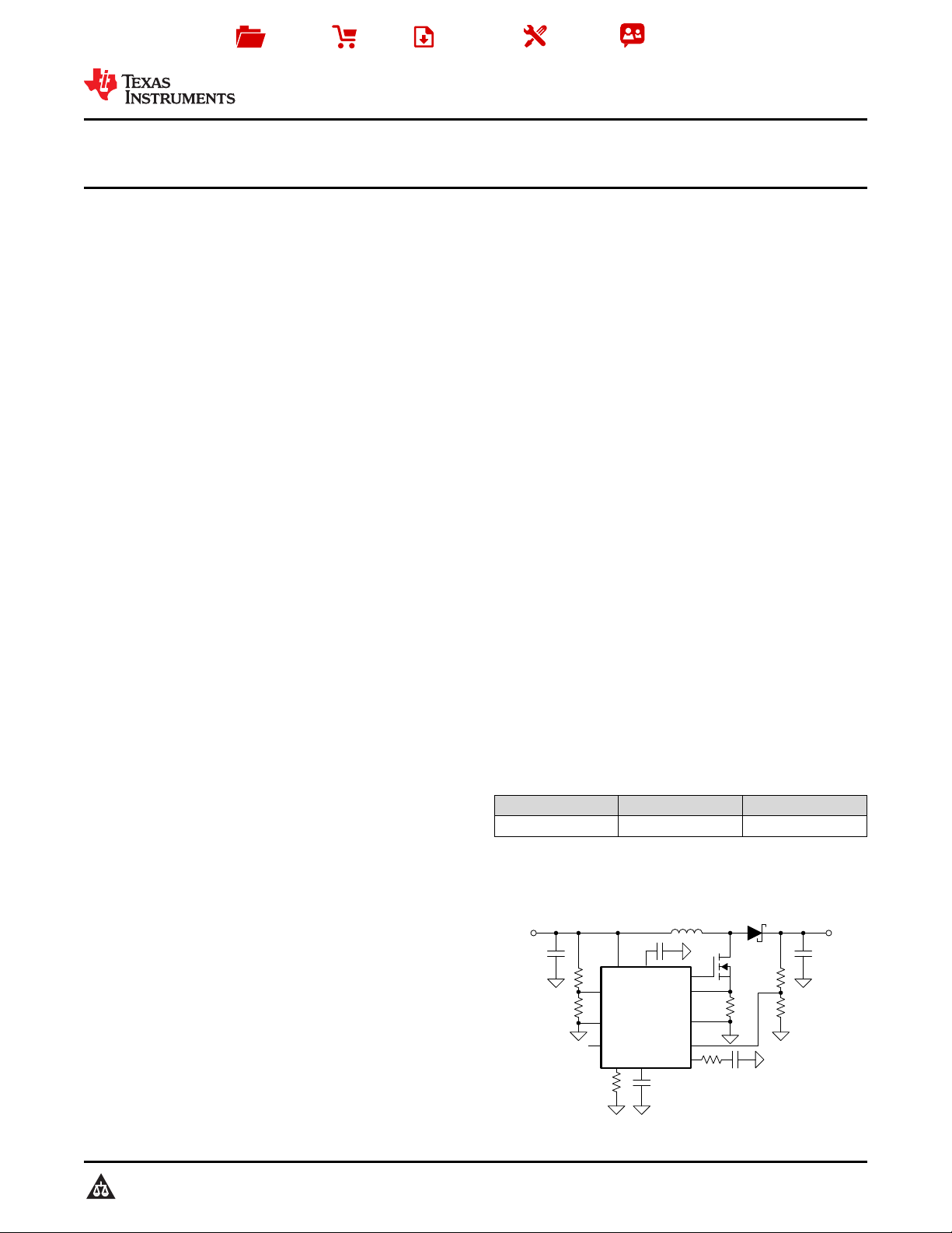
Typical Boost Application
– Dynamically programmable switching
frequency from 100 kHz to 2.2 MHz
• Integrated protection features
– Constant peak current limiting over input
voltage
– Optional hiccup mode overload protection (see
the Device Comparison Table)
– Programmable line UVLO
– OVP protection
1
– Thermal shutdown
An IMPORTANT NOTICE at the end of this data sheet addresses availability, warranty, changes, use in safety-critical applications,
intellectual property matters and other important disclaimers. PRODUCTION DATA.
Page 2

LM5156-Q1,LM51561-Q1
SNVSBI7A –JANUARY 2020–REVISED JUNE 2020
www.ti.com
Table of Contents
1 Features.................................................................. 1
2 Applications ........................................................... 1
3 Description ............................................................. 1
4 Revision History..................................................... 2
5 Description (continued)......................................... 3
6 Device Comparison Table..................................... 3
7 Pin Configuration and Functions......................... 4
8 Specifications......................................................... 5
8.1 Absolute Maximum Ratings ...................................... 5
8.2 ESD Ratings.............................................................. 5
8.3 Recommended Operating Conditions....................... 6
8.4 Thermal Information.................................................. 6
8.5 Electrical Characteristics........................................... 6
8.6 Typical Characteristics.............................................. 8
9 Detailed Description............................................ 11
9.1 Overview ................................................................. 11
9.2 Functional Block Diagram....................................... 11
9.3 Feature Description................................................. 12
9.4 Device Functional Modes........................................ 25
10 Application and Implementation........................ 26
10.1 Application Information.......................................... 26
10.2 Typical Application ................................................ 26
10.3 System Examples ................................................. 30
11 Power Supply Recommendations ..................... 36
12 Layout................................................................... 36
12.1 Layout Guidelines ................................................. 36
12.2 Layout Examples................................................... 37
13 Device and Documentation Support................. 39
13.1 Device Support...................................................... 39
13.2 Documentation Support ........................................ 39
13.3 Related Links ........................................................ 39
13.4 Receiving Notification of Documentation Updates 39
13.5 Support Resources ............................................... 40
13.6 Trademarks........................................................... 40
13.7 Electrostatic Discharge Caution............................ 40
13.8 Glossary................................................................ 40
14 Mechanical, Packaging, and Orderable
Information........................................................... 40
4 Revision History
NOTE: Page numbers for previous revisions may differ from page numbers in the current version.
Changes from Original (January 2020) to Revision A Page
• Changed device status from Advance Information to Production Data ................................................................................. 1
2
Submit Documentation Feedback Copyright © 2020, Texas Instruments Incorporated
Product Folder Links: LM5156-Q1 LM51561-Q1
Page 3
LM5156-Q1,LM51561-Q1
www.ti.com
SNVSBI7A –JANUARY 2020–REVISED JUNE 2020
5 Description (continued)
The internal VCC regulator also supports BIAS pin operation up to 60 V (65-V absolute maximum) for automotive
load dump. The switching frequency is dynamically programmable with an external resistor from 100 kHz to 2.2
MHz. Switching at 2.2 MHz minimizes AM band interference and allows for a small solution size and fast
transient response. To reduce the EMI of the power supply, the device provides a selectable dual random spread
spectrum which reduces the EMI over the wide frequency range.
The device features a 1.5-A standard MOSFET driver and a low 100-mV current limit threshold. The device also
supports the use of an external VCC supply to improve efficiency. Low operating current and pulse-skipping
operation improve efficiency at light loads.
The device has built-in protection features such as cycle-by-cycle current limit, overvoltage protection, line UVLO,
and thermal shutdown. Hiccup mode overload protection is available in the LM51561-Q1 device option.
Additional features include low shutdown IQ, programmable soft start, programmable slope compensation,
precision reference, power-good indicator, and external clock synchronization.
6 Device Comparison Table
DEVICE OPTION HICCUP MODE PROTECTION INTERNAL REFERENCE
LM5156-Q1 Disabled 1 V
LM51561-Q1 Enabled 1 V
Product Folder Links: LM5156-Q1 LM51561-Q1
Submit Documentation FeedbackCopyright © 2020, Texas Instruments Incorporated
3
Page 4
BIAS
GATE
VCC
GND
CS
COMP
PGOOD
UVLO/SYNC
SS
RT
FB
DITHOFF
1
2
3
4
5
6
7
8
9
10
11
12
EP
LM5156-Q1,LM51561-Q1
SNVSBI7A –JANUARY 2020–REVISED JUNE 2020
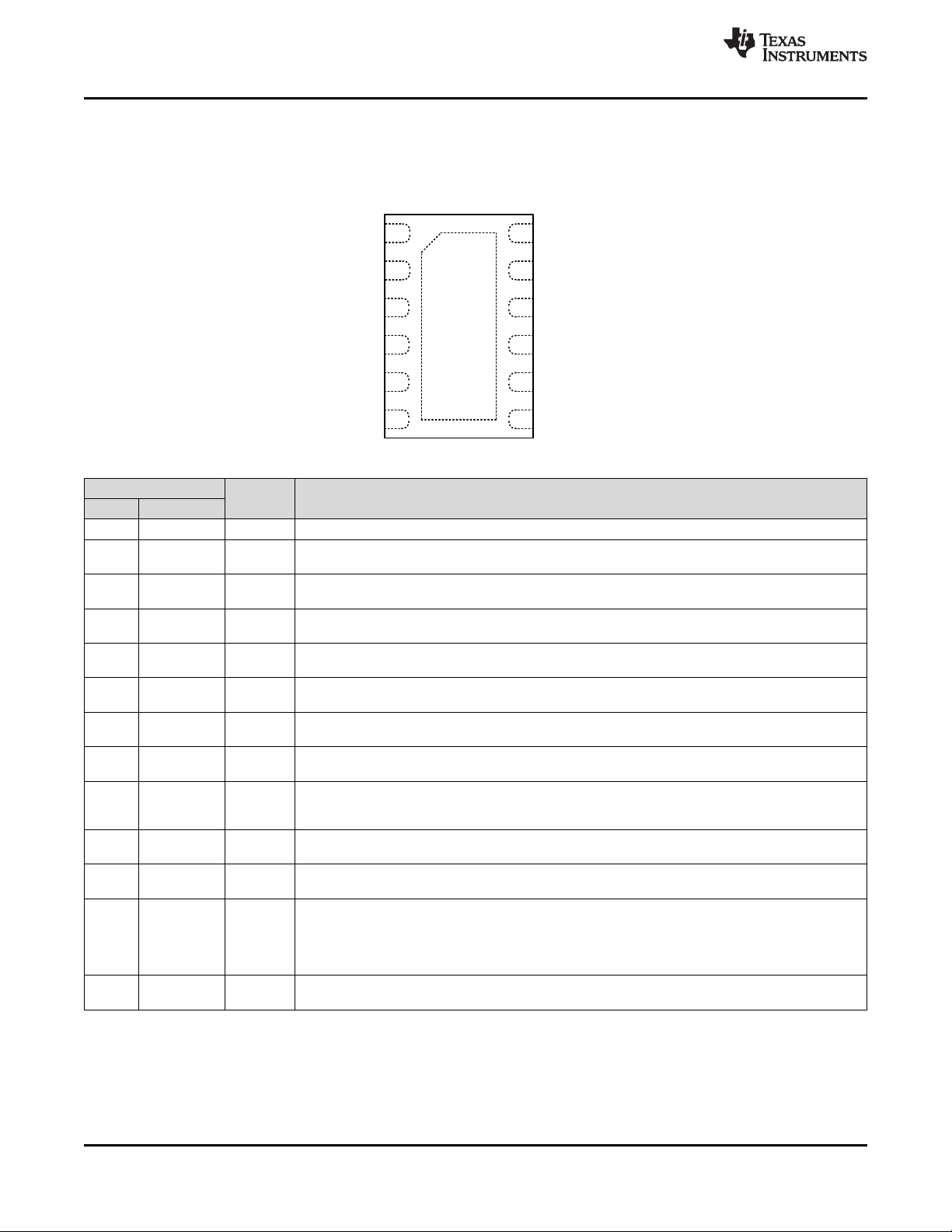
7 Pin Configuration and Functions
www.ti.com
12-Pin WSON With Wettable Flanks
DSS Package
Transparent Top View
Pin Functions
PIN
NO. NAME
1 BIAS P Supply voltage input to the VCC regulator. Connect a bypass capacitor from this pin to GND.
2 VCC P
3 GATE O
4 GND G
5 CS I
6 COMP O
7 DITHOFF I
8 FB I
9 SS I
10 RT I
11 PGOOD O
12
UVLO/SYNC/
EN
— EP —
(1) G = Ground, I = Input, O = Output, P = Power
TYPE
(1)
DESCRIPTION
Output of the internal VCC regulator and supply voltage input of the MOSFET driver. Connect a
ceramic bypass capacitor from this pin to GND.
N-channel MOSFET gate drive output. Connect directly to the gate of the N-channel MOSFET
through a short, low inductance path.
Ground pin. Connect directly to the ground connection of the sense resistor through a low inductance
wide and short path.
Current sense input pin. Connect to the positive side of the current sense resistor through a short
path.
Output of the internal transconductance error amplifier. Connect the loop compensation components
between this pin and GND.
Spread spectrum selection pin. Internal spread spectrum (Clock dithering) is disabled when the pin is
connected to the VCC pin. Connecting the pin to GND enables the internal spread spectrum.
Inverting input of the error amplifier. Connect a voltage divider from the output to this pin to set output
voltage in boost/SEPIC topologies. Connect the low-side feedback resistor to GND.
Soft-start time programming pin. An external capacitor and an internal current source set the ramp
rate of the internal error amplifier reference during soft start. Connect the ground connection of the
capacitor to GND.
Switching frequency setting pin. The switching frequency is programmed by a single resistor between
RT and GND.
Power-good indicator. An open-drain output which goes low if FB is below the under voltage
threshold. Connect a pullup resistor to the system voltage rail.
Undervoltage lockout programming pin. The converter start-up and shutdown levels can be
programmed by connecting this pin to the supply voltage through a resistor divider. The internal clock
I
can be synchronized to an external clock by applying a negative pulse signal into the
UVLO/SYNC/EN pin. This pin must not be left floating. Connect to BIAS pin if not used. Connect the
low-side UVLO resistor to GND.
Exposed pad of the package. The exposed pad must be connected to GND and the large ground
copper plane to decrease thermal resistance.
4
Submit Documentation Feedback Copyright © 2020, Texas Instruments Incorporated
Product Folder Links: LM5156-Q1 LM51561-Q1
Page 5
LM5156-Q1,LM51561-Q1
www.ti.com
SNVSBI7A –JANUARY 2020–REVISED JUNE 2020
8 Specifications
8.1 Absolute Maximum Ratings
Over the recommended operating junction temperature range
BIAS to GND –0.3 65
UVLO to GND –0.3 V
SS to GND
Input
RT to GND
FB to GND –0.3 4.0
CS to GND(DC) –0.3 0.3
CS to GND(50ns transient) –1
DITHOFF to GND -0.3 18
VCC to GND –0.3 18
Output
GATE to GND (50ns transient) –1
PGOOD to GND
COMP to GND
Junction temperature, T
Storage temperature, T
(1) Stresses beyond those listed under Absolute Maximum Ratings may cause permanent damage to the device. These are stress ratings
only, which do not imply functional operation of the device at these or any other conditions beyond those indicated under Recommended
Operating Conditions. Exposure to absolute-maximum-rated conditions for extended periods may affect device reliability.
(2) This pin is not specified to have an external voltage applied.
(3) 18 V or V
(4) The maximum current sink is limited to 1 mA when V
+ 0.3 V whichever is lower
BIAS
(5) This pin has an internal max voltage clamp which can handle up to 1.6 mA.
(6) High junction temperatures degrade operating lifetimes. Operating lifetime is de-rated for junction temperatures greater than 125°C.
(2)
(2)
(4)
(5)
(6)
J
stg
PGOOD>VBIAS
(1)
MIN MAX UNIT
+0.3
BIAS
–0.3 3.8
–0.3 3.8
(3)
–0.3 18
V
V
–0.3
–40 150
–55 150
°C
.
8.2 ESD Ratings
(1)
All pins ±500
Corner pins ±750
V
(ESD)
Electrostatic
discharge
Human-body model (HBM), per AEC Q100-002
HBM ESD Classification Level 2
Charged-device model (CDM), per AEC Q100-011
CDM ESD Classification Level C4B
(1) AEC Q100-002 indicates that HBM stressing shall be in accordance with the ANSI/ESDA/JEDEC JS-001 specification.
VALUE UNIT
±2000
V
Product Folder Links: LM5156-Q1 LM51561-Q1
Submit Documentation FeedbackCopyright © 2020, Texas Instruments Incorporated
5
Page 6
LM5156-Q1,LM51561-Q1
SNVSBI7A –JANUARY 2020–REVISED JUNE 2020
www.ti.com
8.3 Recommended Operating Conditions
Over the recommended operating junction temperature range
V
BIAS
V
VCC
V
DITHOFF
V
UVLO
V
FB
f
SW
f
SYNC
T
J
Bias input
VCC voltage
DITHOFF input 0 16 V
UVLO input 0 60 V
FB input 0 4.0 V
Typical switching frequency 100 2200 kHz
Synchronization pulse frequency 100 2200 kHz
Operating junction temperature
(1) Operating Ratings are conditions under the device is intended to be functional. For specifications and test conditions, see Electrical
Characteristics.
(2) BIAS pin operating range is from 2.97 V to 16 V when VCC is directly connected to BIAS. BIAS pin operating range is from 3.5 V to 60
V when VCC is supplied from the internal VCC regulator.
(3) This pin voltage should be less than V
(4) High junction temperatures degrade operating lifetimes. Operating lifetime is de-rated for junction temperatures greater than 125°C.
(2)
(3)
(4)
+ 0.3 V.
BIAS
(1)
MIN NOM MAX UNIT
2.97 60 V
2.97 16 V
–40 150 °C
8.4 Thermal Information
LM5156x-Q1
THERMAL METRIC
R
θJA
R
θJA
R
θJC(top)
R
θJB
ψ
JT
ψ
JT
ψ
JB
ψ
JB
R
θJC(bot)
Junction-to-ambient thermal resistance (LM5156EVM-BST) 33.2 °C/W
Junction-to-ambient thermal resistance 58.2 °C/W
Junction-to-case (top) thermal resistance 60.5 °C/W
Junction-to-board thermal resistance 27.2 °C/W
Junction-to-top characterization parameter (LM5156EVM-BST) 0.9 °C/W
Junction-to-top characterization parameter 1.8 °C/W
Junction-to-board characterization parameter (LM5156EVM-BST) 14.5 °C/W
Junction-to-board characterization parameter 27.2 °C/W
Junction-to-case (bottom) thermal resistance 4.7 °C/W
(1) For more information about traditional and new thermal metrics, see the Semiconductor and IC Package Thermal Metrics application
report.
(1)
UNITDSS(WSON)
12 PINS
8.5 Electrical Characteristics
Typical values correspond to TJ= 25°C. Minimum and maximum limits apply over TJ= -40°C to 125°C. Unless otherwise
stated, V
SUPPLY CURRENT
I
SHUTDOWN(BIAS)
I
OPERATING(BIAS)
VCC REGULATOR
V
VCC-REG
V
VCC-UVLO(RISING)
I
VCC-CL
ENABLE
V
EN(RISING)
V
EN(FALLING)
V
EN(HYS)
6
= 12V, RT= 9.09kΩ
BIAS
PARAMETER TEST CONDITIONS MIN TYP MAX UNIT
BIAS shutdown current V
BIAS operating current
VCC regulation V
VCC regulation V
= 12 V, V
BIAS
V
= 12 V, V
BIAS
V
, RT= 220 kΩ
REF
= 8 V, No load 6.5 6.85 7 V
BIAS
= 8 V, I
BIAS
= 0 V 2.6 5 uA
UVLO
= 2.0 V, VFB=
UVLO
= 35 mA 6.5 V
VCC
490 550 uA
VCC UVLO threshold VCC rising 2.75 2.85 2.95 V
VCC UVLO hysteresis VCC falling 0.063 V
VCC sourcing current limit V
BIAS
= 10 V, V
= 0 V 35 110 mA
VCC
Enable threshold EN rising 0.4 0.52 0.7 V
Enable threshold EN falling 0.33 0.49 0.63 V
Enable hysteresis EN falling 0.03 V
Submit Documentation Feedback Copyright © 2020, Texas Instruments Incorporated
Product Folder Links: LM5156-Q1 LM51561-Q1
Page 7
LM5156-Q1,LM51561-Q1
www.ti.com
SNVSBI7A –JANUARY 2020–REVISED JUNE 2020
Electrical Characteristics (continued)
Typical values correspond to TJ= 25°C. Minimum and maximum limits apply over TJ= -40°C to 125°C. Unless otherwise
stated, V
UVLO/SYNC
V
UVLO(RISING)
V
UVLO(FALLING)
V
UVLO(HYS)
I
UVLO
SPREAD SPECTRUM
V
DITHOFF(RISING)
V
DITHOFF(FALLING)
V
DITHOFF(HYS)
SS
I
SS
PULSE WIDTH MODULATION
fsw1 Switching frequency RT= 220 kΩ, V
fsw2 Switching frequency RT= 9.09 kΩ, V
t
ON(MIN)
D
MAX1
D
MAX2
CURRENT SENSE
I
SLOPE
V
CLTH
HICCUP MODE PROTECTION (LM51561)
ERROR AMPLIFIER
V
REF
Gm Transconductance 2 mA/V
OVP
V
OVTH
PGOOD
V
UVTH
MOSFET DRIVER
THERMAL SHUTDOWN
T
TSD
= 12V, RT= 9.09kΩ
BIAS
PARAMETER TEST CONDITIONS MIN TYP MAX UNIT
UVLO / SYNC threshold UVLO rising 1.425 1.5 1.575 V
UVLO / SYNC threshold UVLO falling 1.370 1.45 1.520 V
UVLO / SYNC threshold
hysteresis
UVLO hysteresis current V
Clock dithering threshold DITHOFF rising, V
Clock dithering threshold DITHOFF falling, V
Clock dithering threshold
hysteresis
Soft-start current 9 10 11 uA
SS pull-down switch R
Minimum on-time RT= 9.09 kΩ 50 ns
Maximum duty cycle limit RT= 9.09 kΩ, V
Maximum duty cycle limit RT= 220 kΩ, V
Peak slope compensation current RT= 220 kΩ 22.5 30 37.5 uA
Current Limit threshold (CS-
GND)
Hiccup enable cycles 64 Cycles
Hiccup timer reset cycles 8 Cycles
FB reference LM5156, LM51561 0.99 1 1.01 V
COMP sourcing current V
COMP clamp voltage COMP rising (V
COMP clamp voltage COMP falling 1 1.1 V
Over-voltage threshold FB rising (referece to V
Over-voltage threshold FB falling (referece to V
PGOOD pull-down switch R
Under-voltage threshold FB falling (referece to V
Under-voltage threshold FB rising (referece to V
High-state voltage drop 100 mA sinking 0.25 V
Low-state voltage drop 100 mA sourcing 0.15 V
Thermal shutdown threshold Temperature rising 175 °C
Thermal shutdown hysteresis 15 °C
DSON
UVLO falling 0.05 V
= 1.6 V 4 5 6 uA
UVLO
= 4 V 1.1 1.7 2.1 V
BIAS
= 4 V 0.6 1.2 1.8 V
BIAS
DITHOFF falling, V
= 4 V 0.5 V
BIAS
55 Ω
= 4 V 85 100 115 kHz
BIAS
= 4 V 1980 2200 2420 kHz
BIAS
= 4 V 80 85 90 %
BIAS
= 4 V 90 93 96 %
BIAS
93 100 107 mV
= 1.2V 180 uA
COMP
= 2.0 V) 2.5 2.8 V
UVLO
) 107 110 113 %
REF
) 105 %
REF
1 mA sinking 90 Ω
DSON
) 87 90 93 %
REF
) 95 %
REF
Product Folder Links: LM5156-Q1 LM51561-Q1
Submit Documentation FeedbackCopyright © 2020, Texas Instruments Incorporated
7
Page 8
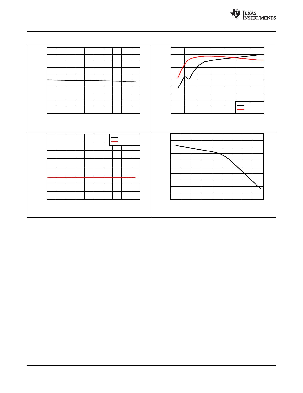
Duty Cycle (%)
Peak Inductor Current in Current Limit (A)
0 10 20 30 40 50 60 70 80 90 100
10
11
12
13
14
15
16
17
18
19
20
FSW=440kHz, RS=6m:, LM=1.2PH, V
LOAD
=10V
D005
RSL=0:
RSL=1k:
Temperature (qC)
Current Limit Threshold (mV)
-40 -20 0 20 40 60 80 100 120 140 160
95
96
97
98
99
100
101
102
103
104
105
D006
I
VCC
(mA)
V
VCC
(V)
0 20 40 60 80 100 120
0
1
2
3
4
5
6
7
D003
V
BIAS
(V)
Voltage (V)
0 2 4 6 8 10 12
0
2
4
6
8
10
12
D004
BIAS
VCC
RT Resistor (k:)
Frequency (kHz)
910 20 30 40 50 60 70 100 200 250
0
200
400
600
800
1000
1200
1400
1600
1800
2000
2200
2400
D001D001
Temperature (qC)
Frequency, RT=220k: (kHz)
Frequency, RT=9.09k: (kHz)
-40 -20 0 20 40 60 80 100 120 140 160
90 2000
92 2040
94 2080
96 2120
98 2160
100 2200
102 2240
104 2280
106 2320
108 2360
110 2400
RT=9.09kOhm
RT=220kOhm
D002
RT=220k:
RT=9.09k:
LM5156-Q1,LM51561-Q1
SNVSBI7A –JANUARY 2020–REVISED JUNE 2020
8.6 Typical Characteristics
Figure 1. Frequency vs RT Resistance Figure 2. Frequency vs Temperature
www.ti.com
Figure 3. V
VCC
vs I
Figure 5. Peak Current Limit vs Duty Cycle Figure 6. Current Limit Threshold vs Temperature
8
Submit Documentation Feedback Copyright © 2020, Texas Instruments Incorporated
VCC
Product Folder Links: LM5156-Q1 LM51561-Q1
Figure 4. V
VCC
vs V
BIAS
(No Load)
Page 9
Temperature (qC)
BIAS Shutdown Current (PA)
-40 -20 0 20 40 60 80 100 120 140 160
2.4
2.6
2.8
3
3.2
3.4
3.6
3.8
4
4.2
4.4
4.6
D011
BIAS=12V
BIAS=45V
Frequency (kHz)
Minimum On-Time (ns)
0 250 500 750 1000 1250 1500 1750 2000 2250 2500
40
60
80
100
120
140
160
180
200
D012
V
BIAS
(V)
BIAS Operating Current (PA)
5 10 15 20 25 30 35 40 45 50 55 60
470
480
490
500
510
520
530
D009
VFB=V
REF
, RT=221k:, V
VCC
=7V, COMP=1.75V
VBIAS (V)
BIAS Shutdown Current (PA)
0 5 10 15 20 25 30 35 40 45 50 55 60
0
0.5
1
1.5
2
2.5
3
3.5
4
4.5
D010
Temperature (qC)
FB Reference (V)
-40 -20 0 20 40 60 80 100 120 140 160
0.99
0.992
0.994
0.996
0.998
1
1.002
1.004
1.006
1.008
1.01
D007D007D007
Temperature (qC)
EN Threshold (V)
-40 -20 0 20 40 60 80 100 120 140 160
0.43
0.44
0.45
0.46
0.47
0.48
0.49
0.5
0.51
0.52
0.53
0.54
0.55
0.56
D008
EN Falling
EN Rising
www.ti.com
Typical Characteristics (continued)
Figure 7. FB Reference vs Temperature Figure 8. EN Threshold vs Temperature
LM5156-Q1,LM51561-Q1
SNVSBI7A –JANUARY 2020–REVISED JUNE 2020
Figure 9. I
OPERATING(BIAS)
Figure 11. I
Including RT Current vs V
SHUTDOWN
BIAS
Figure 10. I
vs Temperature Figure 12. t
Submit Documentation FeedbackCopyright © 2020, Texas Instruments Incorporated
Product Folder Links: LM5156-Q1 LM51561-Q1
SHUTDOWN(BIAS)
vs Frequency
ON(MIN)
vs V
BIAS
9
Page 10
Temperature (qC)
UVLO Threshold (V)
-40 -20 0 20 40 60 80 100 120 140 160
1.4
1.42
1.44
1.46
1.48
1.5
1.52
1.54
1.56
D015
UVLO rising
UVLO falling
Frequency (kHz)
Maximum Duty Cycle Limit (%)
0 250 500 750 1000 1250 1500 1750 2000 2250
85
86
87
88
89
90
91
92
93
94
95
D016
Temperature (qC)
Soft-Start Current (PA)
-40 -20 0 20 40 60 80 100 120 140 160
9
9.2
9.4
9.6
9.8
10
10.2
10.4
10.6
10.8
11
D013
V
VCC
(V)
Peak Driver Current (A)
2 4 6 8 10 12 14 16
0
0.2
0.4
0.6
0.8
1
1.2
1.4
1.6
1.8
2
D014
Isource (A)
Isink (A)
LM5156-Q1,LM51561-Q1
SNVSBI7A –JANUARY 2020–REVISED JUNE 2020
Typical Characteristics (continued)
Figure 13. ISSvs Temperature Figure 14. Peak Driver Current vs VCC
www.ti.com
Figure 15. UVLO Threshold vs Temperature Figure 16. Maximum Duty Cycle vs Frequency
10
Submit Documentation Feedback Copyright © 2020, Texas Instruments Incorporated
Product Folder Links: LM5156-Q1 LM51561-Q1
Page 11

BIAS
VCC
FB
PGOOD
V
LOAD
V
SUPPLY
+
±
+
±
V
OVTH
V
UVTH
VCC
Regulator
BIAS
VCC_EN
VCC
UVLO
VCC_OK
FB
C
IN
C
OUT
L
M
R
LOAD
Q1
D1
R
S
I
SLOPE
GATE
CS
V
CS1
V
CS2
S Q
Q
R
Clock
Generator
GND
Clock_Sync
+
±
+
±
V
CS1
V
CSTH
V
CS2
PWM Comparator
C/L Comparator
+
±
R
COMP
C
COMP
R
T
COMP
FB
SS
+
V
REF
I
SS
Optional
Hiccup Mode
I
UVLO
UVLO/
SYNC
+
±
+
±
V
EN
VCC_EN
SYNC
Detector
Clock_Sync
TSD
VCC_OK
RUN
V
SUPPLY
V
UVLO
C
SS
R
UVLOT
R
UVLOB
R
FBT
R
FBB
C
VCC
OVP
G
COMP
RT
OVP
TSD
DITHOFF
LM5156-Q1,LM51561-Q1
www.ti.com
SNVSBI7A –JANUARY 2020–REVISED JUNE 2020
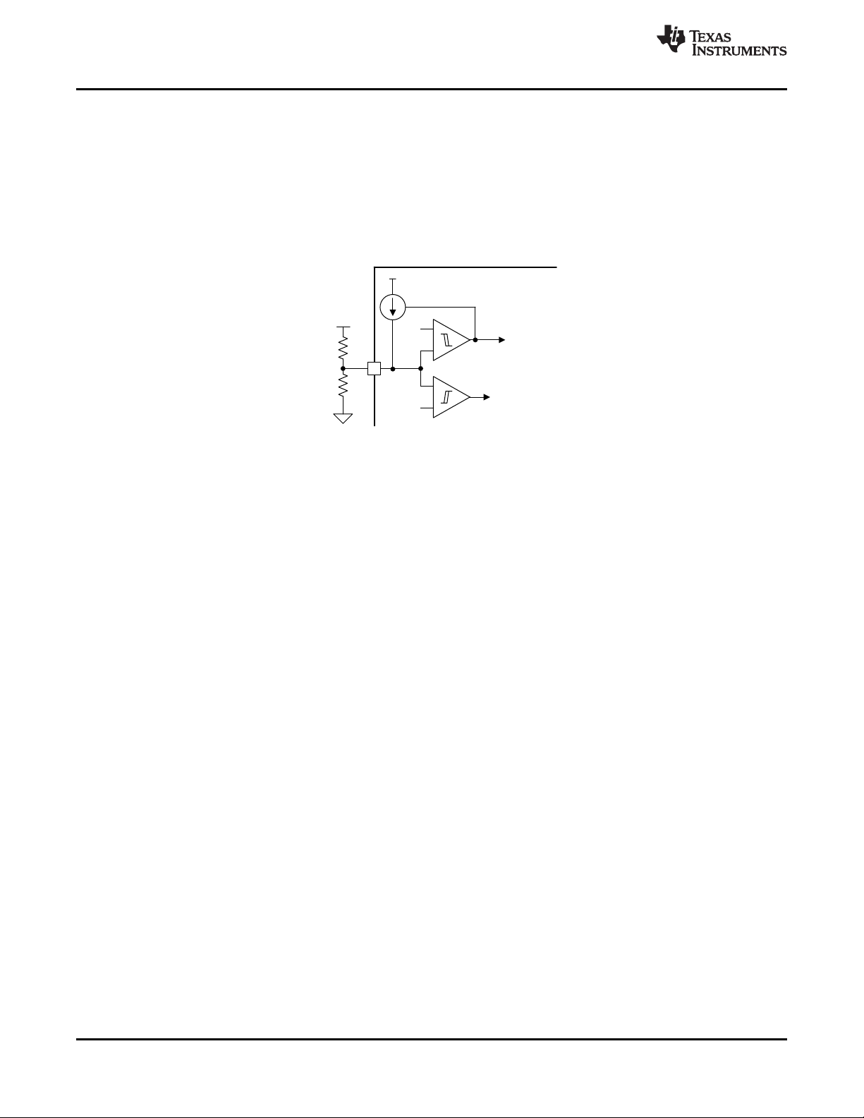
9 Detailed Description
9.1 Overview
The LM5156x-Q1 device is a wide input range, non-synchronous boost controller that uses peak-current-mode
control. The device can be used in boost, SEPIC, and flyback topologies.
The device can start up from a 1-cell battery with a minimum of 2.97 V if the BIAS pin is connected to the VCC
pin. It can operate with the input supply voltage as low as 1.5 V if the BIAS pin is greater than 3.5 V. The internal
VCC regulator also supports BIAS pin operation up to 60 V (65-V absolute maximum) for automotive load dump.
The switching frequency is dynamically programmable with an external resistor from 100 kHz to 2.2 MHz.
Switching at 2.2 MHz minimizes AM band interference and allows for a small solution size and fast transient
response. To reduce the EMI of the power supply, the device provides an optional dual random spread spectrum,
which reduces the EMI over the wide frequency span.
The device features a 1.5-A standard MOSFET driver and a low 100-mV current limit threshold. The device also
supports the use of an external VCC supply to improve efficiency. Low operating current and pulse skipping
operation improve efficiency at light loads.
The device has built-in protection features such as cycle-by-cycle current limit, overvoltage protection, line UVLO,
and thermal shutdown. Hiccup mode overload protection is available in the LM51561-Q1 device option.
Additional features include low shutdown IQ, programmable soft start, programmable slope compensation,
precision reference, power good indicator, and external clock synchronization.
9.2 Functional Block Diagram
Submit Documentation FeedbackCopyright © 2020, Texas Instruments Incorporated
11
Product Folder Links: LM5156-Q1 LM51561-Q1
Page 12
I
UVLO
UVLO/
SYNC
+
±
+
±
V
EN
VCC_EN
V
SUPPLY
V
UVLO
R
UVLOT
R
UVLOB
RUN
LM5156-Q1,LM51561-Q1
SNVSBI7A –JANUARY 2020–REVISED JUNE 2020
www.ti.com
9.3 Feature Description
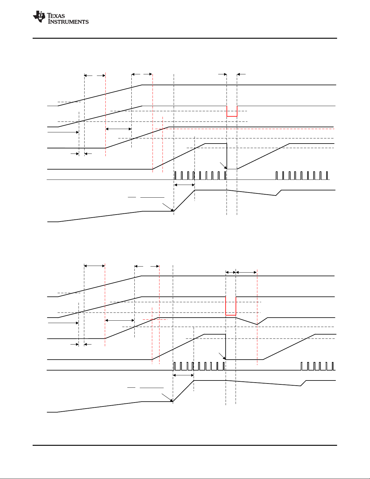
9.3.1 Line Undervoltage Lockout (UVLO/SYNC/EN pin)
The device has a dual-level UVLO circuit. During power-on, if the BIAS pin voltage is greater than 2.7 V, and the
UVLO pin voltage is in between the enable threshold (VEN) and the UVLO threshold (V
(see the Clock Synchronization (UVLO/SYNC/EN Pin) section for more details), the device starts up and an
internal configuration starts. The device typically requires a 65-µs internal start-up delay before entering standby
mode. In standby mode, the VCC regulator and RT regulator are operational, SS pin is grounded, and there is no
switching at the GATE output.
Figure 17. Line UVLO and Enable
) for more than 1.5 µs
UVLO
When the UVLO pin voltage is above the UVLO threshold, the device enters run mode. In the run mode, a softstart sequence starts if the VCC voltage is greater than 4.5 V, or 50 µs after the VCC voltage exceeds the 2.85-V
VCC UV threshold (V
VCC-UVLO
), whichever comes first. UVLO hysteresis is accomplished with an internal 50-mV
voltage hysteresis and an additional 5-μA current source that is switched on or off. When the UVLO pin voltage
exceeds the UVLO threshold, the current source is enabled to quickly raise the voltage at the UVLO pin. When
the UVLO pin voltage falls below the UVLO threshold, the current source is disabled, causing the voltage at the
UVLO pin to fall quickly. When the UVLO pin voltage is less than the enable threshold (VEN), the device enters
shutdown mode after a 35-µs (typical) delay with all functions disabled.
12
Submit Documentation Feedback Copyright © 2020, Texas Instruments Incorporated
Product Folder Links: LM5156-Q1 LM51561-Q1
Page 13
BIAS
= V
SUPPLY
UVLO
VCC
SS
GATE
2.7 V
0.52 V
2.85 V
50-µs
VCC UV delay
1.5 V
1 V
SS
1 V=V
LOAD(TARGET)
V
LOAD
Shutdown
Standby
t
SS
4.5 V
UVLO should be greater than
0.55 V more than 1.5µs to start-up
1.5 µs
65-µs (typical)
internal start-up delay
SS is grounded
with 2 cycles
delay
> 35 µs
V
LOAD
65-µs (typical)
internal start-up delay
UVLO
VCC
SS
V
LOAD
GATE
2.7 V
0.55 V
2.85 V
50-µs
VCC UV delay
1.5 V
1 V
SS
1 V
=
V
LOAD(TARGET)
V
LOAD
Shutdown
Standby
T
SS
4.5 V
UVLO should be greater than
0.55 V more than 1.5 µs to start-up
1.5 µs
> 3 cycles
SS is grounded
with 2 cycles
delay
65-µs (typical)
internal start-up delay
BIAS
= V
SUPPLY
www.ti.com
Feature Description (continued)
LM5156-Q1,LM51561-Q1
SNVSBI7A –JANUARY 2020–REVISED JUNE 2020
Figure 18. Boost Start-Up Waveforms
Case 1: Start-Up by 2.85-V VCC UVLO, UVLO Toggle After Start-Up
Figure 19. Boost Start-Up Waveforms
Case2: Start-Up When VCC > 4.5 V, EN Toggle After Start-Up
Submit Documentation FeedbackCopyright © 2020, Texas Instruments Incorporated
Product Folder Links: LM5156-Q1 LM51561-Q1
13
Page 14
V
SUPPLY
R
UVLOT
R
UVLOB
R
UVLOS
C
UVLO
I
UVLO
UVLO/SYNC
+
±
V
UVLO
RUN
UVLO(RISING) UVLOT
UVLOB
SUPPLY(ON) UVLO(RISING)
V R
R
V V
u
UVLO(FALLING)
SUPPLY(ON) SUPPLY(OFF)
UVLO(RISING)
UVLOT
UVLO
V
V V
V
R
I
u
LM5156-Q1,LM51561-Q1
SNVSBI7A –JANUARY 2020–REVISED JUNE 2020
www.ti.com
Feature Description (continued)
The external UVLO resistor divider must be designed so that the voltage at the UVLO pin is greater than 1.5 V
(typical) when the input voltage is in the desired operating range. The values of R
calculated as shown in Equation 1 and Equation 2.
where
• V
SUPPLY(ON)
• V
SUPPLY(OFF)
UVLO capacitor (C
is the desired start-up voltage of the converter.
is the desired turnoff voltage of the converter. (1)
) is required in case the input voltage drops below V
UVLO
SUPPLY(OFF)
up or during a severe load transient at the low input voltage. If the required UVLO capacitor is large, an
additional series UVLO resistor (R
) can be used to quickly raise the voltage at the UVLO pin when the 5-μA
UVLOS
hysteresis current turns on.
UVLOT
and R
UVLOB
can be
momentarily during start-
(2)
Figure 20. Line UVLO Using Three UVLO Resistors
Do not leave the UVLO pin floating. Connect to the BIAS pin if not used.
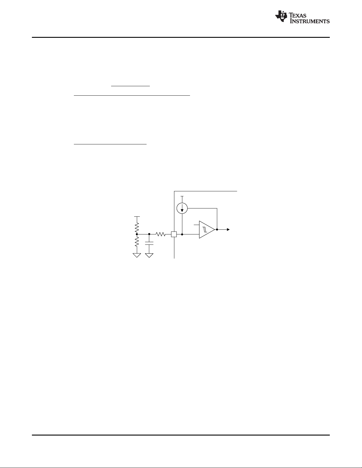
9.3.2 High Voltage VCC Regulator (BIAS, VCC Pin)
The device has an internal wide input VCC regulator which is sourced from the BIAS pin. The wide input VCC
regulator allows the BIAS pin to be connected directly to supply voltages from 3.5 V to 60 V.
The VCC regulator turns on when the device is in the standby or run mode. When the BIAS pin voltage is below
the VCC regulation target, the VCC output tracks the BIAS with a small dropout voltage. When the BIAS pin
voltage is greater than the VCC regulation target, the VCC regulator provides 6.85-V supply for the N-channel
MOSFET driver.
The VCC regulator sources current into the capacitor connected to the VCC pin with a minimum of 35-mA
capability. The recommended VCC capacitor value is from 1 µF to 4.7 µF.
The device supports a wide input range from 3.5 V to 60 V in normal configuration. By connecting the BIAS pin
directly to the VCC pin, the device supports inputs from 2.97 V to 16 V. This configuration is recommended when
the device starts up from a 1-cell battery.
14
Submit Documentation Feedback Copyright © 2020, Texas Instruments Incorporated
Product Folder Links: LM5156-Q1 LM51561-Q1
Page 15
BIAS
VCC
GATE
CS
GND
FB
COMP
SS
RT
PGOOD
DITHOFF
UVLO/SYNC
V
LOAD
V
SUPPLY
V
LOAD
UVLO > V
UVLO(RISING)
BIAS
VCC
GATE
CS
GND
FB
COMP
SS
RT
PGOOD
DITHOFF
UVLO/SYNC
V
LOAD
V
SUPPLY
(2.97V 16V)
LM5156-Q1,LM51561-Q1
www.ti.com
SNVSBI7A –JANUARY 2020–REVISED JUNE 2020
Feature Description (continued)
Figure 21. 2.97-V Start-Up (BIAS = VCC)
The minimum supply voltage after start-up can be further decreased by supplying the BIAS pin from the boost
converter output or from an external power supply as shown in Figure 22.
Figure 22. Decrease the Minimum Operating Voltage After Start-Up
In flyback topology, the internal power dissipation of the device can be decreased by supplying the VCC using an
additional transformer winding. In this configuration, the external VCC supply voltage must be greater than the
VCC regulation target (V
VCC-REG
), and the BIAS pin voltage must be greater the VCC voltage because the VCC
regulator includes a diode between VCC and BIAS.
Product Folder Links: LM5156-Q1 LM51561-Q1
Submit Documentation FeedbackCopyright © 2020, Texas Instruments Incorporated
15
Page 16

SS
SS
SS
C
tI
§ ·
u
¨ ¸
© ¹
SS SUPPLY
SS
SS LOAD
C V
t 1
I V
V
SUPPLY
BIAS
VCC
GATE
CS
GND
FB
COMP
SS
RT
PGOOD
DITHOFF
UVLO/SYNC
LM5156-Q1,LM51561-Q1
SNVSBI7A –JANUARY 2020–REVISED JUNE 2020
www.ti.com
Feature Description (continued)
Figure 23. External VCC Supply (BIAS ≥ VCC)
If the voltage of the external VCC bias supply is greater than the BIAS pin voltage, use an external blocking
diode from the input power supply to the BIAS pin to prevent the external bias supply from passing current to the
boost input supply through VCC.
9.3.3 Soft Start (SS pin)
The soft-start feature helps the converter gradually reach the steady state operating point, thus reducing start-up
stresses and surges. The device regulates the FB pin to the SS pin voltage or the internal reference, whichever
is lower.
At start-up, the internal 10-μA soft-start current source (ISS) turns on 50 µs after the VCC voltage exceeds the
2.85-VCC UV threshold, or if the VCC voltage is greater than 4.5 V, whichever comes first. The soft-start current
gradually increases the voltage on an external soft-start capacitor connected to the SS pin. This results in a
gradual rise of the output voltage. The SS pin is pulled down to ground by an internal switch when the VCC is
less than VCC UVLO threshold, the UVLO is less than the UVLO threshold, during hiccup mode off-time or
thermal shutdown.
In boost topology, soft-start time (tSS) varies with the input supply voltage. The soft-start time in boost topology is
calculated as shown in Equation 3.
(3)
In SEPIC topology, the soft-start time (tSS) is calculated as follows.
(4)
TI recommends choosing soft-start time long enough so that the converter can start up without going into an
overcurrent state. See the Hiccup Mode Overload Protection (LM51561-Q1 Only) section for more detailed
information.
Figure 24 shows an implementation of primary side soft start in flyback topology.
16
Submit Documentation Feedback Copyright © 2020, Texas Instruments Incorporated
Product Folder Links: LM5156-Q1 LM51561-Q1
Page 17

10
T
RT(TYPICAL)
2.21 10
R 955
f
u
V
LOAD
Secondary Side
Soft-start
FB
COMP
SS
www.ti.com
SNVSBI7A –JANUARY 2020–REVISED JUNE 2020
Feature Description (continued)
Figure 24. Primary-Side Soft Start in Flyback
Figure 25 shows an implementation of secondary side soft start in flyback topology.
LM5156-Q1,LM51561-Q1
Figure 25. Secondary-Side Soft Start in Flyback
9.3.4 Switching Frequency (RT Pin)
The switching frequency of the device can be set by a single RT resistor connected between the RT and the
GND pins. The resistor value to set the RT switching frequency (fRT) is calculated as shown in Equation 5.
(5)
The RT pin is regulated to 0.5 V by the internal RT regulator when the device is enabled.
9.3.5 Dual Random Spread Spectrum (DRSS)
The device provides a digital spread spectrum which reduces the EMI of the power supply over a wide frequency
range. This function is dynamically selectable during operation. The internal modulator dithers the internal clock
when the DITHOFF pin is less than 1.0 V or the pin is grounded, and it stops clock dithering when the DITHOFF
pin is greater than 2.0 V or the pin is connected to VCC. When an external synchronization clock is applied to the
SYNC pin, the internal spread spectrum is disabled. DRSS (a) combines a low-frequency triangular modulation
profile (b) with a high frequency cycle-by-cycle random modulation profile (c). The low frequency triangular
modulation improves performance in lower radio frequency bands (for example, the AM band), while the high
frequency random modulation improves performance in higher radio frequency bands (for example, the FM
band). In addition, the frequency of the triangular modulation is further modulated randomly to reduce the
likelihood of any audible tones. To minimize output voltage ripple caused by spread spectrum, duty cycle is
modified on a cycle-by-cycle basis to maintain a nearly constant duty cycle when dithering is enabled (see
Figure 26).
Product Folder Links: LM5156-Q1 LM51561-Q1
Submit Documentation FeedbackCopyright © 2020, Texas Instruments Incorporated
17
Page 18

UVLO/SYNC
V
SUPPLY
MCU
SHUTDOWN
DITHER ON
(DITHOFF=GND)
0.156 x f
SW
f
SW
(a) Low + High Frequency
Random Modulation
(b) Low Frequency
Random Modulation
(c) High Frequency
Random Modulation
DITHER OFF
(DITHOFF=VCC)
Frequency
LM5156-Q1,LM51561-Q1
SNVSBI7A –JANUARY 2020–REVISED JUNE 2020
Feature Description (continued)
Figure 26. Dual Random Spread Spectrum
www.ti.com
9.3.6 Clock Synchronization (UVLO/SYNC/EN Pin)
The switching frequency of the device can be synchronized to an external clock by pulling down the UVLO/SYNC
pin. The internal clock of the device is synchronized at the falling edge, but ignores the falling edge input during
the forced off-time which is determined by the maximum duty cycle limit. The external synchronization clock must
pull down the UVLO/SYNC pin voltage below 1.45 V (typical). The duty cycle of the pulldown pulse is not limited,
but the minimum pulldown pulse width must be greater than 150 ns, and the minimum pullup pulse width must be
greater than 250 ns. Figure 27 shows an implementation of the remote shutdown function. The UVLO pin can be
pulled down by a discrete MOSFET or an open-drain output of an MCU. In this configuration, the device stops
switching immediately after the UVLO pin is grounded, and the device shuts down 35 µs (typical) after the UVLO
pin is grounded.
Figure 27. UVLO and Shutdown
Figure 28 shows an implementation of shutdown and clock synchronization functions together. In this
configuration, the device stops switching immediately when the UVLO pin is grounded, and the device shuts
down if f
stays in high logic state for longer than 35 µs (typical) (UVLO is in low logic state for more than 35
SYNC
µs (typical)). The device runs at the f
if clock pulses are provided after the device is enabled.
SYNC
18
Submit Documentation Feedback Copyright © 2020, Texas Instruments Incorporated
Product Folder Links: LM5156-Q1 LM51561-Q1
Page 19

UVLO/SYNC
V
SUPPLY
MCU
F
SYNC
>0.7V
fSW [kHz]
Duty Cycle [%]
100 200 300 400 500 600 700 800 900 1000 1100
15
20
25
30
35
40
45
50
55
60
65
70
75
80
SUby
UVLO/SYNC
V
SUPPLY
MCU
F
SYNC
LM5156-Q1,LM51561-Q1
www.ti.com
SNVSBI7A –JANUARY 2020–REVISED JUNE 2020
Feature Description (continued)
Figure 28. UVLO, Shutdown, and Clock Synchronization
Figure 30 and Figure 31 show implementations of standby and clock synchronization functions together. In this
configuration, the device stops switching immediately if f
f
stays in high logic state for longer than two switching cycles. The device runs at f
SYNC
provided. Since the device can be enabled when the UVLO pin voltage is greater than the enable threshold for
more than 1.5 µs, the configurations in Figure 30 and Figure 31 are recommended if the external clock
synchronization pulses are provided from the start before the device is enabled. This 1.5-µs requirement can be
relaxed when the duty cycle of the synchronization pulse is greater than 50%. Figure 29 shows the required
minimum duty cycle to start up by synchronization pulses. When the switching frequency is greater than 1.1
MHz, the UVLO pin voltage should be greater than the enable threshold for more than 1.5 µs before applying the
external synchronization pulse.
stays in high logic state and enters standby mode if
SYNC
if clock pulses are
SYNC
Figure 29. Required Duty Cycle to Start Up by SYNC
Figure 30. UVLO, Standby, and Clock Synchronization (a)
Product Folder Links: LM5156-Q1 LM51561-Q1
Submit Documentation FeedbackCopyright © 2020, Texas Instruments Incorporated
19
Page 20

UVLO/SYNC
V
SUPPLY
LMV431
UVLO/SYNC
MCU
F
SYNC
10
MCU
F
SYNC
UVLO/SYNC
V
SUPPLY
LM5156-Q1,LM51561-Q1
SNVSBI7A –JANUARY 2020–REVISED JUNE 2020
www.ti.com
Feature Description (continued)
Figure 31. UVLO, Standby, and Clock Synchronization (b)
If the UVLO function is not required, the shutdown and clock synchronization functions can be implemented
together by using one push-pull output of the MCU. In this configuration, the device shuts down if f
low logic state for longer than 35 µs (typical). The device is enabled if f
than 1.5 µs. The device runs at the f
if clock pulses are provided after the device is enabled. Also, in this
SYNC
stays in high logic state for longer
SYNC
configuration, it is recommended to apply the external clock pulses after the BIAS is supplied. By limiting the
current flowing into the UVLO pin below 1 mA using a current limiting resistor, the external clock pulses can be
supplied before the BIAS is supplied (see Figure 32).
SYNC
stays in
Figure 32. Shutdown and Clock Synchronization
Figure 33 shows an implementation of inverted enable using external circuit.
Figure 33. Inverted UVLO
The external clock frequency (f
) must be within +25% and –30% of f
SYNC
RT(TYPICAL)
. Because the maximum duty
cycle limit and the peak current limit with slope resistor (RSL) are affected by the clock synchronization, take extra
care when using the clock synchronization function. See the Current Sense and Slope Compensation (CS Pin),
Current Limit and Minimum On-time (CS Pin), and Maximum Duty Cycle Limit and Minimum Input Supply Voltage
sections for more information.
20
Submit Documentation Feedback Copyright © 2020, Texas Instruments Incorporated
Product Folder Links: LM5156-Q1 LM51561-Q1
Page 21

RT
SLOPE
SYNC
f
V 40mV
f
u
RT
SLOPE
SYNC
f
I 30 A
f
P u
Sensed Inductor
Current (RS × ILM)
Fixed Slope
Compensation
Ramp
V
SLOPE
× D + 0.17V
Programmable Slope
Compensation Ramp
I
SLOPE
× RSL × D
V
Sensed Inductor
Current (RS × ILM)
Programmable Slope
Compensation Ramp
V
I
SLOPE
× RSL × D
R
S
I
SLOPE
CS
+
±
+
±
V
CS1
V
CSTH
V
CS2
PWM
Comparator
Current Limit
Comparator
COMP
G
COMP
R
F
(optional)
C
F
(optional)
R
SL
(optional)
=0.142
V
SLOPE
+ offset
R
COMP
C
COMP
C
HF
(optional)
LM5156-Q1,LM51561-Q1
www.ti.com
SNVSBI7A –JANUARY 2020–REVISED JUNE 2020
Feature Description (continued)
9.3.7 Current Sense and Slope Compensation (CS Pin)
The device has a low-side current sense and provides both fixed and optional programmable slope
compensation ramps, which help prevent subharmonic oscillation at high duty cycle. Both fixed and
programmable slope compensation ramps are added to the sensed inductor current input for the PWM operation.
But, only the programmable slope compensation ramp is added to the sensed inductor current input (see
Figure 34). For an accurate peak current limit operation over the input supply voltage, TI recommends using only
the fixed slope compensation (see Figure 5).
The device can generate the programmable slope compensation ramp using an external slope resistor (RSL) and
a sawtooth current source with a slope of 30 μA × fRT. This current flows out of the CS pin.
Figure 34. Current Sensing and Slope Compensation
Figure 35. Slope Compensation Ramp (a) at PWM
Comparator Input
Use Equation 6 to calculate the value of the peak slope current (I
of the peak slope voltage (V
where
• f
= fRTif clock synchronization is not used. (7)
SYNC
SLOPE
).
Figure 36. Slope Compensation Ramp (b) at Current Limit
Comparator Input
) and use Equation 7 to calculate the value
SLOPE
(6)
Product Folder Links: LM5156-Q1 LM51561-Q1
Submit Documentation FeedbackCopyright © 2020, Texas Instruments Incorporated
21
Page 22

F F
SW
1 D
3 R C
f
u u
15
ON(MIN)
6
T
800 10
t
1
4 10
8 R
u
|
u
u
SUPPLY
LOAD F
V
D 1
V V
RT
CLTH SL
SYNC
PEAK CL
S
f
V 30 A R D
f
I
R
P u u u
LOAD F SUPPLY
S SL SW
M
V V V
0.82 R 30uA R 40mV f
L
u u u u
LOAD F SUPPLY
S SW
M
V V V
0.5 R Margin 40mV f
L
u u u u
LM5156-Q1,LM51561-Q1
SNVSBI7A –JANUARY 2020–REVISED JUNE 2020
www.ti.com
Feature Description (continued)
According to peak current mode control theory, the slope of the compensation ramp must be greater than half of
the sensed inductor current falling slope to prevent subharmonic oscillation at high duty cycle. Therefore, the
minimum amount of slope compensation in boost topology should satisfy the following inequality:
where
• VFis a forward voltage drop of D1, the external diode. (8)
The recommended margin to cover non-ideal factors is 1.2. If required, RSLcan be added to further increase the
slope of the compensation ramp. Typically 82% of the sensed inductor current falling slope is known as an
optimal amount of the slope compensation. The RSLvalue to achieve 82% of the sensed inductor current falling
slope is calculated as shown in Equation 9.
(9)
If clock synchronization is not used, the fSWfrequency equals the fRTfrequency. If clock synchronization is used,
the fSWfrequency equals the f
9.3.8 Current Limit and Minimum On-time (CS Pin)
The device provides cycle-by-cycle peak current limit protection that turns off the MOSFET when the sum of the
inductor current and the programmable slope compensation ramp reaches the current limit threshold (V
Peak inductor current limit (I
PEAK-CL
frequency. The maximum value for the RSLresistance is 2 kΩ.
SYNC
) in steady state is calculated as shown in Equation 10.
CLTH
).
(10)
The practical duty cycle is greater than the estimated due to voltage drops across the MOSFET and sense
resistor. The estimated duty cycle is calculated as shown in Equation 11.
(11)
Boost converters have a natural pass-through path from the supply to the load through the high-side power diode
(D1). Because of this path and the minimum on-time limitation of the device, boost converters cannot provide
current limit protection when the output voltage is close to or less than the input supply voltage. The minimum
on-time is shown in Figure 12 and is calculated as Equation 12.
(12)
If required, a small external RC filter (RF, CF) at the CS pin can be added to overcome the large leading edge
spike of the current sense signal. Select an RFvalue in the range of 10 Ω to 200 Ω and a CFvalue in the range
of 100 pF to 2 nF. Because of the effect of this RC filter, the peak current limit is not valid when the on-time is
less than 2 × RF× CF. To fully discharge the CFduring the off-time, the RC time constant should satisfy the
following inequality.
(13)
22
Submit Documentation Feedback Copyright © 2020, Texas Instruments Incorporated
Product Folder Links: LM5156-Q1 LM51561-Q1
Page 23

64 cycles of
current limit
32768 hiccup
mode off cycles
60 cycles of
current limit
7 normal
switching
cycles
4 cycles of
current limit
Time
32768 hiccup
mode off cycles
Inductor Current
FBT
LOAD REF
FBB
R
V V 1
R
§ ·
u
¨ ¸
© ¹
LM5156-Q1,LM51561-Q1
www.ti.com
SNVSBI7A –JANUARY 2020–REVISED JUNE 2020
Feature Description (continued)
9.3.9 Feedback and Error Amplifier (FB, COMP Pin)
The feedback resistor divider is connected to an internal transconductance error amplifier which features high
output resistance (RO= 10 MΩ) and wide bandwidth (BW = 7 MHz). The internal transconductance error
amplifier sources current, which is proportional to the difference between the FB pin and the SS pin voltage or
the internal reference, whichever is lower. The internal transconductance error amplifier provides symmetrical
sourcing and sinking capability during normal operation and reduces its sinking capability when the FB is greater
than OVP threshold.
To set the output regulation target, select the feedback resistor values as shown in Equation 14.
(14)
The output of the error amplifier is connected to the COMP pin, allowing the use of a Type 2 loop compensation
network. R
phase characteristics to achieve a stable loop response. The absolute maximum voltage rating of the FB pin is
3.8 V. If necessary, especially during automotive load dump transient, the feedback resistor divider input can be
clamped with an external zener diode.
The COMP pin features internal clamps. The maximum COMP clamp limits the maximum COMP pin voltage
below its absolute maximum rating even in shutdown. The minimum COMP clamp limits the minimum COMP pin
voltage in order to start switching as soon as possible during no load to heavy load transition. The minimum
COMP clamp is disabled when FB is connected to ground in flyback topology.
COMP
, C
and optional CHFloop compensation components configure the error amplifier gain and
COMP
9.3.10 Power-Good Indicator (PGOOD pin)
The device has a power-good indicator (PGOOD) to simplify sequencing and supervision. The PGOOD switches
to a high impedance open-drain state when the FB pin voltage is greater than the feedback under voltage
threshold (V
), the VCC is greater than the VCC UVLO threshold and the UVLO/EN is greater than the EN
UVTH
threshold. A 25-μs deglitch filter prevents any false pulldown of the PGOOD due to transients. The recommended
minimum pullup resistor value is 10 kΩ.
Due to the internal diode path from the PGOOD pin to the BIAS pin, the PGOOD pin voltage cannot be greater
than V
BIAS
+ 0.3 V.
9.3.11 Hiccup Mode Overload Protection (LM51561-Q1 Only)
To further protect the converter during prolonged current limit conditions, the LM51561-Q1 device option provides
a hiccup mode overload protection. The internal hiccup mode fault timer of the device counts the PWM clock
cycles when the cycle-by-cycle current limiting occurs after soft start is finished. When the hiccup mode fault
timer detects 64 cycles of current limiting, an internal hiccup mode off timer forces the device to stop switching
and pulls down SS. Then, the device will restart after 32 768 cycles of hiccup mode off-time. The 64-cycle hiccup
mode fault timer is reset if eight consecutive switching cycles occur without exceeding the current limit threshold.
The soft-start time must be long enough not to trigger the hiccup mode protection after the soft start is finished.
To avoid an unexpected hiccup mode operation during a harsh load transient condition, it is recommended to
have more margin when programming the peak-current limit.
Figure 37. Hiccup Mode Overload Protection
Product Folder Links: LM5156-Q1 LM51561-Q1
Submit Documentation FeedbackCopyright © 2020, Texas Instruments Incorporated
23
Page 24

G@ VCC SW
Q f 35mAu
MAX2 SW
D 1 100ns f u
SYNC
MAX1
RT
f
D 1 0.1
f
u
SUPPLY(MIN) LOAD F MAX SUPPLY(MAX) DCR SUPPLY(MAX) DS(ON) S MAX
V V V 1 D I R I R R D| u u u u
LM5156-Q1,LM51561-Q1
SNVSBI7A –JANUARY 2020–REVISED JUNE 2020
www.ti.com
Feature Description (continued)
9.3.12 Maximum Duty Cycle Limit and Minimum Input Supply Voltage
When designing boost converters, the maximum duty cycle should be reviewed at the minimum supply voltage.
The minimum input supply voltage that can achieve the target output voltage is limited by the maximum duty
cycle limit, and it can be estimated as follows.
where
• I
SUPPLY(MAX)
• R
DCR
• R
DS(ON)
The minimum input supply voltage can be further decreased by supplying f
D
MAX1
or D
, whichever is lower.
MAX2
9.3.13 MOSFET Driver (GATE Pin)
The device provides an N-channel MOSFET driver that can source or sink a peak current of 1.5 A. The peak
sourcing current is larger when supplying an external VCC that is higher than 6.75 V VCC regulation target.
During start-up especially when the input voltage range is below the VCC regulation target, the VCC voltage
must be sufficient to completely enhance the MOSFET. If the MOSFET drive voltage is lower than the MOSFET
gate plateau voltage during start-up, the boost converter may not start up properly and it can stick at the
maximum duty cycle in a high power dissipation state. This condition can be avoided by selecting a lower
threshold N-channel MOSFET switch and setting the V
regulator has a limited sourcing capability, the MOSFET gate charge should satisfy the following inequality.
is the maximum input current.
is the DC resistance of the inductor.
is the on-resistance of the MOSFET. (15)
, which is less than fRT. D
SYNC
SUPPLY(ON)
greater than 6 to 7 V. Because the internal VCC
(16)
(17)
MAX
is
(18)
An internal 1-MΩ resistor is connected between GATE and GND to prevent a false turnon during shutdown. In
boost topology, switch node dV/dT must be limited during the 65-µs internal start-up delay to avoid a false
turnon, which is caused by the coupling through CDGparasitic capacitance of the MOSFET.
9.3.14 Overvoltage Protection (OVP)
The device has OVP for the output voltage. OVP is sensed at the FB pin. If the voltage at the FB pin rises above
the overvoltage threshold (V
), OVP is triggered and switching stops. During OVP, the internal error amplifier
OVTH
is operational, but the maximum source and sink capability is decreased to 40 µA.
9.3.15 Thermal Shutdown (TSD)
An internal thermal shutdown turns off the VCC regulator, disables switching, and pulls down the SS when the
junction temperature exceeds the thermal shutdown threshold (T
). After the temperature is decreased by
TSD
15°C, the VCC regulator is enabled again and the device performs a soft start.
24
Submit Documentation Feedback Copyright © 2020, Texas Instruments Incorporated
Product Folder Links: LM5156-Q1 LM51561-Q1
Page 25

LM5156-Q1,LM51561-Q1
www.ti.com
SNVSBI7A –JANUARY 2020–REVISED JUNE 2020
9.4 Device Functional Modes
9.4.1 Shutdown Mode
If the UVLO pin voltage is below the enable threshold for longer than 35 µs (typical), the device goes to the
shutdown mode with all functions disabled. In shutdown mode, the device decreases the BIAS pin current
consumption to below 2.6 μA (typical)
9.4.2 Standby Mode
If the UVLO pin voltage is greater than the enable threshold and below the UVLO threshold for longer than 1.5
µs, the device is in standby mode with the VCC regulator operational, RT regulator operational, SS pin grounded,
and no switching at the GATE output. The PGOOD is activated when the VCC voltage is greater than the VCC
UV threshold.
9.4.3 Run Mode
If the UVLO pin voltage is above the UVLO threshold and the VCC voltage is sufficient, the device enters RUN
mode. In this mode, soft start starts 50 µs after the VCC voltage exceeds the 2.85 VCC UV threshold, or if the
VCC voltage is greater than 4.5 V, whichever comes first.
Product Folder Links: LM5156-Q1 LM51561-Q1
Submit Documentation FeedbackCopyright © 2020, Texas Instruments Incorporated
25
Page 26

BIAS
VCC
GATE
CS
GND
FB
COMP
SS
RT
PGOOD
DITHOFF
UVLO/SYNC
V
LOAD
V
SUPPLY
MCU_VCC
L
M
C
IN
C
OUT1
R
LOAD
Q1
D1
R
S
R
COMP
C
COMP
R
T
C
SS
R
UVLOT
R
UVLOS
R
FBT
R
FBB
C
VCC
C
OUT2
+
±
C
HF
R
UVLOB
C
F
R
F
R
SL
R
G
D
G
R
PG
R
BIAS
C
BIAS
C
UVLO
R
SNB
C
SNB
LM5156-Q1,LM51561-Q1
SNVSBI7A –JANUARY 2020–REVISED JUNE 2020
www.ti.com
10 Application and Implementation
NOTE
Information in the following applications sections is not part of the TI component
specification, and TI does not warrant its accuracy or completeness. TI’s customers are
responsible for determining suitability of components for their purposes. Customers should
validate and test their design implementation to confirm system functionality.
10.1 Application Information
How to Design a Boost Converter Using LM5156x explains how to design boost, SEPIC, and Flyback converters
using the device. This comprehensive application note includes component selections and loop response
optimization.
10.2 Typical Application
Figure 38 shows all optional components to design a boost converter.
Figure 38. Typical Boost Converter Circuit With Optional Components
10.2.1 Design Requirements
Table 1 shows the intended input, output, and performance parameters for this application example.
Table 1. Design Example Parameters
DESIGN PARAMETER VALUE
Minimum input supply voltage (V
Target output voltage (V
Maximum load current (I
Typical switching frequency (fSW) 440 kHz
10.2.2 Detailed Design Procedure
SUPPLY(MIN)
LOAD
LOAD
Use the LM5155x / LM5156x Boost Quick Start Calculator to expedite the process of designing of a regulator for
a given application based on the LM5156x-Q1 device.
The LM5156x-Q1 device is also WEBENCH® Designer enabled. The WEBENCH software uses an iterative
design procedure and accesses comprehensive data bases of components when generating a design.
26
Submit Documentation Feedback Copyright © 2020, Texas Instruments Incorporated
Product Folder Links: LM5156-Q1 LM51561-Q1
) 6 V
) 24 V
) 2 A (≈ 48 Watt)
Page 27

LM5156-Q1,LM51561-Q1
www.ti.com
SNVSBI7A –JANUARY 2020–REVISED JUNE 2020
10.2.2.1 Custom Design With WEBENCH® Tools
Click here to create a custom design using the LM5156x-Q1 device with the WEBENCH® Power Designer.
1. Start by entering the input voltage (VIN), output voltage (V
), and output current (I
OUT
) requirements.
OUT
2. Optimize the design for key parameters such as efficiency, footprint, and cost using the optimizer dial.
3. Compare the generated design with other possible solutions from Texas Instruments.
The WEBENCH Power Designer provides a customized schematic along with a list of materials with real-time
pricing and component availability.
In most cases, these actions are available:
• Run electrical simulations to see important waveforms and circuit performance
• Run thermal simulations to understand board thermal performance
• Export customized schematic and layout into popular CAD formats
• Print PDF reports for the design, and share the design with colleagues
Get more information about WEBENCH tools at www.ti.com/WEBENCH.
10.2.2.2 Recommended Components
Table 2 shows a recommended list of materials for this typical application.
(1)
Coilcraft XAL1010-682MEB
Chemi-Con HHXB500ARA101MJA0G
Panasonic EEHZC1H101P
REFERENCE
DESIGNATOR
R
T
R
FBT
R
FBB
L
M
R
S
R
SL
C
OUT1
C
(Bulk) 2
OUT2
C
IN1
C
(Bulk) 1
IN2
Table 2. List of Materials
QTY. SPECIFICATION MANUFACTURER PART NUMBER
1 RES, 49.9 k, 1%, 0.1 W, AEC-Q200 Grade 0, 0603 Vishay-Dale CRCW060349K9FKEA
1 RES, 47.0 k, 1%, 0.1 W, AEC-Q200 Grade 0, 0603 Vishay-Dale CRCW060347K0FKEA
1 RES, 2.0 k, 5%, 0.1 W, AEC-Q200 Grade 0, 0603 Vishay-Dale CRCW06032K00JNEA
Inductor, Shielded, Composite, 6.8 µH, 18.5 A, 0.01 Ω,
1
1 RES, 0.008, 1%, 3 W, AEC-Q200 Grade 0, 2512 WIDE Susumu KRL6432E-M-R008-F-T1
1 RES, 0, 5%, 0.1 W, 0603 Yageo America RC0603JR-070RL
3 CAP, CERM, 4.7 µF, 50 V, ±10%, X7R, 1210 TDK C3225X7R1H475K250AB
CAP, Aluminum Polymer, 100 µF, 50 V, ±20%, 0.025 Ω,
AEC-Q200 Grade 2, D10xL10mm SMD
6 CAP, CERM, 10 µF, 50 V, ±10%, X7R, 1210 MuRata GRM32ER71H106KA12L
CAP, Polymer Hybrid, 100 µF, 50 V, ±20%, 28 Ω, 10x10
SMD
SMD
Q1 1 MOSFET, N-CH, 40 V, 50 A, AEC-Q101, SON-8 Infineon IPC50N04S5L5R5ATMA1
D1 1 Schottky, 60 V, 10 A, AEC-Q101, CFP15 Nexperia PMEG060V100EPDZ
R
COMP
C
COMP
C
R
UVLOT
R
UVLOB
R
UVLOS
C
R
D
R
C
R
SNB
HF
SS
G
G
F
F
1 RES, 11.3 k, 1%, 0.1 W, AEC-Q200 Grade 0, 0603 Vishay-Dale CRCW060311K3FKEA
CAP, CERM, 0.022 µF, 100 V, ±10%, X7R, AEC-Q200
1
CAP, CERM, 220 pF, 20 V, ±5%, C0G/NP0, AEC-Q200
1
Grade 1, 0603
Grade 1, 0603
TDK CGA3E2X7R2A223K080AA
TDK CGA3E2C0G1H221J080AA
1 RES, 21.0 k, 1%, 0.1 W, AEC-Q200 Grade 0, 0603 Vishay-Dale CRCW060321K0FKEA
1 RES, 7.32 k, 1%, 0.1 W, AEC-Q200 Grade 0, 0603 Vishay-Dale CRCW06037K32FKEA
0 N/A N/A N/A
1
CAP, CERM, 0.22 µF, 50 V, ±10%, X7R, AEC-Q200
Grade 1, 0603
TDK CGA3E3X7R1H224K080AB
0 N/A N/A N/A
1 RES, 0, 5%, 0.1 W, 0603 Yageo America RC0603JR-070RL
1 CAP, CERM, 100 pF, 50 V, ±1%, C0G/NP0, 0603 Kemet C0603C101F5GACTU
1 RES, 100, 1%, 0.1 W, 0603 Yageo America RC0603FR-07100RL
0 N/A N/A N/A
(1) See Third-party Products Disclaimer
Product Folder Links: LM5156-Q1 LM51561-Q1
Submit Documentation FeedbackCopyright © 2020, Texas Instruments Incorporated
27
Page 28

TOTAL IC Q D L RS
P P P P P P
LM5156-Q1,LM51561-Q1
SNVSBI7A –JANUARY 2020–REVISED JUNE 2020
www.ti.com
Table 2. List of Materials()(continued)
REFERENCE
DESIGNATOR
C
SNB
R
BIAS
C
BIAS
C
VCC
R
PG
QTY. SPECIFICATION MANUFACTURER PART NUMBER
0 N/A N/A N/A
1 RES, 0, 5%, 0.1 W, AEC-Q200 Grade 0, 0603 Panasonic ERJ-3GEY0R00V
1 CAP, CERM, 0.01 µF, 50 V, ±10%, X7R, 0603
CAP, CERM, 1 µF, 16 V, ±20%, X7R, AEC-Q200 Grade
1
1 RES, 24.9 k, 1%, 0.1 W, 0603 Yageo America RC0603FR-0724K9L
1, 0603
Samsung Electro-
Mechanics
MuRata GCM188R71C105MA64D
CL10B103KB8NCNC
10.2.2.3 Inductor Selection (LM)
When selecting the inductor, consider three key parameters: inductor current ripple ratio (RR), falling slope of the
inductor current, and RHP zero frequency (f
RHP
).
Inductor current ripple ratio is selected to have a balance between core loss and copper loss. The falling slope of
the inductor current must be low enough to prevent subharmonic oscillation at high duty cycle (additional R
resistor is required if not). Higher f
(= lower inductance) allows a higher crossover frequency and is always
RHP
SL
preferred when using a small value output capacitor.
The inductance value can be selected to set the inductor current ripple between 30% and 70% of the average
inductor current as a good compromise between RR, F
, and inductor falling slope.
RHP
10.2.2.4 Output Capacitor (C
There are a few ways to select the proper value of output capacitor (C
OUT
)
). The output capacitor value can be
OUT
selected based on output voltage ripple, output overshoot, or undershoot due to load transient.
The ripple current rating of the output capacitors must be enough to handle the output ripple current. By using
multiple output capacitors, the ripple current can be split. In practice, ceramic capacitors are placed closer to the
diode and the MOSFET than the bulk aluminum capacitors to absorb the majority of the ripple current.
10.2.2.5 Input Capacitor
The input capacitors decrease the input voltage ripple. The required input capacitor value is a function of the
impedance of the source power supply. More input capacitors are required if the impedance of the source power
supply is not low enough.
10.2.2.6 MOSFET Selection
The MOSFET gate driver of the device is sourced from VCC. The maximum gate charge is limited by the 35-mA
VCC sourcing current limit.
A leadless package is preferred for high switching-frequency designs. The MOSFET gate capacitance should be
small enough so that the gate voltage is fully discharged during the off-time.
10.2.2.7 Diode Selection
A Schottky is the preferred type for D1 diode due to its low forward voltage drop and small reverse recovery
charge. Low reverse leakage current is an important parameter when selecting the Schottky diode. The diode
must be rated to handle the maximum output voltage plus any switching node ringing. Also, it must be able to
handle the average output current.
10.2.2.8 Efficiency Estimation
The total loss of the boost converter (P
MOSFET power losses (PQ), diode power losses (PD), inductor power losses (PL), and the loss in the sense
resistor (PRS).
PICcan be separated into gate driving loss (PG) and the losses caused by quiescent current (PIQ).
28
Submit Documentation Feedback Copyright © 2020, Texas Instruments Incorporated
) can be expressed as the sum of the losses in the device (PIC),
TOTAL
Product Folder Links: LM5156-Q1 LM51561-Q1
(19)
Page 29

2
RS SUPPLY S
P D I R u u
SUPPLY
SW
M
1
V D
f
I
L
u u
'
AC SW
P K I f
E D
u ' u
2
DCR SUPPLY DCR
P I R u
L DCR AC
P P P
RR LOAD RR SW
P V Q f u u
VF F SUPPLY
P (1 D) V I u u
D VF RR
P P P
2
Q(COND) SUPPLY DS(ON)
P D I R u u
Q(SW) LOAD F SUPPLY R F SW
P 0.5 (V V ) I (t t ) f u u u u
Q Q(SW) Q(COND)
P P P
IQ BIAS BIAS
P V I u
G G(@ VCC) BIAS SW
P Q V f u u
IC G IQ
P P P
www.ti.com
SNVSBI7A –JANUARY 2020–REVISED JUNE 2020
Each power loss is approximately calculated as follows:
I
and I
VIN
PQcan be separated into switching loss (P
values in each mode can be found in the supply current section of the Electrical Characteristics.
VOUT
) and conduction loss (P
Q(SW)
Q(COND)
).
Each power loss is approximately calculated as follows:
tRand tFare the rise and fall times of the low-side N-channel MOSFET device. I
SUPPLY
of the boost converter.
R
is the on-resistance of the MOSFET and is specified in the MOSFET data sheet. Consider the R
DS(ON)
increase due to self-heating.
PDcan be separated into diode conduction loss (PVF) and reverse recovery loss (PRR).
LM5156-Q1,LM51561-Q1
(20)
(21)
(22)
(23)
(24)
is the input supply current
(25)
DS(ON)
(26)
Each power loss is approximately calculated as follows:
(27)
(28)
QRRis the reverse recovery charge of the diode and is specified in the diode data sheet. Reverse recovery
characteristics of the diode strongly affect efficiency, especially when the output voltage is high.
PLis the sum of DCR loss (P
) and AC core loss (PAC). DCR is the DC resistance of inductor which is
DCR
mentioned in the inductor data sheet.
(29)
Each power loss is approximately calculated as follows:
(30)
(31)
(32)
∆I is the peak-to-peak inductor current ripple. K, α, and β are core dependent factors which can be provided by
the inductor manufacturer.
PRSis calculated as follows:
Efficiency of the power converter can be estimated as follows:
Product Folder Links: LM5156-Q1 LM51561-Q1
(33)
Submit Documentation FeedbackCopyright © 2020, Texas Instruments Incorporated
29
Page 30

BIAS
VCC
GATE
CS
GND
FB
COMP
SS
RT
PGOOD
DITHOFF
UVLO/SYNC
V
LOAD
V
SUPPLY
I
LOAD
[A]
Efficiency [%]
0 0.2 0.4 0.6 0.8 1 1.2 1.4 1.6 1.8 2
76
78
80
82
84
86
88
90
92
94
96
98
BSTEBSTEBSTE
V
SUPPLY
=18V
V
SUPPLY
=12V
V
SUPPLY
=9V
V
SUPPLY
=6V
LOAD LOAD
TOTAL LOAD LOAD
V I
Efficiency
P V I
u
u
LM5156-Q1,LM51561-Q1
SNVSBI7A –JANUARY 2020–REVISED JUNE 2020
10.2.3 Application Curve
10.3 System Examples
www.ti.com
(34)
Figure 39. Efficiency
30
Submit Documentation Feedback Copyright © 2020, Texas Instruments Incorporated
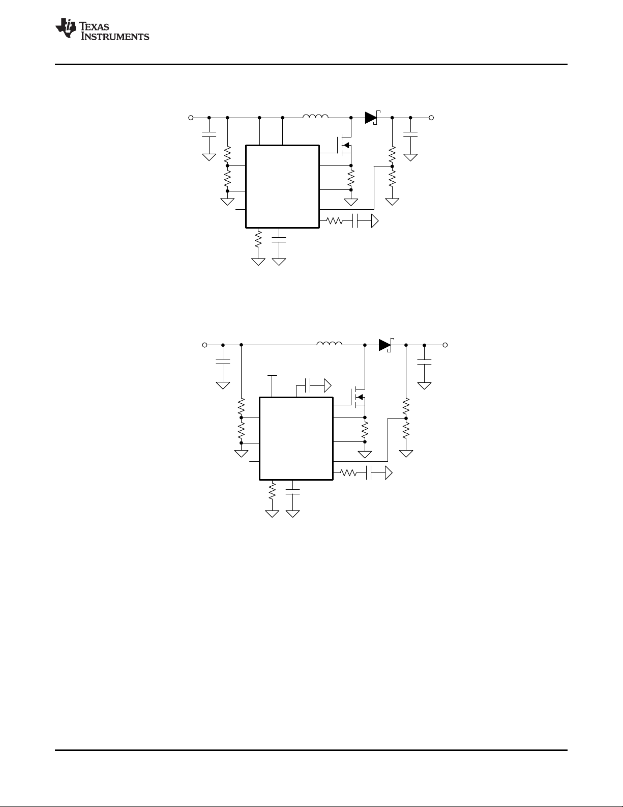
Figure 40. Typical Boost Application
Product Folder Links: LM5156-Q1 LM51561-Q1
Page 31

BIAS
VCC
GATE
CS
GND
FB
COMP
SS
RT
PGOOD
DITHOFF
UVLO/SYNC
V
LOAD
V
SUPPLY
Optional
-
+
= 2.97V - 16V
BIAS
VCC
GATE
CS
GND
FB
COMP
SS
RT
PGOOD
DITHOFF
UVLO/SYNC
V
LOAD
V
SUPPLY
From MCU
1-cell or
2-cell
Battery
= 12V / 24V
-
+
= 3.5V - 60V
BIAS
VCC
GATE
CS
GND
FB
COMP
SS
RT
PGOOD
DITHOFF
UVLO/SYNC
V
LOAD
V
SUPPLY
From MCU
To MCU
Car
Battery
Optional
www.ti.com
System Examples (continued)
LM5156-Q1,LM51561-Q1
SNVSBI7A –JANUARY 2020–REVISED JUNE 2020
Figure 41. Typical Start-Stop Application
Figure 42. Emergency-call / Boost On-Demand / Portable Speaker
Figure 43. Typical SEPIC Application
Product Folder Links: LM5156-Q1 LM51561-Q1
Submit Documentation FeedbackCopyright © 2020, Texas Instruments Incorporated
31
Page 32

BIAS
VCC
GATE
CS
GND
FB
COMP
SS
RT
PGOOD
DITHOFF
UVLO/SYNC
V
LOAD
V
SUPPLY
> 150V-200V
Voltage
Tripler
Inductance should be big enough
to operate in CCM
BIAS
VCC
GATE
CS
GND
FB
COMP
SS
RT
PGOOD
DITHOFF
UVLO/SYNC
V
LOAD
V
SUPPLY
From MCU
= 30V-150V
Inductance should be small enough
to operate in DCM at full load
LM5156-Q1,LM51561-Q1
SNVSBI7A –JANUARY 2020–REVISED JUNE 2020
System Examples (continued)
www.ti.com
Figure 44. LIDAR Bias Supply 1
32
Submit Documentation Feedback Copyright © 2020, Texas Instruments Incorporated
Figure 45. LIDAR Bias Supply 2
Product Folder Links: LM5156-Q1 LM51561-Q1
Page 33

BIAS
VCC
GATE
CS
GND
FB
COMPSS
RT
PGOOD
DITHOFF
UVLO/SYNC
V
LOAD
V
SUPPLY
Optional Primary-Side
Soft-Start
= 5V/12V
BIAS
VCC
GATE
CS
GND
FB
COMP
SS
RT
PGOOD
DITHOFF
UVLO/SYNC
V
LOAD
V
SUPPLY
System Power
To MCU
(Fault Indicator)
www.ti.com
System Examples (continued)
LM5156-Q1,LM51561-Q1
SNVSBI7A –JANUARY 2020–REVISED JUNE 2020
Figure 46. Low-Cost LED Driver
Figure 47. Secondary-Side Regulated Isolated Flyback
Product Folder Links: LM5156-Q1 LM51561-Q1
Submit Documentation FeedbackCopyright © 2020, Texas Instruments Incorporated
33
Page 34

BIAS
VCC
GATE
CS
GND
FB
COMP
SS
RT
PGOOD
DITHOFF
UVLO/SYNC
V
SUPPLY
System Power
To MCU
V
LOAD
BIAS
VCC
GATE
CS
GND
FB
COMP
SS
RT
PGOOD
DITHOFF
UVLO/SYNC
V
LOAD2
V
SUPPLY
= +12V
V
LOAD3
= -8.5V
V
LOAD1
= 3.3V/5V +/- 2%
System Power
To MCU
LM5156-Q1,LM51561-Q1
SNVSBI7A –JANUARY 2020–REVISED JUNE 2020
System Examples (continued)
www.ti.com
Figure 48. Primary-Side Regulated Multiple-Output Isolated Flyback
Figure 49. Typical Non-Isolated Flyback
34
Submit Documentation Feedback Copyright © 2020, Texas Instruments Incorporated
Product Folder Links: LM5156-Q1 LM51561-Q1
Page 35

TPS9261x
BIAS
VCC
GATE
CS
GND
FB
COMP
SS
RT
PGOOD
DITHOFF
UVLO/SYNC
System Power
To MCU
(Fault Indicator)
TPS9261x
TPS9261x TPS9261x
TAIL BRAKE TURN
BACKUP
BIAS
VCC
GATE
CS
GND
FB
COMP
SS
RT
PGOOD
DITHOFF
UVLO/SYNC
V
SUPPLY
I
LED
www.ti.com
System Examples (continued)
Figure 50. LED Driver with High-Side Current Sensing
LM5156-Q1,LM51561-Q1
SNVSBI7A –JANUARY 2020–REVISED JUNE 2020
Figure 51. Dual-Stage Automotive Rear-Lights LED Driver
Product Folder Links: LM5156-Q1 LM51561-Q1
Submit Documentation FeedbackCopyright © 2020, Texas Instruments Incorporated
35
Page 36

LM5156-Q1,LM51561-Q1
SNVSBI7A –JANUARY 2020–REVISED JUNE 2020
www.ti.com
11 Power Supply Recommendations
The device is designed to operate from a power supply or a battery whose voltage range is from 1.5 V to 60 V.
The input power supply must be able to supply the maximum boost supply voltage and handle the maximum
input current at 1.5 V. The impedance of the power supply and battery including cables must be low enough that
an input current transient does not cause an excessive drop. Additional input ceramic capacitors can be required
at the supply input of the converter.
12 Layout
12.1 Layout Guidelines
The performance of switching converters heavily depends on the quality of the PCB layout. The following
guidelines will help users design a PCB with the best power conversion performance, thermal performance, and
minimize generation of unwanted EMI.
• Put the Q1, D1, and RScomponents on the board first.
• Use a small size ceramic capacitor for C
• Make the switching loop (C
to D1 to Q1 to RSto C
OUT
• Leave a copper area near the D1 diode for thermal dissipation.
• Put the device near the RSresistor.
• Put the C
capacitor as near the device as possible between the VCC and GND pins.
VCC
• Use a wide and short trace to connect the GND pin directly to the center of the sense resistor.
• Connect the CS pin to the center of the sense resistor. If necessary, use vias.
• Connect a filter capacitor between CS pin and power ground trace.
• Connect the COMP pin to the compensation components (R
• Connect the C
capacitor to the power ground trace.
COMP
• Connect the GND pin directly to the analog ground plane. Connect the GND pin to the R
R
components.
FBB
• Connect the exposed pad to the GND pin under the device.
• Connect the GATE pin to the gate of the Q1 FET. If necessary, use vias.
• Make the switching signal loop (GATE to Q1 to RSto GND to GATE) as small as possible.
• Add several vias under the exposed pad to help conduct heat away from the device. Connect the vias to a
large ground plane on the bottom layer.
OUT
.
) as small as possible.
OUT
COMP
and C
COMP
).
, RT, CSS, and
UVLOB
36
Submit Documentation Feedback Copyright © 2020, Texas Instruments Incorporated
Product Folder Links: LM5156-Q1 LM51561-Q1
Page 37

VCC
CS
UVLO
DITHOFF
1
2
3
5
6
7
8
9
10
11
12
EP
Thermal Dissipation
Area
Connect
to V
SUPPLY
Analog Ground Plane
(Connect to EP)
Connect
to V
SUPPLY
R
S
C
COMP
R
COMP
R
T
C
SS
R
FBB
R
UVLOB
R
UVLOT
C
VCC
R
FBT
Connect
to V
LOAD
V
SUPPLY
GND
GNDV
LOAD
Do not connect input and
output capacitor grounds
underneath the device
Do not connect input and
output capacitor grounds
underneath the device
C
F
R
F
L
M
C
VIN
C
OUT1
Q1
D1
C
VIN
C
OUT2
FB
SS
RT
PGOOD
BIAS
GATE
GND
COMP
Power Ground Plane
(Connect to EP via GND pin)
Thermal Dissipation
Area
4
www.ti.com
12.2 Layout Examples
LM5156-Q1,LM51561-Q1
SNVSBI7A –JANUARY 2020–REVISED JUNE 2020
Figure 52. PCB Layout Example 1
Submit Documentation FeedbackCopyright © 2020, Texas Instruments Incorporated
37
Product Folder Links: LM5156-Q1 LM51561-Q1
Page 38

VCC
CS
UVLO
DITHOFF
1
2
3
5
6
7
8
9
10
11
12
EP
L
M
Thermal Dissipation
Area
C
VIN
C
OUT1
Connect
to V
SUPPLY
Connect
to V
SUPPLY
Q1
D1
R
S
C
COMP
R
COMP
C
F
R
F
R
T
C
SS
R
FBB
R
UVLOB
R
UVLOT
C
VCC
R
FBT
Connect
to V
LOAD
V
SUPPLY
GND
GND
V
LOAD
Do not connect input and
output capacitor grounds
underneath the device
Do not connect input and
output capacitor grounds
underneath the device
Analog Ground Plane
(Connect to EP)
Power Ground Plane
(Connect to EP via GND pin)
C
OUT2
Thermal Dissipation Area
FB
SS
RT
PGOOD
BIAS
GATE
GND
COMP
4
LM5156-Q1,LM51561-Q1
SNVSBI7A –JANUARY 2020–REVISED JUNE 2020
Layout Examples (continued)
www.ti.com
38
Submit Documentation Feedback Copyright © 2020, Texas Instruments Incorporated
Figure 53. PCB Layout Example 2
Product Folder Links: LM5156-Q1 LM51561-Q1
Page 39

LM5156-Q1,LM51561-Q1
www.ti.com
SNVSBI7A –JANUARY 2020–REVISED JUNE 2020
13 Device and Documentation Support
13.1 Device Support
13.1.1 Third-Party Products Disclaimer
TI'S PUBLICATION OF INFORMATION REGARDING THIRD-PARTY PRODUCTS OR SERVICES DOES NOT
CONSTITUTE AN ENDORSEMENT REGARDING THE SUITABILITY OF SUCH PRODUCTS OR SERVICES
OR A WARRANTY, REPRESENTATION OR ENDORSEMENT OF SUCH PRODUCTS OR SERVICES, EITHER
ALONE OR IN COMBINATION WITH ANY TI PRODUCT OR SERVICE.
13.1.2 Development Support
For development support see the following:
• LM5155x / LM5156x Boost Quick Start Calculator
• LM5155x / LM5156x Flyback Quick Start Calculator
13.1.2.1 Custom Design With WEBENCH® Tools
Click here to create a custom design using the LM5156x-Q1 device with the WEBENCH® Power Designer.
1. Start by entering the input voltage (VIN), output voltage (V
2. Optimize the design for key parameters such as efficiency, footprint, and cost using the optimizer dial.
3. Compare the generated design with other possible solutions from Texas Instruments.
The WEBENCH Power Designer provides a customized schematic along with a list of materials with real-time
pricing and component availability.
In most cases, these actions are available:
• Run electrical simulations to see important waveforms and circuit performance
• Run thermal simulations to understand board thermal performance
• Export customized schematic and layout into popular CAD formats
• Print PDF reports for the design, and share the design with colleagues
Get more information about WEBENCH tools at www.ti.com/WEBENCH.
), and output current (I
OUT
) requirements.
OUT
13.2 Documentation Support
13.2.1 Related Documentation
For related documentation see the following:
Texas Instruments, LM5156EVM-BST User's Guide
13.3 Related Links
The table below lists quick access links. Categories include technical documents, support and community
resources, tools and software, and quick access to order now.
Table 3. Related Links
PARTS PRODUCT FOLDER ORDER NOW
LM5156-Q1 Click here Click here Click here Click here Click here
LM51561-Q1 Click here Click here Click here Click here Click here
TECHNICAL
DOCUMENTS
TOOLS &
SOFTWARE
SUPPORT &
COMMUNITY
13.4 Receiving Notification of Documentation Updates
To receive notification of documentation updates, navigate to the device product folder on ti.com. In the upper
right corner, click on Alert me to register and receive a weekly digest of any product information that has
changed. For change details, review the revision history included in any revised document.
Submit Documentation FeedbackCopyright © 2020, Texas Instruments Incorporated
Product Folder Links: LM5156-Q1 LM51561-Q1
39
Page 40

LM5156-Q1,LM51561-Q1
SNVSBI7A –JANUARY 2020–REVISED JUNE 2020
www.ti.com
13.5 Support Resources
TI E2E™ support forums are an engineer's go-to source for fast, verified answers and design help — straight
from the experts. Search existing answers or ask your own question to get the quick design help you need.
Linked content is provided "AS IS" by the respective contributors. They do not constitute TI specifications and do
not necessarily reflect TI's views; see TI's Terms of Use.
13.6 Trademarks
E2E is a trademark of Texas Instruments.
WEBENCH is a registered trademark of Texas Instruments.
All other trademarks are the property of their respective owners.
13.7 Electrostatic Discharge Caution
This integrated circuit can be damaged by ESD. Texas Instruments recommends that all integrated circuits be handled with
appropriate precautions. Failure to observe proper handling and installation procedures can cause damage.
ESD damage can range from subtle performance degradation to complete device failure. Precision integrated circuits may be more
susceptible to damage because very small parametric changes could cause the device not to meet its published specifications.
13.8 Glossary
SLYZ022 — TI Glossary.
This glossary lists and explains terms, acronyms, and definitions.
14 Mechanical, Packaging, and Orderable Information
The following pages include mechanical, packaging, and orderable information. This information is the most
current data available for the designated devices. This data is subject to change without notice and revision of
this document. For browser-based versions of this data sheet, refer to the left-hand navigation.
40
Submit Documentation Feedback Copyright © 2020, Texas Instruments Incorporated
Product Folder Links: LM5156-Q1 LM51561-Q1
Page 41

PACKAGE OPTION ADDENDUM
www.ti.com
PACKAGING INFORMATION
Orderable Device Status
LM51561QDSSRQ1 ACTIVE WSON DSS 12 3000 Green (RoHS
LM5156QDSSRQ1 ACTIVE WSON DSS 12 3000 Green (RoHS
(1)
The marketing status values are defined as follows:
ACTIVE: Product device recommended for new designs.
LIFEBUY: TI has announced that the device will be discontinued, and a lifetime-buy period is in effect.
NRND: Not recommended for new designs. Device is in production to support existing customers, but TI does not recommend using this part in a new design.
PREVIEW: Device has been announced but is not in production. Samples may or may not be available.
OBSOLETE: TI has discontinued the production of the device.
Package Type Package
(1)
Drawing
Pins Package
Qty
Eco Plan
(2)
& no Sb/Br)
& no Sb/Br)
Lead finish/
Ball material
(6)
SN Level-2-260C-1 YEAR -40 to 150 1GR
SN Level-2-260C-1 YEAR -40 to 150 1GM
MSL Peak Temp
(3)
Op Temp (°C) Device Marking
(4/5)
(2)
RoHS: TI defines "RoHS" to mean semiconductor products that are compliant with the current EU RoHS requirements for all 10 RoHS substances, including the requirement that RoHS substance
do not exceed 0.1% by weight in homogeneous materials. Where designed to be soldered at high temperatures, "RoHS" products are suitable for use in specified lead-free processes. TI may
reference these types of products as "Pb-Free".
RoHS Exempt: TI defines "RoHS Exempt" to mean products that contain lead but are compliant with EU RoHS pursuant to a specific EU RoHS exemption.
Green: TI defines "Green" to mean the content of Chlorine (Cl) and Bromine (Br) based flame retardants meet JS709B low halogen requirements of <=1000ppm threshold. Antimony trioxide based
flame retardants must also meet the <=1000ppm threshold requirement.
(3)
MSL, Peak Temp. - The Moisture Sensitivity Level rating according to the JEDEC industry standard classifications, and peak solder temperature.
(4)
There may be additional marking, which relates to the logo, the lot trace code information, or the environmental category on the device.
(5)
Multiple Device Markings will be inside parentheses. Only one Device Marking contained in parentheses and separated by a "~" will appear on a device. If a line is indented then it is a continuation
of the previous line and the two combined represent the entire Device Marking for that device.
(6)
Lead finish/Ball material - Orderable Devices may have multiple material finish options. Finish options are separated by a vertical ruled line. Lead finish/Ball material values may wrap to two
lines if the finish value exceeds the maximum column width.
Important Information and Disclaimer:The information provided on this page represents TI's knowledge and belief as of the date that it is provided. TI bases its knowledge and belief on information
provided by third parties, and makes no representation or warranty as to the accuracy of such information. Efforts are underway to better integrate information from third parties. TI has taken and
continues to take reasonable steps to provide representative and accurate information but may not have conducted destructive testing or chemical analysis on incoming materials and chemicals.
TI and TI suppliers consider certain information to be proprietary, and thus CAS numbers and other limited information may not be available for release.
In no event shall TI's liability arising out of such information exceed the total purchase price of the TI part(s) at issue in this document sold by TI to Customer on an annual basis.
14-Jul-2020
Samples
Addendum-Page 1
Page 42

PACKAGE OPTION ADDENDUM
www.ti.com
14-Jul-2020
Addendum-Page 2
Page 43

PACKAGE MATERIALS INFORMATION
www.ti.com 21-Jun-2020
TAPE AND REEL INFORMATION
*All dimensions are nominal
Device Package
Type
LM51561QDSSRQ1 WSON DSS 12 3000 180.0 8.4 2.3 3.2 1.0 4.0 8.0 Q1
LM5156QDSSRQ1 WSON DSS 12 3000 180.0 8.4 2.3 3.2 1.0 4.0 8.0 Q1
Package
Drawing
Pins SPQ Reel
Diameter
(mm)
Reel
Width
W1 (mm)
A0
(mm)B0(mm)K0(mm)P1(mm)W(mm)
Pin1
Quadrant
Pack Materials-Page 1
Page 44

PACKAGE MATERIALS INFORMATION
www.ti.com 21-Jun-2020
*All dimensions are nominal
Device Package Type Package Drawing Pins SPQ Length (mm) Width (mm) Height (mm)
LM51561QDSSRQ1 WSON DSS 12 3000 195.0 200.0 45.0
LM5156QDSSRQ1 WSON DSS 12 3000 195.0 200.0 45.0
Pack Materials-Page 2
Page 45

Page 46

PACKAGE OUTLINE
PIN 1 INDEX AREA
0.8
0.7
SCALE 4.500
B
2.1
1.9
A
3.1
2.9
WSON - 0.8 mm max heightDSS0012C
C
SEATING PLANE
PLASTIC SMALL OUTLINE - NO LEAD
0.1 MIN
(0.05)
A-A 40.000
SECTION A-A
TYPICAL
0.08 C
EXPOSED
THERMAL PAD
2X
2.5
10X 0.5
PIN 1 ID
1 0.1
SYMM
6
13
1
0.35
12X
0.25
7
12
AA
SYMM
12X
2.65 0.1
0.3
0.2
0.1 C A B
0.05
C
0.05
0.00
(0.2) TYP
4224220/A 02/2018
NOTES:
1. All linear dimensions are in millimeters. Any dimensions in parenthesis are for reference only. Dimensioning and tolerancing
per ASME Y14.5M.
2. This drawing is subject to change without notice.
3. The package thermal pad must be soldered to the printed circuit board for optimal thermal and mechanical performance.
www.ti.com
Page 47

12X (0.5)
12X (0.25)
10X (0.5)
EXAMPLE BOARD LAYOUT
WSON - 0.8 mm max heightDSS0012C
PLASTIC SMALL OUTLINE - NO LEAD
(1)
SYMM
1
12
13
SYMM
(2.65)
(R0.05) TYP
( 0.2) VIA
0.05 MAX
ALL AROUND
SOLDER MASK
OPENING
TYP
6
LAND PATTERN EXAMPLE
EXPOSDE METAL
NON SOLDER MASK
DEFINED
(PREFERRED)
(1.9)
EXPOSED METAL SHOWN
SCALE:25X
EXPOSED METAL
METAL
METAL UNDER
SOLDER MASK
(1.075)
7
0.05 MIN
ALL AROUND
SOLDER MASK
OPENING
SOLDER MASK
DEFINED
SOLDER MASK DETAILS
4224220/A 02/2018
NOTES: (continued)
4. This package is designed to be soldered to a thermal pad on the board. For more information, see Texas Instruments literature
number SLUA271 (www.ti.com/lit/slua271).
5. Vias are optional depending on application, refer to device data sheet. If any vias are implemented, refer to their locations shown
on this view. It is recommended that vias under paste be filled, plugged or tented.
www.ti.com
Page 48

EXAMPLE STENCIL DESIGN
WSON - 0.8 mm max heightDSS0012C
PLASTIC SMALL OUTLINE - NO LEAD
12X (0.5)
12X (0.25)
SYMM
10X (0.5)
(R0.05) TYP
SYMM
1
6
13
2X (0.95)
(1.9)
EXPOSED METAL
TYP
SOLDER PASTE EXAMPLE
BASED ON 0.125 mm THICK STENCIL
EXPOSED PAD 13:
83% PRINTED SOLDER COVERAGE BY AREA UNDER PACKAGE
SCALE:25X
12
(0.685)
2X (1.17)
7
4224220/A 02/2018
NOTES: (continued)
6. Laser cutting apertures with trapezoidal walls and rounded corners may offer better paste release. IPC-7525 may have alternate
design recommendations.
www.ti.com
Page 49

IMPORTANT NOTICE AND DISCLAIMER
TI PROVIDES TECHNICAL AND RELIABILITY DATA (INCLUDING DATASHEETS), DESIGN RESOURCES (INCLUDING REFERENCE
DESIGNS), APPLICATION OR OTHER DESIGN ADVICE, WEB TOOLS, SAFETY INFORMATION, AND OTHER RESOURCES “AS IS”
AND WITH ALL FAULTS, AND DISCLAIMS ALL WARRANTIES, EXPRESS AND IMPLIED, INCLUDING WITHOUT LIMITATION ANY
IMPLIED WARRANTIES OF MERCHANTABILITY, FITNESS FOR A PARTICULAR PURPOSE OR NON-INFRINGEMENT OF THIRD
PARTY INTELLECTUAL PROPERTY RIGHTS.
These resources are intended for skilled developers designing with TI products. You are solely responsible for (1) selecting the appropriate
TI products for your application, (2) designing, validating and testing your application, and (3) ensuring your application meets applicable
standards, and any other safety, security, or other requirements. These resources are subject to change without notice. TI grants you
permission to use these resources only for development of an application that uses the TI products described in the resource. Other
reproduction and display of these resources is prohibited. No license is granted to any other TI intellectual property right or to any third
party intellectual property right. TI disclaims responsibility for, and you will fully indemnify TI and its representatives against, any claims,
damages, costs, losses, and liabilities arising out of your use of these resources.
TI’s products are provided subject to TI’s Terms of Sale (www.ti.com/legal/termsofsale.html) or other applicable terms available either on
ti.com or provided in conjunction with such TI products. TI’s provision of these resources does not expand or otherwise alter TI’s applicable
warranties or warranty disclaimers for TI products.
Mailing Address: Texas Instruments, Post Office Box 655303, Dallas, Texas 75265
Copyright © 2020, Texas Instruments Incorporated
 Loading...