

Datasheet LM3670MF, LM3670MF-1.2, LM3670MF-1.5, LM3670MF-1.6, LM3670MF-1.8 Datasheet (Texas Instruments)
...Page 1
1
2
5
4
3
V
IN
SW
FB
EN
GND
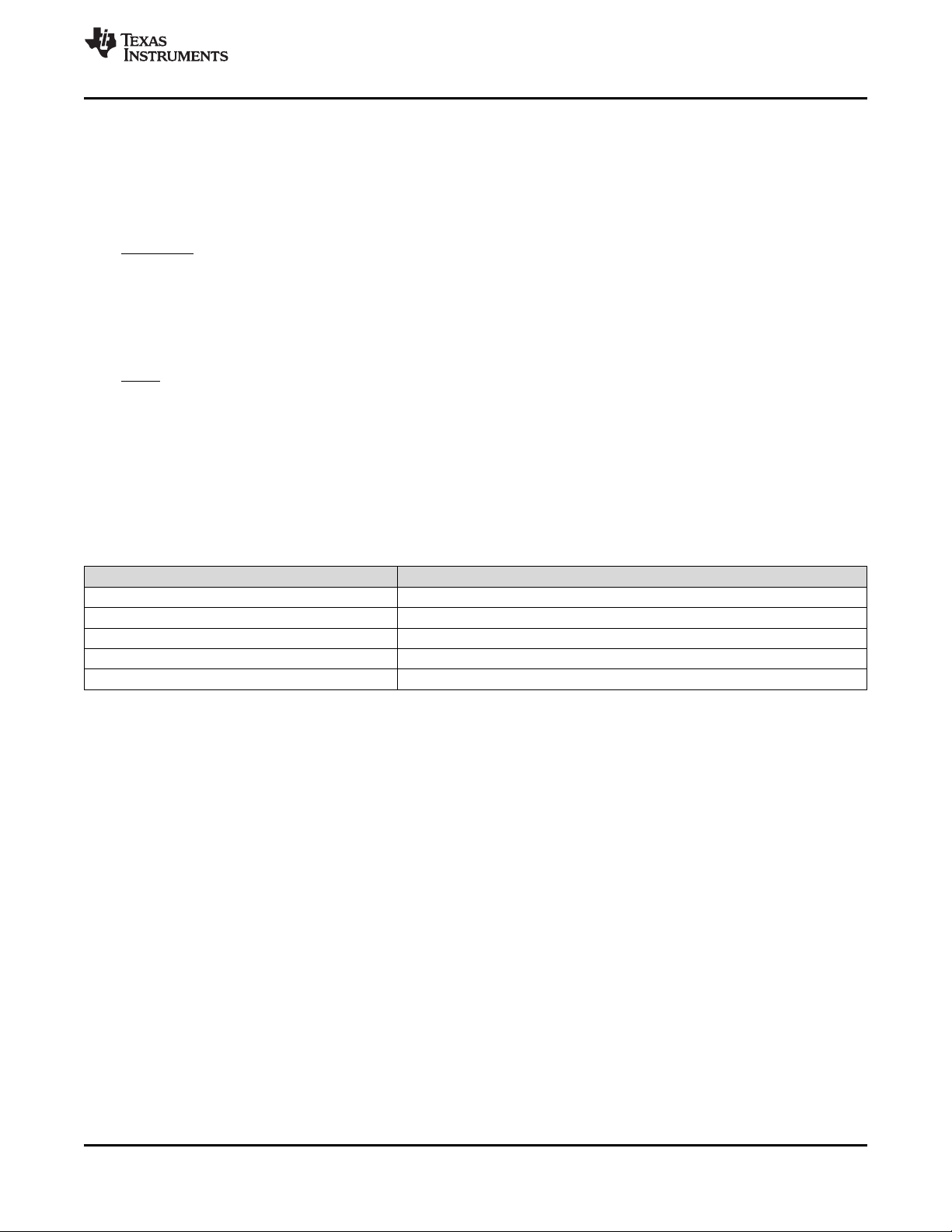
L1
4.7 or 10 µH
V
OUT
C
IN
4.7 µF
LM3670
V
IN
2.5 V to 5.5 V
R
1
R
2
C
OUT
10 µF
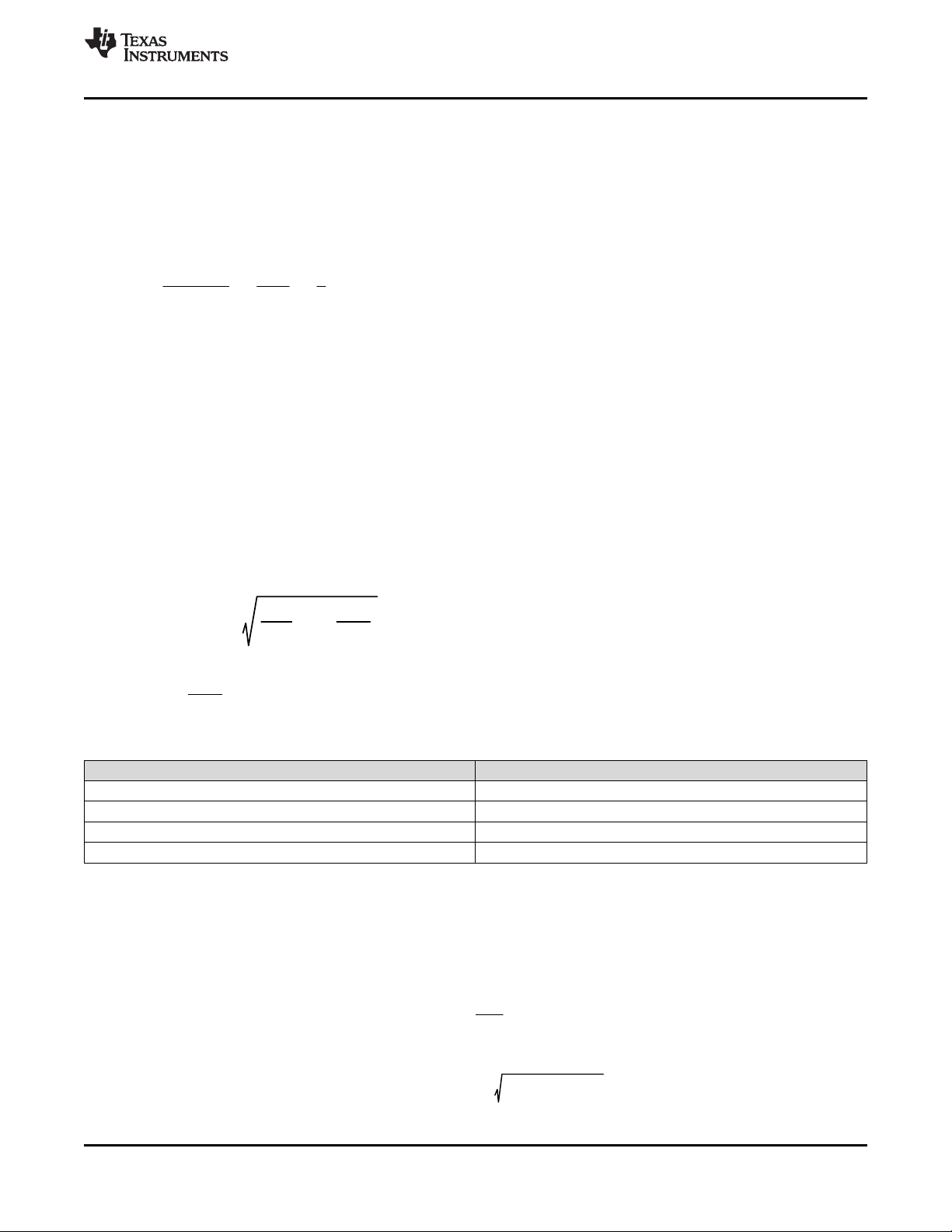
1
2
5
43
V
IN
SW
FB
EN
GND
L1
10 µF
V
OUT
C
IN
4.7 µF
LM3670
V
IN
2.5 V to 5.5 V
C
OUT
10 µF
Product
Folder
Sample &
Buy
Technical
Documents
Tools &
Software
Support &
Community
LM3670
SNVS250F –NOVEMBER 2004–REVISED FEBRUARY 2016
LM3670 Miniature Step-Down DC-DC Converter for Ultralow Voltage Circuits
1 Features
1
• Input Voltage Range: 2.5 V to 5.5 V
• Adjustable Output Voltages (V
): 0.7 V to 2.5 V
OUT
• Fixed Output Voltages: 1.2 V, 1.5 V, 1.6 V, 1.8 V,
1.875 V, 3.3V
• 15-µA Typical Quiescent Current
• 350-mA Maximum Load Capability
• 1-MHz PWM Fixed Switching Frequency (Typical)
• Automatic PFM and PWM Mode Switching
• Low Dropout Operation – 100% Duty Cycle Mode
• Internal Synchronous Rectification for High
Efficiency
• Internal Soft Start
• 0.1-µA Typical Shutdown Current
• Current Overload Protection
• Operates from a Single Li-Ion Cell or Three-Cell
NiMH/NiCd Batteries
• Only Three Tiny Surface-Mount External
Components Required (One Inductor, Two
Ceramic Capacitors)
2 Applications
• Mobile Phones and Handheld Devices
• PDAs
• Palm-Top PCs
• Portable Instruments
• Battery-Powered Devices
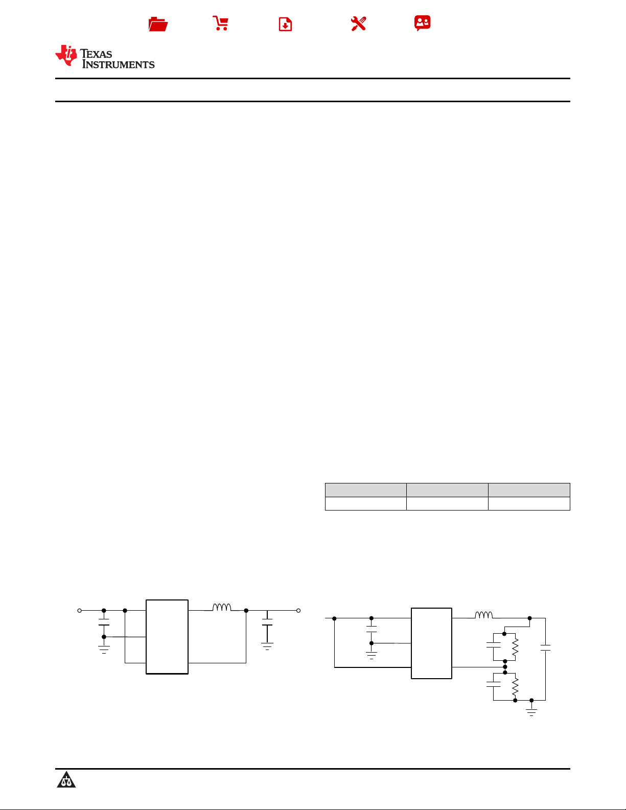
Typical Application: Fixed Output
3 Description
The LM3670 step-down DC-DC converter is
optimized for powering ultralow voltage circuits from a
single Li-Ion cell or three-cell NiMH/NiCd batteries. It
provides up to 350-mA load current, over an input
voltage range from 2.5 V to 5.5 V. There are several
different fixed voltage output options available as well
as an adjustable output voltage version.
The device offers superior features and performance
for mobile phones and similar portable applications
with complex power management systems. Automatic
intelligent switching between pulse width modulation
(PWM) low-noise and pulse frequency modulation
(PFM) low-current mode offers improved system
control. During full-power operation, a fixed-frequency
1-MHz (typical) PWM mode drives loads from
approximately 70 mA to 350 mA maximum, with up to
95% efficiency. Hysteretic PFM mode extends the
battery life through reduction of the quiescent current
to 15 µA (typical) during light current loads and
system standby. Internal synchronous rectification
provides high efficiency (90% to 95% typical at loads
between 1 mA and 100 mA). In shutdown mode
(enable (EN) pin pulled low) the device turns off and
reduces battery consumption to 0.1 µA (typical).
The LM3670 is available in a 5-pin SOT-23 package.
A high switching frequency (1 MHz typical) allows use
of tiny surface-mount components. Only three
external surface-mount components, an inductor and
two ceramic capacitors, are required.
Device Information
PART NUMBER PACKAGE BODY SIZE (NOM)
LM3670 SOT-23 (5) 2.90 mm × 1.60 mm
(1) For all available packages, see the orderable addendum at
the end of the data sheet.
space
space
Typical Application: Adjustable Output Voltage
(1)
1
An IMPORTANT NOTICE at the end of this data sheet addresses availability, warranty, changes, use in safety-critical applications,
intellectual property matters and other important disclaimers. PRODUCTION DATA.
Page 2

LM3670
SNVS250F –NOVEMBER 2004–REVISED FEBRUARY 2016
www.ti.com
Table of Contents
1 Features.................................................................. 1
2 Applications ........................................................... 1
3 Description ............................................................. 1
4 Revision History..................................................... 2
5 Connection Diagram.............................................. 3
6 Specifications......................................................... 4
6.1 Absolute Maximum Ratings...................................... 4
6.2 ESD Ratings.............................................................. 4
6.3 Recommended Operating Conditions....................... 4
6.4 Thermal Information.................................................. 4
6.5 Electrical Characteristics........................................... 5
6.6 Typical Characteristics.............................................. 7
7 Detailed Description............................................ 10
7.1 Overview................................................................. 10
7.2 Functional Block Diagram....................................... 10
7.3 Feature Description................................................. 11
7.4 Device Functional Modes........................................ 12
8 Application and Implementation ........................ 14
8.1 Application Information............................................ 14
8.2 Typical Application ................................................. 14
9 Power Supply Recommendations...................... 18
10 Layout................................................................... 19
10.1 Layout Guidelines ................................................. 19
10.2 Layout Example .................................................... 20
11 Device and Documentation Support ................. 21
11.1 Device Support .................................................... 21
11.2 Community Resources.......................................... 21
11.3 Trademarks........................................................... 21
11.4 Electrostatic Discharge Caution............................ 21
11.5 Glossary................................................................ 21
12 Mechanical, Packaging, and Orderable
Information........................................................... 21
4 Revision History
NOTE: Page numbers for previous revisions may differ from page numbers in the current version.
Changes from Revision E (February 2013) to Revision F Page
• Changed "(0.7V min) to "0.7 V to 2.5 V" ................................................................................................................................ 1
• Added Device Information and Pin Configuration and Functions sections, ESD Ratings and Thermal Information
tables, Feature Description, Device Functional Modes, Application and Implementation, Power Supply
Recommendations, Layout, Device and Documentation Support, and Mechanical, Packaging, and Orderable
Information sections................................................................................................................................................................ 1
• Deleted phone and fax numbers of manufacturers from suggested inductors table ........................................................... 15
• Deleted phone and fax numbers of manufacturers from suggested capacitors table ......................................................... 16
• Deleted rest of text from paragraph beginning "For any output voltages...."........................................................................ 17
• Deleted row beginning with "1.24... "from Table 3 .............................................................................................................. 18
Changes from Revision D (February 2013) to Revision E Page
• Changed layout of National Data Sheet to TI format ........................................................................................................... 19
2
Submit Documentation Feedback Copyright © 2004–2016, Texas Instruments Incorporated
Product Folder Links: LM3670
Page 3
V
IN
1
GND2EN
3
FB
4
SW
5
www.ti.com
5 Connection Diagram
PIN
NUMBE
R
1 V
NAME
IN
2 GND Ground Ground pin.
3 EN Digital Enable input.
4 FB
5 SW Analog
TYPE DESCRIPTION
Power
Analog
Power supply input. Connect to the input filter capacitor
( Typical Application: Fixed Output).
Feedback analog input. Connect to the output filter capacitor
(Typical Application: Fixed Output).
Switching node connection to the internal PFET switch and NFET synchronous rectifier.
Connect to an inductor with a saturation current rating that exceeds the 750-mA maximum
switch peak current limit specification.
LM3670
SNVS250F –NOVEMBER 2004–REVISED FEBRUARY 2016
DBV Package
5-Pin SOT-23
Top View
Pin Functions
Submit Documentation FeedbackCopyright © 2004–2016, Texas Instruments Incorporated
3
Product Folder Links: LM3670
Page 4
LM3670
SNVS250F –NOVEMBER 2004–REVISED FEBRUARY 2016
www.ti.com
6 Specifications
6.1 Absolute Maximum Ratings
over operating free-air temperature range (unless otherwise noted)
VINpin: voltage to GND –0.2 6 V
EN pin: voltage to GND –0.2 6 V
FB, SW pins (GND −0.2) VIN+ 0.2 V
Junction temperature, T
J-MAX
Maximum lead temperature (soldering, 10 seconds) 260 °C
Storage temperature, T
stg
(1) Stresses beyond those listed under Absolute Maximum Ratings may cause permanent damage to the device. These are stress ratings
only, which do not imply functional operation of the device at these or any other conditions beyond those indicated under Recommended
Operating Conditions. Exposure to absolute-maximum-rated conditions for extended periods may affect device reliability.
(2) If Military/Aerospace specified devices are required, contact the TI Sales Office/Distributors for availability and specifications.
6.2 ESD Ratings
Human-body model (HBM), per ANSI/ESDA/JEDEC JS-001
V
(ESD)
(1) JEDEC document JEP155 states that 500-V HBM allows safe manufacturing with a standard ESD control process.
(2) JEDEC document JEP157 states that 250-V CDM allows safe manufacturing with a standard ESD control process.
Electrostatic discharge
Charged-device model (CDM), per JEDEC specification JESD22-
(2)
C101
(1)(2)
MIN MAX UNIT
–45 125 °C
–45 150 °C
VALUE UNIT
(1)
±2000
±200
V
6.3 Recommended Operating Conditions
over operating free-air temperature range (unless otherwise noted)
Input voltage 2.5 5.5 A
Recommended load current 0 350 mA
Junction temperature, T
Ambient temperature, T
(1) All voltages are with respect to the potential at the GND pin.
J
A
(1)
MIN NOM MAX UNIT
–40 125 °C
–40 85 °C
6.4 Thermal Information
LM3670
THERMAL METRIC
R
θJA
R
θJC(top)
R
θJB
ψ
JT
ψ
JB
Junction-to-ambient thermal resistance 163.3 °C/W
Junction-to-case (top) thermal resistance 114.3 °C/W
Junction-to-board thermal resistance 26.8 °C/W
Junction-to-top characterization parameter 12.4 °C/W
Junction-to-board characterization parameter 26.3 °C/W
(1) For more information about traditional and new thermal metrics, see the Semiconductor and IC Package Thermal Metrics application
report, SPRA953.
(1)
UNITDBV (SOT-23)
5 PINS
4
Submit Documentation Feedback Copyright © 2004–2016, Texas Instruments Incorporated
Product Folder Links: LM3670
Page 5
LM3670
www.ti.com
SNVS250F –NOVEMBER 2004–REVISED FEBRUARY 2016
6.5 Electrical Characteristics
Unless otherwise specified, limits for typical values are TJ= 25°C, and minimum and maximum limits apply over the full
operating junction temperature range (−40°C ≤ TJ≤ +125°C); VIN= 3.6 V, V
PARAMETER TEST CONDITIONS MIN TYP MAX UNIT
V
IN
Input voltage See
Fixed output voltage: 1.2 V
Fixed output voltage: 1.5 V
Fixed output voltage: 1.6 V, 1.875 V
V
OUT
Fixed output voltage: 1.8 V
Fixed output voltage: 3.3 V
Adjustable output voltage
(2)
Line_reg Line regulation
Load_reg Load regulation 150 mA ≤ I
V
REF
I
Q_SHDN
I
Q
V
UVLO
R
DSON (P)
R
DSON (N)
I
LKG (P)
I
LKG (N)
I
LIM
Internal reference voltage 0.5 V
Shutdown supply current TA= 85ºC 0.1 1 µA
DC bias current into V
Minimum VINbelow which V
disabled
IN
is
OUT
Pin-pin resistance for PFET VIN= VGS= 3.6V 360 690 mΩ
Pin-pin resistance for NFET VIN= VGS= 3.6 V 250 660 mΩ
P channel leakage current VDS= 5.5 V, TA= 25°C 0.1 1 µA
N channel leakage current VDS= 5.5 V, TA= 25°C 0.1 1.5 µA
Switch peak current limit 400 620 750 mA
(1)
2.5 V ≤ VIN≤ 5.5 V
I
= 10 mA
OUT
2.5 V ≤ VIN≤ 5.5 V
0 mA ≤ I
OUT
≤ 150 mA
2.5 V ≤ VIN≤ 5.5 V
I
= 10 mA
OUT
2.5 V ≤ VIN≤ 5.5 V
0 mA ≤ I
OUT
≤ 350 mA
2.5 V ≤ VIN≤ 5.5 V
I
= 10 mA
OUT
2.5 V ≤ VIN≤ 5.5V
0 mA ≤ I
OUT
≤ 350 mA
2.5 V ≤ VIN≤ 5.5 V
I
= 10 mA
OUT
2.5 V ≤ VIN≤ 5.5 V
0 mA ≤ I
OUT
≤ 350 mA
3.6 V ≤ VIN≤ 5.5 V
I
= 10 mA
OUT
3.6V ≤ VIN≤ 5.5V
0 mA ≤ I
OUT
≤ 350 mA
2.5 V ≤ VIN≤ 5.5 V
I
= 10 mA
OUT
2.5 V ≤ VIN≤ 5.5 V
0 mA ≤ I
OUT
≤ 150 mA
2.5 V ≤ VIN≤ 5.5 V
I
= 10 mA
OUT
≤ 350 mA 0.0014 %/mA
OUT
No load, device is not switching
(V
forced higher than
OUT
programmed output voltage)
TA= −40°C ≤ TJ≤ 125°C 2.4 V
OUT
= 1.8 V, I
–4.5%
–2.5%
–2.5%
–5.5%
–1.5%
–4.5%
–2.5%
= 150 mA, EN = VIN.
OUT
2.5 5.5 V
–2%
4%
4%
4%
–5%
4%
4%
4%
3%
3%
–2%
–6%
4%
4%
4.5%
–4%
4.5%
0.26 %/V
15 30 µA
(1) The input voltage range recommended for the specified output voltages are given below: VIN= 2.5 V to 5.5 V for 0. 7 V ≤ V
V, VIN= ( V
(2) Output voltage specification for the adjustable version includes tolerance of the external resistor divider.
OUT
+ V
DROPOUT
) to 5.5 for 1.875 ≤ V
≤ 3.3 V, where V
OUT
DROPOUT
= I
LOAD
× (R
DSON (P)
+ R
INDUCTOR
).
Submit Documentation FeedbackCopyright © 2004–2016, Texas Instruments Incorporated
Product Folder Links: LM3670
OUT
< 1.875
5
Page 6
LM3670
SNVS250F –NOVEMBER 2004–REVISED FEBRUARY 2016
www.ti.com
Electrical Characteristics (continued)
Unless otherwise specified, limits for typical values are TJ= 25°C, and minimum and maximum limits apply over the full
operating junction temperature range (−40°C ≤ TJ≤ +125°C); VIN= 3.6 V, V
PARAMETER TEST CONDITIONS MIN TYP MAX UNIT
η Efficiency
V
V
I
ƒ
IH
IL
EN
OSC
Logic high input 1.3 V
Logic low input 0.4 V
Enable (EN) input current 0.01 1 µA
Internal oscillator frequency PWM mode 550 1000 1300 kHz
VIN= 3.6 V, V
I
= 1 mA
LOAD
VIN= 3.6 V, V
I
= 10 mA
LOAD
VIN= 3.6 V, V
I
= 100 mA
LOAD
VIN= 3.6 V, V
I
= 200 mA
LOAD
VIN= 3.6 V, V
I
= 300 mA
LOAD
VIN= 3.6 V, V
I
= 350 mA
LOAD
OUT
OUT
OUT
OUT
OUT
OUT
= 1.8 V
= 1.8 V
= 1.8 V
= 1.8 V
= 1.8 V
= 1.8 V
OUT
= 1.8 V, I
= 150 mA, EN = VIN.
OUT
91%
94%
94%
94%
92%
90%
6
Submit Documentation Feedback Copyright © 2004–2016, Texas Instruments Incorporated
Product Folder Links: LM3670
Page 7
I
LOAD
(mA)
40
45
50
55
60
65
70
75
80
85
90
95
100
EFFICIENCY (%)
VIN = 5.0V
VIN = 2.7V
VIN = 3.7V
10
3
10
2
10
1
10
-2
10
-1
10
0
2.5 3 3.5 4 4.5 5 5.5 6
VIN (V)
75
80
85
90
95
100
70
EFFICIENCY (%)
I
LOAD
= 1 mA
I
LOAD
= 300 mA
I
LOAD
= 150 mA
0 50 100 150 200 250 300 350
I
LOAD
(mA)
1.7
1.72
1.74
1.76
1.78
1.8
1.82
1.84
1.86
1.88
1.9
V
OUT
(V)
PFM Mode
PWM Mode
-40
TEMPERATURE (°C)
1.77
1.78
1.79
1.80
1.81
1.82
1.83
V
OUT
(V)
806040200-20
I
OUT
= 10 mA
PFM mode
I
OUT
= 150 mA
PWM mode
VIN = 3.6V
VIN = 2.5V
VIN = 3.6V
VIN = 5.5V
2.5 3 3.5 4 4.5 5 5.5
VIN (V)
10
15
20
NO LOAD I
QUIESCENT
(PA)
TA = 85°C
TA = 25°C
TA = -40°C
-40 -20 0 20 40 60 80
TEMPERATURE (°C)
0
0.05
0.1
I
SHUTDOWN
(PA)
www.ti.com
6.6 Typical Characteristics
Unless otherwise stated, VIN= 3.6 V and V
OUT
LM3670
SNVS250F –NOVEMBER 2004–REVISED FEBRUARY 2016
= 1.8 V.
Figure 1. IQ(Non-Switching) vs V
Figure 3. V
OUT
vs V
IN
IN
Figure 2. IQvs Temperature
Figure 4. V
OUT
vs I
OUT
Figure 5. Efficiency vs I
OUT
Product Folder Links: LM3670
Figure 6. Efficiency vs V
Submit Documentation FeedbackCopyright © 2004–2016, Texas Instruments Incorporated
IN
7
Page 8
V
OUT
(50 mV/Div)
I
LOAD
= 280 mA
TIME (100 Ps/DIV)
CURRENT LOAD STEP (3 mA - 280 mA)
I
LOAD
= 3 mA
V
OUT
(50 mV/Div)
I
LOAD
= 70 mA
TIME (100 Ps/DIV)
CURRENT LOAD STEP (0 mA - 70 mA)
I
LOAD
= 0 mA
Inductor Current = 200 mA/Div
VIN= 3.6V
VIN= 4.6V
TIME (100 ms/DIV)
LINE T
RANSIENT
V
OUT
= 1.8V
(20 mV/Div)
V
OUT
= 1.8V
I
OUT
= 100 mA
VINrisetime= 10 ms
VIN= 3.6V
TIME (200 ms/DIV)
LINE T
RANSIENT
VIN= 2.6V
(20 mV/Div)
2.5 3 3.5 4 4.5 5 5.5
VIN (V)
0.1
0.2
0.3
0.4
0.5
0.6
0.7
0.8
R
DSon
- N, P CHANNEL (:)
N FET
P FET
TA = 85°C
TA = 25°C
TA = -40°C
-40 -20
-10
0 10 20 30 40 50 60 70 80
TEMPERATURE (°C)
840
850
860
870
880
890
900
910
920
930
940
950
960
970
980
990
1000
1010
FREQUENCY (kHz)
-30
I
LOAD
= 150 mA
VIN = 2.5V
VIN = 5.5V
VIN = 3.6V
LM3670
SNVS250F –NOVEMBER 2004–REVISED FEBRUARY 2016
Typical Characteristics (continued)
www.ti.com
Unless otherwise stated, VIN= 3.6 V and V
Figure 7. Frequency vs Temperature
OUT
= 1.8 V.
Figure 8. R
vs. VINP and N Channels
DSON
VIN= 2.6 V to 3.6 V I
8
I
= 3 mA to 280 mA
LOAD
Submit Documentation Feedback Copyright © 2004–2016, Texas Instruments Incorporated
= 100 mA
LOAD
Figure 9. Line Transient
Figure 11. Load Transient
VIN= 3.6 V to 4.6 V I
I
Product Folder Links: LM3670
= 0 mA to 70 mA
LOAD
= 100 mA
LOAD
Figure 10. Line Transient
Figure 12. Load Transient
Page 9
TIME (100 Ps/DIV)
CURRENT LOAD STEP (3 mA - 280 mA)
VIN (2V/Div)
V
OUT
(1V/Div)
(200 mA/
Div)
Inductor
Current
TIME (2 Ps/DIV)
PFM MODE
V
SWITCH
(5V/Div)
V
OUT
(20 mV/Div)
Inductor Current
(100 mA/Div)
TIME (1 Ps/DIV)
PWM MODE
V
SWITCH
(5V/Div)
V
OUT
(20 mV/Div)
Inductor Current
(200 mA/Div)
I
LOAD
= 150 mA
www.ti.com
Typical Characteristics (continued)
LM3670
SNVS250F –NOVEMBER 2004–REVISED FEBRUARY 2016
Unless otherwise stated, VIN= 3.6 V and V
Figure 13. PFM Mode VSW, V
OUT
, I
= 1.8 V.
OUT
INDUCTOR
vs Time Figure 14. PWM Mode VSW, V
OUT
, I
INDUCTOR
vs Time
I
LOAD
= 350 mA
Figure 15. Soft Start VIN, V
Product Folder Links: LM3670
OUT
, I
INDUCTOR
vs Time
Submit Documentation FeedbackCopyright © 2004–2016, Texas Instruments Incorporated
9
Page 10

+
-
+
-
1 MHz
Oscillator
Soft
Start
Ramp
Generator
+
-
+
-
Thermal
Shutdown
Undervoltage
Lockout
V
REF
+
-
0.5V
Error
Amp
Control Logic Driver
Current Limit
Comparator
Ref1
PFM Current
Comparator
Ref2
SW
Zero Crossing
Comparator
FB
EN
V
IN
PWM Comparator
pfm_low
pfm_hi
GND
Bandgap
+
-
Vcomp
1.0V
Frequency
Compensation
Adj Version
Fixed Version
LM3670
SNVS250F –NOVEMBER 2004–REVISED FEBRUARY 2016
www.ti.com
7 Detailed Description
7.1 Overview
The LM3670, a high-efficiency step-down DC-DC switching buck converter, delivers a constant voltage from
either a single Li-Ion or three-cell NiMH/NiCd battery to portable devices such as cell phones and PDAs. Using a
voltage mode architecture with synchronous rectification, the LM3670 can deliver up to 350 mA depending on the
input voltage and output voltage (voltage head room), and the inductor chosen (maximum current capability).
There are three modes of operation depending on the current required: pulse width modulation (PWM), pulse
frequency modulation (PFM), and shutdown. PWM mode handles current loads of approximately 70 mA or
higher. Lighter output current loads cause the device to automatically switch into PFM for reduced current
consumption (IQ= 15 µA typical) and a longer battery life. Shutdown mode turns off the device, offering the
lowest current consumption (I
SHUTDOWN
The LM3670 can operate up to a 100% duty cycle (PMOS switch always on) for low dropout control of the output
voltage. In this way the output voltage is controlled down to the lowest possible input voltage.
Additional features include soft-start, undervoltage lockout, current overload protection, and thermal overload
protection. As shown in Figure 17, only three external power components are required for implementation.
7.2 Functional Block Diagram
= 0.1 µA typical).
10
Submit Documentation Feedback Copyright © 2004–2016, Texas Instruments Incorporated
Product Folder Links: LM3670
Page 11
-V
OUT
VIN-V
OUT
LM3670
www.ti.com
SNVS250F –NOVEMBER 2004–REVISED FEBRUARY 2016
7.3 Feature Description
7.3.1 Circuit Operation
The LM3670 operates as follows. During the first portion of each switching cycle, the control block in the LM3670
turns on the internal PFET switch. This allows current to flow from the input through the inductor to the output
filter capacitor and load. The inductor limits the current to a ramp with a slope of:
(1)
by storing energy in a magnetic field. During the second portion of each cycle, the controller turns the PFET
switch off, blocking current flow from the input, and then turns the NFET synchronous rectifier on. The inductor
draws current from ground through the NFET to the output filter capacitor and load, which ramps the inductor
current down with a slope of:
(2)
The output filter stores charge when the inductor current is high, and releases it when low, smoothing the voltage
across the load.
7.3.2 Soft Start
The LM3670 has a soft-start circuit that limits in-rush current during start-up. Typical start-up times with a 10-µF
output capacitor and 350-mA load is 400 µs:
Table 1. Typical Start-Up Times for Soft Start
INRUSH CURRENT (mA) DURATION (µs)
0 32
70 224
140 256
280 256
620 until soft start ends
7.3.3 LDO - Low Dropout Operation
The LM3670 can operate at 100% duty cycle (no switching, PMOS switch is completely on) for low dropout
support of the output voltage. In this way the output voltage is controlled down to the lowest possible input
voltage.
The minimum input voltage needed to support the output voltage is
V
IN_MIN
= I
LOAD
× (R
DSON,PFET
+ R
INDUCTOR
) + V
OUT
where
• I
• R
• R
= load current
LOAD
DSON, PFET
INDUCTOR
= the drain to source resistance of PFET switch in the triode region
= the inductor resistance (3)
Submit Documentation FeedbackCopyright © 2004–2016, Texas Instruments Incorporated
Product Folder Links: LM3670
11
Page 12

PFM Peak
=
V
IN
64:
117 mA +
(typ)
MODE
<
V
IN
50:
26 mA +
(typ)
LM3670
SNVS250F –NOVEMBER 2004–REVISED FEBRUARY 2016
www.ti.com
7.4 Device Functional Modes
7.4.1 PWM Operation
During PWM operation the converter operates as a voltage-mode controller with input voltage feed forward. This
allows the converter to achieve excellent load and line regulation. The DC gain of the power stage is proportional
to the input voltage. To eliminate this dependence, feed forward inversely proportional to the input voltage is
introduced.
7.4.1.1 Internal Synchronous Rectification
While in PWM mode, the LM3670 uses an internal NFET as a synchronous rectifier to reduce rectifier forward
voltage drop and associated power loss. Synchronous rectification provides a significant improvement in
efficiency whenever the output voltage is relatively low compared to the voltage drop across an ordinary rectifier
diode.
7.4.1.2 Current Limiting
A current limit feature allows the LM3670 to protect itself and external components during overload conditions
PWM mode implements cycle-by-cycle current limiting using an internal comparator that trips at 620 mA (typical).
7.4.2 PFM Operation
At very light load, the converter enters PFM mode and operates with reduced switching frequency and supply
current to maintain high efficiency.
The part automatically transition into PFM mode when either of two conditions occurs for a duration of 32 or
more clock cycles:
1. The inductor current becomes discontinuous
2. The peak PMOS switch current drops below the I
MODE
level:
(4)
During PFM operation, the converter positions the output voltage slightly higher than the nominal output voltage
in PWM operation, allowing additional headroom for voltage drop during a load transient from light to heavy load.
The PFM comparator senses the output voltage via the feedback pin and control the switching of the output
FETs such that the output voltage ramps between 0.8% and 1.6% (typical) above the nominal PWM output
voltage. If the output voltage is below the high PFM comparator threshold, the PMOS power switch is turned on.
It remains on until the output voltage exceeds the ‘high’ PFM threshold or the peak current exceeds the I
PFM
level
set for PFM mode. The peak current in PFM mode is:
(5)
Once the PMOS power switch is turned off, the NMOS power switch is turned on until the inductor current ramps
to zero. When the NMOS zero-current condition is detected, the NMOS power switch is turned off. If the output
voltage is below the high PFM comparator threshold (see Figure 16), the PMOS switch is again turned on and
the cycle is repeated until the output reaches the desired level. Once the output reaches the high PFM threshold,
the NMOS switch is turned on briefly to ramp the inductor current to zero and then both output switches are
turned off and the part enters an extremely low power mode. Quiescent supply current during this sleep mode is
less than 30 µA, which allows the part to achieve high efficiencies under extremely light load conditions. When
the output drops below the low PFM threshold, the cycle repeats to restore the output voltage to approximately
1.6% above the nominal PWM output voltage.
If the load current increases during PFM mode (see Figure 16) causing the output voltage to fall below the ‘low2’
PFM threshold, the part automatically transitions into fixed-frequency PWM mode.
12
Submit Documentation Feedback Copyright © 2004–2016, Texas Instruments Incorporated
Product Folder Links: LM3670
Page 13

High PFM Threshold
~1.016 × V
OUT
Low1 PFM Threshold
~1.008 × V
OUT
PFM Mode at Light Load
PWM Mode at
Moderateto-Heavy
Loads
Pfet on
until
Ipfm limit
reached
Nfet on
drains
inductor
current
until
I inductor = 0
High PFM
Voltage
Threshold
reached,
go into
sleep mode
Low PFM
Threshold,
turn on
PFET
Current load
increases,
draws VOUT
towards
Low2 PFM
Threshold
Low2 PFM Threshold,
switch back to PWM mode
Load current
increases
Low2 PFM Threshold
V
OUT
Z-
Ax
is
Z
-
Axis
www.ti.com
Device Functional Modes (continued)
Figure 16. Operation in PFM Mode and Transition to PWM Mode
LM3670
SNVS250F –NOVEMBER 2004–REVISED FEBRUARY 2016
7.4.3 Shutdown
Setting the EN input pin low (< 0.4 V) places the LM3670 in shutdown mode. During shutdown the PFET switch,
NFET switch, reference, control and bias circuitry of the LM3671 are turned off. Setting EN high (> 1.3 V)
enables normal operation. It is recommended to set EN pin low to turn off the LM3671 during system power up
and undervoltage conditions when the supply is less than 2.5 V. Do not leave the EN pin floating.
Product Folder Links: LM3670
Submit Documentation FeedbackCopyright © 2004–2016, Texas Instruments Incorporated
13
Page 14

V
OUT
=
VIN-V
OUT
2 L
I
LOAD
+
(
)
V
OUT
V
IN
(
)
(
1
f
)
MAX
=
I
RIPPLE
I
LOAD
+
1
2
5
43
V
IN
SW
FB
EN
GND
L1
10 µF
V
OUT
C
IN
4.7 µF
LM3670
V
IN
2.5 V to 5.5 V
C
OUT
10 µF
LM3670
SNVS250F –NOVEMBER 2004–REVISED FEBRUARY 2016
www.ti.com
8 Application and Implementation
NOTE
Information in the following applications sections is not part of the TI component
specification, and TI does not warrant its accuracy or completeness. TI’s customers are
responsible for determining suitability of components for their purposes. Customers should
validate and test their design implementation to confirm system functionality.
8.1 Application Information
The external control of this device is very easy. First make sure the correct voltage been applied at VINpin, then
simply apply the voltage at EN pin according to the Electrical Characteristics to enable or disable the output
voltage.
8.2 Typical Application
8.2.1 Typical Application: Fixed Output
Figure 17. LM3670 Typical Application, Fixed Output
8.2.1.1 Design Requirements
For typical CMOS voltage regulator applications, use the parameters listed in Table 2.
Table 2. Design Parameters
DESIGN PARAMETER EXAMPLE VALUE
Minimum input voltage 2.5 V
Minimum output voltage 1.2 V
Maximum load current 350 mA
8.2.1.2 Detailed Design Procedure
8.2.1.2.1 Inductor Selection
There are two main considerations when choosing an inductor: the inductor current must not saturate, and the
inductor current ripple is small enough to achieve the desired output voltage ripple.
There are two methods to choose the inductor current rating.
8.2.1.2.1.1 Method 1
The total current is the sum of the load and the inductor ripple current. This can be written as
(6)
where
• I
LOAD
• VIN= input voltage
14
Submit Documentation Feedback Copyright © 2004–2016, Texas Instruments Incorporated
= load current
Product Folder Links: LM3670
Page 15
V
PP-RMS
= V
PP-C
2
+ V
PP-ESR
2
V
OUT
=
V
PP-ESR
= IPP * R
ESR
V
PP-C
=
f*8*C
I
PP
I
RMS OUTMAX
*
* (1 -
)
V
OUT
V
IN
V
OUT
V
IN
= I
The worst case IRMS is:
=
2
IRMS
IRMS
(duty cycle = 50%)
) * (
1
f
)) * (L >= (
VIN - V
OUT
I
PP
V
OUT
V
IN
LM3670
www.ti.com
• L = inductor
• ƒ = switching frequency
• I
RIPPLE
8.2.1.2.1.2 Method 2
= peak-to-peak current (7)
SNVS250F –NOVEMBER 2004–REVISED FEBRUARY 2016
A more conservative approach is to choose an inductor that can handle the current limit of 700 mA.
Given a peak-to-peak current ripple (IPP) the inductor needs to be at least
(8)
A 10-µH inductor with a saturation current rating of at least 800 mA is recommended for most applications.
Resistance of the inductor resistance must be less than around 0.3 Ω for good efficiency. Table 3 lists suggested
inductors and suppliers. For low-cost applications, an unshielded bobbin inductor is suggested. For noise critical
applications, a toroidal or shielded-bobbin inductor must be used. A good practice is to lay out the board with
overlapping footprints of both types for design flexibility. This allows substitution of a low-noise toroidal inductor,
in the event that noise from low-cost bobbin models is unacceptable.
8.2.1.2.2 Input Capacitor Selection
A ceramic input capacitor of 4.7 µF is sufficient for most applications. A larger value may be used for improved
input voltage filtering. The input filter capacitor supplies current to the PFET switch of the LM3670 in the first half
of each cycle and reduces voltage ripple imposed on the input power source. The low equivalent series
resistance (ESR) of a ceramic capacitor provides the best noise filtering of the input voltage spikes due to this
rapidly changing current. Select an input filter capacitor with a surge current rating sufficient for the power-up
surge from the input power source. The power-up surge current is approximately the value of the capacitor (µF)
times the voltage rise rate (V/µs). The input current ripple can be calculated by :
8.2.1.2.3 Output Capacitor Selection
The output filter capacitor smooths out current flow from the inductor to the load, maintaining a steady output
voltage during transient load changes and reduces output voltage ripple. These capacitors must be selected with
sufficient capacitance and sufficiently low ESR to perform these functions.
The output ripple current can be calculated as:
Voltage peak-to-peak ripple due to capacitance =
Voltage peak-to-peak ripple due to ESR =
Voltage peak-to-peak ripple, root mean squared =
Table 3. Suggested Inductors and Their Suppliers
MODEL VENDOR
IDC2512NB100M Vishay
DO1608C-103 Coilcraft
ELL6RH100M Panasonic
CDRH5D18-100 Sumida
Product Folder Links: LM3670
Submit Documentation FeedbackCopyright © 2004–2016, Texas Instruments Incorporated
(9)
15
Page 16
V
OUT
(50 mV/Div)
I
LOAD
= 0 mA
TIME (100 Ps/DIV)
CURRENT LOAD STEP (0 mA - 280 mA)
I
LOAD
= 280 mA
V
OUT
(50 mV/Div)
I
LOAD
= 350 mA
TIME (100 Ps/DIV)
CURRENT LOAD STEP (0 mA - 350 mA)
I
LOAD
= 0 mA
LM3670
SNVS250F –NOVEMBER 2004–REVISED FEBRUARY 2016
www.ti.com
Note that the output ripple is dependent on the current ripple and the equivalent series resistance of the output
capacitor (R
Because these two components are out-of-phase the RMS value is used. The R
well as temperature dependent); make sure the frequency of the R
ESR
).
is frequency dependent (as
given is the same order of magnitude as
ESR
ESR
the switching frequency.
Table 4. Suggested Capacitors And Their Suppliers
MODEL TYPE VENDOR
10 µF for C
OUT
VJ1812V106MXJAT Ceramic Vishay
LMK432BJ106MM Ceramic Taiyo-Yuden
JMK325BJ106MM Ceramic Taiyo-Yuden
4.7 µF for C
IN
VJ1812V475MXJAT Ceramic Vishay
EMK325BJ475MN Ceramic Taiyo-Yuden
C3216X5R0J475M Ceramic TDK
8.2.1.3 Application Curves
I
= 0 mA to 280 mA
LOAD
Figure 18. Load Transient
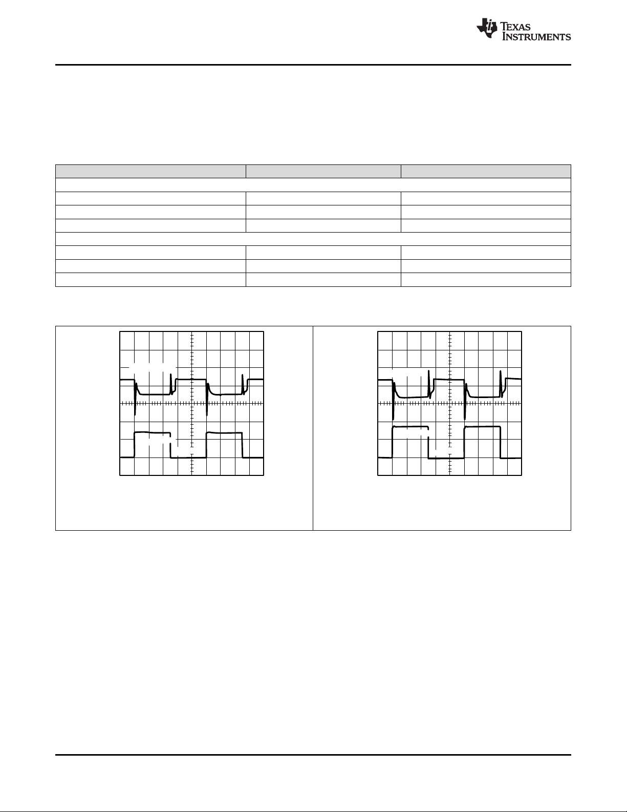
16
Submit Documentation Feedback Copyright © 2004–2016, Texas Instruments Incorporated
I
= 0 mA to 350 mA
LOAD
Figure 19. Load Transient
Product Folder Links: LM3670
Page 17

1
=
1
2 S R1 10 kHz
V
OUT
=
R
1
R
VFB *
+ 1
( )
1
2
5
4
3
V
IN
SW
FB
EN
GND
L1
4.7 or 10 µH
V
OUT
C
IN
4.7 µF
LM3670
V
IN
2.5 V to 5.5 V
R
1
R
2
C
OUT
10 µF
www.ti.com
8.2.2 Typical Application: Adjustable Output
Figure 20. LM3670 Typical Application: Adjustable Output
8.2.2.1 Design Requirements
For adjustable LM3670 option, use the design parameters in Table 5
Table 5. Design Parameters
DESIGN PARAMETER EXAMPLE VALUE
Input voltage range 2.5 V to 5.5
Input capacitor 4.7 µF
Output capacitor 10 µF
Inductor 4.7 µH or 10 µH
ADJ programmable output voltage 0.7 V to 2.5 V
LM3670
SNVS250F –NOVEMBER 2004–REVISED FEBRUARY 2016
8.2.2.2 Detailed Design Procedure
8.2.2.2.1 Output Voltage Selection for Adjustable LM3670
The output voltage of the adjustable parts can be programmed through the resistor network connected from V
to VFBthen to GND. V
is adjusted to make VFBequal to 0.5 V. The resistor from VFBto GND (R2) must be at
OUT
OUT
least 100 KΩ to keep the current sunk through this network well below the 15-µA quiescent current level (PFM
mode with no switching) but large enough that it is not susceptible to noise. If R2is 200 KΩ, and VFBis 0.5 V,
then the current through the resistor feedback network is 2.5 µA (IFB= 0.5 V / R2). The output voltage formula is:
where
• V
• VFB= feedback voltage (0.5 V typical)
• R1Resistor from V
• R2Resistor from V
= output voltage (V)
OUT
to VFB(Ω)
OUT
to GND (Ω) (10)
OUT
For output voltage greater than or equal to 0.7 V a frequency zero must be added at 10 kHz for stability.
(11)
For any output voltages equal to 0.7 V or 2.5 V, a pole must also be placed at 10 kHz (see Table 6).
Submit Documentation FeedbackCopyright © 2004–2016, Texas Instruments Incorporated
Product Folder Links: LM3670
17
Page 18
V
OUT
(50 mV/Div)
I
LOAD
= 50 mA
TIME (100 Ps/DIV)
CURRENT LOAD STEP (50 mA - 350 mA)
I
LOAD
= 350 mA
V
OUT
(50 mV/Div)
I
LOAD
= 300 mA
TIME (100 ms/DIV)
CURREN
T LOAD ST
EP (100 mA
- 300 mA)
I
LOAD
=100mA
Inductor Current = 200 mA/Div
LM3670
SNVS250F –NOVEMBER 2004–REVISED FEBRUARY 2016
www.ti.com
Table 6. Adjustable LM3670 Configurations for Various V
OUT
VOUT (V) R1 (KΩ) R2 (KΩ) C1 (pF) C2 (pF) L (µH) CIN(µF) C
0.7 80.6 200 200 150 4.7 4.7 10
0.8 120 200 130 none 4.7 4.7 10
0.9 160 200 100 none 4.7 4.7 10
1.0 200 200 82 none 4.7 4.7 10
1.1 240 200 68 none 4.7 4.7 10
1.2 280 200 56 none 4.7 4.7 10
1.24 221 150 75 120 4.7 4.7 10
1.5 402 200 39 none 10 4.7 10
1.6 442 200 39 none 10 4.7 10
1.7 487 200 33 none 10 4.7 10
1.875 549 200 30 none 10 4.7 14.7
2.5 806 200 22 82 10 4.7 22
(1) (10 || 4.7)
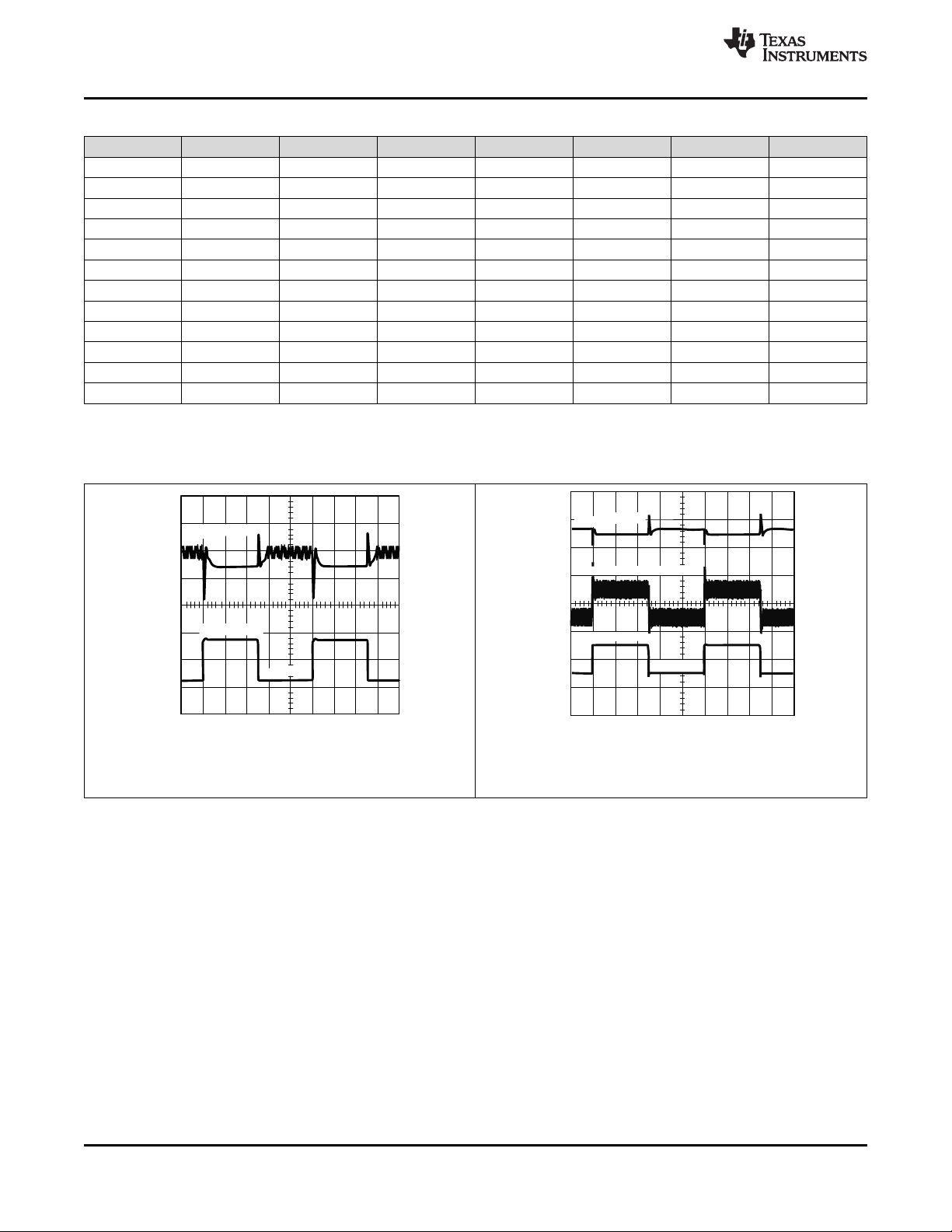
8.2.2.3 Application Curves
OUT
(µF)
(1)
9 Power Supply Recommendations
The LM3670 is designed to operate from a stable input supply range of 2.5 V to 5.5 V.
18
I
I
= 50 mA to 350 mA
LOAD
Figure 21. Load Transient
Submit Documentation Feedback Copyright © 2004–2016, Texas Instruments Incorporated
= 100 mA to 300 mA
LOAD
Figure 22. Load Transient
Product Folder Links: LM3670
Page 19

LM3670
www.ti.com
SNVS250F –NOVEMBER 2004–REVISED FEBRUARY 2016
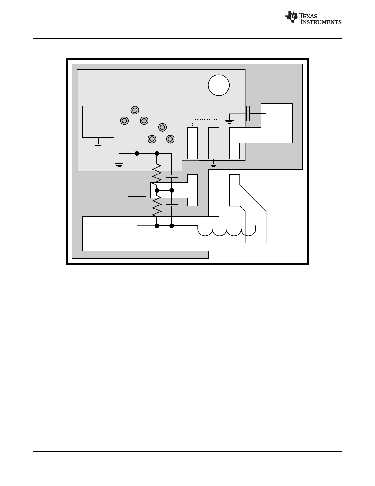
10 Layout
10.1 Layout Guidelines
PC board layout is an important part of DC-DC converter design. Poor board layout can disrupt the performance
of a DC-DC converter and surrounding circuitry by contributing to EMI, ground bounce, and resistive voltage loss
in the traces, which can send erroneous signals to the DC-DC converter device, resulting in poor regulation or
instability.
Good layout for the LM3670 can be implemented by following a few simple design rules, as shown in Figure 23.
• Place the LM3670, inductor and filter capacitors close together and make the traces short. The traces
between these components carry relatively high switching currents and act as antennas. Following this rule
reduces radiated noise. Place the capacitors and inductor within 0.2 in. (5 mm) of the LM3670.
• Arrange the components so that the switching current loops curl in the same direction. During the first half of
each cycle, current flows from the input filter capacitor, through the LM3670 and inductor to the output filter
capacitor and back through ground, forming a current loop. In the second half of each cycle, current is pulled
up from ground, through the LM3670 by the inductor, to the output filter capacitor and then back through
ground, forming a second current loop. Routing these loops so the current curls in the same direction
prevents magnetic field reversal between the two half-cycles and reduces radiated noise.
• Connect the ground pins of the LM3670, and filter capacitors together using generous component-side copper
fill as a pseudo-ground plane. Then, connect this to the ground-plane (if one is used) with several vias. This
reduces ground-plane noise by preventing the switching currents from circulating through the ground plane. It
also reduces ground bounce at the LM3670 by giving it a low-impedance ground connection.
• Use wide traces between the power components and for power connections to the DC-DC converter circuit.
This reduces voltage errors caused by resistive losses across the traces.
• Route noise sensitive traces, such as the voltage feedback path, away from noisy traces between the power
components. The voltage feedback trace must remain close to the LM3670 circuit, and be direct but must be
routed opposite to noisy components. This reduces EMI radiated onto the DC-DC converter’s own voltage
feedback trace.
• Place noise sensitive circuitry, such as radio IF blocks, away from the DC-DC converter, CMOS digital blocks
and other noisy circuitry. Interference with noise-sensitive circuitry in the system can be reduced through
distance.
In mobile phones, for example, a common practice is to place the DC-DC converter on one corner of the board,
arrange the CMOS digital circuitry around it (because this also generates noise), and then place sensitive preamplifiers and IF stages on the diagonally opposing corner. Often, the sensitive circuitry is shielded with a metal
pan and, by using low-dropout linear regulators, power to the circuit is post-regulated to reduce conducted noise.
Product Folder Links: LM3670
Submit Documentation FeedbackCopyright © 2004–2016, Texas Instruments Incorporated
19
Page 20
EN
G
ND
S
W
GND
EN
POST
PIN
The light shaded area is the top surface ground. C , C , Feedback R
and C grounds all come to this area which is as far away from the SW pin
as possible to avoid the noise created at the SW pin.
Note that the top and bottom GND sides are kept away from the SW pin to
avoid picking up noise from the SW pin which swings from GND to V .
OUT IN
IN
EN post pin is connected to EN with a bottom side trace to
maintain unbroken ground plane on top of board
C
OUT
C
IN
R1_fb
C1_fb
R2_fb
C2_fb
L1
EN,GND,V ,FB,SW are
the pads for the SOT-23-5
package
IN
FB
As many through holes
as possible here to
connect the top and
bottom ground planes
V
IN
S
W
V
OUT
The V , SW, V traces,
C , C traces & pads
should be thick - they are
high current paths
IN OUT
IN OUT
Bottom surface - the darker
shaded area is all GND EXCEPT
for area around SW to avoid
picking up switch noise.
If possible put the feedback Rs and Cs on the back side so the C
GND can move closer to the IC GND
OUT
SW node is switching
between V and GND at
1 MHz - VERY NOISY! -
keep all GNDs and GND
planes away!
IN
LM3670
SNVS250F –NOVEMBER 2004–REVISED FEBRUARY 2016
10.2 Layout Example
www.ti.com
20
Submit Documentation Feedback Copyright © 2004–2016, Texas Instruments Incorporated
Figure 23. LM3670 Layout
Product Folder Links: LM3670
Page 21
LM3670
www.ti.com
SNVS250F –NOVEMBER 2004–REVISED FEBRUARY 2016
11 Device and Documentation Support
11.1 Device Support
11.1.1 Third-Party Products Disclaimer
TI'S PUBLICATION OF INFORMATION REGARDING THIRD-PARTY PRODUCTS OR SERVICES DOES NOT
CONSTITUTE AN ENDORSEMENT REGARDING THE SUITABILITY OF SUCH PRODUCTS OR SERVICES
OR A WARRANTY, REPRESENTATION OR ENDORSEMENT OF SUCH PRODUCTS OR SERVICES, EITHER
ALONE OR IN COMBINATION WITH ANY TI PRODUCT OR SERVICE.
11.2 Community Resources
The following links connect to TI community resources. Linked contents are provided "AS IS" by the respective
contributors. They do not constitute TI specifications and do not necessarily reflect TI's views; see TI's Terms of
Use.
TI E2E™ Online Community TI's Engineer-to-Engineer (E2E) Community. Created to foster collaboration
among engineers. At e2e.ti.com, you can ask questions, share knowledge, explore ideas and help
solve problems with fellow engineers.
Design Support TI's Design Support Quickly find helpful E2E forums along with design support tools and
contact information for technical support.
11.3 Trademarks
E2E is a trademark of Texas Instruments.
All other trademarks are the property of their respective owners.
11.4 Electrostatic Discharge Caution
These devices have limited built-in ESD protection. The leads should be shorted together or the device placed in conductive foam
during storage or handling to prevent electrostatic damage to the MOS gates.
11.5 Glossary
SLYZ022 — TI Glossary.
This glossary lists and explains terms, acronyms, and definitions.
12 Mechanical, Packaging, and Orderable Information
The following pages include mechanical, packaging, and orderable information. This information is the most
current data available for the designated devices. This data is subject to change without notice and revision of
this document. For browser-based versions of this data sheet, refer to the left-hand navigation.
Product Folder Links: LM3670
Submit Documentation FeedbackCopyright © 2004–2016, Texas Instruments Incorporated
21
Page 22

PACKAGE OPTION ADDENDUM
www.ti.com
PACKAGING INFORMATION
Orderable Device Status
LM3670MF-1.2/NOPB ACTIVE SOT-23 DBV 5 1000 Green (RoHS
LM3670MF-1.5/NOPB ACTIVE SOT-23 DBV 5 1000 Green (RoHS
LM3670MF-1.6/NOPB ACTIVE SOT-23 DBV 5 1000 Green (RoHS
LM3670MF-1.8 NRND SOT-23 DBV 5 TBD Call TI Call TI -40 to 85 SDCB
LM3670MF-1.8/NOPB ACTIVE SOT-23 DBV 5 1000 Green (RoHS
LM3670MF-1.875/NOPB ACTIVE SOT-23 DBV 5 1000 Green (RoHS
LM3670MF-3.3 NRND SOT-23 DBV 5 1000 TBD Call TI Call TI -40 to 85 SDEB
LM3670MF-3.3/NOPB ACTIVE SOT-23 DBV 5 1000 Green (RoHS
LM3670MF-ADJ/NOPB ACTIVE SOT-23 DBV 5 1000 Green (RoHS
LM3670MFX-1.2/NOPB ACTIVE SOT-23 DBV 5 3000 Green (RoHS
LM3670MFX-1.8/NOPB ACTIVE SOT-23 DBV 5 3000 Green (RoHS
LM3670MFX-ADJ/NOPB ACTIVE SOT-23 DBV 5 3000 Green (RoHS
(1)
The marketing status values are defined as follows:
ACTIVE: Product device recommended for new designs.
LIFEBUY: TI has announced that the device will be discontinued, and a lifetime-buy period is in effect.
NRND: Not recommended for new designs. Device is in production to support existing customers, but TI does not recommend using this part in a new design.
PREVIEW: Device has been announced but is not in production. Samples may or may not be available.
OBSOLETE: TI has discontinued the production of the device.
Package Type Package
(1)
Drawing
Pins Package
Qty
Eco Plan
(2)
& no Sb/Br)
& no Sb/Br)
& no Sb/Br)
& no Sb/Br)
& no Sb/Br)
& no Sb/Br)
& no Sb/Br)
& no Sb/Br)
& no Sb/Br)
& no Sb/Br)
Lead/Ball Finish
(6)
MSL Peak Temp
(3)
Op Temp (°C) Device Marking
CU SN Level-1-260C-UNLIM -40 to 85 SCZB
CU SN Level-1-260C-UNLIM -40 to 85 S82B
CU SN Level-1-260C-UNLIM -40 to 85 SDBB
CU SN Level-1-260C-UNLIM -40 to 85 SDCB
CU SN Level-1-260C-UNLIM -40 to 85 SEFB
CU SN Level-1-260C-UNLIM -40 to 85 SDEB
CU SN Level-1-260C-UNLIM -40 to 85 SDFB
CU SN Level-1-260C-UNLIM -40 to 85 SCZB
CU SN Level-1-260C-UNLIM -40 to 85 SDCB
CU SN Level-1-260C-UNLIM -40 to 85 SDFB
(4/5)
(2)
Eco Plan - The planned eco-friendly classification: Pb-Free (RoHS), Pb-Free (RoHS Exempt), or Green (RoHS & no Sb/Br) - please check http://www.ti.com/productcontent for the latest availability
information and additional product content details.
TBD: The Pb-Free/Green conversion plan has not been defined.
Pb-Free (RoHS): TI's terms "Lead-Free" or "Pb-Free" mean semiconductor products that are compatible with the current RoHS requirements for all 6 substances, including the requirement that
lead not exceed 0.1% by weight in homogeneous materials. Where designed to be soldered at high temperatures, TI Pb-Free products are suitable for use in specified lead-free processes.
7-Jan-2016
Samples
Addendum-Page 1
Page 23

PACKAGE OPTION ADDENDUM
www.ti.com
Pb-Free (RoHS Exempt): This component has a RoHS exemption for either 1) lead-based flip-chip solder bumps used between the die and package, or 2) lead-based die adhesive used between
the die and leadframe. The component is otherwise considered Pb-Free (RoHS compatible) as defined above.
Green (RoHS & no Sb/Br): TI defines "Green" to mean Pb-Free (RoHS compatible), and free of Bromine (Br) and Antimony (Sb) based flame retardants (Br or Sb do not exceed 0.1% by weight
in homogeneous material)
(3)
MSL, Peak Temp. - The Moisture Sensitivity Level rating according to the JEDEC industry standard classifications, and peak solder temperature.
(4)
There may be additional marking, which relates to the logo, the lot trace code information, or the environmental category on the device.
(5)
Multiple Device Markings will be inside parentheses. Only one Device Marking contained in parentheses and separated by a "~" will appear on a device. If a line is indented then it is a continuation
of the previous line and the two combined represent the entire Device Marking for that device.
(6)
Lead/Ball Finish - Orderable Devices may have multiple material finish options. Finish options are separated by a vertical ruled line. Lead/Ball Finish values may wrap to two lines if the finish
value exceeds the maximum column width.
Important Information and Disclaimer:The information provided on this page represents TI's knowledge and belief as of the date that it is provided. TI bases its knowledge and belief on information
provided by third parties, and makes no representation or warranty as to the accuracy of such information. Efforts are underway to better integrate information from third parties. TI has taken and
continues to take reasonable steps to provide representative and accurate information but may not have conducted destructive testing or chemical analysis on incoming materials and chemicals.
TI and TI suppliers consider certain information to be proprietary, and thus CAS numbers and other limited information may not be available for release.
In no event shall TI's liability arising out of such information exceed the total purchase price of the TI part(s) at issue in this document sold by TI to Customer on an annual basis.
7-Jan-2016
Addendum-Page 2
Page 24

PACKAGE MATERIALS INFORMATION
www.ti.com 8-Jan-2016
TAPE AND REEL INFORMATION
*All dimensions are nominal
Device Package
Type
LM3670MF-1.2/NOPB SOT-23 DBV 5 1000 178.0 8.4 3.2 3.2 1.4 4.0 8.0 Q3
LM3670MF-1.5/NOPB SOT-23 DBV 5 1000 178.0 8.4 3.2 3.2 1.4 4.0 8.0 Q3
LM3670MF-1.6/NOPB SOT-23 DBV 5 1000 178.0 8.4 3.2 3.2 1.4 4.0 8.0 Q3
LM3670MF-1.8/NOPB SOT-23 DBV 5 1000 178.0 8.4 3.2 3.2 1.4 4.0 8.0 Q3
LM3670MF-1.875/NOPB SOT-23 DBV 5 1000 178.0 8.4 3.2 3.2 1.4 4.0 8.0 Q3
LM3670MF-3.3 SOT-23 DBV 5 1000 178.0 8.4 3.2 3.2 1.4 4.0 8.0 Q3
LM3670MF-3.3/NOPB SOT-23 DBV 5 1000 178.0 8.4 3.2 3.2 1.4 4.0 8.0 Q3
LM3670MF-ADJ/NOPB SOT-23 DBV 5 1000 178.0 8.4 3.2 3.2 1.4 4.0 8.0 Q3
LM3670MFX-1.2/NOPB SOT-23 DBV 5 3000 178.0 8.4 3.2 3.2 1.4 4.0 8.0 Q3
LM3670MFX-1.8/NOPB SOT-23 DBV 5 3000 178.0 8.4 3.2 3.2 1.4 4.0 8.0 Q3
LM3670MFX-ADJ/NOPB SOT-23 DBV 5 3000 178.0 8.4 3.2 3.2 1.4 4.0 8.0 Q3
Package
Drawing
Pins SPQ Reel
Diameter
(mm)
Reel
Width
W1 (mm)
A0
(mm)B0(mm)K0(mm)P1(mm)W(mm)
Quadrant
Pin1
Pack Materials-Page 1
Page 25

PACKAGE MATERIALS INFORMATION
www.ti.com 8-Jan-2016
*All dimensions are nominal
Device Package Type Package Drawing Pins SPQ Length (mm) Width (mm) Height (mm)
LM3670MF-1.2/NOPB SOT-23 DBV 5 1000 210.0 185.0 35.0
LM3670MF-1.5/NOPB SOT-23 DBV 5 1000 210.0 185.0 35.0
LM3670MF-1.6/NOPB SOT-23 DBV 5 1000 210.0 185.0 35.0
LM3670MF-1.8/NOPB SOT-23 DBV 5 1000 210.0 185.0 35.0
LM3670MF-1.875/NOPB SOT-23 DBV 5 1000 210.0 185.0 35.0
LM3670MF-3.3 SOT-23 DBV 5 1000 210.0 185.0 35.0
LM3670MF-3.3/NOPB SOT-23 DBV 5 1000 210.0 185.0 35.0
LM3670MF-ADJ/NOPB SOT-23 DBV 5 1000 210.0 185.0 35.0
LM3670MFX-1.2/NOPB SOT-23 DBV 5 3000 210.0 185.0 35.0
LM3670MFX-1.8/NOPB SOT-23 DBV 5 3000 210.0 185.0 35.0
LM3670MFX-ADJ/NOPB SOT-23 DBV 5 3000 210.0 185.0 35.0
Pack Materials-Page 2
Page 26

Page 27
Page 28

IMPORTANT NOTICE
Texas Instruments Incorporated and its subsidiaries (TI) reserve the right to make corrections, enhancements, improvements and other
changes to its semiconductor products and services per JESD46, latest issue, and to discontinue any product or service per JESD48, latest
issue. Buyers should obtain the latest relevant information before placing orders and should verify that such information is current and
complete. All semiconductor products (also referred to herein as “components”) are sold subject to TI’s terms and conditions of sale
supplied at the time of order acknowledgment.
TI warrants performance of its components to the specifications applicable at the time of sale, in accordance with the warranty in TI’s terms
and conditions of sale of semiconductor products. Testing and other quality control techniques are used to the extent TI deems necessary
to support this warranty. Except where mandated by applicable law, testing of all parameters of each component is not necessarily
performed.
TI assumes no liability for applications assistance or the design of Buyers’ products. Buyers are responsible for their products and
applications using TI components. To minimize the risks associated with Buyers’ products and applications, Buyers should provide
adequate design and operating safeguards.
TI does not warrant or represent that any license, either express or implied, is granted under any patent right, copyright, mask work right, or
other intellectual property right relating to any combination, machine, or process in which TI components or services are used. Information
published by TI regarding third-party products or services does not constitute a license to use such products or services or a warranty or
endorsement thereof. Use of such information may require a license from a third party under the patents or other intellectual property of the
third party, or a license from TI under the patents or other intellectual property of TI.
Reproduction of significant portions of TI information in TI data books or data sheets is permissible only if reproduction is without alteration
and is accompanied by all associated warranties, conditions, limitations, and notices. TI is not responsible or liable for such altered
documentation. Information of third parties may be subject to additional restrictions.
Resale of TI components or services with statements different from or beyond the parameters stated by TI for that component or service
voids all express and any implied warranties for the associated TI component or service and is an unfair and deceptive business practice.
TI is not responsible or liable for any such statements.
Buyer acknowledges and agrees that it is solely responsible for compliance with all legal, regulatory and safety-related requirements
concerning its products, and any use of TI components in its applications, notwithstanding any applications-related information or support
that may be provided by TI. Buyer represents and agrees that it has all the necessary expertise to create and implement safeguards which
anticipate dangerous consequences of failures, monitor failures and their consequences, lessen the likelihood of failures that might cause
harm and take appropriate remedial actions. Buyer will fully indemnify TI and its representatives against any damages arising out of the use
of any TI components in safety-critical applications.
In some cases, TI components may be promoted specifically to facilitate safety-related applications. With such components, TI’s goal is to
help enable customers to design and create their own end-product solutions that meet applicable functional safety standards and
requirements. Nonetheless, such components are subject to these terms.
No TI components are authorized for use in FDA Class III (or similar life-critical medical equipment) unless authorized officers of the parties
have executed a special agreement specifically governing such use.
Only those TI components which TI has specifically designated as military grade or “enhanced plastic” are designed and intended for use in
military/aerospace applications or environments. Buyer acknowledges and agrees that any military or aerospace use of TI components
which have not been so designated is solely at the Buyer's risk, and that Buyer is solely responsible for compliance with all legal and
regulatory requirements in connection with such use.
TI has specifically designated certain components as meeting ISO/TS16949 requirements, mainly for automotive use. In any case of use of
non-designated products, TI will not be responsible for any failure to meet ISO/TS16949.
Products Applications
Audio www.ti.com/audio Automotive and Transportation www.ti.com/automotive
Amplifiers amplifier.ti.com Communications and Telecom www.ti.com/communications
Data Converters dataconverter.ti.com Computers and Peripherals www.ti.com/computers
DLP® Products www.dlp.com Consumer Electronics www.ti.com/consumer-apps
DSP dsp.ti.com Energy and Lighting www.ti.com/energy
Clocks and Timers www.ti.com/clocks Industrial www.ti.com/industrial
Interface interface.ti.com Medical www.ti.com/medical
Logic logic.ti.com Security www.ti.com/security
Power Mgmt power.ti.com Space, Avionics and Defense www.ti.com/space-avionics-defense
Microcontrollers microcontroller.ti.com Video and Imaging www.ti.com/video
RFID www.ti-rfid.com
OMAP Applications Processors www.ti.com/omap TI E2E Community e2e.ti.com
Wireless Connectivity www.ti.com/wirelessconnectivity
Mailing Address: Texas Instruments, Post Office Box 655303, Dallas, Texas 75265
Copyright © 2016, Texas Instruments Incorporated
Page 29

 Loading...