

Page 1
LM3302
QUADRUPLE DIFFERENTIAL COMPARATOR
SLCS014 –OCTOBER 1977 –REVISED APRIL 1988
D
Single Supply or Dual Supplies
D
Wide Range of Supply Voltage
2 V to 28 V
D
Low Supply Current Drain Independent of
Supply Voltage . . . 0.8 mA Typ
D
Low Input Bias Current...25 nA Typ
D
Low Input Offset Current...3 nA Typ
D
Low Input Offset Voltage ...3 mV Typ
D
Common-Mode Input Voltage Range
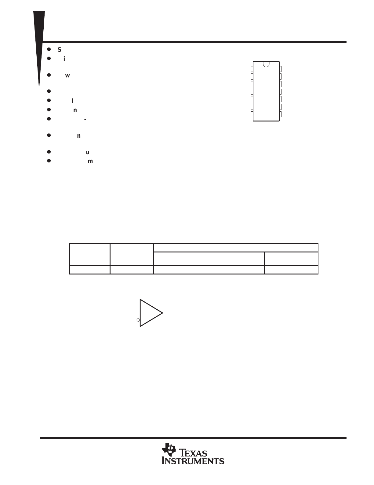
D, J, OR N PACKAGE
(TOP VIEW)
1OUT
2OUT
V
CC
2IN–
2IN+
1IN–
1IN+
1
2
3
4
5
6
7
14
13
12
11
10
9
8
3OUT
4OUT
GND
4IN+
4IN–
3IN+
3IN–
Includes Ground
D
Differential Input Voltage Range Equal to
Maximum-Rated Supply Voltage . . . ±28 V
D
Low Output Saturation Voltage
D
Output Compatible With TTL, MOS, and
CMOS
description
This device consists of four independent voltage comparators that are designed to operate from a single power
supply over a wide range of voltages. Operation from dual supplies is also possible so long as the difference
between the two supplies is 2 V to 28 V and V
voltage. Current drain is independent of the supply voltage. The outputs can be connected to other
open-collector outputs to achieve wired-AND relationships.
is a least 1.5 V more positive than the input common-mode
CC
T
A
–40°C to 85°C 20 mV LM3302D LM3302J LM3302N
†
The D packages are available taped and reeled. Add the suffix R to the device type, when ordering (i.e., LM3302DR).
VIOmax at 25°C
symbol (each comparator)
IN +
IN –
AVAILABLE OPTIONS
SMALL OUTLINE
(D)
†
OUT
PACKAGE
CERAMIC DIP
(J)
PLASTIC DIP
(N)
PRODUCTION DATA information is current as of publication date.
Products conform to specifications per the terms of Texas Instruments
standard warranty. Production processing does not necessarily include
testing of all parameters.
POST OFFICE BOX 655303 • DALLAS, TEXAS 75265
Copyright 1988, Texas Instruments Incorporated
1
Page 2
LM3302
QUADRUPLE DIFFERENTIAL COMPARATOR
SLCS014 –OCTOBER 1977 –REVISED APRIL 1988
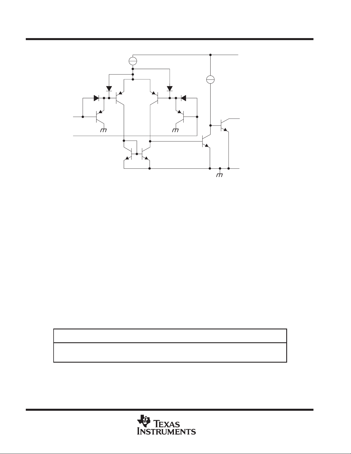
schematic
80-µA Current
Regulator
V
CC
10 µA
IN +
IN –
Current values shown are nominal.
60 µA
10 µA
80 µA
OUT
GND
absolute maximum ratings over operating free-air temperature range (unless otherwise noted)
Supply voltage, V
Differential input voltage, V
Input voltage range, V
Output voltage, V
Output current, I
Duration of output short-circuit to ground (see Note 3) unlimited. . . . . . . . . . . . . . . . . . . . . . . . . . . . . . . . . . . . .
Continuous total dissipation See Dissipation Rating Table. . . . . . . . . . . . . . . . . . . . . . . . . . . . . . . . . . . . . . . . . . .
Operating free-air temperature range, T
Storage temperature range – 65°C to 150°C. . . . . . . . . . . . . . . . . . . . . . . . . . . . . . . . . . . . . . . . . . . . . . . . . . . . . . .
Lead temperature range 1,6 mm (1/16 inch) from case for 60 seconds: J package 300°C. . . . . . . . . . . . . . . .
Lead temperature range 1,6 mm (1/16 inch) from case for 10 seconds: D or N package 260°C. . . . . . . . . . .
†
Stresses beyond those listed under absolute maximum ratings may cause permanent damage to the device. There are stress ratings only, and
functional operation of the device at these or any other conditions beyond those indicated in the recommended operating conditions section of this
specification is not implied. Exposure to absolute-maximum-rated conditions for extended periods may affect device reliability.
NOTES: 1. All voltage values, except differential voltages, are with respect to the network ground.
2. Differential voltages are at IN+ with respect to IN –.
3. Short circuits from the output to VCC can cause excessive heating and eventual destruction.
(see Note 1) 28 V. . . . . . . . . . . . . . . . . . . . . . . . . . . . . . . . . . . . . . . . . . . . . . . . . . . . . . . . . . .
CC
I
28 V. . . . . . . . . . . . . . . . . . . . . . . . . . . . . . . . . . . . . . . . . . . . . . . . . . . . . . . . . . . . . . . . . . . . . . . .
O
20 mA. . . . . . . . . . . . . . . . . . . . . . . . . . . . . . . . . . . . . . . . . . . . . . . . . . . . . . . . . . . . . . . . . . . . . . . .
O
(see Note 2) ±28 V. . . . . . . . . . . . . . . . . . . . . . . . . . . . . . . . . . . . . . . . . . . . . . . . . .
ID
(either input), VI – 0.3 V to 28 V. . . . . . . . . . . . . . . . . . . . . . . . . . . . . . . . . . . . . . . . . . . . .
– 40°C to 85°C. . . . . . . . . . . . . . . . . . . . . . . . . . . . . . . . . . . . . . . . . . .
A
†
DISSIPATION RATING TABLE
PACKAGE
D
J
N
2
TA ≤ 25°C
POWER RATING
950 mW
1025 mW
1150 mW
DERATING FACTOR
ABOVE TA = 25°C
7.6 mW/°C
8.2 mW/°C
9.2 mW/°C
POST OFFICE BOX 655303 • DALLAS, TEXAS 75265
TA = 70°C
POWER RATING
608 mW
656 mW
736 mW
TA = 85°C
POWER RATING
494 mW
533 mW
598 mW
Page 3

VIOInput offset voltage
CC
,
IC ICR
,
mV
IIOInput offset voltage
V
V
nA
IIBInput bias current
nA
V
V
Large-signal differential
V
CC
V
O
A
VD
lificati
RL
V
25 C
2
30
V/mV
IOHHigh-level output current
V
1 V
V
5 V
VOLLow-level output voltage
V
V
V
mV
Response time
L
,
L
,
s
LM3302
QUADRUPLE DIFFERENTIAL COMPARATOR
SLCS014 –OCTOBER 1977 –REVISED APRIL 1988
electrical characteristics at specified free-air temperature, VCC = 5 V (unless otherwise noted)
PARAMETER
p
p
p
Common-mode input
ICR
voltage range
A
voltage amp
I
Low-level output current VID = 1 V, VOL = 1.5 V 25°C 6 16 mA
OL
Supply current
I
CC
(four comparators)
‡
All characteristics are measured with zero common-mode input voltage unless otherwise specified.
on
p
p
p
V
VO = 1.4 V
O
ID
ID
VO = 2.5 V, No load 25°C 0.8 mA
TEST CONDITIONS
= 5 V to 28 V, V
= 1.4
= 15 V,
= 15 Ω to
=
= 1 V,
CC
,
‡
= V
min,
= 1.4 V to 11.4 V,
=
OH
= 5
OH
T
A
25°C 3 20
–40°C to 85°C 40
25°C 3 100
–40°C to 85°C 300
25°C – 25 – 500
–40°C to 85°C –1000
25°C
–40°C to 85°C
25°C
25°C 0.1 nA
–40°C to 85°C 1 µA
25°C 150 500
–40°C to 85°C 700
MIN TYP MAX UNIT
0 to
VCC – 1.5
0 to
VCC – 2
2 30 V/mV
switching characteristics, VCC = 5 V, TA = 25°C
PARAMETER TEST CONDITIONS MIN TYP MAX UNIT
R
p
†
CL includes probe and jig capacitance.
NOTE 4: The response time specified is the interval between the input step function and the instant when the output crosses 1.4 V.
= 5.1 kΩ to 5 V,
See Note 4
C
= 15 pF†,
100-mV input step with 5-mV overdrive 1.3
TTL-level input step 0.3
µ
POST OFFICE BOX 655303 • DALLAS, TEXAS 75265
3
Page 4

IMPORTANT NOTICE
T exas Instruments and its subsidiaries (TI) reserve the right to make changes to their products or to discontinue
any product or service without notice, and advise customers to obtain the latest version of relevant information
to verify, before placing orders, that information being relied on is current and complete. All products are sold
subject to the terms and conditions of sale supplied at the time of order acknowledgement, including those
pertaining to warranty, patent infringement, and limitation of liability.
TI warrants performance of its semiconductor products to the specifications applicable at the time of sale in
accordance with TI’s standard warranty. Testing and other quality control techniques are utilized to the extent
TI deems necessary to support this warranty . Specific testing of all parameters of each device is not necessarily
performed, except those mandated by government requirements.
CERT AIN APPLICATIONS USING SEMICONDUCTOR PRODUCTS MAY INVOLVE POTENTIAL RISKS OF
DEATH, PERSONAL INJURY, OR SEVERE PROPERTY OR ENVIRONMENTAL DAMAGE (“CRITICAL
APPLICATIONS”). TI SEMICONDUCTOR PRODUCTS ARE NOT DESIGNED, AUTHORIZED, OR
WARRANTED TO BE SUITABLE FOR USE IN LIFE-SUPPORT DEVICES OR SYSTEMS OR OTHER
CRITICAL APPLICA TIONS. INCLUSION OF TI PRODUCTS IN SUCH APPLICATIONS IS UNDERST OOD TO
BE FULLY AT THE CUSTOMER’S RISK.
In order to minimize risks associated with the customer’s applications, adequate design and operating
safeguards must be provided by the customer to minimize inherent or procedural hazards.
TI assumes no liability for applications assistance or customer product design. TI does not warrant or represent
that any license, either express or implied, is granted under any patent right, copyright, mask work right, or other
intellectual property right of TI covering or relating to any combination, machine, or process in which such
semiconductor products or services might be or are used. TI’s publication of information regarding any third
party’s products or services does not constitute TI’s approval, warranty or endorsement thereof.
Copyright 1998, Texas Instruments Incorporated
 Loading...