

LM317M
3-TERMINAL ADJUSTABLE REGULATOR
SLVS297 – APRIL 2000
D
Output V oltage Range Adjustable From
1.2 V to 37 V
D
Output Current Greater Than 500 mA
D
Internal Short-Circuit Current Limiting
D
Thermal Overload Protection
D
Output Safe-Area Compensation
description
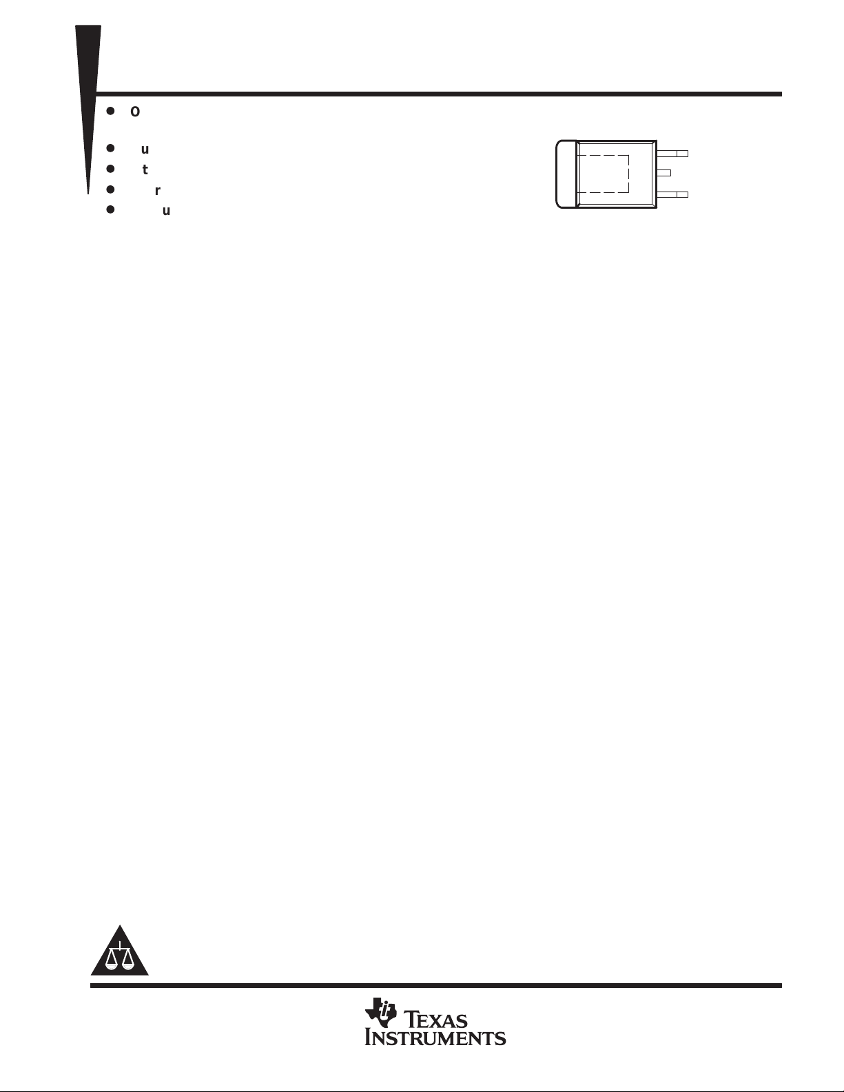
OUTPUT
The OUTPUT terminal is in electrical contact with
the mounting base.
KTP PACKAGE
(TOP VIEW)
INPUT
ADJUST
The LM317M device is an adjustable 3-terminal positive voltage regulator capable of supplying more than
500 mA over an output-voltage range of 1.2 V to 37 V. It is exceptionally easy to use and requires only two
external resistors to set the output voltage. Further, both line and load regulation are better than standard fixed
regulators. The LM317M is packaged in the DP AK/TO-252-equivalent KTP package, which is easy to handle
and use.
In addition to higher performance than fixed regulators, the device includes on-chip current limiting, thermal
overload protection, and safe operating area protection. All overload protection remains fully functional if the
ADJUST terminal is disconnected.
Normally , no capacitors are needed unless the device is more than 6 inches from the input filter capacitors, in
which case an input bypass capacitor is needed. An optional output capacitor can be added to improve transient
response. The ADJUST terminal can be bypassed to achieve very high ripple-rejection ratios, which are difficult
to achieve with standard 3-terminal regulators.
The LM317M is characterized for operation over the virtual junction temperature range of 0°C to 125°C.
Please be aware that an important notice concerning availability, standard warranty, and use in critical applications of
Texas Instruments semiconductor products and disclaimers thereto appears at the end of this data sheet.
PRODUCTION DATA information is current as of publication date.
Products conform to specifications per the terms of Texas Instruments
standard warranty. Production processing does not necessarily include
testing of all parameters.
POST OFFICE BOX 655303 • DALLAS, TEXAS 75265
Copyright 2000, Texas Instruments Incorporated
1
LM317M
Line regulation (see Note 3)
V
V
V
%/V
Load regulation
I
500 mA
%V
Ripple rejection (see Note 4)
O
,,
dB
3-TERMINAL ADJUSTABLE REGULATOR
SLVS297 – APRIL 2000
absolute maximum ratings over operating temperature range (unless otherwise noted)
Input-to-output differential voltage, V
– VO 40 V. . . . . . . . . . . . . . . . . . . . . . . . . . . . . . . . . . . . . . . . . . . . . . . . . . . .
l
†
Package thermal impedance, θJA (see Notes 1 and 2) 28°C/W. . . . . . . . . . . . . . . . . . . . . . . . . . . . . . . . . . . . . . .
Lead temperature 1,6 mm (1/16 inch) from case for 10 seconds 260°C. . . . . . . . . . . . . . . . . . . . . . . . . . . . . . .
Storage temperature range, T
†
Stresses beyond those listed under “absolute maximum ratings” may cause permanent damage to the device. These are stress ratings only, and
functional operation of the device at these or any other conditions beyond those indicated under “recommended operating conditions” is not
implied. Exposure to absolute-maximum-rated conditions for extended periods may affect device reliability.
NOTES: 1. Maximum power dissipation is a function of TJ(max), θJA, and TA. The maximum allowable power dissipation at any allowable
ambient temperature is PD = (TJ(max) – TA)/θJA. Operating at the absolute maximum TJ of 150°C can impact reliability.
2. The package thermal impedance is calculated in accordance with JESD 51.
–65°C to 150°C. . . . . . . . . . . . . . . . . . . . . . . . . . . . . . . . . . . . . . . . . . . . . . . . . . .
stg
recommended operating conditions
MIN MAX UNIT
Input-to-output voltage differential, VI – V
Output current, I
Operating virtual-junction temperature, T
O
O
J
37 V
500 mA
0 125 °C
electrical characteristics over recommended operating virtual-junction temperature range,
V
– VO = 5 V, IO = 0.1 A (unless otherwise noted)
I
PARAMETER TEST CONDITIONS
–
= 3 V to 40
I
O
= 10 mA to
O
ADJUST terminal current 50 100 µA
ADJUST terminal current change VI – VO = 3 V to 40 V, IO = 10 mA to 500 mA 0.2 5 µA
Reference voltage VI – VO = 3 V to 40 V, IO = 10 mA to 500 mA 1.2 1.25 1.3 V
Output-voltage temperature stability 0.7%
Minimum load current to maintain regulation 3.5 10 mA
VI – VO ≤ 15 V 500 900
Maximum output current
Output noise voltage (% of VO) f = 10 Hz to 10 KHz, TJ = 25°C 0.003%
pp
Long-term stability TJ = 125°C 0.3 1
‡
Pulse-testing techniques are used to maintain the junction temperature as close to the ambient temperature as possible.
NOTES: 3. Input voltage regulation is expressed here as the percentage change in output voltage per 1-V change at the input.
4. C
is connected between the ADJUST pin and ground.
ADJ
VI – VO = 40 V,
Pd ≤ P
d(max)
V
= 10 V, f = 120 Hz,
TJ = 25°C
TJ = 25°C 0.01 0.04
Full temperature range 0.02 0.07
TJ = 25°C 0.1 0.5
Full temperature range 0.3 1.5
TJ = 25°C 150 250
C
C
‡
= 0 65
ADJ
= 10 µF 66 80
ADJ
MIN TYP MAX UNIT
O
mA
%/
1k Hrs
2
POST OFFICE BOX 655303 • DALLAS, TEXAS 75265
LM317M
3-TERMINAL ADJUSTABLE REGULATOR
SLVS297 – APRIL 2000
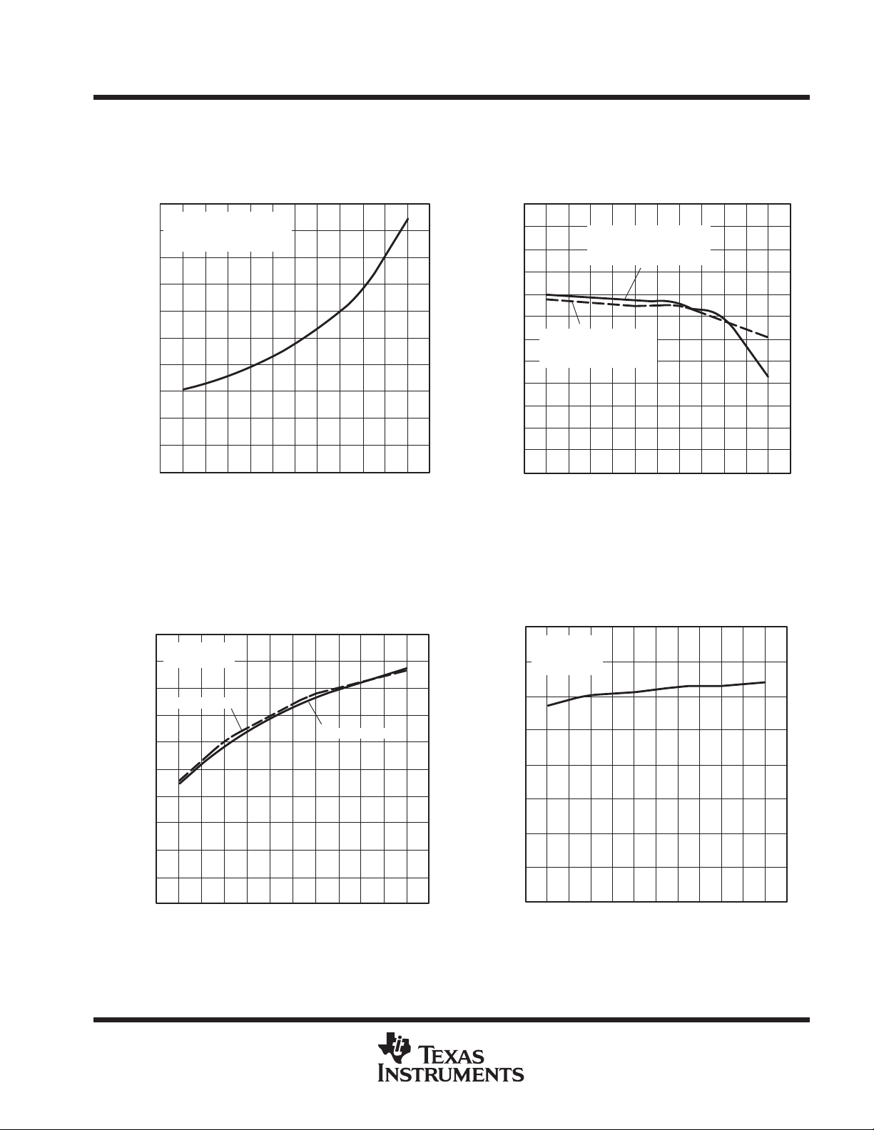
TYPICAL CHARACTERISTICS
1.00
VI = 4.25 V to 41.25 V
VO = V
0.90
IL = 10 mA
0.80
0.70
0.60
0.50
0.40
0.30
– Output V oltage Change – %
O
0.20
∆V
0.10
0
0 25 50 75 100 125
LINE REGULATION
TEMPERATURE
ref
TJ – Temperature – °C
Figure 1
vs
0.20
0.15
0.10
0.05
0.00
–0.05
–0.10
–0.15
–0.20
– Output V oltage Change – %
O
–0.25
∆V
–0.30
–0.35
–0.40
VI = 10 V
VO = 5 V
IL = 10 mA to 40 mA
02550
LOAD REGULATION
vs
TEMPERATURE
VI = 45 V
VO = 5 V
IL = 10 mA to 100 mA
75 100 125
TJ – Temperature – °C
Figure 2
ADJUST TERMINAL CURRENT
55
VI = 6.25 V
VO = V
53
A
51
µ
ADJUST Terminal Current –
IL = 100 mA
49
47
45
43
41
39
37
35
02550
vs
TEMPERATURE
ref
TJ – Temperature – °C
Figure 3
IL = 10 mA
75 100 125
1.260
1.255
1.250
1.245
1.240
1.235
– Reference Voltage – V
ref
1.230
V
1.225
1.220
TEMPERATURE STABILITY
vs
TEMPERATURE
VI = 4.25 V
VO = V
ref
IL = 10 mA
02550
TJ – Temperature – °C
Figure 4
75 100 125
POST OFFICE BOX 655303 • DALLAS, TEXAS 75265
3

LM317M
3-TERMINAL ADJUSTABLE REGULATOR
SLVS297 – APRIL 2000
TYPICAL CHARACTERISTICS
MINIMUM OPERATING CURRENT
vs
INPUT-OUTPUT DIFFERENTIAL VOLTAGE
8
7
6
5
4
3
2
Minimum Operating Current – mA
1
0
0 5 10 15 20
VI-VO – Input-Output Differential – V
Figure 5
TJ = 125°C
TJ = 25°C
25 30 35 40
INPUT-OUTPUT DIFFERENTIAL VOLTAGE
1.00
0.80
0.60
– Output Current – A
0.40
O
I
0.20
0.00
0 5 10 15
OUTPUT CURRENT LIMIT
vs
TJ = 25°C
TJ = 125°C
20 25 30 35 40
VI-VO – Input-Output Differential – V
Figure 6
O
% V
Ouput Noise Voltage –
0.004
0.003
0.002
0.001
0.000
OUTPUT NOISE VOLTAGE
vs
TEMPERATURE
VI = 15 V
VO = 10 V
IL = 50 mA
Bandwidth = 10 Hz to 10 KHz
02550
TJ – Temperature – °C
75 100 125
Figure 7
RIPPLE REJECTION
vs
TEMPERATURE
90
VI = 15 Vdc and 1 VPP (120 Hz)
VO = 10 V
85
IL = 100 mA
CL = 1 µF
80
Ci = 0.1 µF
75
70
65
Ripple Rejection – dB
60
55
50
45
02570
C
= 0 µF
ADJ
TJ – Temperature – °C
Figure 8
C
= 10 µF
ADJ
85 125
4
POST OFFICE BOX 655303 • DALLAS, TEXAS 75265

LM317M
3-TERMINAL ADJUSTABLE REGULATOR
SLVS297 – APRIL 2000
TYPICAL CHARACTERISTICS
100
90
80
70
60
50
40
Ripple Rejection – dB
30
VI = 15 Vdc and Vac = 1 V
20
VO = 10 V
IL = 100 mA
10
CL = 1 µF
Ci = 0.1 µF
0
10 Hz
100 Hz
RIPPLE REJECTION
vs
FREQUENCY
C
= 10 µF
ADJ
C
= 0 µF
ADJ
PP
1 kHz
Frequency
Figure 9
10 kHz 100 kHz
) – Input-Output Voltage Differential – V
O
– V
I
(V
INPUT-OUTPUT VOLTAGE DIFFERENTIAL
vs
TEMPERATURE
2.5
2
1.5
IL = 100 mA
1
0.5
0
02550
TJ – Temperature – °C
75 100 125
Figure 10
IL = 500 mA
10.00
Ω
Output Impedance –
VI = 15 V
VO = 10 V
IL = 100 mA dc and 10 mA RMS
1.00
0.10
0.01
10 Hz
OUTPUT IMPEDANCE
50 Hz 100 Hz 500 Hz
vs
FREQUENCY
C
= 0 µF
ADJ
C
= 10 µF
ADJ
1 kHz 5 kHz 10 kHz 50 kHz 100 kHz
Frequency
Figure 11
150 kHz
POST OFFICE BOX 655303 • DALLAS, TEXAS 75265
5

LM317M
3-TERMINAL ADJUSTABLE REGULATOR
SLVS297 – APRIL 2000
TYPICAL CHARACTERISTICS
LINE TRANSIENT RESPONSE
1
0.8
0.6
0.4
0.2
0
VO = 10 V
–0.2
VI = 15 V, ∆VI = +1 V
–0.4
–0.6
–0.8
–1
1.2
0.8
0.6
0.4
0.2
IL = 50 mA
TJ = 25°C
CL = 0 µF
C
= 0 µF
ADJ
1
0
–1.0
–0.5 0 0.5 1.0 1.5 2.0 2.5 3.0 3.5 4.0 4.5
– Output Voltage Change – V
O
∆V
– Input V oltage change – V
I
∆V
vs
TIME
Time – µs
Figure 12
6
POST OFFICE BOX 655303 • DALLAS, TEXAS 75265

LM317M
3-TERMINAL ADJUSTABLE REGULATOR
SLVS297 – APRIL 2000
TYPICAL CHARACTERISTICS
LOAD TRANSIENT RESPONSE
vs
TIME
5.0
VI = 15 V
4.0
VO = 10 V
IL = 50 mA
3.0
∆IL = +500 mA
2.0
1.0
0
–1.0
– Output Voltage Change – V
O
–2.0
∆V
–3.0
–4.0
0.6
0.5
0.4
0.3
0.2
0.1
0
–0.1
–0.2
– Output Current Change – A
–10
O
∆I
–5 0 5 10 15 20 25 30 35
CL = 1 µF
C
= 10 µF
ADJ
CL = 0 µF
C
ADJ
= 0 µF
Time – µs
Figure 13
POST OFFICE BOX 655303 • DALLAS, TEXAS 75265
7

IMPORTANT NOTICE
T exas Instruments and its subsidiaries (TI) reserve the right to make changes to their products or to discontinue
any product or service without notice, and advise customers to obtain the latest version of relevant information
to verify, before placing orders, that information being relied on is current and complete. All products are sold
subject to the terms and conditions of sale supplied at the time of order acknowledgment, including those
pertaining to warranty, patent infringement, and limitation of liability.
TI warrants performance of its semiconductor products to the specifications applicable at the time of sale in
accordance with TI’s standard warranty. Testing and other quality control techniques are utilized to the extent
TI deems necessary to support this warranty . Specific testing of all parameters of each device is not necessarily
performed, except those mandated by government requirements.
Customers are responsible for their applications using TI components.
In order to minimize risks associated with the customer’s applications, adequate design and operating
safeguards must be provided by the customer to minimize inherent or procedural hazards.
TI assumes no liability for applications assistance or customer product design. TI does not warrant or represent
that any license, either express or implied, is granted under any patent right, copyright, mask work right, or other
intellectual property right of TI covering or relating to any combination, machine, or process in which such
semiconductor products or services might be or are used. TI’s publication of information regarding any third
party’s products or services does not constitute TI’s approval, warranty or endorsement thereof.
Copyright 2000, Texas Instruments Incorporated
 Loading...