


LM237, LM337
CHIP
3-TERMINAL ADJUSTABLE REGULATORS
SLVS047C – NOVEMBER 1981 – REVISED JULY 1999
D
Output V oltage Range Adjustable From
–1.2 V to –37 V
D
Output Current Capability of 1.5 A Max
D
Input Regulation Typically 0.01% Per
Input-Voltage Change
D
Output Regulation Typically 0.3%
D
Peak Output Current Constant Over
Temperature Range of Regulator
D
Ripple Rejection Typically 77 dB
D
Direct Replacement for National
Semiconductor LM237 and LM337
description
The LM237 and LM337 are adjustable 3-terminal
negative-voltage regulators capable of supplying
in excess of –1.5 A over an output voltage range
of –1.2 V to –37 V . They are exceptionally easy to
use, requiring only two external resistors to set the
output voltage and one output capacitor for
frequency compensation. The current design has
been optimized for excellent regulation and low
thermal transients. In addition, the LM237 and
LM337 feature internal current limiting, thermal
shutdown, and safe-area compensation, making
them virtually immune to failure by overloads.
The LM237 and LM337 serve a wide variety of
applications, including local on-card regulation,
programmable output-voltage regulation, and
precision current regulation.
KC PACKAGE
(TOP VIEW)
OUTPUT
INPUT
ADJUSTMENT
The INPUT terminal is in electrical
contact with the mounting base.
TO-220AB
O
I
A
KTE PACKAGE
(TOP VIEW)
OUTPUT
INPUT
ADJUSTMENT
The INPUT terminal is in electrical contact with the mounting base.
O
I
A
The LM237 is characterized for operation over the
virtual junction temperature range of –25°C to
150°C. The LM337 is characterized for operation
over the virtual junction temperature range of 0°C
to 125°C.
T
J
–25°C to 150°C LM237KC LM237KTE —
0°C to 125°C LM337KC LM337KTE LM337Y
The KTE package is only available taped and reeled. Add the R suffix to the device type (e.g.,
LM237KTER). Chip forms are tested at 25°C.
Please be aware that an important notice concerning availability, standard warranty, and use in critical applications of
Texas Instruments semiconductor products and disclaimers thereto appears at the end of this data sheet.
PRODUCTION DATA information is current as of publication date.
Products conform to specifications per the terms of Texas Instruments
standard warranty. Production processing does not necessarily include
testing of all parameters.
HEAT-SINK MOUNTED
POST OFFICE BOX 655303 • DALLAS, TEXAS 75265
AVAILABLE OPTIONS
PACKAGED DEVICES
(KC)
PLASTIC
FLANGE MOUNTED
(KTE)
FORM
(Y)
Copyright 1999, Texas Instruments Incorporated
1
LM237, LM337
Output current, I
mA
O erating virtual junction tem erature, T
J
°C
3-TERMINAL ADJUSTABLE REGULATORS
SLVS047C – NOVEMBER 1981 – REVISED JULY 1999
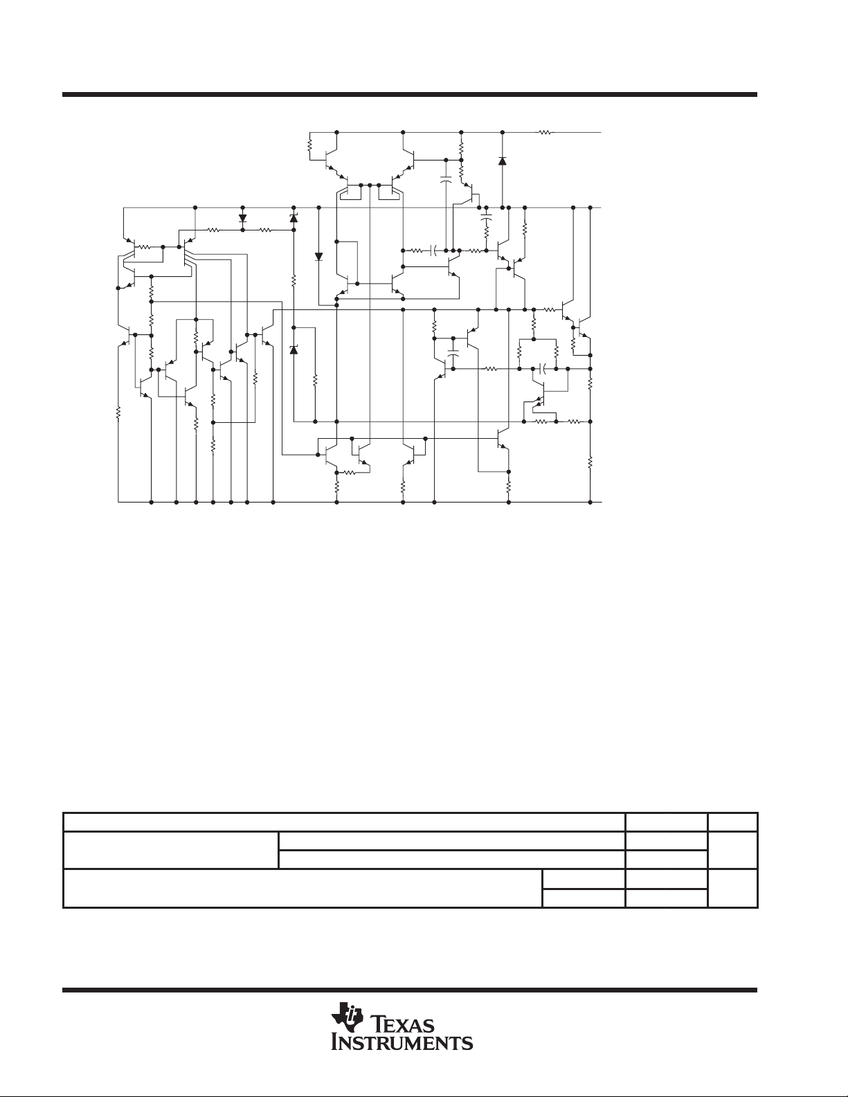
schematic diagram
ADJUSTMENT
OUTPUT
INPUT
absolute maximum ratings over operating temperature ranges (unless otherwise noted)
†
Input-to-output differential voltage, VI – VO –40 V. . . . . . . . . . . . . . . . . . . . . . . . . . . . . . . . . . . . . . . . . . . . . . . . . . .
Package thermal impedance, θ
(see Notes 1 and 2): KC package 22°C/W. . . . . . . . . . . . . . . . . . . . . . . . . . .
JA
KTE package 23°C/W. . . . . . . . . . . . . . . . . . . . . . . . . .
Lead temperature 1,6 mm (1/16 inch) from case for 10 seconds 260°C. . . . . . . . . . . . . . . . . . . . . . . . . . . . . . .
Storage temperature range, T
†
Stresses beyond those listed under “absolute maximum ratings” may cause permanent damage to the device. These are stress ratings only, and
functional operation of the device at these or any other conditions beyond those indicated under “recommended operating conditions” is not
implied. Exposure to absolute-maximum-rated conditions for extended periods may affect device reliability.
NOTES: 1. Maximum power dissipation is a function of TJ(max),
ambient temperature is PD = (TJ(max) – TA)/
variations in individual device electrical characteristics and thermal resistance, the built-in thermal overload protection may be
activated at power levels slightly above or below the rated dissipation.
2. The package thermal impedance is calculated in accordance with JESD 51, except for through-hole packages, which use a trace
length of zero.
–65°C to 150°C. . . . . . . . . . . . . . . . . . . . . . . . . . . . . . . . . . . . . . . . . . . . . . . . . . .
stg
θ
, and TA. The maximum allowable power dissipation at any allowable
θ
JA
JA
. Operating at the absolute maximum TJ of 150°C can impact reliability. Due to
recommended operating conditions
MIN MAX UNIT
p
p
O
p
|VI – VO| ≤ 40 V, P ≤ 15 W 10 1500
|VI – VO| ≤ 10 V, P ≤ 15 W 6 1500
LM237 –25 150
LM337 0 125
°
2
POST OFFICE BOX 655303 • DALLAS, TEXAS 75265

LM237, LM337
PARAMETER
TEST CONDITIONS
†
UNIT
I
‡
V
V
3 V to –40 V
%/V
Ripple rejection
dB
O
,
Output regulation
I
10 mA to 1.5 A
mA
Peak output current
A
g
I
V
3-TERMINAL ADJUSTABLE REGULATORS
SLVS047C – NOVEMBER 1981 – REVISED JULY 1999
electrical characteristics over recommended ranges of operating virtual junction temperature
(unless otherwise noted)
LM237 LM337
MIN TYP MAX MIN TYP MAX
–
nput regulation
pp
p
Output-voltage
change with
temperature
Output-voltage
long-term drift
Output noise
voltage
Minimum output
current to maintain
regulation
p
Adjustment-terminal
current
Change in
adjustment-terminal
current
Reference voltage
(output to ADJ)
Thermal regulation Initial TJ = 25°C, 10-ms pulse 0.002 0.02 0.003 0.04 %/W
†
Unless otherwise noted, these specifications apply for the following test conditions |VI – VO| = 5 V and IO = 0.5 A. For conditions shown as MIN
or MAX, use the appropriate value specified under recommended operating conditions. All characteristics are measured with a 0.1-µF capacitor
across the input and a 1-µF capacitor across the output. Pulse-testing techniques are used to maintain the junction temperature as close to the
ambient temperature as possible. Thermal effects must be taken into account separately.
‡
Input regulation is expressed here as the percentage change in output voltage per 1-V change at the input.
= –
I
O
VO = –10 V, f = 120 HZ 60 60
VO = –10 V, f = 120 HZ, C
I
= 10 mA to 1.5 A,
TJ = 25°C
=
O
TJ = MIN to MAX 0.6% 0.6%
After 1000 h at TJ = MAX and VI – VO = –40 V 0.3% 1% 0.3% 1%
f = 10 HZ to 10 kHZ, TJ = 25°C 0.003% 0.003%
|VI – VO| ≤ 40 V 2.5 5 2.5 10
|VI – VO| ≤ 10 V 1.2 3 1.5 6
|VI – VO| ≤ 15 V 1.5 2.2 1.5 2.2
|VI – VO| ≤ 40 V, TJ = 25°C 0.24 0.4 0.15 0.4
VI – VO = – 2.5 V to –40 V,
IO = 10 mA to MAX
VI – VO = – 3 V to –40 V,
= 10 mA to 1.5 A,
O
P ≤ rated dissipation
TJ = 25°C 0.01 0.02 0.01 0.04
TJ = MIN to MAX 0.02 0.05 0.02 0.07
= 10 µF 66 77 66 77
ADJ
|VO| ≤ 5 V 25 50 mV
|VO| ≥ 5 V 0.3% 0.5% 0.3% 1%
|VO| ≤ 5 V 50 70 mV
|VO| ≥ 5 V 1% 1.5%
65 100 65 100 µA
TJ = 25°C,
TJ = 25°C –1.225 –1.25 –1.275 –1.213 –1.25 –1.287
TJ = MIN to MAX –1.2 –1.25 –1.3 –1.2 –1.25 –1.3
2 5 2 5 µA
POST OFFICE BOX 655303 • DALLAS, TEXAS 75265
3

LM237, LM337
PARAMETER
TEST CONDITIONS
†
UNIT
Ripple rejection
dB
Output regulation
I
10 mA to 1.5 A
Minimum output current to maintain regulation
mA
Peak output current
A
3-TERMINAL ADJUSTABLE REGULATORS
SLVS047C – NOVEMBER 1981 – REVISED JULY 1999
electrical characteristics, TJ = 25°C
LM237, LM337
MIN TYP MAX
Input regulation
pp
p
Output noise voltage f = 10 HZ to 10 kHZ 0.003%
Adjustment-terminal current 65 100 µA
Change in adjustment-terminal current VI – VO = – 2.5 V to –40 V, IO = 10 mA to MAX 2 5 µA
Reference voltage (output to ADJ)
†
Unless otherwise noted, these specifications apply for the following test conditions |VI – VO| = 5 V and IO = 0.5 A. All characteristics are measured
with a 0.1-µF capacitor across the input and a 1-µF capacitor across the output. Pulse-testing techniques are used to maintain the junction
temperature as close to the ambient temperature as possible. Thermal effects must be taken into account separately.
‡
Input regulation is expressed here as the percentage change in output voltage per 1-V change at the input.
‡
p
p
VI – VO = –3 V to –40 V 0.01 0.04 %/V
VO = –10 V, f = 120 HZ 60
VO = –10 V, C
=
O
|VI – VO| ≤ 40 V 2.5 10
|VI – VO| ≤ 10 V 1.5 6
|VI – VO| ≤ 15 V 1.5 2.2
|VI – VO| ≤ 40 V 0.15 0.4
VI – VO = – 3 V to –40 V, IO = 10 mA to 1.5 A,
P ≤ rated dissipation
= 10 µF, f = 120 HZ 66 77
ADJ
|VO| ≤ 5 V 50 mV
|VO| ≥ 5 V 0.3% 1%
–1.213 –1.25 –1.287 V
4
POST OFFICE BOX 655303 • DALLAS, TEXAS 75265
3-TERMINAL ADJUSTABLE REGULATORS
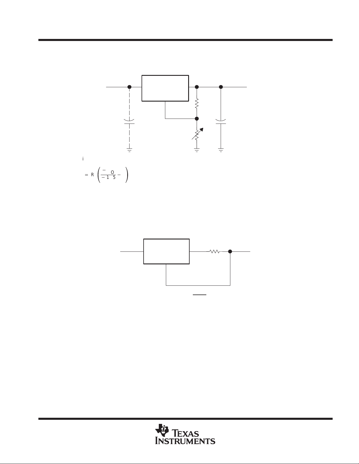
APPLICATION INFORMATION
LM237
or
LM337
LM237, LM337
SLVS047C – NOVEMBER 1981 – REVISED JULY 1999
V
I
C1
R1 is typically 120 Ω.
*
V
O
R2+R1
C1 is a 1-µF solid tantalum capacitor required only if the regulator is more than 10 cm (4 in) from the power-supply filter capacitor.
C2 is a 1-µF solid tantalum or 10-µF aluminum electrolytic capacitor required for stability.
ǒ
*
1.25
*
1
Ǔ
INPUT
+
where VO is the output in volts.
OUTPUT
ADJUSTMENT
R1
R2
V
O
C2
+
Figure 1. Adjustable Negative-Voltage Regulator
LM237
or
LM337
R
V
I
OUTPUTINPUT
ADJUSTMENT
S
V
O
1.25 V
I
LIMIT
RS =
Figure 2. Current-Limiting Circuit
POST OFFICE BOX 655303 • DALLAS, TEXAS 75265
5

IMPORTANT NOTICE
T exas Instruments and its subsidiaries (TI) reserve the right to make changes to their products or to discontinue
any product or service without notice, and advise customers to obtain the latest version of relevant information
to verify, before placing orders, that information being relied on is current and complete. All products are sold
subject to the terms and conditions of sale supplied at the time of order acknowledgement, including those
pertaining to warranty, patent infringement, and limitation of liability.
TI warrants performance of its semiconductor products to the specifications applicable at the time of sale in
accordance with TI’s standard warranty. Testing and other quality control techniques are utilized to the extent
TI deems necessary to support this warranty . Specific testing of all parameters of each device is not necessarily
performed, except those mandated by government requirements.
CERTAIN APPLICA TIONS USING SEMICONDUCT OR PRODUCTS MAY INVOLVE POTENTIAL RISKS OF
DEATH, PERSONAL INJURY, OR SEVERE PROPERTY OR ENVIRONMENTAL DAMAGE (“CRITICAL
APPLICATIONS”). TI SEMICONDUCTOR PRODUCTS ARE NOT DESIGNED, AUTHORIZED, OR
WARRANTED TO BE SUITABLE FOR USE IN LIFE-SUPPORT DEVICES OR SYSTEMS OR OTHER
CRITICAL APPLICA TIONS. INCLUSION OF TI PRODUCTS IN SUCH APPLICATIONS IS UNDERST OOD TO
BE FULLY AT THE CUSTOMER’S RISK.
In order to minimize risks associated with the customer’s applications, adequate design and operating
safeguards must be provided by the customer to minimize inherent or procedural hazards.
TI assumes no liability for applications assistance or customer product design. TI does not warrant or represent
that any license, either express or implied, is granted under any patent right, copyright, mask work right, or other
intellectual property right of TI covering or relating to any combination, machine, or process in which such
semiconductor products or services might be or are used. TI’s publication of information regarding any third
party’s products or services does not constitute TI’s approval, warranty or endorsement thereof.
Copyright 1999, Texas Instruments Incorporated
 Loading...