

Page 1
INA270
INA271
FEATURES DESCRIPTION
APPLICATIONS
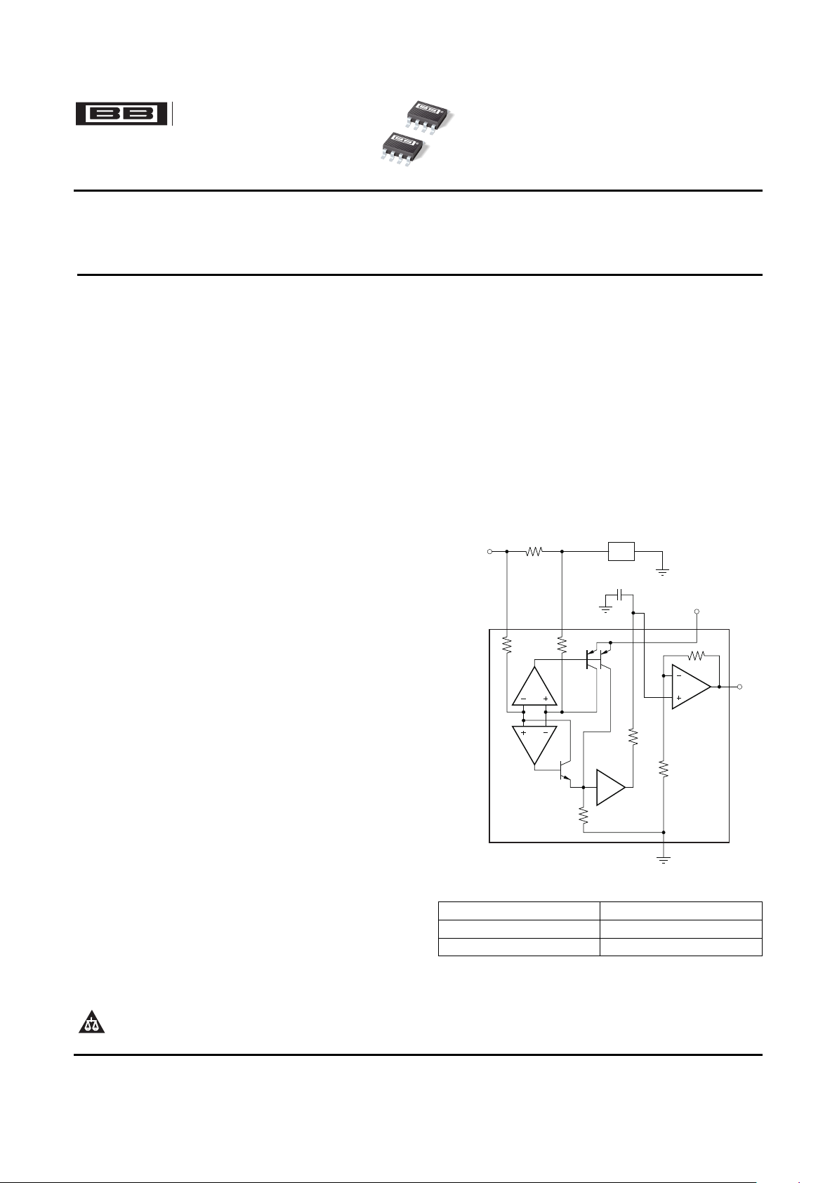
A1
A2
Single-PoleFilter
Capacitor
+2.7Vto+18V
5kW5kW
96kW
R
L
PREOUT BUFIN
GND
OUT
IN-IN+ V+
Load
-16Vto+80V
Supply
R
S
INA270
INA270
INA271
SBOS381A – FEBRUARY 2007 – REVISED APRIL 2007
Voltage Output, Unidirectional Measurement
Current-Shunt Monitor
• WIDE COMMON-MODE RANGE: –16V to +80V
The INA270 and INA271 family of current-shunt
monitors with voltage output can sense drops across
• CMRR: 120dB
current shunts at common-mode voltages from –16V
• ACCURACY:
to +80V, independent of the supply voltage. The
± 2.5mV offset (max)
INA270 and INA271 pinouts readily enable filtering.
± 1% gain error (max)
The INA270 and INA271 are available with two
20 µ V/ ° C offset drift (max)
output voltage scales: 14V/V and 20V/V. The 130kHz
55ppm/ ° C gain drift (max)
bandwidth simplifies use in current-control loops.
• BANDWIDTH: Up to 130kHz
The INA270 and INA271 operate from a single +2.7V
• TWO TRANSFER FUNCTIONS AVAILABLE:
to +18V supply, drawing a maximum of 900 µ A of
14V/V (INA270)
supply current. They are specified over the extended
20V/V (INA271)
operating temperature range of –40 ° C to +125 ° C and
• QUIESCENT CURRENT: 900 µ A (max)
are offered in an SO-8 package.
• POWER SUPPLY: +2.7V to +18V
• PROVISION FOR FILTERING
• POWER MANAGEMENT
• AUTOMOTIVE
• TELECOM EQUIPMENT
• NOTEBOOK COMPUTERS
• BATTERY CHARGERS
• CELL PHONES
• WELDING EQUIPMENT
DEVICE COMPARISON
DEVICE GAIN
INA270 14V/V
INA271 20V/V
Please be aware that an important notice concerning availability, standard warranty, and use in critical applications of Texas
Instruments semiconductor products and disclaimers thereto appears at the end of this data sheet.
All trademarks are the property of their respective owners.
PRODUCTION DATA information is current as of publication date.
Copyright © 2007, Texas Instruments Incorporated
Products conform to specifications per the terms of the Texas
Instruments standard warranty. Production processing does not
necessarily include testing of all parameters.
Page 2
www.ti.com
ABSOLUTE MAXIMUM RATINGS
(1)
PIN CONFIGURATION
1
2
3
4
8
7
6
5
IN+
NC
(1)
V+
OUT
IN-
GND
PREOUT
BUFIN
INA27x
INA270
INA271
SBOS381A – FEBRUARY 2007 – REVISED APRIL 2007
This integrated circuit can be damaged by ESD. Texas Instruments recommends that all integrated circuits be handled with
appropriate precautions. Failure to observe proper handling and installation procedures can cause damage.
ESD damage can range from subtle performance degradation to complete device failure. Precision integrated circuits may be
more susceptible to damage because very small parametric changes could cause the device not to meet its published
specifications.
ORDERING INFORMATION
(1)
PACKAGE PACKAGE
PRODUCT PACKAGE-LEAD DESIGNATOR GAIN MARKING
INA270 SO-8 D 14 I270A
INA271 SO-8 D 20 I271A
(1) For the most current package and ordering information see the Package Option Addendum at the end of this document, or see the TI
web site at www.ti.com .
INA270, INA271 UNIT
Supply Voltage (VS) +18 V
Analog Inputs, V
IN+
, V
IN–
:
Differential, (V
IN+
) – (V
IN–
) –18 to +18 V
Common-Mode –16 to +80 V
Analog Output:
OUT and PRE OUT Pins GND – 0.3 to (V+) + 0.3 V
Input Current Into Any Pin 5 mA
Operating Temperature –55 to +150 ° C
Storage Temperature –65 to +150 ° C
Junction Temperature +150 ° C
ESD Ratings:
Human Body Model 3000 V
Charged-Device Model 750 V
(1) Stresses above these ratings may cause permanent damage. Exposure to absolute maximum conditions for extended periods may
degrade device reliability. These are stress ratings only, and functional operation of the device at these or any other conditions beyond
those specified is not supported.
SO-8
Top View
NOTE (1): NC denotes no internal connection.
2
Submit Documentation Feedback
Page 3

www.ti.com
ELECTRICAL CHARACTERISTICS
INA270
INA271
SBOS381A – FEBRUARY 2007 – REVISED APRIL 2007
Boldface limits apply over the specified temperature range: TA= –40 ° C to +125 ° C.
At TA= +25 ° C, VS= +5V, V
CM
= +12V, V
SENSE
= 100mV, and PRE OUT connected to BUF IN, unless otherwise noted.
INA270, INA271
PARAMETER CONDITIONS MIN TYP MAX UNIT
INPUT
Full-Scale Input Voltage V
SENSE
V
SENSE
= (V
IN+
) + (V
IN–
) 0.15 (VS– 0.2)/Gain V
Common-Mode Input Range V
CM
–16 +80 V
Common-Mode Rejection Ratio CMRR V
IN+
= –16V to +80V 80 120 dB
Over Temperature V
IN+
= +12V to +80V 100 120 dB
Offset Voltage, RTI
(1)
V
OS
± 0.5 2.5 mV
Over Temperature ± 3 mV
vs Temperature dV
OS
/dT 2.5 20 µ V/ ° C
vs Power-Supply PSR VS= +2.7V to +18V, VCM= +18V 5 100 µ V/V
Input Bias Current, V
IN–
Pin I
B
± 8 ± 16 µ A
PRE OUT Output Impedance
(2)
96 k Ω
Buffer Input Bias Current –50 nA
Buffer Input Bias Current Temperature
± 0.03 nA/ ° C
Coefficient
OUTPUT (V
SENSE
≥ 20mV)
(3)
Gain: INA270 Total Gain G 14 V/V
Gain: INA271 Total Gain G 20 V/V
Output Buffer Gain G
BUF
2 V/V
Total Gain Error V
SENSE
= 20mV to 100mV ± 0.2 ± 1 %
Over Temperature ± 2 %
vs Temperature 50 ppm/ ° C
Total Output Error
(4)
V
SENSE
= 20mV to 100mV ± 0.75 ± 2.2 %
Total Output Error ± 1.0 ± 3.0 %
Nonlinearity Error V
SENSE
= 20mV to 100mV ± 0.002 %
Output Impedance, Pin 5 R
O
1.5 Ω
Maximum Capacitive Load No Sustained Oscillation 10 nF
VOLTAGE OUTPUT
(5)
RL= 10k Ω to GND
Swing to V+ Power-Supply Rail (V+) – 0.05 (V+) – 0.2 V
Swing to GND
(6)
V
GND
+ 0.003 V
GND
+ 0.05 V
FREQUENCY RESPONSE
Bandwidth BW C
LOAD
= 5pF 130 kHz
Phase Margin C
LOAD
< 10nF 40 degrees
Slew Rate SR 1 V/ µ s
Settling Time (1%) t
S
V
SENSE
= 10mV to 100mV
PP
, 2 µ s
C
LOAD
= 5pF
(1) RTI means Referred-to-Input.
(2) Initial resistor variation is ± 30% with an additional –2200ppm/ ° C temperature coefficient.
(3) For output behavior when V
SENSE
< 20mV, see the Application Information section Accuracy Variations as A Result of V
SENSE
and
Common-Mode Voltage.
(4) Total output error includes effects of gain error and VOS.
(5) See typical characteristic curve Output Swing vs Output Current and Application Information section Accuracy Variations as A Result of
V
SENSE
and Common-Mode Voltage.
(6) Ensured by design; not production tested.
3
Submit Documentation Feedback
Page 4

www.ti.com
INA270
INA271
SBOS381A – FEBRUARY 2007 – REVISED APRIL 2007
ELECTRICAL CHARACTERISTICS (continued)
Boldface limits apply over the specified temperature range: TA= –40 ° C to +125 ° C.
At TA= +25 ° C, VS= +5V, V
CM
= +12V, V
SENSE
= 100mV, and PRE OUT connected to BUF IN, unless otherwise noted.
INA270, INA271
PARAMETER CONDITIONS MIN TYP MAX UNIT
NOISE, RTI
(7)
Voltage Noise Density e
n
40 nV/ √ Hz
POWER SUPPLY
Operating Range V
S
+2.7 +18 V
Quiescent Current I
Q
V
OUT
= 2V 700 900 µ A
Over Temperature V
SENSE
= 0mV 350 950 µ A
TEMPERATURE RANGE
Specified Temperature Range –40 +125 ° C
Operating Temperature Range –55 +150 ° C
Thermal Resistance θ
JA
SO-8 +150 ° C/W
(7) RTI means Referred-to-Input.
4
Submit Documentation Feedback
Page 5
www.ti.com
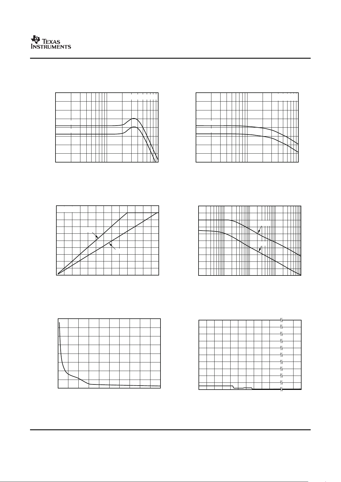
TYPICAL CHARACTERISTICS
45
40
35
30
25
20
15
10
5
10k
100k
Gain(dB)
Frequency(Hz)
1M
C =1000pF
LOAD
G=14
G=20
45
40
35
30
25
20
15
10
5
10k
100k
Gain(dB)
Frequency(Hz)
1M
G=20
G=14
C =0pF
LOAD
140
130
120
110
100
90
80
70
60
50
40
10
100 1k 10k
Common-Modeand
P
ower
-SupplyRejection(dB)
Frequency(Hz)
100k
CMRR
PSR
20
18
16
14
12
10
8
6
4
2
0
0
100
200
300
400
500
600
700
V (V)
OUT
V (mV)
SENSE
800
900
1000
1100
1200
1300
20V/V
14V/V
V =18V
S
4.0
3.5
3.0
2.5
2.0
1.5
1.0
0.5
0
0
50
100
150 200
250 300
350
TotalOutputError
(%erroroftheidealoutputvalue)
V (mV)
SENSE
400 450
500
0.10
0.09
0.08
0.07
0.06
0.05
0.04
0.03
0.02
0.01
0
-16
-12
-8
-4 0
4 128
2016
OutputError(%)
Common-ModeVoltage(V)
... 76
80
INA270
INA271
SBOS381A – FEBRUARY 2007 – REVISED APRIL 2007
At TA= +25 ° C, VS= +12V, V
CM
= 12V, and V
SENSE
= 100mV, unless otherwise noted.
GAIN vs FREQUENCY GAIN vs FREQUENCY
Figure 1. Figure 2.
COMMON-MODE AND POWER-SUPPLY REJECTION
GAIN PLOT vs FREQUENCY
Figure 3. Figure 4.
TOTAL OUTPUT ERROR vs V
SENSE
OUTPUT ERROR vs COMMON-MODE VOLTAGE
Figure 5. Figure 6.
5
Submit Documentation Feedback
Page 6

www.ti.com
12
11
10
9
8
7
6
5
4
3
2
1
0
0
5
10
15
20
OutputVoltage(V)
OutputCurrent(mA)
25
30
V =12V
S
+25 C°
+25 C°
- °40 C
- °40 C
+125 C°
+125 C°
SourcingCurrent
V =3V
S
SourcingCurrent
Outputstageisdesigned
tosourcecurrent.Current
sinkingcapabilityis
approximately400 A.m
1000
900
800
700
600
500
400
300
200
100
0
0
1
2
3 4
5 6
7
I ( A)m
Q
OutputVoltage(V)
8 9
10
34
30
26
22
18
14
10
6
2.5
3.5
4.5 5.5 6.5
7.5 8.5 9.5
10.5
OutputShort-CircuitCurrent(mA)
SupplyVoltage (V)
11.5 17
18
-40 C°
+25 C°
+125 C°
875
775
675
575
475
375
275
175
-16
-12
-8
-4 0 4
8 12 16
20
I
( A)m
Q
V (V)
CM
76
80
V =0mV:
SENSE
V =12V
S
V =2.7V
S
V =100mV:
SENSE
V =12V
S
V =2.7V
S
...
Frequency(Hz)
Gain(dB)
200
150
100
50
0
-50
10 100 1k 10k 100k 1M 10M
Phase
Gain
Population
R (k )W
PREOUT
80
82
84
86
88
90
92
94
96
98
100
102
104
106
108
110
112
114
116
118
120
INA270
INA271
SBOS381A – FEBRUARY 2007 – REVISED APRIL 2007
TYPICAL CHARACTERISTICS (continued)
At TA= +25 ° C, VS= +12V, V
CM
= 12V, and V
SENSE
= 100mV, unless otherwise noted.
POSITIVE OUTPUT VOLTAGE SWING QUIESCENT CURRENT
vs OUTPUT CURRENT vs OUTPUT VOLTAGE
Figure 7. Figure 8.
QUIESCENT CURRENT OUTPUT SHORT-CIRCUIT CURRENT
vs COMMON-MODE VOLTAGE vs SUPPLY VOLTAGE
Figure 9. Figure 10.
PREOUT OUTPUT RESISTANCE
PRODUCTION DISTRIBUTION BUFFER GAIN vs FREQUENCY
Figure 11. Figure 12.
6
Submit Documentation Feedback
Page 7

www.ti.com
50mV/div
10 s/divm
500mV/div
10 s/divm
INA270
INA271
SBOS381A – FEBRUARY 2007 – REVISED APRIL 2007
TYPICAL CHARACTERISTICS (continued)
At TA= +25 ° C, VS= +12V, V
CM
= 12V, and V
SENSE
= 100mV, unless otherwise noted.
SMALL-SIGNAL STEP RESPONSE LARGE-SIGNAL STEP RESPONSE
10mV TO 20mV INPUT 10mV TO 100mV INPUT
Figure 13. Figure 14.
7
Submit Documentation Feedback
Page 8

www.ti.com
APPLICATIONS INFORMATION
BASIC CONNECTION POWER SUPPLY
SELECTING R
S
A1
A2
Single-PoleFilter
Capacitor
+2.7Vto+18V
5kW5kW
96kW
R
L
PREOUT BUFIN
GND
OUT
IN-IN+ V+
Load
-16Vto+80V
Supply
R
S
INA270
0.01 Fm
0.1 Fm
INA270
INA271
SBOS381A – FEBRUARY 2007 – REVISED APRIL 2007
Figure 15 shows the basic connection of the INA270 The input circuitry of the INA270 and INA271 can
and INA271. The input pins, IN+ and IN–, should be accurately measure beyond its power-supply voltage,
connected as closely as possible to the shunt V+. For example, the V+ power supply can be 5V,
resistor to minimize any resistance in series with the whereas the load power-supply voltage is up to
shunt resistance. +80V. The output voltage range of the OUT terminal,
however, is limited by the voltages on the
Power-supply bypass capacitors are required for
power-supply pin.
stability. Applications with noisy or high-impedance
power supplies may require additional decoupling
capacitors to reject power-supply noise. Minimum
bypass capacitors of 0.01 µ F and 0.1 µ F in value
The value chosen for the shunt resistor, RS, depends
should be placed close to the supply pins. Although
on the application and is a compromise between
not mandatory, an additional 10mF electrolytic
small-signal accuracy and maximum permissible
capacitor placed in parallel with the other bypass
voltage loss in the measurement line. High values of
capacitors may be useful in applications with
R
S
provide better accuracy at lower currents by
particularly noisy supplies.
minimizing the effects of offset, while low values of
R
S
minimize voltage loss in the supply line. For most
applications, best performance is attained with an R
S
value that provides a full-scale shunt voltage range
of 50mV to 100mV. Maximum input voltage for
accurate measurements is (V
S
– 0.2)/Gain.
Figure 15. INA270 Basic Connections
8
Submit Documentation Feedback
Page 9

www.ti.com
TRANSIENT PROTECTION
OUTPUT VOLTAGE RANGE
a)Single-PoleFilter b)Second-Order,Sallen-KeyFilter
A1
A2
Single-PoleFilter
Capacitor
+2.7Vto+18V
5kW5kW
96kW
R
L
PREOUT BUFIN
GND
Output
IN-IN+ V+
Load
Supply
R
S
INA270
A1
A2
Second-Order,Sallen-KeyFilterConnection
+2.7Vto+18V
C
FILT
C
FILT
5kW5kW
96kW
R
L
PREOUT BUFIN
GND
Output
IN-IN+ V+
Load
Supply
R
S
R
S
INA270
INA270
INA271
SBOS381A – FEBRUARY 2007 – REVISED APRIL 2007
Despite the use of internal zener-type ESD
protection, the INA270 and INA271 are not suited to
The –16V to +80V common-mode range of the
using external resistors in series with the inputs since
INA270 and INA271 is ideal for withstanding
the internal gain resistors can vary up to ± 30%, but
automotive fault conditions ranging from 12V battery
are tightly matched (if gain accuracy is not important,
reversal up to +80V transients, since no additional
then resistors can be added in series with the
protective components are needed up to those
INA270 and INA271 inputs with two equal resistors
levels. In the event that the INA270 and INA271 are
on each input).
exposed to transients on the inputs in excess of their
ratings, external transient absorption with
semiconductor transient absorbers (zeners or
Transzorbs) will be necessary.
The output of the INA270 and INA271 is accurate
within the output voltage swing range set by the
Use of MOVs or VDRs is not recommended except
power-supply pin, V+.
when they are used in addition to a semiconductor
transient absorber. Select the transient absorber
The INA270 and INA271 readily enable the inclusion
such that it will never allow the INA270 and INA271
of filtering between the preamp output and buffer
to be exposed to transients greater than 80V (that is,
input. Single-pole filtering can be accomplished with
allow for transient absorber tolerance, as well as
a single capacitor because of the 96k Ω output
additional voltage because of transient absorber
impedance at PRE OUT on pin 3, as shown in
dynamic impedance).
Figure 16 a.
The INA270 and INA271 readily lend themselves to
second-order Sallen-Key configurations, as shown in
Figure 16 b. When designing these configurations
consider that the PRE OUT 96k Ω output impedance
exhibits an initial variation of ± 30% with the addition
of a –2200ppm/ ° C temperature coefficient.
Figure 16. The INA270–INA271 can be easily connected for first- or second-order filtering. Remember to
use the appropriate buffer gain (INA270 = 1.4, INA271 = 2) when designing Sallen-Key configurations.
9
Submit Documentation Feedback
Page 10

www.ti.com
Normal Case 2: V
SENSE
≥ 20mV, V
CM
< V
S
ACCURACY VARIATIONS AS A RESULT OF
Low V
SENSE
Case 1:
Normal Case 1: V
SENSE
≥ 20mV, V
CM
≥ V
S
G=
V V-
OUT1 OUT2
100mV 20mV-
(1)
V RTI(Referred-To-Input)=
OS
V
OUT1
G
- 100mV
(2)
2.0
1.8
1.6
1.4
1.2
1.0
0.8
0.6
0.4
0.2
0
0
2
4 6 8
10 12 14 16 18
V (V)
OUT
V (mV)
SENSE
20
Actual
Ideal
INA270
INA271
SBOS381A – FEBRUARY 2007 – REVISED APRIL 2007
V
SENSE
AND COMMON-MODE VOLTAGE
This region of operation has slightly less accuracy
than Normal Case 1 as a result of the common-mode
The accuracy of the INA270 and INA271 current
operating area in which the part functions, as seen in
shunt monitors is a function of two main variables:
the Output Error vs Common-Mode Voltage curve
V
SENSE
(V
IN+
– V
IN–
) and common-mode voltage,
(Figure 6 ). As noted, for this graph V
S
= 12V; for V
CM
V
CM
, relative to the supply voltage, VS. V
CM
is
< 12V, the Output Error increases as V
CM
becomes
expressed as (V
IN+
+ V
IN–
)/2; however, in practice,
less than 12V, with a typical maximum error of
V
CM
is seen as the voltage at V
IN+
because the
0.005% at the most negative V
CM
= –16V.
voltage drop across V
SENSE
is usually small.
This section addresses the accuracy of these
specific operating regions: V
SENSE
< 20mV, –16V ≤ V
CM
< 0; and
Low V
SENSE
Case 3:
Normal Case 1: V
SENSE
≥ 20mV, V
CM
≥ V
S
V
SENSE
< 20mV, VS< V
CM
≤ 80V
Normal Case 2: V
SENSE
≥ 20mV, V
CM
< V
S
Although the INA270 family of devices are not
Low V
SENSE
Case 1:
designed for accurate operation in either of these
V
SENSE
< 20mV, –16V ≤ V
CM
< 0
regions, some applications are exposed to these
Low V
SENSE
Case 2:
conditions. For example, when monitoring power
V
SENSE
< 20mV, 0V ≤ V
CM
≤ V
S
supplies that are switched on and off while V
S
is still
applied to the INA270 or INA271, it is important to
Low V
SENSE
Case 3:
know what the behavior of the devices will be in
V
SENSE
< 20mV, V
S
< V
CM
≤ 80V
these regions.
As V
SENSE
approaches 0mV, in these V
CM
regions,
the device output accuracy degrades. A
This region of operation provides the highest
larger-than-normal offset can appear at the current
accuracy. Here, the input offset voltage is
shunt monitor output with a typical maximum value of
characterized and measured using a two-step
V
OUT
= 60mV for V
SENSE
= 0mV. As V
SENSE
method. First, the gain is determined by Equation 1 .
approaches 20mV, V
OUT
returns to the expected
output value with accuracy as specified in the
Electrical Characteristics . Figure 17 shows this effect
using the INA271 (Gain = 20).
where:
V
OUT1
= Output Voltage with V
SENSE
= 100mV
V
OUT2
= Output Voltage with V
SENSE
= 20mV
Then the offset voltage is measured at V
SENSE
=
100mV and referred to the input (RTI) of the current
shunt monitor, as shown in Equation 2 .
In the Typical Characteristics , the Output Error vs
Common-Mode Voltage curve (Figure 6 ) shows the
highest accuracy for the this region of operation. In
this plot, V
S
= 12V; for V
CM
≥ 12V, the output error is
at its minimum. This case is also used to create the
V
SENSE
≥ 20mV output specifications in the Electrical
Characteristics table.
Figure 17. Example for Low V
SENSE
Cases 1 and 3
(INA271, Gain = 20)
10
Submit Documentation Feedback
Page 11

www.ti.com
Low V
SENSE
Case 2: V
SENSE
< 20mV, 0V ≤ V
CM
≤ V
S
SHUTDOWN
RFI/EMI
0.48
0.48
0.40
0.36
0.32
0.28
0.24
0.20
0.16
0.12
0.08
0.04
0
0
2
4 6 8
10 12 14 16 18 20 22
V
(V)
O
UT
V (mV)
SENSE
24
INA271V
OUT
Limit
(1)
V
CM2
V
CM1
V
CM3
V
CM4
V ,V
CM2
CM3
CM4
,andV illustratethevariance
fromparttopartoftheV thatcancauseCM
maximumV withV <20mV.
OUT SENSE
V limitatV =0mV,
OUT SENSE
0 V£
CM1 S
£ V
NOTE:(1)INA271V Limit=0.4V.INA270V Limit=0.28V.
OUT OUT
Ideal
INA270
INA271
SBOS381A – FEBRUARY 2007 – REVISED APRIL 2007
This region of operation is the least accurate for the
The INA270 and INA271 do not provide a shutdown
INA270 family. To achieve the wide input
pin; however, because they consume a quiescent
common-mode voltage range, these devices use two
current less than 1mA, they can be powered by
op amp front ends in parallel. One op amp front end
either the output of logic gates or by transistor
operates in the positive input common-mode voltage
switches to supply power. Driving the gate low shuts
range, and the other in the negative input region. For
down the INA270–INA271. Use a totem-pole output
this case, neither of these two internal amplifiers
buffer or gate that can provide sufficient drive along
dominates and overall loop gain is very low. Within
with 0.1 µ F bypass capacitor, preferably ceramic with
this region, V
OUT
approaches voltages close to linear
good high-frequency characteristics. This gate
operation levels for Normal Case 2.
should have a supply voltage of 3V or greater
because the INA270 and INA271 require a minimum
This deviation from linear operation becomes
supply greater than 2.7V. In addition to eliminating
greatest the closer V
SENSE
approaches 0V. Within
quiescent current, this gate also turns off the 10 µ A
this region, as V
SENSE
approaches 20mV, device
bias current present at each of the inputs. Note that
operation is closer to that described by Normal Case
the IN+ and IN– inputs are able to withstand full
2. Figure 18 illustrates this behavior for the INA271.
common-mode voltage under all powered and
The V
OUT
maximum peak for this case is determined
under-powered conditions. An example shutdown
by maintaining a constant VS, setting V
SENSE
= 0mV,
circuit is illustrated in Figure 19 .
and sweeping V
CM
from 0V to VS. The exact V
CM
at
which V
OUT
peaks during this case varies from part to
part. The maximum peak voltage for the INA270 is
0.28V; for the INA271, the maximum peak voltage is
Attention to good layout practices is always
0.4V.
recommended. Keep traces short and, when
possible, use a printed circuit board (PCB) ground
plane with surface-mount components placed as
close to the device pins as possible. Small ceramic
capacitors placed directly across amplifier inputs can
reduce RFI/EMI sensitivity. PCB layout should locate
the amplifier as far away as possible from RFI
sources. Sources can include other components in
the same system as the amplifier itself, such as
inductors (particularly switched inductors handling a
lot of current and at high frequencies). RFI can
generally be identified as a variation in offset voltage
or dc signal levels with changes in the interfering RF
signal. If the amplifier cannot be located away from
sources of radiation, shielding may be needed.
Twisting wire input leads makes them more resistant
to RF fields. The difference in input pin location of
the INA270 and INA271 versus the INA193–INA198
may provide different EMI performance.
Figure 18. Example for Low V
SENSE
Case 2
(INA271, Gain = 20)
11
Submit Documentation Feedback
Page 12

www.ti.com
R
S
0.1 Fm
V+>3V
Load
-16Vto+80V
Supply
Negative
and
Positive
Common-Mode
Voltage
I
L
A1
A2
Single-PoleFilter
Capacitor
5kW5kW
96kW
R
L
PREOUT BUFIN
GND
OUT
IN-IN+ V+
INA270,INA271
74HC04
INA270
INA271
SBOS381A – FEBRUARY 2007 – REVISED APRIL 2007
Figure 19. INA270–INA271 Example Shutdown Circuit
12
Submit Documentation Feedback
Page 13

PACKAGING INFORMATION
Orderable Device Status
(1)
Package
Type
Package
Drawing
Pins Package
Qty
Eco Plan
(2)
Lead/Ball Finish MSL Peak Temp
(3)
INA270AID ACTIVE SOIC D 8 75 Green (RoHS &
no Sb/Br)
CU NIPDAU Level-1-260C-UNLIM
INA270AIDR ACTIVE SOIC D 8 2500 Green (RoHS &
no Sb/Br)
CU NIPDAU Level-1-260C-UNLIM
INA271AID ACTIVE SOIC D 8 75 Green (RoHS &
no Sb/Br)
CU NIPDAU Level-1-260C-UNLIM
INA271AIDR ACTIVE SOIC D 8 2500 Green (RoHS &
no Sb/Br)
CU NIPDAU Level-1-260C-UNLIM
(1)
The marketing status values are defined as follows:
ACTIVE: Product device recommended for new designs.
LIFEBUY: TI has announced that the device will be discontinued, and a lifetime-buy period is in effect.
NRND: Not recommended for new designs. Device is in production to support existing customers, but TI does not recommend using this part in
a new design.
PREVIEW: Device has been announced but is not in production. Samples may or may not be available.
OBSOLETE: TI has discontinued the production of the device.
(2)
Eco Plan - The planned eco-friendly classification: Pb-Free (RoHS), Pb-Free (RoHS Exempt), or Green (RoHS & no Sb/Br) - please check
http://www.ti.com/productcontent for the latest availability information and additional product content details.
TBD: The Pb-Free/Green conversion plan has not been defined.
Pb-Free (RoHS): TI's terms "Lead-Free" or "Pb-Free" mean semiconductor products that are compatible with the current RoHS requirements
for all 6 substances, including the requirement that lead not exceed 0.1% by weight in homogeneous materials. Where designed to be soldered
at high temperatures, TI Pb-Free products are suitable for use in specified lead-free processes.
Pb-Free (RoHS Exempt): This component has a RoHS exemption for either 1) lead-based flip-chip solder bumps used between the die and
package, or 2) lead-based die adhesive used between the die and leadframe. The component is otherwise considered Pb-Free (RoHS
compatible) as defined above.
Green (RoHS & no Sb/Br): TI defines "Green" to mean Pb-Free (RoHS compatible), and free of Bromine (Br) and Antimony (Sb) based flame
retardants (Br or Sb do not exceed 0.1% by weight in homogeneous material)
(3)
MSL, Peak Temp. -- The Moisture Sensitivity Level rating according to the JEDEC industry standard classifications, and peak solder
temperature.
Important Information and Disclaimer:The information provided on this page represents TI's knowledge and belief as of the date that it is
provided. TI bases its knowledge and belief on information provided by third parties, and makes no representation or warranty as to the
accuracy of such information. Efforts are underway to better integrate information from third parties. TI has taken and continues to take
reasonable steps to provide representative and accurate information but may not have conducted destructive testing or chemical analysis on
incoming materials and chemicals. TI and TI suppliers consider certain information to be proprietary, and thus CAS numbers and other limited
information may not be available for release.
In no event shall TI's liability arising out of such information exceed the total purchase price of the TI part(s) at issue in this document sold by TI
to Customer on an annual basis.
PACKAGE OPTION ADDENDUM
www.ti.com
30-Mar-2007
Addendum-Page 1
Page 14

Page 15

IMPORTANT NOTICE
Texas Instruments Incorporated and its subsidiaries (TI) reserve the right to make corrections, modifications,
enhancements, improvements, and other changes to its products and services at any time and to
discontinue any product or service without notice. Customers should obtain the latest relevant information
before placing orders and should verify that such information is current and complete. All products are sold
subject to TI’s terms and conditions of sale supplied at the time of order acknowledgment.
TI warrants performance of its hardware products to the specifications applicable at the time of sale in
accordance with TI’s standard warranty. Testing and other quality control techniques are used to the extent
TI deems necessary to support this warranty. Except where mandated by government requirements, testing
of all parameters of each product is not necessarily performed.
TI assumes no liability for applications assistance or customer product design. Customers are responsible
for their products and applications using TI components. To minimize the risks associated with customer
products and applications, customers should provide adequate design and operating safeguards.
TI does not warrant or represent that any license, either express or implied, is granted under any TI patent
right, copyright, mask work right, or other TI intellectual property right relating to any combination, machine,
or process in which TI products or services are used. Information published by TI regarding third-party
products or services does not constitute a license from TI to use such products or services or a warranty or
endorsement thereof. Use of such information may require a license from a third party under the patents or
other intellectual property of the third party, or a license from TI under the patents or other intellectual
property of TI.
Reproduction of information in TI data books or data sheets is permissible only if reproduction is without
alteration and is accompanied by all associated warranties, conditions, limitations, and notices.
Reproduction of this information with alteration is an unfair and deceptive business practice. TI is not
responsible or liable for such altered documentation.
Resale of TI products or services with statements different from or beyond the parameters stated by TI for
that product or service voids all express and any implied warranties for the associated TI product or service
and is an unfair and deceptive business practice. TI is not responsible or liable for any such statements.
Following are URLs where you can obtain information on other Texas Instruments products and application
solutions:
Products
Applications
Amplifiers amplifier.ti.com Audio www.ti.com/audio
Data Converters dataconverter.ti.com Automotive www.ti.com/automotive
DSP dsp.ti.com Broadband www.ti.com/broadband
Interface interface.ti.com Digital Control www.ti.com/digitalcontrol
Logic logic.ti.com Military www.ti.com/military
Power Mgmt power.ti.com Optical Networking www.ti.com/opticalnetwork
Microcontrollers microcontroller.ti.com Security www.ti.com/security
Low Power Wireless www.ti.com/lpw Telephony www.ti.com/telephony
Video & Imaging www.ti.com/video
Wireless www.ti.com/wireless
Mailing Address: Texas Instruments
Post Office Box 655303 Dallas, Texas 75265
Copyright © 2007, Texas Instruments Incorporated
 Loading...