

®
INA209
Critical
DAC+
Critical
DAC -
´
CMP
Filter
OverlimitRegister
WarningRegister
PowerRegister
CurrentRegister
I C
Interface
2
VoltageRegister
ConvertGND GPIO
V
IN+VIN-
V
S
(SupplyVoltage)
Critical
Overlimit
Warning
Alert
Data
CLK
CMP
ADC
High-Side Measurement, Bi-Directional Current/Power Monitor
with I2C™ Interface
FEATURES DESCRIPTION
• SENSES BUS VOLTAGES FROM 0V TO +26V
• REPORTS CURRENT, VOLTAGE, AND
POWER; STORES PEAKS
• TRIPLE WATCHDOG LIMITS:
– Lower Warning with Delay
– Upper Over-limit, No Delay
– Fast Analog Critical
• HIGH ACCURACY: 1% MAX OVER TEMP
APPLICATIONS
• SERVERS
• TELECOM EQUIPMENT
• AUTOMOTIVE The INA209 also includes an analog-to-digital
• POWER MANAGEMENT
• BATTERY CHARGERS
• WELDING EQUIPMENT
• POWER SUPPLIES
• TEST EQUIPMENT
The INA209 is a high-side current shunt and power
monitor with an I2C interface. The INA209 monitors
both shunt drop and shunt bus voltage. A
programmable calibration value, combined with an
internal multiplier, enables direct readouts in
amperes. An additional multiplying register calculates
power in watts. The INA209 features two separate,
onboard watchdog capabilities: a warning
comparator and an over-limit comparator. The
warning comparator is useful for monitoring lower
warning limits and incorporates a user-defined delay.
The over-limit comparator assists with monitoring
upper limits that could require immediate system
shutdown.
converter (ADC) comparator and a programmable
digital-to-analog converter (DAC) that combine to
provide the fastest possible responses to current
overload conditions.
The INA209 can be used together with hot swap
controllers that already use a current sense resistor.
The INA209 full-scale range can be selected to be
either within the hot-swap controller sense limits, or
wide enough to include them.
INA209
SBOS403 – JUNE 2007
I2C is a trademark of NXP Semiconductors.
All other trademarks are the property of their respective owners.
PRODUCTION DATA information is current as of publication date.
Products conform to specifications per the terms of the Texas
Instruments standard warranty. Production processing does not
necessarily include testing of all parameters.
Please be aware that an important notice concerning availability, standard warranty, and use in critical applications of Texas
Instruments semiconductor products and disclaimers thereto appears at the end of this data sheet.
The INA209 senses across shunts on buses that can
vary from 0V to 26V. The device uses a single +3V
to +5.5V supply, drawing a maximum of 1.5mA of
supply current. It is specified for operation from
–25 ° C to +85 ° C.
Copyright © 2007, Texas Instruments Incorporated
www.ti.com
INA209
SBOS403 – JUNE 2007
This integrated circuit can be damaged by ESD. Texas Instruments recommends that all integrated circuits be handled with
appropriate precautions. Failure to observe proper handling and installation procedures can cause damage.
ESD damage can range from subtle performance degradation to complete device failure. Precision integrated circuits may be
more susceptible to damage because very small parametric changes could cause the device not to meet its published
specifications.
ORDERING INFORMATION
(1)
PRODUCT PACKAGE-LEAD PACKAGE DESIGNATOR PACKAGE MARKING
INA209 TSSOP-16 PW INA209A
(1) For the most current package and ordering information see the Package Option Addendum at the end of this document, or see the TI
web site at www.ti.com .
ABSOLUTE MAXIMUM RATINGS
(1)
Over operating free-air temperature range (unless otherwise noted).
INA209 UNIT
Supply Voltage, V
Analog Inputs,
V
, V
IN+
IN–
S
Differential (V
) – (V
IN+
(2)
)
IN–
Common-Mode –0.3 to +26 V
Open-Drain Digital Outputs GND – 0.3 to +6 V
GPIO, Convert Pins GND – 0.3 to VS+ 0.3 V
Input Current Into Any Pin 5 mA
Open-Drain Digital Output Current 10 mA
Operating Temperature –40 to +125 ° C
Storage Temperature –40 to +150 ° C
Junction Temperature +150 ° C
Human Body Model 2000 V
ESD Ratings Charged-Device Model 1000 V
Machine Model (MM) 150 V
(1) Stresses above these ratings may cause permanent damage. Exposure to absolute maximum conditions for extended periods may
degrade device reliability. These are stress ratings only, and functional operation of the device at these or any other conditions beyond
those specified is not implied.
(2) V
and V
IN+
+26V.
may have a differential voltage of –26V to +26V; however, the voltage at these pins must not exceed the range –0.3V to
IN–
6 V
–26 to +26 V
2
Submit Documentation Feedback

www.ti.com
SBOS403 – JUNE 2007
INA209
ELECTRICAL CHARACTERISTICS: V
Boldface limits apply over the specified temperature range, TA= –25 ° C to +85 ° C.
At TA= +25 ° C, V
INPUT
Full-Scale Current Sense (Input) Voltage Range PGA = ÷ 1 0 ± 40 mV
Bus Voltage (Input Voltage) Range
Common-Mode Rejection CMRR V
Offset Voltage, RTI
vs Temperature 0.1 µ V/ ° C
vs Power Supply PSRR VS= 3V to 5.5V 10 µ V/V
Current Sense Gain Error ± 40 m%
vs Temperature 10 ppm/ ° C
Input Impedance Active Mode
V
Pin 20 µ A
IN+
V
Pin 20 || 320 µ A || k Ω
IN–
Input Leakage Power-Down Mode
V
Pin 0.1 ± 0.5 µ A
IN+
V
Pin 0.1 ± 0.5 µ A
IN–
DC ACCURACY
ADC Basic Resolution 12 Bits
1 LSB Step Size
Shunt Voltage 10 µ V
Bus Voltage 4 mV
Current Measurement Error ± 0.2 ± 0.5 %
over Temperature ± 1 %
Bus Voltage Measurement Error ± 0.2 ± 0.5 %
over Temperature ± 1 %
Differential Nonlinearity ± 0.1 LSB
Critical DAC Full-Scale Range 255 mV
Critical DAC Accuracy ± 0.5 ± 1 %
Critical DAC Resolution 8 Bits
Critical DAC 1 LSB Step Size 1 mV
Critical DAC Comparator Offset ± 0.3 ± 1.6 mV
Critical DAC Comparator Hysteresis
Critical DAC Comparator Delay 5 µ s
= 12V, V
IN+
PARAMETER TEST CONDITIONS MIN TYP MAX UNIT
(3)
= (V
SENSE
(2)
(4)
– V
IN+
= +3.3V
S
) = 32mV, PGA = ÷ 1, and BRNG
IN–
IN+
V
OS
(1)
= 1, unless otherwise noted.
INA209
PGA = ÷ 2 0 ± 80 mV
PGA = ÷ 4 0 ± 160 mV
PGA = ÷ 8 0 ± 320 mV
BRNG = 1 0 32 V
BRNG = 0 0 16 V
= 0V to 26V 100 120 dB
PGA = ÷ 1 ± 10 ± 100 µ V
PGA = ÷ 2 ± 20 ± 125 µ V
PGA = ÷ 4 ± 30 ± 150 µ V
PGA = ÷ 8 ± 40 ± 200 µ V
(4)
See
(1) BRNG is bit 13 of the Configuration Register.
(2) This parameter only expresses the full-scale range of the ADC scaling. In no event should more than 26V be applied to this device.
(3) Referred-to-input (RTI).
(4) User-programmable. See the Critical Comparator and Register sections.
Submit Documentation Feedback
3

www.ti.com
INA209
SBOS403 – JUNE 2007
ELECTRICAL CHARACTERISTICS: V
= +3.3V (continued)
S
Boldface limits apply over the specified temperature range, TA= –25 ° C to +85 ° C.
At TA= +25 ° C, V
ADC TIMING
ADC Conversion Time 12-Bit 532 586 µ s
Minimum Convert Input Low Time 4 µ s
SMBus
SMBus Timeout
DIGITAL INPUTS
(Convert, GPIO and SDA as Input, SCL, A0, A1)
Input Capacitance Leakage 3 pF
Input Current 0 ≤ VIN≤ V
Input Logic Levels:
V
IH
V
IL
Hysteresis 500 mV
DIGITAL OUTPUTS
GPIO Pin Output Low I
GPIO Pin Output High I
OPEN-DRAIN DIGITAL OUTPUTS
(Critical, Over-Limit, Warning, Alert, SDA)
Logic '0' Output Level I
High-Level Output Leakage Current V
POWER SUPPLY
Operating Supply Range +3 +5.5 V
Quiescent Current 1 1.5 mA
Quiescent Current, Power-Down Mode 6 15 µ A
Power-On Reset Threshold 2 V
TEMPERATURE RANGE
Specified Temperature Range –25 +85 ° C
Operating Temperature Range –40 +125 ° C
Thermal Resistance θ
TSSOP-16 +150 ° C/W
= 12V, V
IN+
PARAMETER TEST CONDITIONS MIN TYP MAX UNIT
(5)
= (V
– V
SENSE
IN+
) = 32mV, PGA = ÷ 1, and BRNG = 1, unless otherwise noted.
IN–
11-Bit 276 304 µ s
10-Bit 148 163 µ s
9-Bit 84 93 µ s
S
0.7 (VS) 6 V
–0.3 0.3 (VS) V
= 3mA 0.15 0.4 V
SINK
= 3mA VS– 0.4 VS– 0.15 V
SOURCE
= 3mA 0.15 0.4 V
SINK
= V
OUT
S
JA
INA209
28 35 ms
0.1 1 µ A
0.1 1 µ A
(5) SMBus timeout in the INA209 resets the interface any time SCL is low for over 28ms.
4
Submit Documentation Feedback
www.ti.com
1
2
3
4
5
6
7
8
16
15
14
13
12
11
10
9
SMBusAlert
A1
A0
SDA
SCL
GND
V
S+
Warning
V
IN+
V
IN-
Convert
GND
V
S+
GPIO
Critical
Overlimit
SBOS403 – JUNE 2007
PIN CONFIGURATIONS
INA209
Top View
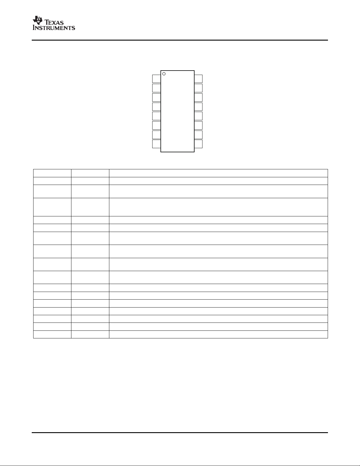
PIN DESCRIPTIONS
PIN NO. NAME DESCRIPTION
1 V
2 V
IN+
IN–
3 Convert Used to trigger conversions in triggered mode. In triggered mode, this pin should normally be high and
4 GND Connect together with pin 11 to ground.
5 V
S+
6 GPIO General-purpose, user-programmable input/output. Totem-pole output. Connect to ground or supply if
7 Critical Open-drain critical watchdog output (filter set in Critical DAC– Register). Default condition is disabled;
8 Overlimit Open-drain over-limit watchdog output. Default condition is disabled; active-low; transparent
9 Warning Open-drain warning watchdog output (delay set in Critical DAC– Register). Default condition is
10 V
S+
11 GND Connect together with pin 4 to ground.
12 SCL Serial bus clock line.
13 SDA Serial bus data line.
14 A0 Address pin. Table 1 shows pin settings and corresponding addresses.
15 A1 Address pin. Table 1 shows pin settings and corresponding addresses.
16 SMBus Alert Open-drain SMBus alert output. Controlled in SMBus Alert Mask Register. Default is disabled.
Positive differential shunt voltage. Connect to positive side of shunt resistor.
Negative differential shunt voltage. Connect to negative side of shunt resistor. Bus voltage is
measured from this pin to ground.
taken low to initiate conversion. It may be returned high after 4 µ s. If held low, the ADC converts each
time a triggered mode command is written via the I2C bus. If not used, this line should be tied high.
Connect together with pin 10 to supply, 3V to 5.5V.
not used. Default condition is as an input.
active-low; transparent (non-latched).
(non-latched).
disabled; active-low; transparent (non-latched).
Connect together with pin 5 to supply, 3V to 5.5V.
INA209
Submit Documentation Feedback
5
www.ti.com
0
-10
-20
-30
-40
-50
-60
-70
-80
-90
-100
10
100
1k
10k 100k
1M
Gain(dB)
InputFrequency(Hz)
100
80
60
40
20
0
-20
-40
-60
-80
-100
-40
-25
0
25 50
75 100
Offset( V)m
Temperature( C)°
125
160mVRange
320mVRange
80mVRange
40mVRange
100
80
60
40
20
0
-20
-40
-60
-80
-100
-40
-25
0
25 50
75 100
GainError(m%)
Temperature( C)°
125
320mVRange
160mVRange
80mVRange
40mVRange
50
45
40
35
30
25
20
15
10
5
0
-40
-25
0
25 50
75 100
Offset(mV)
Temperature( C)°
125
32VRange
16VRange
20
15
10
5
0
-5
-10
-15
-20
-0.4
-0.3
-0.2
-0.1 0
0.1 0.2 0.3
INL(
V)m
InputVoltage(V)
0.4
100
80
60
40
20
0
-20
-40
-60
-80
-100
-40
-25
0
25 50
75 100
GainError(m%)
Temperature( C)°
125
32VRange
16VRange
INA209
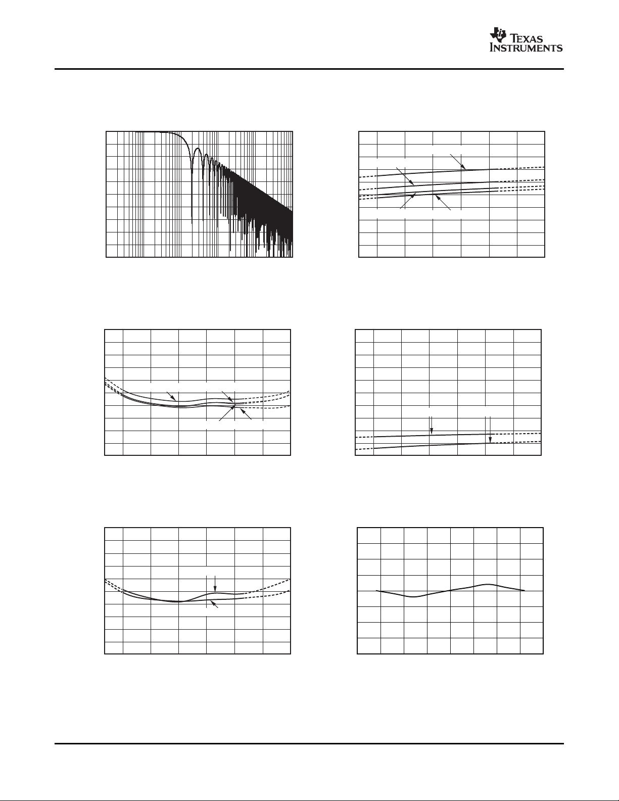
SBOS403 – JUNE 2007
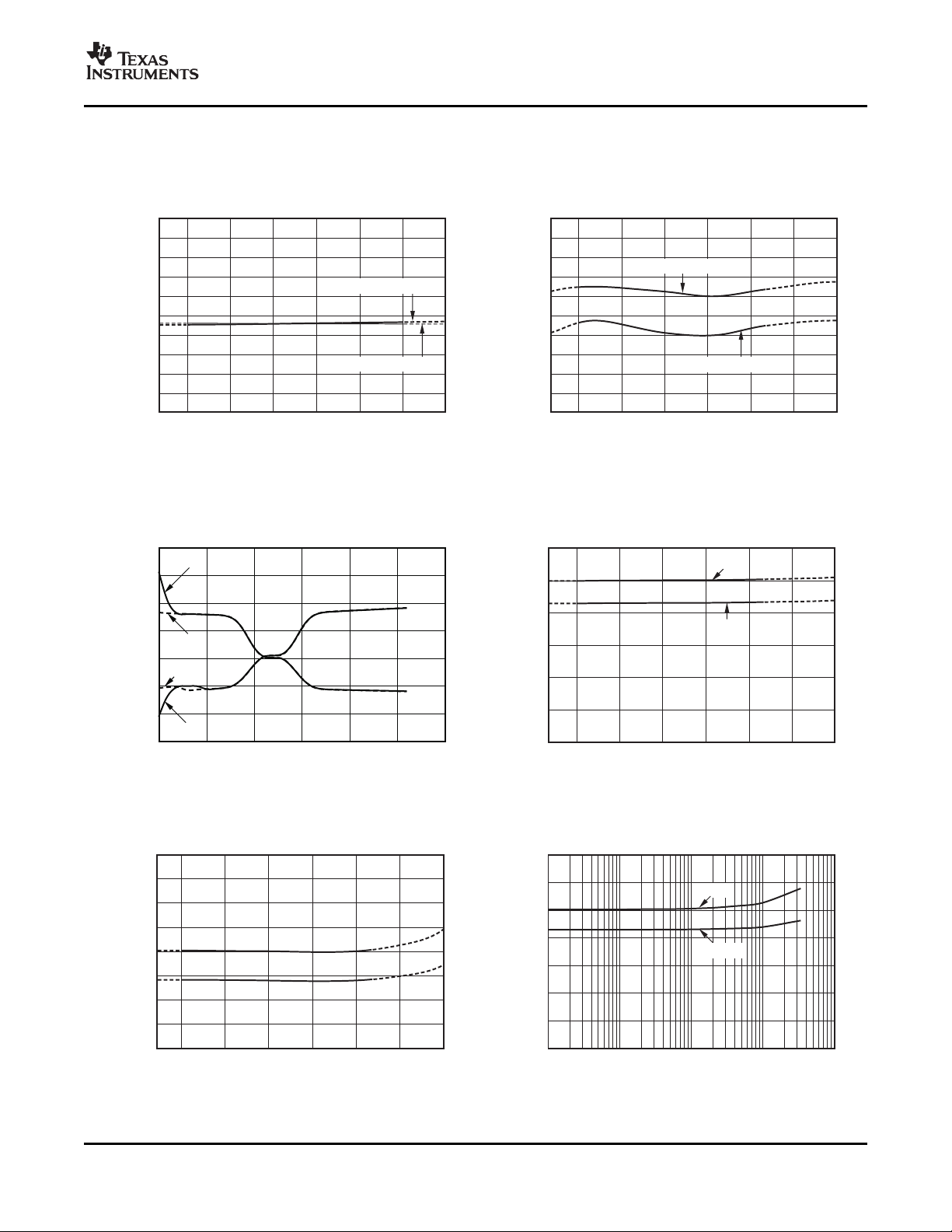
At TA= +25 ° C, V
TYPICAL CHARACTERISTICS
= 12V, V
IN+
FREQUENCY RESPONSE ADC SHUNT OFFSET vs TEMPERATURE
Figure 1. Figure 2.
= (V
– V
SENSE
IN+
) = 32mV, PGA = ÷ 1, and BRNG = 1, unless otherwise noted.
IN–
ADC SHUNT GAIN ERROR vs TEMPERATURE ADC BUS VOLTAGE OFFSET vs TEMPERATURE
Figure 3. Figure 4.
ADC BUS GAIN ERROR vs TEMPERATURE INTEGRAL NONLINEARITY vs INPUT VOLTAGE
6
Figure 5. Figure 6.
Submit Documentation Feedback
www.ti.com
1.0
0.8
0.6
0.4
0.2
0
-0.2
-0.4
-0.6
-0.8
-1.0
-40
-25
0
25 50
75 100
Offset(mV)
Temperature( C)°
125
CriticalComparator -
CriticalComparator+
1.0
0.8
0.6
0.4
0.2
0
-0.2
-0.4
-0.6
-0.8
-1.0
-40
-25
0
25 50
75 100
Full-ScaleError(mV)
Temperature( C)°
125
CriticalComparator -
CriticalComparator+
2.0
1.5
1.0
0.5
0
-0.5
-1.0
-1.5
0
5
10
15 20
25
InputCurrents(mA)
V Voltage(V)
IN-
30
VS+=5V
V 5VS+=
VS+=3V
V 3VS+=
1.2
1.0
0.8
0.6
0.4
0.2
0
-40
-25
0
25 50
75 100
I
(mA)
Q
Temperature( C)°
125
V =5V
S
V =3V
S
16
14
12
10
8
6
4
2
0
-40
-25
0
25
125
I ( A)m
Q
Temperature( C)°
V =5V
S
V =3V
S
50 75 100
1.4
1.2
1.0
0.8
0.6
0.4
0.2
0
1k
10k
100k
1M
10M
I
Q
(m
A)
SCLFrequency(Hz)
V =5V
S
V =S3V
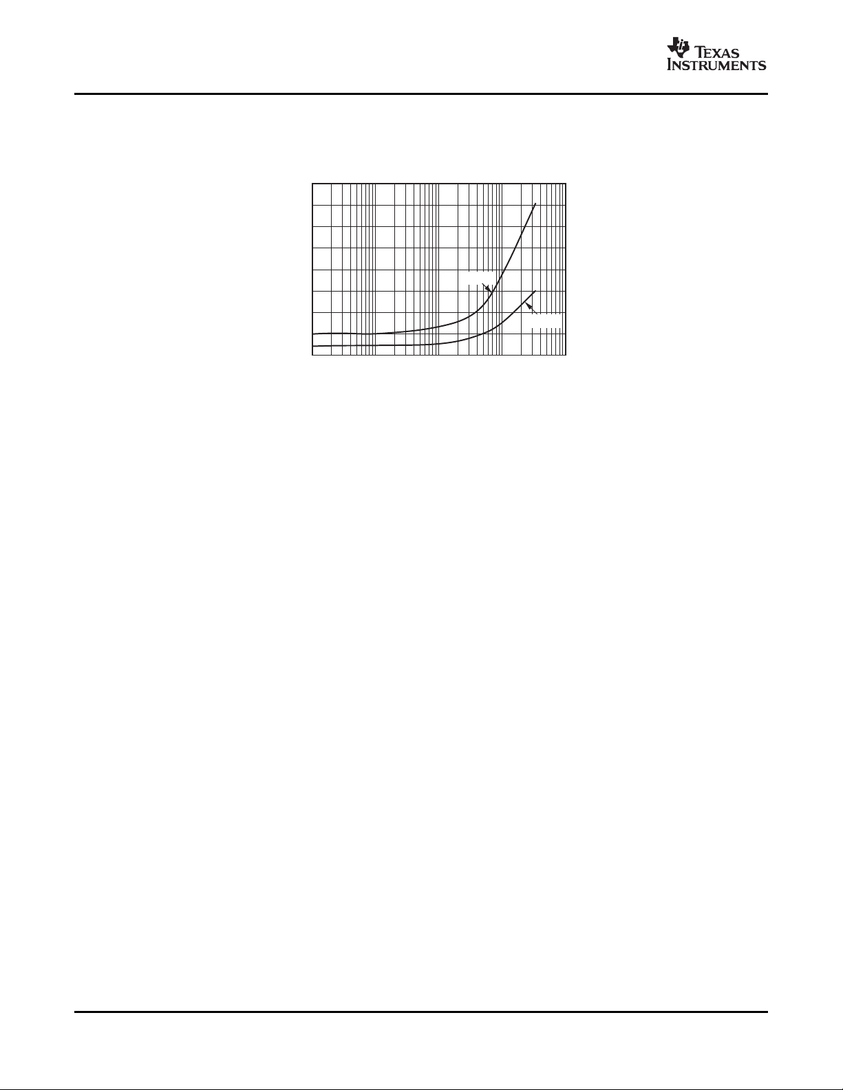
At TA= +25 ° C, V
IN+
= 12V, V
TYPICAL CHARACTERISTICS (continued)
= (V
SENSE
– V
IN+
) = 32mV, PGA = ÷ 1, and BRNG = 1, unless otherwise noted.
IN–
INA209
SBOS403 – JUNE 2007
CRITICAL COMPARATOR OFFSET vs TEMPERATURE TEMPERATURE
Figure 7. Figure 8.
INPUT CURRENTS WITH LARGE DIFFERENTIAL
VOLTAGES
(V
at 12V, Sweep of V
IN+
) ACTIVE IQvs TEMPERATURE
IN–
CRITICAL COMPARATOR FULL-SCALE ERROR vs
Figure 9. Figure 10.
SHUTDOWN IQvs TEMPERATURE ACTIVE IQvs I2C FREQUENCY
Figure 11. Figure 12.
Submit Documentation Feedback
7
www.ti.com
400
350
300
250
200
150
100
50
0
1k
10k
100k
1M
10M
I ( A)
Q
m
SCLFrequency(Hz)
V =5V
S
V =3V
S
INA209
SBOS403 – JUNE 2007
At TA= +25 ° C, V
IN+
= 12V, V
TYPICAL CHARACTERISTICS (continued)
= (V
SENSE
– V
IN+
) = 32mV, PGA = ÷ 1, and BRNG = 1, unless otherwise noted.
IN–
SHUTDOWN IQvs I2C FREQUENCY
Figure 13.
Submit Documentation Feedback
8
www.ti.com
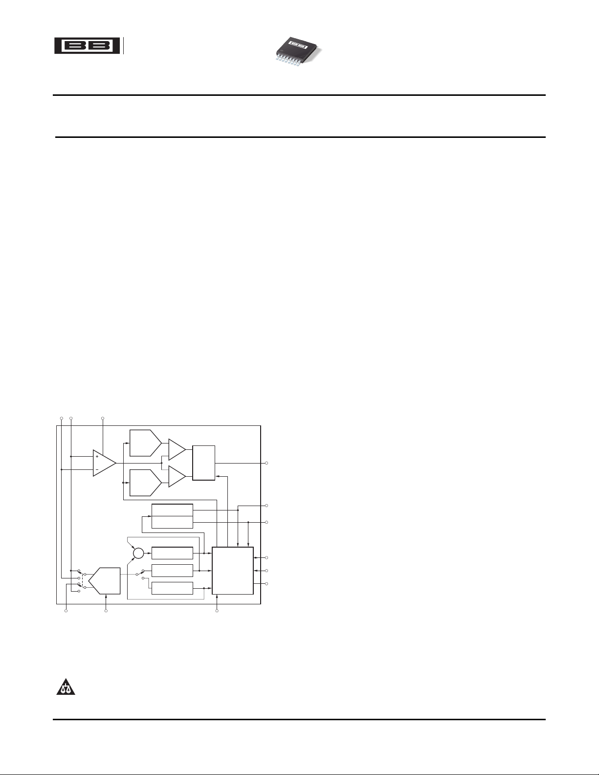
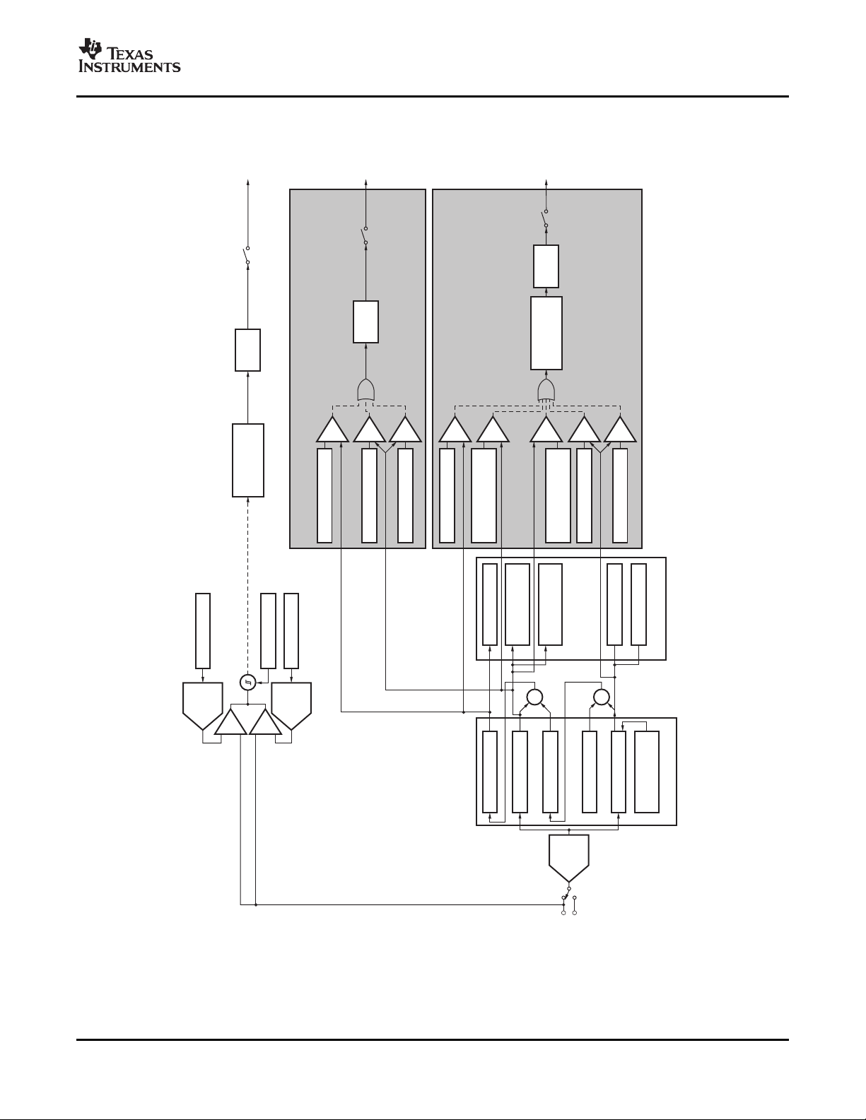
FUNCTIONAL BLOCK DIAGRAM
ADC
DAC
´
´
ShuntVoltage
Channel
BusV
oltage
Channel
PGA
(InConfigurationRegister)
ShuntVoltage
(1)
DataRegisters
Full-ScaleCalibration
(2)
Current
(1)
BusVoltage
(1)
Power
(1)
ShuntV
oltage Peak-
(2)
ShuntV
oltage+Peak
(2)
Peak-HoldRegisters
BusV
oltage
MinimumPeak
(2)
BusVoltage
MaximumPeak
(2)
PowerPeak
(2)
CMP
CMP
CMP
CMP
CMP
CMP
CMP
CMP
CMP
CMP
ShuntV
oltage Warning-
(2)
ShuntV
oltage+Warning
(2)
BusVoltageUnder-
VoltageWarning
(2)
ProgrammableDelay
(setin
CriticalDAC Register)-
Latchand
Polarity
BusV
oltageOver
-
VoltageWarning
(2)
PowerW
arning
(2)
BusUnder-Voltage Over-limit
(2)
BusOver-Voltage Over-limit
(2)
Power Over-limit
(2)
Enable/Disable
inSMBus/Enable
Register
W
arning
(Open-Drain)
Latchand
Polarity
Enable/Disable
inSMBus/Enable
Register
Over-limit
(Open-Drain)
WarningOutputDefault:
· Disabled
· ActiveLow
· Transparent(notlatched)
ProgrammableDelay
(setin
CriticalDAC Register)-
Latchand
Polarity
Enable/Disable
inSMBus/Enable
Register
Critical
(Open-Drain)
CriticalOutputDefault:
· Disabled
· ActiveLow
· Transparent(notlatched)
WarningRegistersandOutput
OverlimitOutputDefault:
·
Disabled
· ActiveLow
· Transparent(notlatched)
OverlimitRegistersandOutput
CriticalDAC+
(2)
DAC
CriticalDAC-
(2)
CriticalDACHysteresis
NOTE:DashedlineindicatestheflagisintheStatusRegister
.
(1)Read-only.
(2)Read/Write.
INA209
SBOS403 – JUNE 2007
Submit Documentation Feedback
Figure 14.
9
www.ti.com
PowerRegister
CurrentRegister
VoltageRegister
OverlimitRegister
WarningRegister
I C
Interface
2
GND
V
S
Supply
Voltage
V
IN-
V
IN+
Warning
Overlimit
CMP
Filter
Critical
V
I
Convert
Data
CLK
Alert
GPIO
Critical
DAC+
Critical
DAC-
Supply
Load
Current
Shunt
3.3VSupply
CriticalOutput
OverlimitOutput
WarningOutput
Data(SDA)
Clock(SCL)
C
0.1 F
BYPASS
m
CMP
INA209
SBOS403 – JUNE 2007
APPLICATION INFORMATION
The INA209 is a digital current-shunt monitor with an To address a specific device, the master initiates a
I2C and SMBus-compatible interface. It provides START condition by pulling the data signal line
digital current, voltage, and power readings (SDA) from a HIGH to a LOW logic level while SCL
necessary for accurate decision-making in is HIGH. All slaves on the bus shift in the slave
precisely-controlled systems. Programmable address byte on the rising edge of SCL, with the last
registers allow flexible configuration for setting bit indicating whether a read or write operation is
warning limits, measurement resolution, and intended. During the ninth clock pulse, the slave
continuous-versus-triggered operation. Detailed being addressed responds to the master by
register information appears at the end of this data generating an Acknowledge and pulling SDA LOW.
sheet, beginning with Table 2 . See the Functional
Block Diagram for a block diagram of the INA209.
The INA209 offers compatability with I2C and SMBus data transfer, SDA must remain stable while SCL is
interfaces. The I2C and SMBus protocols are HIGH. Any change in SDA while SCL is HIGH is
essentially compatible with each other. I2C will be interpreted as a START or STOP condition.
used throughout this document, with SMBus being
specified only when a difference between the two
systems is being addressed. Two bi-directional lines,
SCL and SDA, connect the INA209 to the bus. Both
SCL and SDA are open-drain connections. Figure 15
shows a typical application circuit.
Data transfer is then initiated and eight bits of data
are sent, followed by an Acknowledge bit. During
Once all data have been transferred, the master
generates a STOP condition, indicated by pulling
SDA from LOW to HIGH while SCL is HIGH. The
INA209 includes a 28ms timeout on its interface to
prevent locking up an SMBus.
BUS OVERVIEW
The device that initiates the transfer is called a
master, and the devices controlled by the master are
slaves. The bus must be controlled by a master
device that generates the serial clock (SCL), controls
the bus access, and generates START and STOP
conditions.
10
Figure 15. Typical Application Circuit
Submit Documentation Feedback

www.ti.com
INA209
SBOS403 – JUNE 2007
Serial Bus Address WRITING TO/READING FROM THE INA209
To communicate with the INA209, the master must Accessing a particular register on the INA209 is
first address slave devices via a slave address byte. accomplished by writing the appropriate value to the
The slave address byte consists of seven address register pointer. Refer to Table 2 for a complete list
bits, and a direction bit indicating the intent of of registers and corresponding addresses. The value
executing a read or write operation. for the register pointer as shown in Figure 19 is the
The INA209 has two address pins, A0 and A1.
Table 1 describes the pin logic levels for each of the
16 possible addresses. The state of pins A0 and A1
is sampled on every bus communication and should Writing to a register begins with the first byte
be set before any activity on the interface occurs. transmitted by the master. This byte is the slave
The address pins are read at the start of each address, with the R/ W bit LOW. The INA209 then
communication event. acknowledges receipt of a valid address. The next
Table 1. INA209 Address Pins and register to which data will be written. This register
Slave Addresses
A1 A0 ADDRESS
GND GND 1000000
GND V
GND SDA 1000010
GND SCL 1000011
V
S+
V
S+
V
S+
V
S+
SDA GND 1001000
SDA V
SDA SDA 1001010
SDA SCL 1001011
SCL GND 1001100
SCL V
SCL SDA 1001110
SCL SCL 1001111
S+
GND 1000100
V
S+
SDA 1000110
SCL 1000111
S+
S+
1000001
1000101
1001001
1001101
Serial Interface
The INA209 operates only as a slave device on the
I2C bus and SMBus. Connections to the bus are
made via the open-drain I/O lines SDA and SCL. The
SDA and SCL pins feature integrated spike
suppression filters and Schmitt triggers to minimize
the effects of input spikes and bus noise. The
INA209 supports the transmission protocol for fast
(1kHz to 400kHz) and high-speed (1kHz to 3.4MHz)
modes. All data bytes are transmitted most
significant byte first.
first byte transferred after the slave address byte with
the R/ W bit LOW. Every write operation to the
INA209 requires a value for the register pointer.
byte transmitted by the master is the address of the
address value updates the register pointer to the
desired register. The next two bytes are written to
the register addressed by the register pointer. The
INA209 acknowledges receipt of each data byte. The
master may terminate data transfer by generating a
START or STOP condition.
When reading from the INA209, the last value stored
in the register pointer by a write operation
determines which register is read during a read
operation. To change the register pointer for a read
operation, a new value must be written to the register
pointer. This write is accomplished by issuing a slave
address byte with the R/ W bit LOW, followed by the
register pointer byte. No additional data are required.
The master then generates a START condition and
sends the slave address byte with the R/ W bit HIGH
to initiate the read command. The next byte is
transmitted by the slave and is the most significant
byte of the register indicated by the register pointer.
This byte is followed by an Acknowledge from the
master; then the slave transmits the least significant
byte. The master acknowledges receipt of the data
byte. The master may terminate data transfer by
generating a Not-Acknowledge after receiving any
data byte, or generating a START or STOP
condition. If repeated reads from the same register
are desired, it is not necessary to continually send
the register pointer bytes; the INA209 retains the
register pointer value until it is changed by the next
write operation.
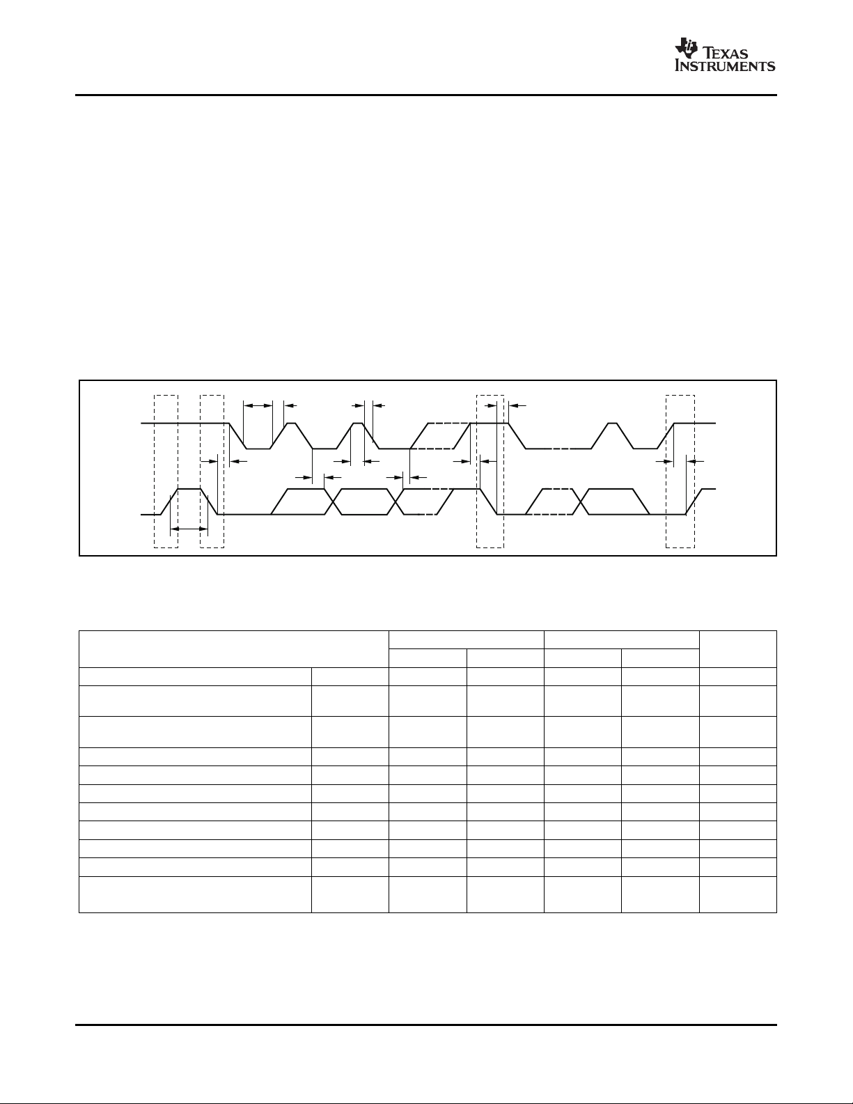
Figure 16 and Figure 17 show read and write
operation timing diagrams. Note that register bytes
are sent most-significant byte first, followed by the
least significant byte. Figure 18 shows the timing
diagram for the SMBus Alert operation. Figure 19
illustrates a typical register pointer configuration.
Submit Documentation Feedback
11
www.ti.com
Frame1Two-WireSlaveAddressByte
(1)
Frame2DataMSByte
(2)
1
StartBy
Master
ACKBy
INA209
ACKBy
Master
From
INA209
1 9 1
9
SDA
SCL
0 0 A3 R/W
D15 D14 D13 D12 D11 D10 D9 D8
A2 A1 A0
Frame3DataLSByte
(2)
StopNoACKBy
(3)
Master
From
INA209
1
9
D7 D6 D5 D4 D3 D2 D1 D0
NOTES:(1)ThevalueoftheSlaveAddressByteisdeterminedbythesettingsoftheA0andA1pins.
RefertoT
able1.
(2)Readdataisfromthelastregisterpointerlocation.Ifanewregisterisdesired,theregister
pointermustbeupdated.SeeFigure19.
(3)ACKbyMastercanalsobesent.
Frame1Two-WireSlaveAddressByte
(1)
Frame2RegisterPointerByte
StartBy
Master
ACKBy
INA209
ACKBy
INA209
1 9 1
ACKBy
INA209
1
D15 D14 D13 D12 D11 D10 D9 D8
9
9
SDA
SCL
1 0 0 A3 A2
A1 A0 R/W P7 P6 P5 P4 P3 P2 P1 P0
NOTE(1):ThevalueoftheSlaveAddressByteisdeterminedbythesettingsoftheA0andA1pins.RefertoTable1.
Frame4DataLSByteFrame3DataMSByte
ACKBy
INA209
StopBy
Master
1
D7 D6 D5 D4 D3 D2 D1 D0
9
INA209
SBOS403 – JUNE 2007
Figure 16. Timing Diagram for Write Word Format
12
Figure 17. Timing Diagram for Read Word Format
Submit Documentation Feedback
www.ti.com
Frame1SMBusALERTResponseAddressByte Frame2SlaveAddressByte
(1)
StartBy
Master
ACKBy
INA209
From
INA209
NACKBy
Master
StopBy
Master
1 9 1
9
SDA
SCL
ALERT
0 0 0 1 1 0 0 R/W
1 0 0 A3 A2 A1 A0 0
NOTE(1):ThevalueoftheSlaveAddressByteisdeterminedbythesettingsoftheA0andA1pins.RefertoTable1.
Frame1Two-WireSlaveAddressByte
(1)
Frame2RegisterPointerByte
1
StartBy
Master
ACKBy
INA209
ACKBy
INA209
1 9 1 9
SDA
SCL
0 0 A3 A2 A1 A0 R/W P7 P6 P5 P4 P3 P2 P1 P0 Stop
¼
NOTE(1):ThevalueoftheSlaveAddressByteisdeterminedbythesettingsoftheA0andA1pins.RefertoTable1.
Figure 18. Timing Diagram for SMBus ALERT
INA209
SBOS403 – JUNE 2007
Figure 19. Typical Register Pointer Set
Submit Documentation Feedback
13
www.ti.com
SCL
SDA
t
(LOW)
t
R
t
F
t
(HDSTA)
t
(HDSTA)
t
(HDDAT)
t
(BUF)
t
(SUDAT)
t
(HIGH)
t
(SUSTA)
t
(SUSTO)
P S S P
INA209
SBOS403 – JUNE 2007
High-Speed I2C Mode
When the bus is idle, both the SDA and SCL lines
are pulled high by the pull-up devices. The master
generates a start condition followed by a valid serial
byte containing High-Speed (HS) master code
00001XXX. This transmission is made in fast
(400kbps) or standard (100kbps) (F/S) mode at no
more than 400kbps. The INA209 does not
acknowledge the HS master code, but does
recognize it and switches its internal filters to support
3.4Mbps operation.
allowed. Instead of using a stop condition, repeated
start conditions should be used to secure the bus in
HS-mode. A stop condition ends the HS-mode and
switches all the internal filters of the INA209 to
support either F/S mode transmission.
The master then generates a repeated start condition
(a repeated start condition has the same timing as
the start condition). After this repeated start
condition, the protocol is the same as F/S mode,
except that transmission speeds up to 3.4Mbps are
allowed. Instead of using a stop condition, repeated
The master then generates a repeated start condition start conditions should be used to secure the bus in
(a repeated start condition has the same timing as HS-mode. A stop condition ends the HS-mode and
the start condition). After this repeated start switches all the internal filters of the INA209 to
condition, the protocol is the same as F/S mode, support the F/S mode.
except that transmission speeds up to 3.4Mbps are
PARAMETER MIN MAX MIN MAX UNITS
SCL Operating Frequency f
Bus Free Time Between STOP and START
Condition
Hold time after repeated START condition.
After this period, the first clock is generated.
Repeated START Condition Setup Time t
STOP Condition Setup Time t
Data Hold Time t
Data Setup Time t
SCL Clock LOW Period t
SCL Clock HIGH Period t
Clock/Data Fall Time t
Clock/Data Rise Time t
Clock/Data Rise Time for SCLK ≤ 100kHz t
Figure 20. Bus Timing Diagram
Bus Timing Diagram Definitions
(SCL)
t
(BUF)
t
(HDSTA)
(SUSTA)
(SUSTO)
(HDDAT)
(SUDAT)
(LOW)
(HIGH)
F
R
R
FAST MODE HIGH-SPEED MODE
0.001 0.4 0.001 3.4 MHz
600 160 ns
100 100 ns
100 100 ns
100 100 ns
0 0 ns
100 10 ns
1300 160 ns
600 60 ns
300 160 ns
300 160 ns
1000 ns
14
Submit Documentation Feedback

www.ti.com
PowerRegister
CurrentRegister
VoltageRegister
OverlimitRegister
WarningRegister
I C
Interface
2
Gnd
V
S
Supply
Voltage
V
IN-
V
IN+
Warning
Overlimit
CMP
Filter
Critical
V
I
Convert
Data
Clk
Alert
GPIO
Critical
DAC+
Critical
DAC-
Load
Supply
Current
Shunt
V =V V-
SHUNT IN+ IN-
Typically<50mV
INA209PowerSupply
3Vto5.5V
V =V GND-
BUS IN-
Rangeof0Vto26V
TypicalApplication12V
+ -
+
-
CMP
INA209
SBOS403 – JUNE 2007
Power-Up Conditions BASIC ADC FUNCTIONS
Power-up conditions apply to software reset via the The two analog inputs to the INA209, V
RST bit (bit 15) in the Configuration Register, or the connect to a shunt resistor in the bus of interest. The
I2C bus General Call Reset. At device power up, all INA209 is typically powered by a separate supply
Status bits are masked. Warning, Over-Limit, Critical, from +3V to +5.5V. The bus being sensed can vary
and SMBus Alert functions are disabled. All from 0V to 26V. There are no special considerations
watchdog outputs default to active low and for power-supply sequencing (for example, a bus
transparent (non-latched) modes. voltage can be present with the supply voltage off,
and vice-versa). The INA209 senses the small drop
across the shunt for shunt voltage, and senses the
voltage with respect to ground from V
voltage. Figure 21 illustrates this operation.
and V
IN+
for the bus
IN–
,
IN–
Figure 21. INA209 Configured for Shunt and Bus Voltage Measurement
Submit Documentation Feedback
15

www.ti.com
INA209
SBOS403 – JUNE 2007
When the INA209 is in the normal operating mode The Conversion Ready bit clears under these
(that is, MODE bits of the Configuration Register are conditions:
set to '111'), it continuously converts the shunt
voltage up to the number set in the shunt voltage
averaging function (Configuration Register, SADC
bits). The device then converts the bus voltage up to
the number set in the bus voltage averaging
(Configuration Register, BADC bits). The Mode
control in the Configuration Register also permits
selecting modes to convert only voltage or current,
either continuously or in response to an event
(triggered).
All current and power calculations are performed in
the background and do not contribute to conversion
time; conversion times shown in the Electrical
Characteristics table can be used to determine the
actual conversion time.
Power-Down mode reduces the quiescent current
and turns off current into the INA209 inputs, avoiding
any supply drain. Full recovery from Power-Down
requires 40 µ s. ADC Off mode (set by the
Configuration Register, MODE bits) stops all Shunt voltage peak registers hold the lowest and
conversions. highest converted reading for the shunt value. The
In triggered mode, the external Convert line becomes
active. Convert commands are initiated by taking the
Convert line low for a minimum of 4 µ s. The Convert
line may be connected high when unused. Any
re-trigger of the Convert line during a conversion is
ignored, and the Convert line state is disregarded
until the conversion ends. There are several
available triggered modes; however, all conversions
are performed repeatedly up to the number set in the
Averaging function (Configuration Register, BADC
and SADC bits).
If the Convert line is held low, writing any of the
triggered convert modes into the Configuration
Register (even if the desired mode is already
programmed into the register) triggers a single-shot
conversion.
Although the INA209 can be read at any time, and
the data from the last conversion remain available,
the Conversion Ready bit (Status Register, CNVR
bit) is provided to help co-ordinate one-shot or
triggered conversions. The Conversion Ready bit is
set after all conversions, averaging, and
multiplication operations are complete.
1. Writing to the Configuration Register, except
when configuring the MODE bits for Power
Down or ADC off (Disable) modes;
2. Reading the Status Register; or
3. Triggering a single-shot conversion with the
Convert pin.
Power Measurement
Current and bus voltage are converted at different
points in time, depending on the resolution and
averaging mode settings. For instance, when
configured for 12-bit and 128 sample averaging, up
to 68ms in time between sampling these two values
is possible. Again, these calculations are performed
in the background and do not add to the overall
conversion time.
Peak-Hold Registers
shunt value may be either positive or negative; as a
result, there is a need for a sign bit in either register.
For instance, the Shunt Voltage Positive Peak
Register in most systems records a positive voltage;
in most unidirectional current measurement
applications, the Shunt Voltage Negative Peak
Register also records a positive voltage. However,
certain conditions can occur in normally
unidirectional systems that cause a negative polarity
across the shunt; these events are recorded in the
Shunt Voltage Negative Peak Register.
Peak-hold registers do not record conditions that
trigger a Critical Comparator shutdown. A Critical
Comparator shutdown occurs within 5 µ s of detecting
a critical condition, while the ADC conversion
necessary to record a peak-hold requires 532 µ s.
Therefore, a system shutdown removes the fault
before the ADC can record it.
16
Submit Documentation Feedback

www.ti.com
INA209
SBOS403 – JUNE 2007
Critical Comparator PGA Function
The Critical Comparator function is included to If larger full-scale shunt voltages are desired, the
provide the fastest possible response to overload INA209 provides a PGA function that increases the
events. This function bypasses the digital circuit by full-scale range up to 2, 4, or 8 times (320mV).
capturing the event in the analog domain. Additionally, the bus voltage measurement has two
The Critical Comparator responds only to shunt
voltage, and can be programmed for a value from
0mV to 255mV (in 1mV increments) in the Critical
DAC+ and Critical DAC– Registers. Two thresholds
are provided, allowing users to set different
thresholds in systems where bi-directional current
measurement occurs. For example, a power supply
may readily allow sourcing of 10A, but must alarm
whenever sinking more than 1A. The SMBus Alert
Mask/Enable Control Register allows the user to
enable or disable the Critical pin output through the
CREN bit. The CREN bit affects only the Critical pin;
it does not affect the CRIT+ or CRIT– flags within the
Status Register.
The DAC Comparator output filter is set by the CF
bits of the Critical DAC– Register. This filter
determines the duration of time that the CMP output
must be continuously active (not toggling) to
propagate to the Critical pin output and set the
CRIT+ or CRIT– flags within the Status Register.
While the DAC Comparator output filter provides
settings from 0ms to 0.96ms, the CMP is actually
strobed every 4 µ s, providing multiple samples per
delay period. For the Critical output pin to become
active, the critical condition must be true for every
sample during the specified delay period.
When using the Critical Comparator in unidirectional
applications, where the Critical DAC– Register is
unused, the Comparator could trip in error if the input
is near zero, because the comparator can have an
offset of up to ± 1.5mV. Noise also contributes to
false tripping. To avoid false tripping in unidirectional
applications, the Critical DAC– should be
programmed to a value beyond –2mV to account for
the offset, and an additional amount to provide a
noise margin. Alternatively, the Critical DAC– can be
programmed to negative full-scale range (–255mV),
in order to eliminate false tripping.
full-scale ranges: 16V or 32V.
Compatibility with TI Hot Swap Controllers
The INA209 is designed for compatibility with hot
swap controllers such the TI TPS2490 . The
TPS2490 uses a high-side shunt with a limit at
50mV; the INA209 full-scale range of 40mV enables
the use of the same shunt for current sensing below
this limit. When sensing is required at (or through)
the 50mV sense point of the TPS2490, the PGA of
the INA209 can be set to ÷2 to provide an 80mV
full-scale range.
A typical application connects the Critical pin output
to the TPS2490 enable line; this configuration
enables user-programmable current limits. Note that
the latched mode should be used for the Critical pin
output to avoid oscillation at the trip level.
Filtering and Input Considerations
Measuring current is often noisy, and such noise can
be difficult to define. The INA209 offers several
options for filtering by choosing resolution and
averaging in the Configuration Register. These
filtering options can be set independently for either
voltage or current measurement.
The internal ADC is based on a delta-sigma ( ∆ Σ )
front-end with a 500kHz ( ± 30%) typical sampling
rate. This architecture has good inherent noise
rejection; however, transients that occur at or very
close to the sampling rate harmonics can cause
problems. Because these signals are at 1MHz and
higher, they can be dealt with by incorporating
filtering at the input of the INA209. The high
frequency enables the use of low-value series
resistors on the filter for negligible effects on
measurement accuracy. Figure 22 shows the INA209
with an additonal filter added at the input.
Submit Documentation Feedback
17

www.ti.com
PowerRegister
CurrentRegister
VoltageRegister
OverlimitRegister
WarningRegister
I C
Interface
2
Gnd
V
S
Supply
Voltage
V
IN-
V
IN+
Warning
Overlimit
CMP
Filter
Critical
V
I
Convert
Data
Clk
Alert
GPIO
Critical
DAC+
Critical
DAC-
Supply
Load
Current
Shunt
R 10W
FILTER
R 10W
FILTER
0.1 Fto1 Fm m
Ceramiccapacitor
3.3VSupply
CriticalOutput
OverlimitOutput
WarningOutput
Data(SDA)
Clock(SCL)
CMP
INA209
SBOS403 – JUNE 2007
Figure 22. INA209 with Input Filtering
Overload conditions are another consideration for the
INA209 inputs. The INA209 inputs are specified to
tolerate 26V across the inputs. A large differential
scenario might be a short to ground on the load side
of the shunt. This type of event can result in full
power-supply voltage across the shunt (as long the
power supply or energy storage capacitors support
it). It must be remembered that removing a short to
ground can result in inductive kickbacks that could
exceed the 26V differential and common-mode rating
of the INA209. Inductive kickback voltages are best
dealt with by zener-type transient-absorbing devices
(commonly called transzorbs) combined with
sufficient energy storage capacitance.
In applications that do not have large energy storage
electrolytics on one or both sides of the shunt, an
input overstress condition may result from an
excessive dV/dt of the voltage applied to the input. A
hard physical short is the most likely cause of this
event, particularly in applications with no large
electrolytics present. This problem occurs because
an excessive dV/dt can activate the ESD protection
in the INA209 in systems where large currents are
available. Testing has demonstrated that the addition
of 10 Ω resistors in series with each input of the
INA209 sufficiently protects the inputs against dV/dt
failure up to the 26V rating of the INA209. These
resistors have no significant effect on accuracy.
18
Submit Documentation Feedback
SMBus Alert Response
The ALERT interrupt pin is set whenever Warning,
Over-Limit, Critical faults, or Conversion Ready
states (in triggered modes) occur. The ALERT
interrupt output signal is latched and can be cleared
only by either reading the Status Register or by
successfully responding to an alert response
address. If the fault is still present, the ALERT pin
re-asserts. Asserting the ALERT pin does not halt
automatic conversions that are already in progress.
The ALERT output pin is open-drain, allowing
multiple devices to share a common interrupt line.
The ALERT output can be disabled via the SMBus
Alert Mask/Enable Control Register using the
SMAEN bit. When disabled, the ALERT pin goes to a
high state.
The INA209 responds to the SMBus alert response
address, an interrupt pointer return-address feature.
The SMBus alert response interrupt pointer provides
quick fault identification for simple slave devices.
When an ALERT occurs, the master can broadcast
the alert response slave address (0001 100).
Following this alert response, any slave devices that
generated interrupts identify themselves by putting
the respective addresses on the bus.

www.ti.com
Gnd
V
SVIN-VIN+
Warning
Overlimit
Critical
Convert
Data
Clk
Alert
GPIO
I C
2
Bus
INA209
Gnd
VSV
IN-VIN+
Warning
Overlimit
Critical
Convert
Data
Clk
Alert
GPIO
INA209
Gnd
VSV
IN-VIN+
Warning
Overlimit
Critical
Convert
Data
Clk
Alert
GPIO
INA209
Gnd
V
SVIN-VIN+
Warning
Overlimit
Critical
Convert
Data
Clk
Alert
GPIO
INA209
INA209
SBOS403 – JUNE 2007
The alert response can activate several different
slave devices simultaneously, similar to the I2C
General Call. If more than one slave attempts to
respond, bus arbitration rules apply; the device with
the lower address code wins. The losing device does
not generate an Acknowledge and continues to hold
the ALERT line low until the interrupt is cleared.
Successful completion of the read alert response
protocol clears the SMBus ALERT pin, provided that
the condition causing the alert no longer exists. The
SMBus Alert flag is cleared separately by either
reading the Status Register or by disabling the
SMBus Alert function.
The Status Register flags indicate which (if any) of
the watchdogs have been activated. After power-on
reset (POR), the normal state of all flag bits is '0',
assuming that no alarm conditions exist. The flags
are cleared by any successful read of the Status
Register, after a conversion is complete and the fault
no longer exists.
All Other Latches
Figure 23. Multichannel Data Acquisition with
Simultaneous Sampling
The latches in the Configuration Register for the
Warning, Over-Limit, and Critical outputs are not
associated with the SMBus alert response, and are
cleared whenever the Status Register is read. If the
fault remains, they continue to set (they may also be
cleared by setting the latch enable to transparent,
and then returning it to latch mode).
The values in the Peak-Hold Registers must be
cleared by writing a '1' to the respective LSBs.
Multichannel Data Acquisition
The INA209 can be used in multiple current
measurement channels where the controlling
processor sums the currents of all the channels for a
total current. Often these current measurements
must occur simultaneously. Use the GPIO output
from one of the INA209s and connect it to the
Convert pin of the other INA209s. This architecture
allows for sending conversion commands via the I2C
bus to the master device, and all devices will convert
simultaneously. Figure 23 illustrates this architecture
using four INA209s.
Submit Documentation Feedback
19

www.ti.com
PowerRegister
CurrentRegister
VoltageRegister
OverlimitRegister
WarningRegister
I C
Interface
2
Gnd
V
S
Supply
Voltage
V
IN-
V
IN+
Warning
Overlimit
CMP
Filter
Critical
V
I
Convert
Data
Clk
Alert
GPIO
Critical
DAC+
Shunt
ControlFET
FromHot
Swap
Controller
P-channelMOSFETs
dualpairssuchasVishay
Si3991DV
N-channelMOSFETs
dualpairsuchasVishay
Si1034
10kW 10kW
R
SHUNT
Critical
DAC-
CMP
INA209
SBOS403 – JUNE 2007
External Circuitry for Additional V
The INA209 GPIO can be used to control an external
circuit to switch the V
alternate location. Switching is most often done to
perform bus voltage measurements on the opposite
measurement to an
BUS
Input
BUS
create errors through the resistance of any external
switching method used. The easiest way to avoid
these errors is by reducing this resistance to a
minimum; select switching MOSFETs with the lowest
possible R
values.
DS(on)
side of a MOSFET switch in series with the shunt The circuit shown in Figure 24 uses MOSFET pairs
resistor. to reduce package count. Back-to-back MOSFETs
Consideration must be given to the typical 11 µ A
input current of each INA209 input, along with the
320k Ω impedance present at the V
input where
IN–
the bus voltage is measured. These effects can
must be used in each leg because of the built-in
back diodes from source-to-drain. In this circuit, the
normal connection for V
is at the shunt, with the
IN–
optional voltage measurement at the output of the
control FET.
20
Figure 24. External Circuitry for Additional V
Submit Documentation Feedback
Input
BUS

www.ti.com
MaxI=
V
R
SHUNT
SHUNT
Current_LSB=
Max_Expected_I
CurrentRegisterh
Current_LSB=
Max_Expected_I
7FFFh
Max_Expected_I
32767
=
Current_LSB=
Max_Expected_I
1FFFh
Max_Expected_I
8191
=
Current_LSB=
Max_Expected_I
FA0h
Max_Expected_I
4000d
=
Cal=trunc
0.04096
Current_LSB R
SHUNT
´
Power_LSB=Volt_LSB Current_LSB 5000=Power_LSB=20 Current_LSB´ ´ ´
INA209
SBOS403 – JUNE 2007
PROGRAMMING THE INA209 POWER MEASUREMENT ENGINE
Calibration Register and Scaling
The Calibration Register makes it possible to set the scaling of the Current and Power Registers to whatever
values are most useful for a given application. One strategy may be to set the Calibration Register such that the
largest possible number is generated in the Current Register or Power Register at the expected full-scale point;
this approach yields the highest resolution. The Calibration Register can also be selected to provide values in
the Current and Power Registers that either provide direct decimal equivalents of the values being measured, or
yield a round LSB number. After these choices have been made, the Calibration Register also offers possibilities
for end user system-level calibration, where the value is adjusted slightly to cancel total system error.
Follow these steps to select a proper value for the the Calibration Register.
1. Establish the following parameters (for a given application):
– Maximum bus voltage, V
– Shunt resistance, R
– Desired maximum drop across the shunt, V
2. Determine maximum possible current using Equation 1 :
3. Choose the desired maximum current value: Max_Expected_I, ≤ MaxI
4. Calculate the possible range of current LSBs. The general form of this calculation is given by Equation 2 :
BUS
SHUNT
( ≥ 40mV recommended)
SHUNT
(1)
where CurrentRegister represents the value in the INA209 Current Register.
There are several ways to determine an appropriate Current Register value. One method is to fill the
Current Register to the largest possible value at Max_Expected_I for highest accuracy and resolution, as
shown in Equation 3 .
A second method uses a selected LSB based on a required 12-bit resolution, as illustrated by Equation 4 :
A third possible way to determine a proper Current Register value is to choose a decimal value for the
register that corresponds to the known current. For example, Equation 5 uses 4000d to representa 4A or
40A current:
A final option is to simply use a current LSB of your own choice. The selected value must be less than
that specified by Equation 2 .
5. Compute the Calibration Register value using Equation 6 :
6. Calculate the Power LSB, using Equation 7 . Equation 7 shows a general formula; because the bus
voltage measurement LSB is always 4mV, the general formula reduces to the calculated result.
(2)
(3)
(4)
(5)
(6)
(7)
Submit Documentation Feedback
21

www.ti.com
Max_Current=Current_LSB 7FFFh=Current_LSB 32767´ ´
Max_ShuntVoltage=Max_Current R´
SHUNT
MaxI=
V
R
SHUNT
SHUNT
= =4A
0.04
0.01
Current_LSB=
Max_Expected_I
7FFFh
Max_Expected_I
32767
2
32767
= = =61.037 A
-
6
Current_LSB=
Max_Expected_I
1FFFh
Max_Expected_I
8191
2
8191
= = =244.17 A
-
6
Cal=trunc
0.04096
Current_LSB R
SHUNT
´
0.04096
=trunc =20480d=5000h
100 0.01
-6
´
Power_LSB=Volt_LSB Current_LSB 5000=Power_LSB=20 Current_LSB=2 A
-3
´ ´ ´
Max_Current=Current_LSB 7FFFh=Current_LSB 32767=2 32767=3.2767A
-3
´ ´ ´
Max_ShuntVoltage=Max_Current R
SHUNT
´ =3.2767 0.01=32.767
-3
´
INA209
SBOS403 – JUNE 2007
7. Compute the maximum current and shunt voltage values (before overflow), as shown by Equation 8 and
Equation 9 :
Typical Design Example
This section presents a typical design example for the INA209 using the process described in the previous
section . For this example, we will use a nominal 12V system.
1. Establish the following parameters:
– Maximum bus voltage: V
– Shunt resistance: R
SHUNT
– Desired maximum drop across the shunt, V
INA209 for a 40mV full-scale range)
2. Determine maximum possible current using Equation 10 :
3. Choose the desired maximum current value: Max_Expected_I, ≤ MaxI. For this example, we will use 2A.
4. Calculate the possible range of current LSBs. The general form of this calculation is given by Equation 2 .
In this example, we will calculate a Current Register value using three of the four possible methods.
First, use Equation 11 to fill the Current Register to the largest possible value at Max_Expected_I for
highest accuracy and resolution:
BUS
= 0.01 Ω
= 16V
= 40mV (based on the option of programming the
SHUNT
(8)
(9)
(10)
The second method, using Equation 12 , generates a selected LSB based on a required 12-bit resolution:
The third option uses a current LSB that must be less than that specified by Equation 2 ; in this instance,
we choose to set the current LSB equal to:
–6
100
A
This option provides a straighforward LSB that eases our remaining calculations. This value is also within
the range of the other two results given by Equation 11 and Equation 12 .
5. Now we compute the Calibration Register value according to Equation 13 :
6. Then we calculate the Power LSB, using Equation 14 :
7. Finally, we compute the maximum current and shunt voltage values (before overflow), as shown by
Equation 15 and Equation 16 :
(11)
(12)
(13)
(14)
(15)
(16)
22
Submit Documentation Feedback

www.ti.com
INA209
SBOS403 – JUNE 2007
REGISTER INFORMATION
The INA209 uses a bank of registers for holding Register contents are updated 4 µ s after completion
configuration settings, measurement results, of the write command. Therefore, a 4 µ s delay is
maximum/minimum limits, and status information. required between completion of a write to a given
Table 2 summarizes the INA209 registers; Figure 14 register and a subsequent read of that register
illustrates them. (without changing the pointer) when using SCL
frequencies in excess of 1MHz.
Table 2. Summary of Register Set
POINTER
ADDRESS POWER-ON RESET
HEX REGISTER NAME FUNCTION BINARY HEX TYPE
00 Configuration Register voltage range, PGA Gain, ADC 00111001 10011111 399F R/ W
01 Status Register over-/under-limits, conversion ready, 00000000 00000000 0000 R
02 00000000 00000000 0000 R/ W
03 Shunt Voltage Shunt voltage measurement data. 00000000 00000000 0000 R
04 Bus Voltage Bus voltage measurement data. 00000000 00000000 0000 R
05 Power Power measurement data. 00000000 00000000 0000 R
06 Current/PGA
07 10000000 00000000 8000 R/ W
08 01111111 11111111 7FFF R/ W
09 00000000 00000000 0000 R/ W
0A 11111111 11111000 FFF8 R/ W
0B Power Peak 00000000 00000000 0000 R/ W
0C 00000000 00000000 0000 R/ W
0D 00000000 00000000 0000 R/ W
0E Power Warning 00000000 00000000 0000 R/ W
0F flag in the Status Register, and activates 00000000 00000000 0000 R/ W
(1) Type: R = Read-Only, R/ W = Read/Write.
(2) Current Register defaults to '0' because the Calibration Register defaults to '0', yielding a zero current value until the Calibration Register
is programmed.
SMBus Alert Mask/Enable Enables/disables flags in the Status
Control Register Register
(2)
Shunt Voltage Positive Contains most positive voltage reading
Peak of Shunt Voltage Register.
Shunt Voltage Negative Contains most negative voltage reading
Peak of Shunt Voltage Register.
Bus Voltage Maximum Contains highest voltage reading of Bus
Peak Voltage Register.
Bus Voltage Minimum Contains lowest voltage reading of Bus
Peak Voltage Register.
Shunt Voltage Positive positive shunt voltage limit that triggers
Warning a warning flag in the Status Register,
Shunt Voltage Negative negative shunt voltage limit that triggers
Warning a warning flag in the Status Register,
Bus Over-Voltage
Warning
All-register reset, settings for bus
resolution/averaging.
Status flags for warnings,
math overflow, and SMBus Alert.
Contains the value of the current flowing
through the shunt resistor.
Contains highest power reading of
Power Register.
Warning watchdog register. Sets
and activates Warning pin.
Warning watchdog register. Sets
and activates Warning pin.
Warning watchdog register. Sets power
limit that triggers a warning flag in the
Status Register, and activates Warning
pin.
Warning watchdog register. Sets high
Bus voltage limit that triggers a warning
Warning pin. Also contains bits to set
Warning pin polarity and latch feature.
00000000 00000000 0000 R
(1)
Submit Documentation Feedback
23

www.ti.com
INA209
SBOS403 – JUNE 2007
Table 2. Summary of Register Set (continued)
POINTER
ADDRESS POWER-ON RESET
HEX REGISTER NAME FUNCTION BINARY HEX TYPE
10 00000000 00000000 0000 R/ W
11 Power Over-Limit 00000000 00000000 0000 R/ W
12 00000000 00000000 0000 R/ W
13 00000000 00000000 0000 R/ W
14 (Critical Shunt Positive and mode of operation, Critical 00000000 00000000 0000 R/ W
15 (Critical Shunt Negative 00000000 00000000 0000 R/ W
16 Calibration and power measurements. Overall 00000000 00000000 0000 R/ W
Bus Under-Voltage Bus voltage limit that triggers a warning
Warning flag in the Status Register and activates
Bus Over-Voltage over-limit flag in the Status Register,
Over-Limit and activates the Overlimit pin. Also
Bus Under-Voltage under-voltage limit that triggers an
Over-Limit over-limit flag in the Status Register,
Critical DAC+ Register DAC+. Contains bits for GPIO pin status
Voltage) Comparator latch feature and
Critical DAC– Register
Voltage)
Warning watchdog register. Sets low
Warning pin.
Over-limit watchdog register. Sets
power limit that triggers an over-limit
flag in the Status Register, and activates
the Overlimit pin.
Over-limit watchdog register. Sets Bus
over-voltage limit that triggers an
contains bits to set Overlimit pin polarity
and latch feature.
Over-limit watchdog register. Sets Bus
and activates the Overlimit pin.
Sets a positive limit for internal Critical
hysteresis.
Sets a negative limit for internal Critical
DAC+. Contains bits for Warning pin
delay, and Critical Comparator output
filter configuration.
Sets full-scale range and LSB of current
system calibration.
(1)
24
Submit Documentation Feedback

www.ti.com
SBOS403 – JUNE 2007
REGISTER DETAILS
All INA209 registers are 16-bit registers. 16-bit register data are sent in two 8-bit bytes via the I2C interface.
Configuration Register 00h (Read/Write)
BIT # D15 D14 D13 D12 D11 D10 D9 D8 D7 D6 D5 D4 D3 D2 D1 D0
BIT
NAME
POR
VALUE
RST: Reset Bit
Bit 15 Setting this bit to 1 generates a system reset that is the same as power-on reset. Resets all
BRNG: Bus Voltage Range
Bit 13 0 = 16V FSR
PG: PGA (Shunt Voltage Only)
Bits 11, 12 Sets PGA gain and range. Note that the PGA defaults to ÷ 8 (320mV range). Table 3 shows
RST — BRNG PG1 PG0 BADC4 BADC3 BADC2 BADC1 SADC4 SADC3 SADC2 SADC1 MODE3 MODE2 MODE1
0 0 1 1 1 0 0 1 1 0 0 1 1 1 1 1
Bit Descriptions
registers to default values, this bit self-clears.
1 = 32V FSR (default value)
the gain and range for the various PG settings.
INA209
Table 3. PG Bit Settings
PG1 PG0 GAIN RANGE
0 0 1 ± 40mV
0 1 ÷ 2 ± 80mV
1 0 ÷ 4 ± 160mV
1 1 ÷ 8 ± 320mV
(1) Shaded values are default.
(1)
BADC: BADC Bus ADC Resolution/Averaging
Bits 7–10 These bits adjust the Bus ADC resolution (9-, 10-, 11-, or 12-bit) or set the number of
samples used when averaging results for the Bus Voltage Register (04h).
Submit Documentation Feedback
25
www.ti.com
INA209
SBOS403 – JUNE 2007
SADC: SADC Shunt ADC Resolution/Averaging
Bits 3–6 These bits adjust the Shunt ADC resolution (9-, 10-, 11-, or 12-bit) or set the number of
samples used when averaging results for the Shunt Voltage Register (03h).
BADC (Bus) and SADC (Shunt) ADC resolution/averaging and conversion time settings are
shown in Table 4 .
Table 4. ADC Settings
ADC4 ADC3 ADC2 ADC1 MODE/SAMPLES CONVERSION TIME
0 X
0 X
0 X
0 X
1 0 0 0 12-bit 532 µ s
1 0 0 1 2 1.06ms
1 0 1 0 4 2.13ms
1 0 1 1 8 4.26ms
1 1 0 0 16 8.51ms
1 1 0 1 32 17.02ms
1 1 1 0 64 34.05ms
1 1 1 1 128 68.10ms
(1) Shaded values are default.
(2) X = Don't care.
(2)
(2)
(2)
(2)
0 0 9-bit 84 µ s
0 1 10-bit 148 µ s
1 0 11-bit 276 µ s
1 1 12-bit 532 µ s
(1)
MODE: Operating Mode
Bits 0–2 Selects continuous, triggered, or power-down mode of operation. These bits default to
continuous shunt and bus measurement mode. The mode settings are shown in Table 5 .
Table 5. Mode Settings
MODE3 MODE2 MODE1 MODE
0 0 0 Power-Down
0 0 1 Shunt Voltage, Triggered
0 1 0 Bus Voltage, Triggered
0 1 1 Shunt and Bus, Triggered
1 0 0 ADC Off (disabled)
1 0 1 Shunt Voltage, Continuous
1 1 0 Bus Voltage, Continuous
1 1 1 Shunt and Bus, Continuous
(1) Shaded values are default.
(1)
26
Submit Documentation Feedback

www.ti.com
INA209
SBOS403 – JUNE 2007
Status Register 01h (Read)
BIT # D15 D14 D13 D12 D11 D10 D9 D8 D7 D6 D5 D4 D3 D2 D1 D0
BIT
NAME
POR
VALUE
The Status Register flags activate whenever any limit is violated, and latch when corresponding latch bits are
set. These flags are cleared when the Status Register is read (unless a limit is exceeded when the flag
immediately sets again).
After power-up and initial setup, the Status Register should be read once to clear any flags set as as a result of
power-up values prior to setup.
WOV: Warning Bus Over-Voltage
Bit 15 This bit is set to '1' when the result in the Bus Voltage Register (04h) exceeds the level set
WUV: Warning Bus Under-Voltage
Bit 14 This bit is set to '1' when the result in the Bus Voltage Register (04h) is less than the value
WP: Warning Power
Bit 13 This bit is set to '1' when the value of the Power Register (05h) exceeds the level set in the
WS+: Warning Shunt+ Voltage
Bit 12 This bit is set to '1' when the value of the Shunt Voltage Register (03h) exceeds the level
WS–: Warning Shunt– Voltage
Bit 11 This bit is set to '1' when the value of the Shunt Voltage Register (03h) exceeds the level
OLOV: Over-Limit Bus Over-Voltage
Bit 10 This bit is set to '1' when the result in the Bus Voltage Register (04h) exceeds the level set
OLUV: Over-Limit Bus Under-Voltage
Bit 9 This bit is set to '1' when the result in the Bus Voltage Register (04h) is less than the level
OLP: Over-Limit Power
Bit 8 This bit is set to '1' when the value of the Power Register (05h) exceeds the level set in the
WOV WUV WP WS+ WS– OLOV OLUV OLP CRIT+ CRIT– CNVR SMBA OVF — — —
0 0 0 0 0 0 0 0 0 0 0 0 0 0 0 0
Bit Descriptions
in the Bus Over-Voltage Warning Register (0Fh).
set in the Bus Under-Voltage Warning Register (10h).
Power Warning Register (0Eh).
set in the Shunt Voltage Positive Warning Register (0Ch).
set in the Shunt Voltage Negative Warning Register (0Dh).
in the Bus Over-Voltage Over-Limit Register (12h).
set in the Bus Under-Voltage Over-Limit Register (13h).
Power Over-Limit Register (11h).
Submit Documentation Feedback
27

www.ti.com
INA209
SBOS403 – JUNE 2007
Bit Descriptions (continued)
CRIT+: Critical Shunt Positive Voltage
Bit 7 This bit is set to '1' when the value of the shunt voltage exceeds the positive limit set in the
Critical DAC+ Register (14h).
CRIT–: Critical Shunt Negative Voltage
Bit 6 This bit is set to '1' when the value of the shunt voltage exceeds the negative limit set in the
Critical DAC– Register (15h).
CNVR: Conversion Ready
Bit 5 Although the INA209 can be read at any time, and the data from the last conversion are
available, the Conversion Ready line is provided to help coordinate one-shot or triggered
conversions. The Conversion bit is set after all conversions, averaging, and multiplications
are complete. Conversion Ready clears under the following conditions:
1. Writing the Configuration Register (except for Power-Down or Disable mode
selections).
2. Reading the Status Register.
3. Trigger a single-shot conversion with the Convert pin.
SMBA: SMBus Alert
Bit 4 Clears only on reading Status Register or by disabling SMBus Alert function.
OVF: Math Overflow
Bit 3 This bit is set to '1' if an arithmetic operation resulted in an overflow error. It indicates that
current and power data may be meaningless. It does not set any watchdog outputs.
28
Submit Documentation Feedback

www.ti.com
INA209
SBOS403 – JUNE 2007
SMBus Alert Mask/Enable Control Register 02h (Read/Write)
BIT # D15 D14 D13 D12 D11 D10 D9 D8 D7 D6 D5 D4 D3 D2 D1 D0
BIT
NAME
POR
VALUE
Bits D5–D15 of the SMBus Alert Mask Register mask correspond to bits D5 to D15 of the Status Register to
prevent them from initiating an SMBus Alert. It does not prevent the Status Register bit from setting. Writing a '0'
to an SMBus Alert Mask bit masks it from activating the SMBus Alert. All default values are '0'.
MWOV: Warning Bus Over-Voltage Mask
Bit 15 When set to '0', this bit masks the WOV bit of the Status Register.
MWUV: Warning Bus Under-Voltage Mask
Bit 14 When set to '0', this bit masks the WUV bit of the Status Register.
MWP: Warning Power Mask
Bit 13 When set to '0', this bit masks the WP bit of the Status Register.
MWS+: Warning Shunt Positive Voltage Mask
Bit 12 When set to '0', this bit masks the WS+ bit of the Status Register.
MWS–: Warning Shunt Negative Voltage Mask
Bit 11 When set to '0', this bit masks the WS– bit of the Status Register.
MOLOV: Over-Limit Bus Over-Voltage Mask
Bit 10 When set to '0', this bit masks the OLOV bit of the Status Register.
MOLUV: Over-Limit Bus Under-Voltage Mask
Bit 9 When set to '0', this bit masks the OLUV bit of the Status Register.
MOLP: Over-Limit Power Mask
Bit 8 When set to '0', this bit masks the OLP bit of the Status Register.
MCRIT+: Critical Shunt Positive Voltage Mask
Bit 7 When set to '0', this bit masks the CRIT+ bit of the Status Register.
MCRIT–: Critical Shunt Negative Voltage Mask
Bit 6 When set to '0', this bit masks the CRIT– bit of the Status Register.
MCNVR: Conversion Ready Mask
Bit 5 When set to '0', this bit masks the CNVR bit of the Status Register.
SMAEN: SMBus Alert Enable
Bit 3 1 = Enable SMBus Alert
CREN: Critical DAC Enable
Bit 2 Enables/disables operation of the Critical pin output.
OLEN: Over-Limit Enable
Bit 1 Enables/disables operation of the Overlimit pin output.
MWOV MWUV MWP MWS+ MWS– MOLOV MOLUV MOLP MCRIT+ MCRIT– MCNVR — SMAEN CREN OLEN WRNEN
0 0 0 0 0 0 0 0 0 0 0 0 0 0 0 0
Bit Descriptions
0 = Disable SMBus Alert (default)
1 = Enabled
0 = Disabled (default)
1 = Enabled
0 = Disabled (default)
Submit Documentation Feedback
29

www.ti.com
INA209
SBOS403 – JUNE 2007
Bit Descriptions (continued)
WRNEN: Warning Enable
Bit 0 Enables/disables operation of the Warning pin output.
1 = Enabled
0 = Disabled (default)
DATA OUTPUT REGISTERS
Shunt Voltage Register 03h (Read-Only)
The Shunt Voltage Register stores the current shunt voltage reading, V
shifted according to the PGA setting selected in the Configuration Register (00h). When multiple sign bits are
present, they will all be the same value. Negative numbers are represented in two's complement format.
Generate the two's complement of a negative number by complementing the absolute value binary number and
adding 1. Extend the sign, denoting a negative number by setting the MSB = '1'. Extend the sign to any
additional sign bits to form the 16-bit word.
At PGA = ÷ 8, full-scale range = ± 320mV (decimal = 32000, positive value hex = 7D00, negative value hex =
8300), and LSB = 10 µ V.
BIT # D15 D14 D13 D12 D11 D10 D9 D8 D7 D6 D5 D4 D3 D2 D1 D0
BIT
NAME
POR
VALUE
SIGN SD14_8 SD13_8 SD12_8 SD11_8 SD10_8 SD9_8 SD8_8 SD7_8 SD6_8 SD5_8 SD4_8 SD3_8 SD2_8 SD1_8 SD0_8
0 0 0 0 0 0 0 0 0 0 0 0 0 0 0 0
. Shunt Voltage Register bits are
SHUNT
At PGA = ÷ 4, full-scale range = ± 160mV (decimal = 16000, positive value hex = 3E80, negative value hex =
C180), and LSB = 10 µ V.
BIT # D15 D14 D13 D12 D11 D10 D9 D8 D7 D6 D5 D4 D3 D2 D1 D0
BIT
NAME
POR
VALUE
SIGN SIGN SD13_4 SD12_4 SD11_4 SD10_4 SD9_4 SD8_4 SD7_4 SD6_4 SD5_4 SD4_4 SD3_4 SD3_4 SD1_4 SD0_4
0 0 0 0 0 0 0 0 0 0 0 0 0 0 0 0
At PGA = ÷ 2, full-scale range = ± 80mV (decimal = 8000, positive value hex = 1F40, negative value hex =
E0C0), and LSB = 10 µ V.
BIT # D15 D14 D13 D12 D11 D10 D9 D8 D7 D6 D5 D4 D3 D2 D1 D0
BIT
NAME
POR
VALUE
SIGN SIGN SIGN SD12_2 SD11_2 SD10_2 SD9_2 SD8_2 SD7_2 SD6_2 SD5_2 SD4_2 SD3_2 SD2_2 SD1_2 SD0_2
0 0 0 0 0 0 0 0 0 0 0 0 0 0 0 0
At PGA = ÷ 1, full-scale range = ± 40mV (decimal = 4000, positive value hex = 0FA0, negative value hex = F060),
and LSB = 10 µ V.
BIT # D15 D14 D13 D12 D11 D10 D9 D8 D7 D6 D5 D4 D3 D2 D1 D0
BIT
NAME
POR
VALUE
SIGN SIGN SIGN SIGN SD11_1 SD10_1 SD9_1 SD8_1 SD7_1 SD6_1 SD5_1 SD4_1 SD3_1 SD2_1 SD1_1 SD0_1
0 0 0 0 0 0 0 0 0 0 0 0 0 0 0 0
30
Submit Documentation Feedback

www.ti.com
Power=
Current BusVoltage´
5000
Current=
ShuntVoltage CALIBRATION´
4096
SBOS403 – JUNE 2007
Bus Voltage Register 04h (Read-Only)
The Bus Voltage Register stores the most recent bus voltage reading, V
.
BUS
At full-scale range = 32V (decimal = 8000, hex = 1F40), and LSB = 4mV.
BIT # D15 D14 D13 D12 D11 D10 D9 D8 D7 D6 D5 D4 D3 D2 D1 D0
BIT
NAME
POR
VALUE
BD12 BD11 BD10 BD9 BD8 BD7 BD6 BD5 BD4 BD3 BD2 BD1 BD0 — — —
0 0 0 0 0 0 0 0 0 0 0 0 0 0 0 0
At full-scale range = 16V (decimal = 4000, hex = 0FA0), and LSB = 4mV.
BIT # D15 D14 D13 D12 D11 D10 D9 D8 D7 D6 D5 D4 D3 D2 D1 D0
BIT
NAME
POR
VALUE
0 BD11 BD10 BD9 BD8 BD7 BD6 BD5 BD4 BD3 BD2 BD1 BD0 — — —
0 0 0 0 0 0 0 0 0 0 0 0 0 0 0 0
Power Register 05h (Read-Only)
Full-scale range and LSB are set by the Calibration Register. See the Programming the INA209 Power
Measurement Engine section.
BIT # D15 D14 D13 D12 D11 D10 D9 D8 D7 D6 D5 D4 D3 D2 D1 D0
BIT
NAME
POR
VALUE
PD15 PD14 PD13 PD12 PD11 PD10 PD9 PD8 PD7 PD6 PD5 PD4 PD3 PD2 PD1 PD0
0 0 0 0 0 0 0 0 0 0 0 0 0 0 0 0
INA209
The Power Register records power in watts by multiplying the values of the current with the value of the bus
voltage according to the equation:
Current/PGA Register 06h (Read-Only)
Full-scale range and LSB depend on the value entered in the Calibration Register. See the Programming the
INA209 Power Measurement Engine section. Negative values are stored in two's complement format.
BIT # D15 D14 D13 D12 D11 D10 D9 D8 D7 D6 D5 D4 D3 D2 D1 D0
BIT
NAME
POR
VALUE
CSIGN CD14 CD13 CD12 CD11 CD10 CD9 CD8 CD7 CD6 CD5 CD4 CD3 CD2 CD1 CD0
0 0 0 0 0 0 0 0 0 0 0 0 0 0 0 0
The value of the Current Register is calculated by multiplying the value in the Short Voltage Register with the
value in the Calibration Register according to the equation:
Submit Documentation Feedback
31

www.ti.com
INA209
SBOS403 – JUNE 2007
PEAK-HOLD REGISTERS
Note: All peak-hold registers are cleared and reset to POR values by writing a '1' into the respective D0 bits.
Shunt Voltage Positive Peak Register 07h (Read/Write)
Mirrors highest voltage reading of the Shunt Voltage Register (03h).
BIT # D15 D14 D13 D12 D11 D10 D9 D8 D7 D6 D5 D4 D3 D2 D1 D0
BIT SPP SPP0/R
NAME SIGN S
POR
VALUE
Shunt Voltage Negative Peak Register 08h (Read/Write)
Mirrors lowest voltage reading (positive or negative) of the Shunt Voltage Register (03h).
BIT # D15 D14 D13 D12 D11 D10 D9 D8 D7 D6 D5 D4 D3 D2 D1 D0
BIT SPN SPN0/R
NAME SIGN S
POR
VALUE
Bus Voltage Maximum Peak Register 09h (Read/Write)
Mirrors highest voltage reading of the Bus Voltage Register (04h).
BIT # D15 D14 D13 D12 D11 D10 D9 D8 D7 D6 D5 D4 D3 D2 D1 D0
BIT
NAME
POR
VALUE
SPP14 SPP13 SPP12 SPP11 SPP10 SPP9 SPP8 SPP7 SPP6 SPP5 SPP4 SPP3 SPP2 SPP1
1 0 0 0 0 0 0 0 0 0 0 0 0 0 0 0
SPN14 SPN13 SPN12 SPN11 SPN10 SPN9 SPN8 SPN7 SPN6 SPN5 SPN4 SPN3 SPN2 SPN1
0 1 1 1 1 1 1 1 1 1 1 1 1 1 1 1
BH12 BH11 BH10 BH9 BH8 BH7 BH6 BH5 BH4 BH3 BH2 BH1 BH0 — — BPK/RS
0 0 0 0 0 0 0 0 0 0 0 0 0 0 0 0
Bus Voltage Minimum Peak Register 0Ah (Read/Write)
Mirrors lowest voltage reading of the Bus Voltage Register (04h).
BIT # D15 D14 D13 D12 D11 D10 D9 D8 D7 D6 D5 D4 D3 D2 D1 D0
BIT
NAME
POR
VALUE
BL12 BL11 BL10 BL9 BL8 BL7 BL6 BL5 BL4 BL3 BL2 BL1 BL0 — — BL/RS
1 1 1 1 1 1 1 1 1 1 1 1 1 0 0 0
Power Peak Register 0Bh (Read/Write)
Mirrors highest reading of the Power Register (05h).
BIT # D15 D14 D13 D12 D11 D10 D9 D8 D7 D6 D5 D4 D3 D2 D1 D0
BIT PPK0/R
NAME S
POR
VALUE
PPK15 PPK14 PPK13 PPK12 PPK11 PPK10 PPK9 PPK8 PPK7 PPK6 PPK5 PPK4 PPK3 PPK2 PPK1
0 0 0 0 0 0 0 0 0 0 0 0 0 0 0 0
32
Submit Documentation Feedback

www.ti.com
SBOS403 – JUNE 2007
WARNING WATCHDOG REGISTERS
These registers set warning limits that trigger flags in the Status Register and activate the Warning pin. Note:
Delayed output is set in the Critical DAC– Register (15h).
Shunt Voltage Positive Warning Register 0Ch (Read/Write)
At full-scale range = ± 320mV, 15-bit + sign, LSB = 10 µ V (decimal = 32000, positive value hex = 7D00, negative
value hex = 8300).
BIT # D15 D14 D13 D12 D11 D10 D9 D8 D7 D6 D5 D4 D3 D2 D1 D0
BIT SWP
NAME SIGN
POR
VALUE
SWP: Sets the shunt voltage positive warning limit.
Bits 15–0 If the value of the Shunt Voltage Register (03h) exceeds this limit, the WS+ bit of the Status
Shunt Voltage Negative Warning Register 0Dh (Read/Write)
At full-scale range = 320mV (decimal = 32000, positive value hex = 7D00, negative value hex = 8300), and LSB
15 bit + sign = 10 µ V.
BIT # D15 D14 D13 D12 D11 D10 D9 D8 D7 D6 D5 D4 D3 D2 D1 D0
BIT SWN
NAME SIGN
POR
VALUE
SWP14 SWP13 SWP12 SWP11 SWP10 SWP9 SWP8 SWP7 SWP6 SWP5 SWP4 SWP3 SWP SWP1 SWP0
0 0 0 0 0 0 0 0 0 0 0 0 0 0 0 0
Bit Descriptions
Register (01h) is set to '1' and the Warning pin asserts if the WRNEN bit is set.
SWN14 SWN13 SWN12 SWN11 SWN10 SWN9 SWN8 SWN7 SWN6 SWN5 SWN4 SWN3 SWN2 SWN1 SWN0
0 0 0 0 0 0 0 0 0 0 0 0 0 0 0 0
INA209
Bit Descriptions
SWN: Sets the shunt voltage negative warning limit.
Bits 15–0 If the value of the Shunt Voltage Register (03h) is below this limit, the WS– bit of the Status
Register (01h) is set to '1' and the Warning pin asserts if the WRNEN bit is set.
Power Warning Register 0Eh (Read/Write)
At full-scale range, same as the Power Register.
BIT # D15 D14 D13 D12 D11 D10 D9 D8 D7 D6 D5 D4 D3 D2 D1 D0
BIT
NAME
POR
VALUE
PW15 PW14 PW13 PW12 PW11 PW10 PW9 PW8 PW7 PW6 PW5 PW4 PW3 PW2 PW1 PW0
0 0 0 0 0 0 0 0 0 0 0 0 0 0 0 0
Bit Descriptions
PW: Sets the power warning limit.
Bits 15–0 If the value of the Power Register (05h) exceeds this limit, the WP bit of the Status Register
(01h) is set to '1' and the Warning pin asserts if the WRNEN bit is set.
Bus Over-Voltage Warning Register 0Fh (Read/Write)
BIT # D15 D14 D13 D12 D11 D10 D9 D8 D7 D6 D5 D4 D3 D2 D1 D0
BIT
NAME
POR
VALUE
BWO12 BWO11 BWO10 BWO9 BWO8 BWO7 BWO6 BWO5 BWO4 BWO3 BWO2 BWO1 BWO0 — WPL WNL
0 0 0 0 0 0 0 0 0 0 0 0 0 0 0 0
Submit Documentation Feedback
33

www.ti.com
INA209
SBOS403 – JUNE 2007
Bit Descriptions
BWO: Sets the bus over-voltage warning limit.
Bits 15–3 If a Bus Voltage Register (04h) value exceeds this limit, the WOV bit of the Status Register
(01h) is set to '1' and the Warning pin asserts if the WRNEN bit is set.
WPL: The Warning Polarity bit sets the Warning pin polarity.
Bit 1 1 = Inverted (active-high open collector)
0 = Normal (active-low open collector) (default)
WNL: The Warning Latch bit configures the latching feature of the Warning pin.
Bit 0 1 = Latch enabled
0 = Transparent (default)
Bus Under-Voltage Warning Register 10h (Read/Write)
BIT # D15 D14 D13 D12 D11 D10 D9 D8 D7 D6 D5 D4 D3 D2 D1 D0
BIT
NAME
POR
VALUE
BWU12 BWU11 BWU10 BWU9 BWU8 BWU7 BWU6 BWU5 BWU4 BWU3 BWU2 BWU1 BWU0 — — —
0 0 0 0 0 0 0 0 0 0 0 0 0 0 0 0
Bit Descriptions
BWU: Sets the bus over-voltage warning limit.
Bits 15–3 If a Bus Voltage Register (04h) value is below this limit, the WUV bit of the Status Register
(01h) is set to '1' and the Warning pin asserts if the WRNEN bit is set.
34
Submit Documentation Feedback

www.ti.com
SBOS403 – JUNE 2007
OVER-LIMIT/CRITICAL WATCHDOG REGISTERS
These registers set the over-limit and critical DAC limits that trigger flags to be set in the Status Register and
activate the Overlimit pin or the Critical pin.
Power Over-Limit Register 11h (Read/Write)
BIT # D15 D14 D13 D12 D11 D10 D9 D8 D7 D6 D5 D4 D3 D2 D1 D0
BIT
NAME
POR
VALUE
PO: Sets the power over-limit value.
Bits 15–0 If the value of the Power Register (05h) exceeds this limit, the OLP bit of the Status
Bus Over-Voltage Over-Limit Register 12h (Read/Write)
BIT # D15 D14 D13 D12 D11 D10 D9 D8 D7 D6 D5 D4 D3 D2 D1 D0
BIT
NAME
POR
VALUE
PO15 PO14 PO13 PO12 PO11 PO10 PO9 PO8 PO7 PO6 PO5 PO4 v3 PO2 PO1 PO0
0 0 0 0 0 0 0 0 0 0 0 0 0 0 0 0
Bit Descriptions
Register (01h) is set to '1' and the Overlimit pin asserts if the OLEN bit is set.
BOO12 BOO11 BOO10 BOO9 BOO8 BOO7 BOO6 BOO5 BOO4 BOO3 BOO2 BOO1 BOO0 — OLP OLL
0 0 0 0 0 0 0 0 0 0 0 0 0 0 0 0
INA209
Bit Descriptions
BOO: Sets the bus over-voltage over-limit value.
Bits 15–3 If a Bus Voltage Register (04h) value exceeds this limit, the OLOV bit of the Status Register
(01h) is set to '1' and the Overlimit pin asserts if the OLEN bit is set.
OLP: The Over-Limit Polarity bit sets the Overlimit pin polarity.
Bit 1 1 = Inverted (asserts high)
0 = Normal (asserts low) (default)
OLL: The Over-Limit Latch bit configures the latching feature of the Overlimit pin.
Bit 0 1 = Latch enabled
0 = Transparent (default)
Bus Under-Voltage Over-Limit Register 13h (Read/Write)
BIT # D15 D14 D13 D12 D11 D10 D9 D8 D7 D6 D5 D4 D3 D2 D1 D0
BIT
NAME
POR
VALUE
BUO12 BUO11 BUO10 BUO9 BUO8 BUO7 BUO6 BUO5 BUO4 BUO3 BUO2 BUO1 BUO0 — — —
0 0 0 0 0 0 0 0 0 0 0 0 0 0 0 0
Bit Descriptions
BUO: Sets the bus under-voltage over-limit value.
Bits 15–3 If a Bus Voltage Register (04h) value is below this limit, the OLUV bit of the Status Register
(01h) is set to '1' and the Overlimit pin asserts if the OLEN bit is set.
Submit Documentation Feedback
35

www.ti.com
INA209
SBOS403 – JUNE 2007
Critical DAC+ Register (Critical Shunt Positive Voltage) 14h (Read/Write)
No sign bit (sets a positive limit only). At full-scale range = 255mV; LSB = 1mV; 8-bit.
BIT # D15 D14 D13 D12 D11 D10 D9 D8 D7 D6 D5 D4 D3 D2 D1 D0
BIT CHYST CHYST CHYST
NAME 2 1 0
POR
VALUE
(1) POR value reflects the state of the GPIO pin.
CDP: Critical DAC+ limit setting.
Bits 15–8
GP: GPIO read back.
Bit 7 Shows state of the GPIO pin.
GPM: GPIO mode bit.
Bits 6, 5 The GPIO mode settings are shown in Table 6 .
CDP7 CDP6 CDP5 CDP4 CDP3 CDP2 CDP1 CDP0 GP GMP1 GPM0 CP CRL
0 0 0 0 0 0 0 0 x
(1)
0 0 0 0 1 1 0
Bit Descriptions
Table 6. GPIO Mode Settings
GPM1 GPM0 STATE NOTES
0 0 Hi-Z
0 1 Hi-Z
1 0 0
1 1 1
(1) Shaded values are default.
CP: Configures the Critical output pin polarity (open-drain output).
Bit 4 1 = Active high
0 = Active low (default)
CHYST: Configures Critical comparator hysteresis.
Bits 3–1 The CHYST settings are shown in Table 7 .
Table 7. CHYST Settings
CHYST2 CHYST1 CHYST0 HYSTERESIS
0 0 0 0mV
0 0 1 2mV
0 1 0 4mV
0 1 1 6mV
1 0 0 8mV
1 0 1 10mV
1 1 0 12mV
1 1 1 14mV
(1) Shaded values are default.
(1)
Use as an input in either of these
modes.
(1)
CRL: Configures Critical pin latch feature.
Bit 0 1 = Latch enabled
0 = Transparent (default)
36
Submit Documentation Feedback

www.ti.com
SBOS403 – JUNE 2007
Critical DAC– Register (Critical Shunt Negative Voltage) 15h (Read/Write)
No sign bit (sets negative limit only). At full-scale range = 255mV; LSB = 1mV; 8-bit.
BIT # D15 D14 D13 D12 D11 D10 D9 D8 D7 D6 D5 D4 D3 D2 D1 D0
BIT
NAME
POR
VALUE
CDP7 CDP6 CDP5 CDP4 CDP3 CDP2 CDP1 CDP0 CF3 CF2 CF1 CF0 WD3 WD2 WD1 WD0
0 0 0 0 0 0 0 0 0 0 0 0 0 0 0 0
Bit Descriptions
CDP: Critical DAC- limit setting.
Bits 15–8
CF: Configures DAC Comparator output filter.
Bits 7–4 Ranges from 0 to 0.96ms; 64µs/LSB. CF settings are listed in Table 8 .
WD: Configures Warning pin Output Delay from 0 to 1.5s; 0.1 second/LSB.
Bits 3–0 Default = 0. WD settings are listed in Table 9 .
Table 8. CF Settings
CF3 CF2 CF1 CF0 (ms)
0 0 0 0 0
0 0 0 1 0.064
0 0 1 0 0.128
0 0 1 1 0.192
0 1 0 0 0.256
0 1 0 1 0.320
0 1 1 0 0.384
0 1 1 1 0.448
1 0 0 0 0.512
1 0 0 1 0.576
1 0 1 0 0.640
1 0 1 1 0.704
1 1 0 0 0.768
1 1 0 1 0.832
1 1 1 0 0.896
1 1 1 1 0.960
FILTER SETTING
INA209
Submit Documentation Feedback
37

www.ti.com
INA209
SBOS403 – JUNE 2007
Table 9. WD Settings
WD3 WD2 WD1 WD0 DELAY SETTING
0 0 0 0 0
0 0 0 1 0.1
0 0 1 0 0.2
0 0 1 1 0.3
0 1 0 0 0.4
0 1 0 1 0.5
0 1 1 0 0.6
0 1 1 1 0.7
1 0 0 0 0.8
1 0 0 1 0.9
1 0 1 0 1.0
1 0 1 1 1.1
1 1 0 0 1.2
1 1 0 1 1.3
1 1 1 0 1.4
1 1 1 1 1.5
Calibration Register 16h (Read/Write)
Current and power calibration are set by bits D15 to D1 of the Calibration Register. Note that bit D0 is not used
in the calculation. This register sets the current that corresponds to a full-scale drop across the shunt. Full-scale
range and the LSB of the current and power measurement depend on the value entered in this register. See the
Programming the INA209 Power Measurement Engine section. This register is suitable for use in overall system
calibration. Note that the '0' POR values are all default.
BIT # D15 D14 D13 D12 D11 D10 D9 D8 D7 D6 D5 D4 D3 D2 D1 D0
BIT
NAME
POR
VALUE
(1) D0 is a void bit and will always be '0'. It is not possible to write a '1' to D0. CALIBRATION is the value stored in D15:D1.
FS14 FS13 FS12 FS11 FS10 FS9 FS8 FS7 FS6 FS5 FS4 FS3 FS2 FS1 FS0 FRB
0 0 0 0 0 0 0 0 0 0 0 0 0 0 0 0
(1)
38
Submit Documentation Feedback

PACKAGE OPTION ADDENDUM
www.ti.com
14-Jun-2007
PACKAGING INFORMATION
Orderable Device Status
(1)
Package
Type
Package
Drawing
Pins Package
Qty
Eco Plan
INA209AIPW ACTIVE TSSOP PW 16 90 Green (RoHS &
no Sb/Br)
INA209AIPWR ACTIVE TSSOP PW 16 2000 Green (RoHS &
no Sb/Br)
(1)
The marketing status values are defined as follows:
ACTIVE: Product device recommended for new designs.
LIFEBUY: TI has announced that the device will be discontinued, and a lifetime-buy period is in effect.
NRND: Not recommended for new designs. Device is in production to support existing customers, but TI does not recommend using this part in
a new design.
PREVIEW: Device has been announced but is not in production. Samples may or may not be available.
OBSOLETE: TI has discontinued the production of the device.
(2)
Eco Plan - The planned eco-friendly classification: Pb-Free (RoHS), Pb-Free (RoHS Exempt), or Green (RoHS & no Sb/Br) - please check
http://www.ti.com/productcontent for the latest availability information and additional product content details.
TBD: The Pb-Free/Green conversion plan has not been defined.
Pb-Free (RoHS): TI's terms "Lead-Free" or "Pb-Free" mean semiconductor products that are compatible with the current RoHS requirements
for all 6 substances, including the requirement that lead not exceed 0.1% by weight in homogeneous materials. Where designed to be soldered
at high temperatures, TI Pb-Free products are suitable for use in specified lead-free processes.
Pb-Free (RoHS Exempt): This component has a RoHS exemption for either 1) lead-based flip-chip solder bumps used between the die and
package, or 2) lead-based die adhesive used between the die and leadframe. The component is otherwise considered Pb-Free (RoHS
compatible) as defined above.
Green (RoHS & no Sb/Br): TI defines "Green" to mean Pb-Free (RoHS compatible), and free of Bromine (Br) and Antimony (Sb) based flame
retardants (Br or Sb do not exceed 0.1% by weight in homogeneous material)
(2)
Lead/Ball Finish MSL Peak Temp
CU NIPDAU Level-2-260C-1 YEAR
CU NIPDAU Level-2-260C-1 YEAR
(3)
(3)
MSL, Peak Temp. -- The Moisture Sensitivity Level rating according to the JEDEC industry standard classifications, and peak solder
temperature.
Important Information and Disclaimer:The information provided on this page represents TI's knowledge and belief as of the date that it is
provided. TI bases its knowledge and belief on information provided by third parties, and makes no representation or warranty as to the
accuracy of such information. Efforts are underway to better integrate information from third parties. TI has taken and continues to take
reasonable steps to provide representative and accurate information but may not have conducted destructive testing or chemical analysis on
incoming materials and chemicals. TI and TI suppliers consider certain information to be proprietary, and thus CAS numbers and other limited
information may not be available for release.
In no event shall TI's liability arising out of such information exceed the total purchase price of the TI part(s) at issue in this document sold by TI
to Customer on an annual basis.
Addendum-Page 1

PACKAGE MATERIALS INFORMATION
www.ti.com
13-Jun-2007
TAPE AND REEL INFORMATION
Pack Materials-Page 1

PACKAGE MATERIALS INFORMATION
www.ti.com
Device Package Pins Site Reel
Diameter
(mm)
INA209AIPWR PW 16 MLA 330 12 7.0 5.6 1.6 8 12 Q1
Reel
Width
(mm)
A0 (mm) B0 (mm) K0 (mm) P1
(mm)W(mm)
13-Jun-2007
Pin1
Quadrant
TAPE AND REEL BOX INFORMATION
Device Package Pins Site Length (mm) Width (mm) Height (mm)
INA209AIPWR PW 16 MLA 346.0 346.0 29.0
Pack Materials-Page 2
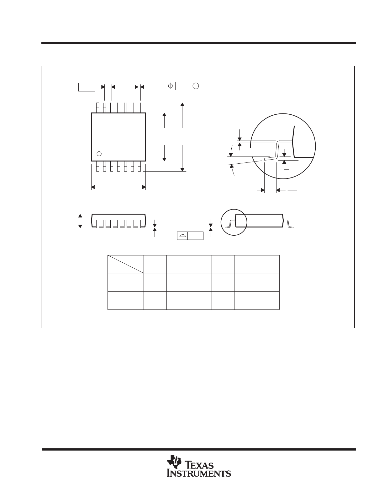
MECHANICAL DATA
MTSS001C – JANUARY 1995 – REVISED FEBRUARY 1999
PW (R-PDSO-G**) PLASTIC SMALL-OUTLINE PACKAGE
14 PINS SHOWN
0,65
1,20 MAX
14
0,30
0,19
8
4,50
4,30
PINS **
7
Seating Plane
0,15
0,05
8
1
A
DIM
14
0,10
6,60
6,20
M
0,10
0,15 NOM
0°–8°
2016
Gage Plane
24
0,25
0,75
0,50
28
A MAX
A MIN
NOTES: A. All linear dimensions are in millimeters.
B. This drawing is subject to change without notice.
C. Body dimensions do not include mold flash or protrusion not to exceed 0,15.
D. Falls within JEDEC MO-153
3,10
2,90
5,10
4,90
5,10
4,90
6,60
6,40
7,90
7,70
9,80
9,60
4040064/F 01/97
POST OFFICE BOX 655303 • DALLAS, TEXAS 75265

IMPORTANT NOTICE
Texas Instruments Incorporated and its subsidiaries (TI) reserve the right to make corrections, modifications, enhancements,
improvements, and other changes to its products and services at any time and to discontinue any product or service without notice.
Customers should obtain the latest relevant information before placing orders and should verify that such information is current and
complete. All products are sold subject to TI’s terms and conditions of sale supplied at the time of order acknowledgment.
TI warrants performance of its hardware products to the specifications applicable at the time of sale in accordance with TI’s
standard warranty. Testing and other quality control techniques are used to the extent TI deems necessary to support this
warranty. Except where mandated by government requirements, testing of all parameters of each product is not necessarily
performed.
TI assumes no liability for applications assistance or customer product design. Customers are responsible for their products and
applications using TI components. To minimize the risks associated with customer products and applications, customers should
provide adequate design and operating safeguards.
TI does not warrant or represent that any license, either express or implied, is granted under any TI patent right, copyright, mask
work right, or other TI intellectual property right relating to any combination, machine, or process in which TI products or services
are used. Information published by TI regarding third-party products or services does not constitute a license from TI to use such
products or services or a warranty or endorsement thereof. Use of such information may require a license from a third party under
the patents or other intellectual property of the third party, or a license from TI under the patents or other intellectual property of TI.
Reproduction of TI information in TI data books or data sheets is permissible only if reproduction is without alteration and is
accompanied by all associated warranties, conditions, limitations, and notices. Reproduction of this information with alteration is an
unfair and deceptive business practice. TI is not responsible or liable for such altered documentation. Information of third parties
may be subject to additional restrictions.
Resale of TI products or services with statements different from or beyond the parameters stated by TI for that product or service
voids all express and any implied warranties for the associated TI product or service and is an unfair and deceptive business
practice. TI is not responsible or liable for any such statements.
TI products are not authorized for use in safety-critical applications (such as life support) where a failure of the TI product would
reasonably be expected to cause severe personal injury or death, unless officers of the parties have executed an agreement
specifically governing such use. Buyers represent that they have all necessary expertise in the safety and regulatory ramifications
of their applications, and acknowledge and agree that they are solely responsible for all legal, regulatory and safety-related
requirements concerning their products and any use of TI products in such safety-critical applications, notwithstanding any
applications-related information or support that may be provided by TI. Further, Buyers must fully indemnify TI and its
representatives against any damages arising out of the use of TI products in such safety-critical applications.
TI products are neither designed nor intended for use in military/aerospace applications or environments unless the TI products are
specifically designated by TI as military-grade or "enhanced plastic." Only products designated by TI as military-grade meet military
specifications. Buyers acknowledge and agree that any such use of TI products which TI has not designated as military-grade is
solely at the Buyer's risk, and that they are solely responsible for compliance with all legal and regulatory requirements in
connection with such use.
TI products are neither designed nor intended for use in automotive applications or environments unless the specific TI products
are designated by TI as compliant with ISO/TS 16949 requirements. Buyers acknowledge and agree that, if they use any
non-designated products in automotive applications, TI will not be responsible for any failure to meet such requirements.
Following are URLs where you can obtain information on other Texas Instruments products and application solutions:
Products Applications
Amplifiers amplifier.ti.com Audio www.ti.com/audio
Data Converters dataconverter.ti.com Automotive www.ti.com/automotive
DSP dsp.ti.com Broadband www.ti.com/broadband
Interface interface.ti.com Digital Control www.ti.com/digitalcontrol
Logic logic.ti.com Military www.ti.com/military
Power Mgmt power.ti.com Optical Networking www.ti.com/opticalnetwork
Microcontrollers microcontroller.ti.com Security www.ti.com/security
RFID www.ti-rfid.com Telephony www.ti.com/telephony
Low Power www.ti.com/lpw Video & Imaging www.ti.com/video
Wireless
Wireless www.ti.com/wireless
Mailing Address: Texas Instruments, Post Office Box 655303, Dallas, Texas 75265
Copyright © 2007, Texas Instruments Incorporated
 Loading...