

Page 1
INA203
INA203
INA203
1
2
3
4
5
10
9
8
7
6
V
IN+
V
IN-
CMP1OUT
CMP2OUT
CMP1 RESET
V
S
OUT
CMP1IN+
CMP2IN+
GND
INA203 INA205-
MSOP-10
0.6VREF
1
2
3
4
5
6
7
14
13
12
11
10
9
8
V
IN+
V
IN-
1.2VREFOUT
CMP1OUT
CMP2OUT
CMP2DELAY
CMP1 RESET
V
S
OUT
CMP1IN /0.6VREF-
CMP1IN+
CMP2IN+
CMP2IN /0.6VREF-
GND
INA203 INA205-
SO-14,TSSOP-14
1.2VREF
INA203
INA204
INA205
SBOS393C – MARCH 2007 – REVISED OCTOBER 2007
Unidirectional Measurement
Current-Shunt Monitor with Dual Comparators
1
FEATURES DESCRIPTION
2
• COMPLETE CURRENT SENSE SOLUTION
• DUAL COMPARATORS:
– Comparator 1 with Latch
– Comparator 2 with Optional Delay
• COMMON-MODE RANGE: – 16V to +80V to +80V. The INA203, INA204, and INA205 are
• HIGH ACCURACY: 3.5% (max) Over
Temperature
• BANDWIDTH: 500kHz
• QUIESCENT CURRENT: 1.8mA
• PACKAGES: SO-14, TSSOP-14, MSOP-10
APPLICATIONS
• NOTEBOOK COMPUTERS
• CELL PHONES
• TELECOM EQUIPMENT
• AUTOMOTIVE
• POWER MANAGEMENT
• BATTERY CHARGERS
• WELDING EQUIPMENT
The INA203, INA204, and INA205 are a family of
unidirectional current-shunt monitors with voltage
output, dual comparators, and voltage reference. The
INA203, INA204, and INA205 can sense drops
across shunts at common-mode voltages from – 16V
available with three output voltage scales: 20V/V,
50V/V, and 100V/V, with up to 500kHz bandwidth.
The INA203, INA204, and INA205 also incorporate
two open-drain comparators with internal 0.6V
references. On 14-pin versions, the comparator
references can be overridden by external inputs.
Comparator 1 includes a latching capability, and
Comparator 2 has a user-programmable delay. 14-pin
versions also provide a 1.2V reference output.
The INA203, INA204, and INA205 operate from a
single +2.7V to +18V supply. They are specified over
the extended operating temperature range of – 40 ° C
to +125 ° C.
1
2 All trademarks are the property of their respective owners.
PRODUCTION DATA information is current as of publication date.
Products conform to specifications per the terms of the Texas
Instruments standard warranty. Production processing does not
necessarily include testing of all parameters.
Please be aware that an important notice concerning availability, standard warranty, and use in critical applications of
Texas Instruments semiconductor products and disclaimers thereto appears at the end of this data sheet.
DEVICE GAIN
INA203 20V/V
INA204 50V/V
INA205 100V/V
RELATED PRODUCTS
FEATURES PRODUCT
Variant of INA203 – INA205 Comparator 2 polarity INA206 – INA208
Current-shunt monitor with single Comparator INA200 – INA202
and V
REF
Current-shunt monitor only INA193 – INA198
Current-shunt monitor with split stages for filter INA270 – INA271
options
Copyright © 2007, Texas Instruments Incorporated
Page 2
www.ti.com
INA203
INA204
INA205
SBOS393C – MARCH 2007 – REVISED OCTOBER 2007
This integrated circuit can be damaged by ESD. Texas Instruments recommends that all integrated circuits be handled with
appropriate precautions. Failure to observe proper handling and installation procedures can cause damage.
ESD damage can range from subtle performance degradation to complete device failure. Precision integrated circuits may be more
susceptible to damage because very small parametric changes could cause the device not to meet its published specifications.
ORDERING INFORMATION
PRODUCT GAIN LEAD DESIGNATOR MARKING REF OUT REF INPUTS 0.6V REF PIN
INA203 20V/V MSOP-10 DGS BQN X
INA204 50V/V MSOP-10 DGS BQO X
INA205 100V/V MSOP-10 DGS BQP X
(1) For the most current package and ordering information see the Package Option Addendum at the end of this document, or see the TI
web site at www.ti.com .
ABSOLUTE MAXIMUM RATINGS
Supply Voltage, V+ 18 V
Current-Shunt Monitor Analog
Inputs, V
Comparator Analog Input and Reset Pins GND – 0.3 to (V+) + 0.3 V
Analog Output, Out Pin GND – 0.3 to (V+) + 0.3 V
Comparator Output, Out Pin GND – 0.3 to 18 V
V
REF
Input Current Into Any Pin 5 mA
Operating Temperature – 55 to +150 ° C
Storage Temperature – 65 to +150 ° C
Junction Temperature +150 ° C
ESD Ratings
(1) Stresses above these ratings may cause permanent damage. Exposure to absolute maximum conditions for extended periods may
and V
IN+
and CMP2 Delay Pin GND – 0.3 to 10 V
degrade device reliability. These are stress ratings only, and functional operation of the device at these or any other conditions beyond
those specified is not supported.
IN –
PACKAGE- PACKAGE PACKAGE 1.2V COMP2 COMP2 DELAY
SO-14 D INA203A X X X X
TSSOP-14 PW INA203A X X X X
SO-14 D INA204A X X X X
TSSOP-14 PW INA204A X X X X
SO-14 D INA205A X X X X
TSSOP-14 PW INA205A X X X X
(1)
Differential (V
Common-Mode – 16 to +80 V
Human Body Model (HBM) 4000 V
Charged Device Model (CDM) 500 V
) – (V
IN+
) – 18 to +18 V
IN –
(1)
EXTERNAL INTERNAL
COMP1 AND COMP1 AND COMP2
INA203, INA204, INA205 UNIT
2 Submit Documentation Feedback Copyright © 2007, Texas Instruments Incorporated
Product Folder Link(s): INA203 INA204 INA205
Page 3
www.ti.com
SBOS393C – MARCH 2007 – REVISED OCTOBER 2007
ELECTRICAL CHARACTERISTICS: CURRENT-SHUNT MONITOR
Boldface limits apply over the specified temperature range: TA= – 40 ° C to +125 ° C.
At TA= +25 ° C, VS= +12V, V
OUT and CMP2 OUT to VS, and CMP1 IN+ = 1V and CMP2 IN – = GND, unless otherwise noted.
CURRENT-SHUNT MONITOR PARAMETERS CONDITIONS MIN TYP MAX UNIT
INPUT
Full-Scale Sense Input Voltage V
Common-Mode Input Range V
Common-Mode Rejection Ratio CMRR VCM= – 16V to +80V 80 100 dB
Over Temperature VCM= +12V to +80V 100 123 dB
Offset Voltage, RTI
+25 ° C to +125 ° C ± 3 mV
– 40 ° C to +25 ° C ± 3.5 mV
vs Temperature dV
vs Power Supply PSR V
Input Bias Current, V
OUTPUT (V
Gain: G
INA203 20 V/V
INA204 50 V/V
INA205 100 V/V
Gain Error V
Over Temperature V
Total Output Error
Over Temperature V
Nonlinearity Error
Output Impedance, Pin 2 R
Maximum Capacitive Load No Sustained Oscillation 10 nF
OUTPUT (V
INA203, INA204, INA205 – 16V ≤ VCM< 0V 300 mV
INA203 0V ≤ VCM≤ VS, VS= 5V 0.4 V
INA204 0V ≤ VCM≤ VS, VS= 5V 1 V
INA205 0V ≤ VCM≤ VS, VS= 5V 2 V
INA203, INA204, INA205 VS< VCM≤ 80V 300 mV
VOLTAGE OUTPUT
Output Swing to the Positive Rail V
Output Swing to GND
FREQUENCY RESPONSE
Bandwidth: BW
INA203 C
INA204 C
INA205 C
Phase Margin C
Slew Rate SR 1 V/ μ s
Settling Time (1%) 2 μ s
NOISE, RTI
Output Voltage Noise Density 40 nV/ √ Hz
(1) Offset is extrapolated from measurements of the output at 20mV and 100mV V
(2) Total output error includes effects of gain error and VOS.
(3) Linearity is best fit to a straight line.
(4) For details on this region of operation, see the Accuracy Variations section in the Applications Information .
(5) See Typical Characteristic curve Positive Output Voltage Swing vs Output Current (Figure 8 ).
(6) Specified by design; not production tested.
(1)
Pin I
IN –
≥ 20mV)
SENSE
(2)
(3)
(4)
< 20mV)
SENSE
(5)
(6)
CM
= +12V, V
SENSE
OS
SENSE
CM
V
OS
/dT T
OUT
B
SENSE
SENSE
V
SENSE
SENSE
V
SENSE
O
V
V
SENSE
= 100mV, RL= 10k Ω to GND, R
= 5.1k Ω each connected from CMP1
PULL-UP
INA203, INA204, INA205
V
= V
SENSE
– V
IN+
IN –
0.15 (V
– 0.25)/Gain V
S
– 16 80 V
± 0.5 ± 2.5 mV
to T
MIN
MAX
5 μ V/ ° C
= 2V, VCM= +18V, 2.7V 2.5 100 μ V/V
± 9 ± 16 μ A
= 20mV to 100mV ± 0.2 ± 1 %
= 20mV to 100mV ± 2 %
= 120mV, VS= +16V ± 0.75 ± 2.2 %
= 120mV, VS= +16V ± 3.5 %
= 20mV to 100mV ± 0.002 %
1.5 Ω
= 11V, V
IN –
= 0V, V
IN –
LOAD
LOAD
LOAD
LOAD
= 10mV
C
LOAD
= 12V (V+) – 0.15 (V+) – 0.25 V
IN+
= – 0.5V (V
IN+
) + 0.004 (V
GND
) + 0.05 V
GND
= 5pF 500 kHz
= 5pF 300 kHz
= 5pF 200 kHz
< 10nF 40 Degrees
to 100mV
PP
= 5pF
,
PP
.
SENSE
INA203
INA204
INA205
Copyright © 2007, Texas Instruments Incorporated Submit Documentation Feedback 3
Product Folder Link(s): INA203 INA204 INA205
Page 4
www.ti.com
INA203
INA204
INA205
SBOS393C – MARCH 2007 – REVISED OCTOBER 2007
ELECTRICAL CHARACTERISTICS: COMPARATOR
Boldface limits apply over the specified temperature range: TA= – 40 ° C to +125 ° C.
At TA= +25 ° C, VS= +12V, V
CMP1 OUT and CMP2 OUT to VS, unless otherwise noted.
COMPARATOR PARAMETERS CONDITIONS MIN TYP MAX UNIT
OFFSET VOLTAGE
Offset Voltage Comparator Common-Mode Voltage = Threshold Voltage 2 mV
Offset Voltage Drift, Comparator 1 ± 2 μ V/ ° C
Offset Voltage Drift, Comparator 2 +5.4 μ V/ ° C
Threshold TA= +25 ° C 590 608 620 mV
Over Temperature 586 625 mV
Hysteresis
Hysteresis
INPUT BIAS CURRENT
CMP1 IN+, CMP2 IN+ 0.005 10 nA
INPUT IMPEDANCE
Pins 3 and 6 (14-pin packages only) 10 k Ω
INPUT RANGE
CMP1 IN+ and CMP2 IN+ 0V to VS– 1.5V V
Pins 3 and 6 (14-pin packages only)
OUTPUT
Large-Signal Differential Voltage Gain CMP V
High-Level Output Current VID= 0.4V, VOH= V
Low-Level Output Voltage VID= – 0.6V, IOL= 2.35mA 220 300 mV
RESPONSE TIME
Comparator 1 RLto 5V, CL= 15pF, 100mV Input Step with 5mV Overdrive 1.3 μ s
Comparator 2 1.3 μ s
RESET
RESET Threshold
Logic Input Impedance 2 M Ω
Minimum RESET Pulse Width 1.5 μ s
RESET Propagation Delay 3 μ s
Comparator 2 Delay Equation
Comparator 2 Delay t
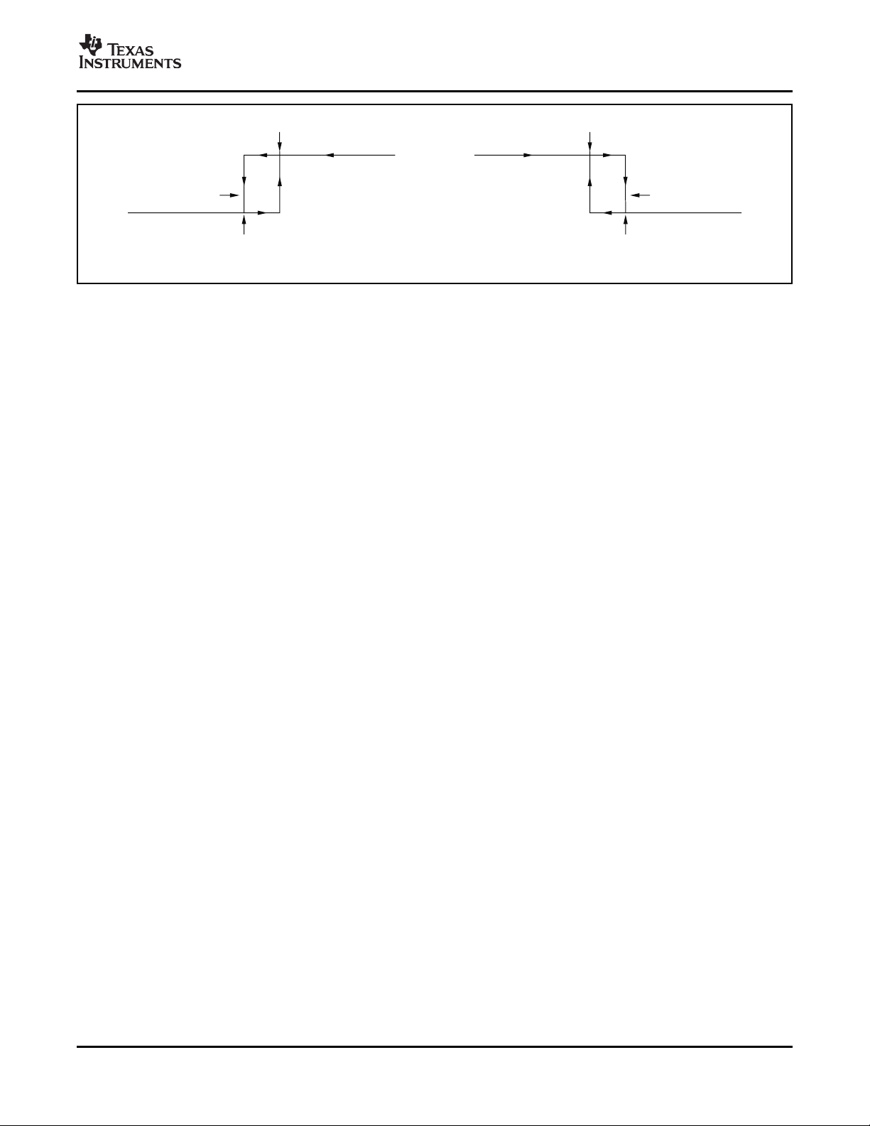
(1) Hysteresis refers to the threshold (the threshold specification applies to a rising edge of a noninverting input) of a falling edge on the
(2) Specified by design; not production tested.
(3) See the Comparator Maximum Input Voltage Range section in the Applications Information .
(4) The comparator response time specified is the interval between the input step function and the instant when the output crosses 1.4V.
(5) The CMP1 RESET input has an internal 2M Ω (typical) pull-down. Leaving the CMP1 RESET open results in a LOW state, with
(6) The Comparator 2 delay applies to both rising and falling edges of the comparator output.
(1)
, CMP1 TA= – 40 ° C to +85 ° C – 8 mV
(1)
, CMP2 TA= – 40 ° C to +85 ° C 8 mV
vs Temperature 15 nA
(2)
(4)
(5)
(6)
noninverting input of the comparator; refer to Figure 1 .
transparent comparator operation.
CM
(3)
= +12V, V
RLto 5V, CL= 15pF, 100mV Input Step with 5mV Overdrive,
D
= 100mV, RL= 10k Ω to GND, and R
SENSE
1V to 4V, RL≥ 15k Ω Connected to 5V 200 V/mV
OUT
C
DELAY
C
= 5.1k Ω each connected from
PULL-UP
INA203, INA204, INA205
0V to VS– 1.5V V
S
Pin Open
= 0.1 μ F 0.5 s
DELAY
0.0001 1 μ A
1.1 V
C
= tD/5 μ F
DELAY
4 Submit Documentation Feedback Copyright © 2007, Texas Instruments Incorporated
Product Folder Link(s): INA203 INA204 INA205
Page 5
www.ti.com
Hysteresis=V
THRESHOLD
- 8mV
V
THRESHOLD
InputVoltage
0.592 0.6
a) CMP1
Hysteresis=V
THRESHOLD
- 8mV
V
THRESHOLD
InputVoltage
0.6080.6
b) CMP2
Figure 1. Comparator Hysteresis
INA203
INA204
INA205
SBOS393C – MARCH 2007 – REVISED OCTOBER 2007
Copyright © 2007, Texas Instruments Incorporated Submit Documentation Feedback 5
Product Folder Link(s): INA203 INA204 INA205
Page 6
www.ti.com
INA203
INA204
INA205
SBOS393C – MARCH 2007 – REVISED OCTOBER 2007
ELECTRICAL CHARACTERISTICS: REFERENCE
Boldface limits apply over the specified temperature range: TA= – 40 ° C to +125 ° C.
At TA= +25 ° C, VS= +12V, V
CMP1 OUT and CMP2 OUT to VS, unless otherwise noted.
REFERENCE PARAMETERS CONDITIONS MIN TYP MAX UNIT
REFERENCE VOLTAGE
1.2V
Reference Drift dV
0.6V
Reference Drift dV
LOAD REGULATION dV
Sourcing 0mA < I
Sinking 0mA < I
LOAD CURRENT I
LINE REGULATION dV
CAPACITIVE LOAD
Reference Output Maximum Capacitive Load No Sustained Oscillations 10 nF
OUTPUT IMPEDANCE
Pins 3 and 6 of 14-Pin Packages Only 10 k Ω
Output Voltage 1.188 1.2 1.212 V
REFOUT
Output Voltage (Pins 3 and 6 of 14-pin packages only) 0.6 V
REF
CM
= +12V, V
= 100mV, RL= 10k Ω to GND, and R
SENSE
/dT TA= – 40 ° C to +85 ° C 40 100 ppm/ ° C
OUT
/dT TA= – 40 ° C to +85 ° C 40 100 ppm/ ° C
OUT
/dI
OUT
LOAD
LOAD
/dV
OUT
S
= 5.1k Ω each connected from
PULL-UP
INA203, INA204, INA205
< 0.5mA 0.4 2 mV/mA
SOURCE
< 0.5mA 0.4 mV/mA
SINK
1 mA
2.7V < VS< 18V 30 μ V/V
ELECTRICAL CHARACTERISTICS: GENERAL
Boldface limits apply over the specified temperature range: TA= – 40 ° C to +125 ° C.
All specifications at TA= +25 ° C, VS= +12V, V
connected from CMP1 OUT and CMP2 OUT to VS, and CMP1 IN+ = 1V and CMP2 IN – = GND, unless otherwise noted.
GENERAL PARAMETERS CONDITIONS MIN TYP MAX UNIT
POWER SUPPLY
Operating Power Supply V
Quiescent Current I
Over Temperature V
Comparator Power-On Reset Threshold
TEMPERATURE
Specified Temperature Range – 40 +125 ° C
Operating Temperature Range – 55 +150 ° C
Storage Temperature Range – 65 +150 ° C
Thermal Resistance θ
MSOP-10 Surface-Mount 200 ° C/W
SO-14, TSSOP-14 Surface-Mount 150 ° C/W
(1) The INA203, INA204, and INA205 are designed to power-up with the comparator in a defined reset state as long as CMP1 RESET is
open or grounded. The comparator will be in reset as long as the power supply is below the voltage shown here. The comparator
assumes a state based on the comparator input above this supply voltage. If CMP1 RESET is high at power-up, the comparator output
comes up high and requires a reset to assume a low state, if appropriate.
(1)
CM
= +12V, V
= 100mV, RL= 10k Ω to GND, R
SENSE
= 5.1k Ω each
PULL-UP
INA203, INA204, INA205
S
V
Q
= 2V 1.8 2.2 mA
OUT
= 0mV 2.8 mA
SENSE
+2.7 +18 V
1.5 V
JA
6 Submit Documentation Feedback Copyright © 2007, Texas Instruments Incorporated
Product Folder Link(s): INA203 INA204 INA205
Page 7
www.ti.com
TYPICAL CHARACTERISTICS
45
40
35
30
25
20
15
10
5
10k
100k
Gain(dB)
Frequency(Hz)
1M
G=100
C =1000pF
LOAD
G=50
G=20
45
40
35
30
25
20
15
10
5
10k
100k
Gain(dB)
Frequency(Hz)
1M
G=100
G=50
G=20
C =0
LOAD
20
18
16
14
12
10
8
6
4
2
0
20
100
200 300 400
500 600 700
V
(V)
OU
T
V (mV)
SENSE
800 900
50V/V
20V/V
100V/V
140
130
120
110
100
90
80
70
60
50
40
10
100 1k 10k
Common-Modeand
P
ower
-SupplyRejection(dB)
Frequency(Hz)
100k
CMR
PSR
4.0
3.5
3.0
2.5
2.0
1.5
1.0
0.5
0
0
50
100
150 200
250 300
350
TotalOutputError
(%erroroftheidealoutputvalue)
V (mV)
SENSE
400 450
500
0.1
0.09
0.08
0.07
0.06
0.05
0.04
0.03
0.02
0.01
0
-16
-12
-8
-4 0
4 128
2016
T
otalOutputError(%)
Common-ModeVoltage(V)
... 76
80
All specifications at TA= +25 ° C, VS= +12V, V
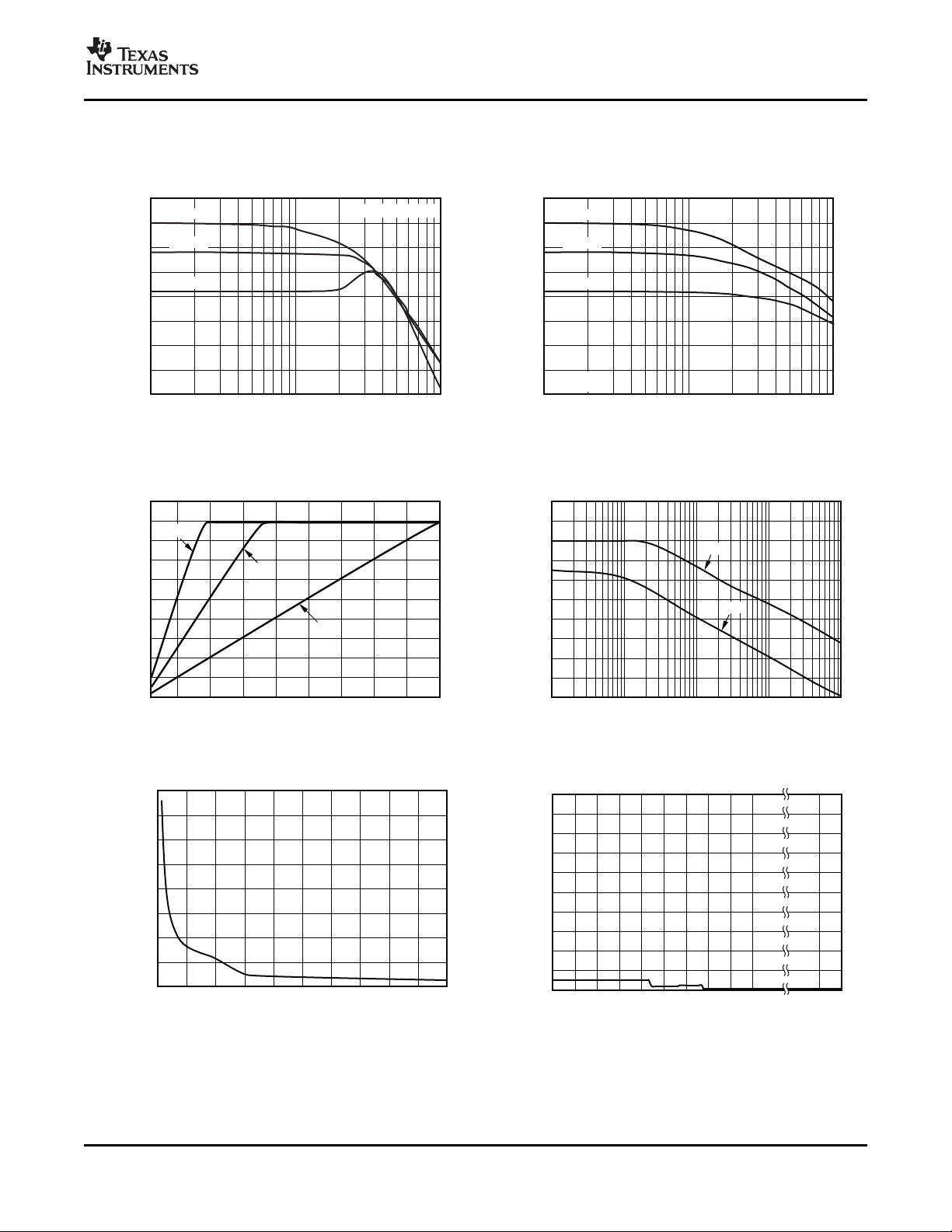
GAIN vs FREQUENCY GAIN vs FREQUENCY
Figure 2. Figure 3.
= +12V, and V
CM
SBOS393C – MARCH 2007 – REVISED OCTOBER 2007
= 100mV, unless otherwise noted.
SENSE
INA203
INA204
INA205
GAIN PLOT vs FREQUENCY
Figure 4. Figure 5.
TOTAL OUTPUT ERROR vs V
COMMON-MODE AND POWER-SUPPLY REJECTION
SENSE
TOTAL OUTPUT ERROR vs COMMON-MODE VOLTAGE
Copyright © 2007, Texas Instruments Incorporated Submit Documentation Feedback 7
Figure 6. Figure 7.
Product Folder Link(s): INA203 INA204 INA205
Page 8
www.ti.com
12
11
10
9
8
7
6
5
4
3
2
1
0
0
5
10
15
20
OutputVoltage(V)
OutputCurrent(mA)
25
30
V =12V
S
+25 C°
+25 C°
- °40 C
- °40 C
+125 C°
+125 C°
SourcingCurrent
V =3V
S
SourcingCurrent
Outputstageisdesigned
tosourcecurrent.Current
sinkingcapabilityis
approximately400 A.m
3.5
3.0
2.5
2.0
1.5
1.0
0.5
0
0
1
2
3 4
5 6
7
I (mA)
Q
OutputVoltage(V)
8 9
10
2.00
1.75
1.50
1.25
1.00
0.75
0.50
-16
-12
-8
-4 0 4
8 12 16
20 24 28
I
(mA)
Q
V (V)
CM
32
36
V =0mV
SENSE
V =12V
S
V =2.7V
S
V =100mV
SENSE
V =12V
S
V =2.7V
S
34
30
26
22
18
14
10
6
2.5
3.5
4.5 5.5 6.5
7.5 8.5 9.5
10.5
OutputShort-CircuitCurrent(mA)
SupplyVoltage(V)
11.5 17
18
- °40 C
+ °25 C
+125 C°
OutputVoltage(50mV/div)
Time(2 s/div)m
G=20
V =10mVto20mV
SENSE
Time(2 s/div)m
G=20
OutputVoltage(500mV/div)
V =10mVto100mV
SENSE
INA203
INA204
INA205
SBOS393C – MARCH 2007 – REVISED OCTOBER 2007
TYPICAL CHARACTERISTICS (continued)
All specifications at TA= +25 ° C, VS= +12V, V
POSITIVE OUTPUT VOLTAGE SWING
vs OUTPUT CURRENT QUIESCENT CURRENT vs OUTPUT VOLTAGE
Figure 8. Figure 9.
= +12V, and V
CM
= 100mV, unless otherwise noted.
SENSE
QUIESCENT CURRENT OUTPUT SHORT-CIRCUIT CURRENT
vs COMMON-MODE VOLTAGE vs SUPPLY VOLTAGE
Figure 10. Figure 11.
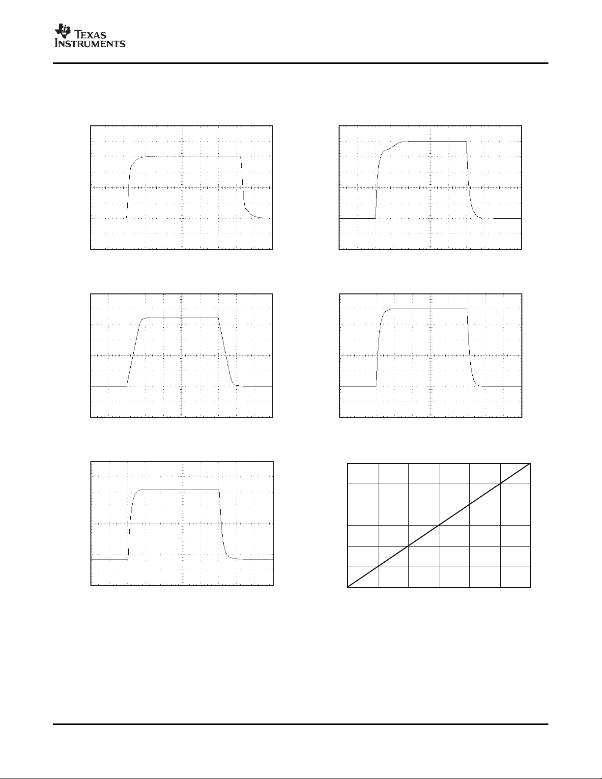
STEP RESPONSE STEP RESPONSE
8 Submit Documentation Feedback Copyright © 2007, Texas Instruments Incorporated
Figure 12. Figure 13.
Product Folder Link(s): INA203 INA204 INA205
Page 9
www.ti.com
Time(2 s/div)m
G=20
OutputVoltage(50mV/div)
V =90mVto100mV
SENSE
Time(5 s/div)m
G=50
OutputVoltage(100mV/div)
V =10mVto20mV
SENSE
Time(5 s/div)m
G=50
OutputVoltage(1V/div)
V =10mVto100mV
SENSE
Time(5 s/div)m
G=50
OutputVoltage(100mV/div)
V =90mVto100mV
SENSE
Time(10 s/div)m
G=100
OutputVoltage(2V/div)
V =10mVto100mV
SENSE
600
500
400
300
200
100
0
0
1
2 3 4
5
V (mV)
OL
I (mA)
SINK
6
TYPICAL CHARACTERISTICS (continued)
All specifications at TA= +25 ° C, VS= +12V, V
STEP RESPONSE STEP RESPONSE
Figure 14. Figure 15.
STEP RESPONSE STEP RESPONSE
= +12V, and V
CM
= 100mV, unless otherwise noted.
SENSE
INA203
INA204
INA205
SBOS393C – MARCH 2007 – REVISED OCTOBER 2007
Figure 16. Figure 17.
STEP RESPONSE COMPARATOR V
Figure 18. Figure 19.
vs I
OL
SINK
Copyright © 2007, Texas Instruments Incorporated Submit Documentation Feedback 9
Product Folder Link(s): INA203 INA204 INA205
Page 10

www.ti.com
600
599
598
597
596
595
594
593
592
591
590
2
4
6 8 10
12 14 16
ComparatorT
ripPoint(mV)
SupplyVoltage(V)
18
602
601
600
599
598
597
596
-50
-25
0 25 50
75 100
ComparatorT
ripPoint(mV)
Temperature( C)°
125
200
175
150
125
100
75
50
0
20
40 60 80
100 120 140 160 180
PropagationDelay(ns)
OverdriveVoltage(mV)
200
14
13
12
11
10
0
20
40 60 80
100 120 140 160 180
PropagationDelay( s)m
OverdriveVoltage(mV)
200
1.2
1.0
0.8
0.6
0.4
0.2
0
2
4
6 8 10
12 14 16
ResetVoltage(V)
SupplyVoltage(V)
18
300
275
250
225
200
175
150
125
-50
-25
0 25 50
75 100
PropagationDelay(ns)
Temperature( C)°
125
INA203
INA204
INA205
SBOS393C – MARCH 2007 – REVISED OCTOBER 2007
TYPICAL CHARACTERISTICS (continued)
All specifications at TA= +25 ° C, VS= +12V, V
COMPARATOR TRIP POINT vs SUPPLY VOLTAGE COMPARATOR TRIP POINT vs TEMPERATURE
Figure 20. Figure 21.
COMPARATOR 1 PROPAGATION DELAY COMPARATOR 2 PROPAGATION DELAY
vs OVERDRIVE VOLTAGE vs OVERDRIVE VOLTAGE
= +12V, and V
CM
= 100mV, unless otherwise noted.
SENSE
10 Submit Documentation Feedback Copyright © 2007, Texas Instruments Incorporated
COMPARATOR RESET VOLTAGE vs COMPARATOR 1 PROPAGATION DELAY vs
Figure 22. Figure 23.
SUPPLY VOLTAGE TEMPERATURE
Figure 24. Figure 25.
Product Folder Link(s): INA203 INA204 INA205
Page 11

www.ti.com
Input
200mV/div
Output
2V/div
2 s/divm
V =5mV
OD
1000
100
10
1
0.1
0.01
0.001
0.01
0.1 1 10
PropagationDelay(ms)
DelayCapacitance(nF)
100
Input
200mV/div
Output
2V/div
5 s/divm
V =5mV
OD
1.22
1.21
1.20
1.19
1.18
-50
-25
0 25 50
75 100
V (V)
REF
Temperature( C)°
125
TYPICAL CHARACTERISTICS (continued)
All specifications at TA= +25 ° C, VS= +12V, V
= +12V, and V
CM
= 100mV, unless otherwise noted.
SENSE
INA203
INA204
INA205
SBOS393C – MARCH 2007 – REVISED OCTOBER 2007
COMPARATOR 2 PROPAGATION DELAY
vs CAPACITANCE COMPARATOR 1 PROPAGATION DELAY
Figure 26. Figure 27.
COMPARATOR 2 PROPAGATION DELAY REFERENCE VOLTAGE vs TEMPERATURE
Copyright © 2007, Texas Instruments Incorporated Submit Documentation Feedback 11
Figure 28. Figure 29.
Product Folder Link(s): INA203 INA204 INA205
Page 12

www.ti.com
G=
V V-
OUT1 OUT2
100mV 20mV-
V RTI(Referred-To-Input)=
OS
V
OUT1
G
- 100mV
INA203
x20
R
SHUNT
3mW
LoadSupply
-18Vto+80V
Load
5VSupply
OptionalDelay
Capacitor
0.2 Fm
C
BYPASS
0.01 Fm
V
S
OUT
CMP1IN /0.6REF-
CMP1IN+
CMP2IN+
CMP2IN /0.6REF-
GND
V
IN+
V
IN-
1.2VREFOUT
CMP1OUT
CMP2OUT
CMP2DELAY
CMP1
RESET
CurrentShunt
MonitorOutput
1.2VREF
R
PULL-UP
4.7kW
R
PULL-UP
4.7kW
Transparent/Reset
Latch
INA203
INA204
INA205
SBOS393C – MARCH 2007 – REVISED OCTOBER 2007
APPLICATIONS INFORMATION
BASIC CONNECTIONS
Figure 30 shows the basic connections of the
INA203, INA204, and INA205. The input pins, V
and V
, should be connected as closely as possible
IN –
IN+
to the shunt resistor to minimize any resistance in
series with the shunt resistance.
Power-supply bypass capacitors are required for
stability. Applications with noisy or high-impedance
power supplies may require additional decoupling
capacitors to reject power-supply noise. Connect • Low V
bypass capacitors close to the device pins. 80V
This section addresses the accuracy of these specific
operating regions:
• Normal Case 1: V
• Normal Case 2: V
• Low V
< 0
• Low V
V
S
≥ 20mV, V
SENSE
≥ 20mV, V
SENSE
Case 1: V
SENSE
Case 2: V
SENSE
Case 3: V
SENSE
< 20mV, – 16V ≤ V
SENSE
< 20mV, 0V ≤ V
SENSE
< 20mV, V
SENSE
≥ V
CM
S
< V
CM
S
CM
≤
CM
< V
S
≤
CM
POWER SUPPLY
The input circuitry of the INA203, INA204, and
INA205 can accurately measure beyond the
power-supply voltage, V+. For example, the V+ power
supply can be 5V, whereas the load power-supply
voltage is up to +80V. The output voltage range of
the OUT terminal, however, is limited by the voltages
on the power-supply pin.
ACCURACY VARIATIONS AS A RESULT OF
V
The accuracy of the INA203, INA204, and INA205
current shunt monitors is a function of two main
variables: V
voltage, V
expressed as (V
V
voltage drop across V
AND COMMON-MODE VOLTAGE
SENSE
(V
SENSE
, relative to the supply voltage, VS. V
CM
is seen as the voltage at V
CM
IN+
+ V
IN+
SENSE
– V
IN –
)/2; however, in practice,
IN –
is usually small.
) and common-mode
because the
IN+
Normal Case 1: V
≥ 20mV, V
SENSE
≥ V
CM
S
This region of operation provides the highest
accuracy. Here, the input offset voltage is
characterized and measured using a two-step
method. First, the gain is determined by Equation 1 .
(1)
where:
V
= Output Voltage with V
OUT1
V
= Output Voltage with V
OUT2
Then the offset voltage is measured at V
= 100mV
SENSE
= 20mV
SENSE
=
SENSE
100mV and referred to the input (RTI) of the current
is
CM
shunt monitor, as shown in Equation 2 .
(2)
12 Submit Documentation Feedback Copyright © 2007, Texas Instruments Incorporated
Figure 30. INA20x Basic Connection
Product Folder Link(s): INA203 INA204 INA205
Page 13

www.ti.com
2.0
1.8
1.6
1.4
1.2
1.0
0.8
0.6
0.4
0.2
0
0
2
4 6 8
10 12 14 16 18
V (V)
O
UT
V (mV)
SENSE
20
Actual
Ideal
In the Typical Characteristics , the Output Error vs
Common-Mode Voltage curve (Figure 7 ) shows the
highest accuracy for this region of operation. In this
plot, V
= 12V; for V
S
≥ 12V, the output error is at its
CM
minimum. This case is also used to create the
V
≥ 20mV output specifications in the Electrical
SENSE
Characteristics table.
INA203
INA204
INA205
SBOS393C – MARCH 2007 – REVISED OCTOBER 2007
Normal Case 2: V
≥ 20mV, V
SENSE
< V
CM
S
This region of operation has slightly less accuracy
than Normal Case 1 as a result of the common-mode
operating area in which the part functions, as seen in
the Output Error vs Common-Mode Voltage curve
(Figure 7 ). As noted, for this graph V
< 12V, the Output Error increases as V
= 12V; for V
S
CM
becomes
less than 12V, with a typical maximum error of
0.005% at the most negative V
Low V
V
SENSE
Low V
V
SENSE
Case 1:
SENSE
< 20mV, – 16V ≤ V
SENSE
< 20mV, V
Case 3:
< V
S
CM
≤ 80V
= – 16V.
CM
< 0; and
CM
Although the INA203 family of devices are not
designed for accurate operation in either of these
regions, some applications are exposed to these
conditions; for example, when monitoring power
supplies that are switched on and off while V
is still
S
applied to the INA203, INA204, or INA205. It is
important to know what the behavior of the devices
will be in these regions.
As V
approaches 0mV, in these V
SENSE
regions,
CM
the device output accuracy degrades. A
larger-than-normal offset can appear at the current
shunt monitor output with a typical maximum value of
V
approaches 20mV, V
= 300mV for V
OUT
OUT
SENSE
= 0mV. As V
returns to the expected
SENSE
output value with accuracy as specified in the
Electrical Characteristics . Figure 31 illustrates this
effect using the INA205 (Gain = 100).
CM
Figure 31. Example for Low V
SENSE
Cases 1 and 3
(INA205, Gain = 100)
Low V
Case 2: V
SENSE
SENSE
< 20mV, 0V ≤ V
≤ V
CM
S
This region of operation is the least accurate for the
INA203 family. To achieve the wide input
common-mode voltage range, these devices use two
op amp front ends in parallel. One op amp front end
operates in the positive input common-mode voltage
range, and the other in the negative input region. For
this case, neither of these two internal amplifiers
dominates and overall loop gain is very low. Within
this region, V
approaches voltages close to linear
OUT
operation levels for Normal Case 2. This deviation
from linear operation becomes greatest the closer
V
approaches 0V. Within this region, as V
SENSE
SENSE
approaches 20mV, device operation is closer to that
described by Normal Case 2. Figure 32 illustrates this
behavior for the INA205. The V
maximum peak for
OUT
this case is tested by maintaining a constant VS,
setting V
VS. The exact V
test varies from part to part, but the V
peak is tested to be less than the specified V
= 0mV, and sweeping V
SENSE
CM
at which V
peaks during this
OUT
CM
OUT
from 0V to
maximum
OUT
Tested Limit.
Copyright © 2007, Texas Instruments Incorporated Submit Documentation Feedback 13
Product Folder Link(s): INA203 INA204 INA205
Page 14

www.ti.com
2.4
2.2
2.0
1.8
1.6
1.4
1.2
1.0
0.8
0.6
0.4
0.2
0
0
2
4 6 8
10 12 14 16 18 20 22
V (V)
OUT
V (mV)
SENSE
24
INA205V TestedLimit
OUT
(1)
V
CM2
V
CM1
V
CM3
V
CM4
V ,V ,andV
CM2 CM3 CM4
illustratethevariance
fromparttopartoftheV thatcancause
CM
maximumV withV <20mV.
OUT SENSE
V TestedLimitat
OUT
V =0mV,0 V£
CM1
SENSE
V£
.
S
NOTE:(1)INA203V TestedLimit=0.4V.INA204V TestedLimit=1V.
OUT OUT
Ideal
GainError%=100 -
5kW
5k +RW
FILT
100 ´
INA203
INA204
INA205
SBOS393C – MARCH 2007 – REVISED OCTOBER 2007
Figure 32. Example for Low V
(INA205, Gain = 100)
SELECTING R
SHUNT
The value chosen for the shunt resistor, R
depends on the application and is a compromise
between small-signal accuracy and maximum
permissible voltage loss in the measurement line.
High values of R
SHUNT
provide better accuracy at
lower currents by minimizing the effects of offset,
while low values of R
minimize voltage loss in
SHUNT
the supply line. For most applications, best
performance is attained with an R
provides a full-scale shunt voltage range of 50mV to
100mV. Maximum input voltage for accurate
measurements is (V
– 0.25)/Gain.
SHUNT
TRANSIENT PROTECTION
The – 16V to +80V common-mode range of the
INA203, INA204, and INA205 is ideal for withstanding
automotive fault conditions ranging from 12V battery
reversal up to +80V transients, since no additional
protective components are needed up to those levels.
In the event that the INA203, INA204, and INA205
are exposed to transients on the inputs in excess of
their ratings, then external transient absorption with
semiconductor transient absorbers (zeners or
Transzorbs) are necessary. Use of metal oxide
varistors (MOVs) or video disk recorders (VDRs) is
not recommended except when they are used in
addition to a semiconductor transient absorber.
Select the transient absorber such that it will never
allow the INA203, INA204, and INA205 to be
exposed to transients greater than +80V (that is,
14 Submit Documentation Feedback Copyright © 2007, Texas Instruments Incorporated
SENSE
SHUNT
allow for transient absorber tolerance, as well as
additional voltage because of transient absorber
dynamic impedance). Despite the use of internal
zener-type ESD protection, the INA203, INA204, and
INA205 do not lend themselves to using external
resistors in series with the inputs because the internal
gain resistors can vary up to ± 30% but are closely
matched. (If gain accuracy is not important, then
resistors can be added in series with the INA203,
INA204, and INA205 inputs with two equal resistors
on each input.)
OUTPUT VOLTAGE RANGE
The output of the INA203, INA204, and INA205 is
accurate within the output voltage swing range set by
the power-supply pin, V+. This performance is best
Case 2
SHUNT
value that
Product Folder Link(s): INA203 INA204 INA205
illustrated when using the INA205 (a gain of 100
version), where a 100mV full-scale input from the
shunt resistor requires an output voltage swing of
+10V, and a power-supply voltage sufficient to
achieve +10V on the output.
,
INPUT FILTERING
An obvious and straightforward location for filtering is
at the output of the INA203, INA204, and INA205
series; however, this location negates the advantage
of the low output impedance of the internal buffer.
The only other option for filtering is at the input pins
of the INA203, INA204, and INA205, which is
complicated by the internal 5k Ω + 30% input
impedance; this configuration is illustrated in
Figure 33 . Using the lowest possible resistor values
minimizes both the initial shift in gain and effects of
tolerance. The effect on initial gain is given by
Equation 3 :
Total effect on gain error can be calculated by
replacing the 5k Ω term with 5k Ω – 30%, (or 3.5k Ω ) or
5k Ω + 30% (or 6.5k Ω ). The tolerance extremes of
R
FILT
of 100 Ω 1% resistors are used on the inputs, the
initial gain error will be 1.96%. Worst-case tolerance
conditions will always occur at the lower excursion of
the internal 5k Ω resistor (3.5k Ω ), and the higher
excursion of R
can also be inserted into the equation. If a pair
– 3% in this case.
FILT
(3)
Page 15

www.ti.com
R <<R
SHUNT FILTER
3mW
V
SUPPLY
Load
R <100W
FILTER
R <100W
FILTER
C
FILTER
1
2
3
4
5
6
7
14
13
12
11
10
9
8
1.2VREFOUT
CMP1OUT
CMP2OUT
CMP2DELAY
CMP1 RESET
V
IN+
V
IN-
V
S
OUT
CMP1IN /0.6VREF-
CMP1IN+
CMP2IN+
CMP2IN /0.6VREF-
GND
INA203 INA205-
SO-14,TSSOP-14
1.2VREF
f =
-3dB
1
2 (2R )Cp
FILTER FILTER
f
-3dB
C (in F)=m
DELAY
t
D
5
Figure 33. Input Filter (Gain Error: 1.5% to – 2.2%)
INA203
INA204
INA205
SBOS393C – MARCH 2007 – REVISED OCTOBER 2007
Note that the specified accuracy of the INA203, INA205 include additional features for comparator
INA204, and INA205 must then be combined in functions. The comparator reference voltage of both
addition to these tolerances. While this discussion Comparator 1 and Comparator 2 can be overridden
treated accuracy worst-case conditions by combining by external inputs for increased design flexibility.
the extremes of the resistor values, it is appropriate to Comparator 2 has a programmable delay.
use geometric mean or root sum square calculations
to total the effects of accuracy variations.
REFERENCE
COMPARATOR DELAY (14-Pin Version Only)
The Comparator 2 programmable delay is controlled
by a capacitor connected to the CMP2 Delay Pin; see
The INA203, INA204, and INA205 include an internal Figure 30 . The capacitor value (in μ F) is selected by
voltage reference that has a load regulation of using Equation 4 :
0.4mV/mA (typical), and not more than 100ppm/ ° C of
drift. Only the 14-pin package allows external access
to reference voltages, where voltages of 1.2V and
0.6V are both available. Output current versus output A simplified version of the delay circuit for
voltage is illustrated in the Typical Characteristics Comparator 2 is shown in Figure 34 . The delay
section. comparator consists of two comparator stages with
the delay between them. Note that I1 and I2 cannot
COMPARATOR
The INA203, INA204, and INA205 devices
incorporate two open-drain comparators. These
comparators typically have 2mV of offset and a 1.3 μ s
(typical) response time. The output of Comparator 1
latches and is reset through the CMP1 RESET pin,
as shown in Figure 35 . This configuration applies to
both the 10- and 14-pin versions. Figure 34 illustrates
the comparator delay.
The 14-pin versions of the INA203, INA204, and
Copyright © 2007, Texas Instruments Incorporated Submit Documentation Feedback 15
Product Folder Link(s): INA203 INA204 INA205
be turned on simultaneously; I1 corresponds to a U1
low output and I2 corresponds to a U1 high output.
Using an initial assumption that the U1 output is low,
I1 is on, then U2 +IN is zero. If U1 goes high, I2
supplies 120nA to C
. The voltage at U2 +IN
DELAY
begins to ramp toward a 0.6V threshold. When the
voltage crosses this threshold, the U2 output goes
high while the voltage at U2 +IN continues to ramp up
to a maximum of 1.2V when given sufficient time
(twice the value of the delay specified for C
This entire sequence is reversed when the
comparator outputs go low, so that returning to low
exhibits the same delay.
(4)
).
DELAY
Page 16

www.ti.com
U2
U1
0.6V
1.2V
I2
120nA
I1
120nA
C
DELAY
0V
0.6V
V
IN
CMPOut
RESET
20kW 20kW
CMP2IN+
CMP1IN-
1.2V
£ 1mA
INA203
INA204
INA205
SBOS393C – MARCH 2007 – REVISED OCTOBER 2007
Figure 34. Simplified Model of the Comparator 2 Delay Circuit
Figure 35. Comparator Latching Capability
It is important to note what will happen if events occur whether either or both inputs are subject to the large
more rapidly than the delay timeout; for example, voltage. When making this determination, consider
when the U1 output goes high (turning on I2), but the 20k Ω from each input back to the comparator.
returns low (turning I1 back on) prior to reaching the Figure 37 shows the maximum input voltage that
0.6V transition for U2. The voltage at U2 +IN ramps avoids creating a reference error when driving both
back down at a rate determined by the value of inputs (an equivalent resistance back into the
C
, and only returns to zero if given sufficient reference of 10k Ω ).
DELAY
time.
In essence, when analyzing Comparator 2 for
behavior with events more rapid than its delay
setting, use the model shown in Figure 34 .
COMPARATOR MAXIMUM INPUT VOLTAGE RANGE
The maximum voltage at the comparator input for
normal operation is up to (V+) – 1.5V. There are
special considerations when overdriving the reference
inputs (pins 3 and 6). Driving either or both inputs
high enough to drive 1mA back into the reference
introduces errors into the reference. Figure 36 shows
the basic input structure. A general guideline is to
limit the voltage on both inputs to a total of 20V. The
exact limit depends on the available voltage and
16 Submit Documentation Feedback Copyright © 2007, Texas Instruments Incorporated
Product Folder Link(s): INA203 INA204 INA205
Figure 36. Limit Current Into Reference ≤ 1mA
Page 17

www.ti.com
INA203
x20
R
SHUNT
3mW
LoadSupply
-18Vto+80V
Load
5VSupply
OptionalDelay
Capacitor
0.2 Fm
C
BYPASS
0.01 Fm
V
S
OUT
CMP1IN /0.6REF-
CMP1IN+
CMP2IN+
CMP2IN-
GND
V
IN+
V
IN-
1.2VREFOUT
CMP1OUT
CMP2OUT
CMP2DELAY
CMP1
RESET
CurrentShuntMonitorOutput
1.2VREF
R
PULL-UP
4.7kW
R
PULL-UP
4.7kW
Transparent/Reset
Latch
V<11.2
V
IN+
V
IN-
1.2VREFOUT
CMP1OUT
CMP2OUT
CMP2DELAY
CMP1
RESET
V
S+
OUT
CMP1IN-
CMP1IN+
CMP2IN+
CMP2IN-
GND
Load
Overlimit
(1)
Raychem
Polyswitch
Warning
(1)
+5VSupply
3.3kW
Pull-Up
Resistors
C
BYPASS
0.01 Fm
Optional
C
DELAY
0.01 Fm
<18V
Battery
Reset
Latch
NOTE:(1)Warningathalfcurrent(withoptionaldelay).OverlimitlatcheswhenPolyswitchopens.
INA203
x20
1.2VREF
SBOS393C – MARCH 2007 – REVISED OCTOBER 2007
Figure 37. Overdriving Comparator Inputs Without Generating a Reference Error
INA203
INA204
INA205
Figure 38. Polyswitch Warning and Fault Detection Circuit
Copyright © 2007, Texas Instruments Incorporated Submit Documentation Feedback 17
Product Folder Link(s): INA203 INA204 INA205
Page 18

www.ti.com
INA203
x20
V
IN+
V
IN-
1.2VREFOUT
CMP1OUT
CMP2OUT
CMP2DELAY
CMP1
RESET
V
S+
OUT
CMP1IN-
CMP1IN+
CMP2IN+
CMP2IN-
GND
1.2VREF
Load
R
SHUNT
0.02W
+5VSupply
R
3
14kW
R
4
6.04kW
R
5
100kW
R
6
6.04kW
C
BYPASS
0.01 Fm
Q2
NDS8434A
Q1
2N3904
R
1
100kW
Latch
Reset
R
2
1kW
R
7
1kW
INA203
INA204
INA205
SBOS393C – MARCH 2007 – REVISED OCTOBER 2007
Figure 39. Lead-Acid Battery Protection Circuit
18 Submit Documentation Feedback Copyright © 2007, Texas Instruments Incorporated
Product Folder Link(s): INA203 INA204 INA205
Page 19

PACKAGE OPTION ADDENDUM
www.ti.com
PACKAGING INFORMATION
Orderable Device Status
INA203AID ACTIVE SOIC D 14 50 Green (RoHS &
INA203AIDG4 ACTIVE SOIC D 14 50 Green (RoHS &
INA203AIDGSR ACTIVE MSOP DGS 10 2500 Green (RoHS &
INA203AIDGSRG4 ACTIVE MSOP DGS 10 2500 Green (RoHS &
INA203AIDGST ACTIVE MSOP DGS 10 250 Green (RoHS &
INA203AIDGSTG4 ACTIVE MSOP DGS 10 250 Green (RoHS &
INA203AIDR ACTIVE SOIC D 14 2500 Green (RoHS &
INA203AIDRG4 ACTIVE SOIC D 14 2500 Green (RoHS &
INA203AIPW ACTIVE TSSOP PW 14 90 Green (RoHS &
INA203AIPWG4 ACTIVE TSSOP PW 14 90 Green (RoHS &
INA203AIPWR ACTIVE TSSOP PW 14 2000 Green (RoHS &
INA203AIPWRG4 ACTIVE TSSOP PW 14 2000 Green (RoHS &
INA204AID ACTIVE SOIC D 14 50 Green (RoHS &
INA204AIDG4 ACTIVE SOIC D 14 50 Green (RoHS &
INA204AIDGSR ACTIVE MSOP DGS 10 2500 Green (RoHS &
INA204AIDGSRG4 ACTIVE MSOP DGS 10 2500 Green (RoHS &
INA204AIDGST ACTIVE MSOP DGS 10 250 Green (RoHS &
INA204AIDGSTG4 ACTIVE MSOP DGS 10 250 Green (RoHS &
INA204AIDR ACTIVE SOIC D 14 2500 Green (RoHS &
INA204AIDRG4 ACTIVE SOIC D 14 2500 Green (RoHS &
INA204AIPW ACTIVE TSSOP PW 14 90 Green (RoHS &
INA204AIPWG4 ACTIVE TSSOP PW 14 90 Green (RoHS &
INA204AIPWR ACTIVE TSSOP PW 14 2000 Green (RoHS &
INA204AIPWRG4 ACTIVE TSSOP PW 14 2000 Green (RoHS &
INA205AID ACTIVE SOIC D 14 50 Green (RoHS &
(1)
Package
Type
Package
Drawing
Pins Package
Qty
Eco Plan
no Sb/Br)
no Sb/Br)
no Sb/Br)
no Sb/Br)
no Sb/Br)
no Sb/Br)
no Sb/Br)
no Sb/Br)
no Sb/Br)
no Sb/Br)
no Sb/Br)
no Sb/Br)
no Sb/Br)
no Sb/Br)
no Sb/Br)
no Sb/Br)
no Sb/Br)
no Sb/Br)
no Sb/Br)
no Sb/Br)
no Sb/Br)
no Sb/Br)
no Sb/Br)
no Sb/Br)
no Sb/Br)
(2)
Lead/Ball Finish MSL Peak Temp
CU NIPDAU Level-2-260C-1 YEAR
CU NIPDAU Level-2-260C-1 YEAR
CU NIPDAU Level-2-260C-1 YEAR
CU NIPDAU Level-2-260C-1 YEAR
CU NIPDAU Level-2-260C-1 YEAR
CU NIPDAU Level-2-260C-1 YEAR
CU NIPDAU Level-2-260C-1 YEAR
CU NIPDAU Level-2-260C-1 YEAR
CU NIPDAU Level-2-260C-1 YEAR
CU NIPDAU Level-2-260C-1 YEAR
CU NIPDAU Level-2-260C-1 YEAR
CU NIPDAU Level-2-260C-1 YEAR
CU NIPDAU Level-2-260C-1 YEAR
CU NIPDAU Level-2-260C-1 YEAR
CU NIPDAU Level-2-260C-1 YEAR
CU NIPDAU Level-2-260C-1 YEAR
CU NIPDAU Level-2-260C-1 YEAR
CU NIPDAU Level-2-260C-1 YEAR
CU NIPDAU Level-2-260C-1 YEAR
CU NIPDAU Level-2-260C-1 YEAR
CU NIPDAU Level-2-260C-1 YEAR
CU NIPDAU Level-2-260C-1 YEAR
CU NIPDAU Level-2-260C-1 YEAR
CU NIPDAU Level-2-260C-1 YEAR
CU NIPDAU Level-2-260C-1 YEAR
19-Nov-2007
(3)
Addendum-Page 1
Page 20

PACKAGE OPTION ADDENDUM
www.ti.com
Orderable Device Status
(1)
Package
Type
Package
Drawing
Pins Package
Qty
Eco Plan
INA205AIDG4 ACTIVE SOIC D 14 50 Green (RoHS &
(2)
Lead/Ball Finish MSL Peak Temp
CU NIPDAU Level-2-260C-1 YEAR
19-Nov-2007
(3)
no Sb/Br)
INA205AIDGSR ACTIVE MSOP DGS 10 2500 Green (RoHS &
CU NIPDAU Level-2-260C-1 YEAR
no Sb/Br)
INA205AIDGSRG4 ACTIVE MSOP DGS 10 2500 Green (RoHS &
CU NIPDAU Level-2-260C-1 YEAR
no Sb/Br)
INA205AIDGST ACTIVE MSOP DGS 10 250 Green (RoHS &
CU NIPDAU Level-2-260C-1 YEAR
no Sb/Br)
INA205AIDGSTG4 ACTIVE MSOP DGS 10 250 Green (RoHS &
CU NIPDAU Level-2-260C-1 YEAR
no Sb/Br)
INA205AIDR ACTIVE SOIC D 14 2500 Green (RoHS &
CU NIPDAU Level-2-260C-1 YEAR
no Sb/Br)
INA205AIDRG4 ACTIVE SOIC D 14 2500 Green (RoHS &
CU NIPDAU Level-2-260C-1 YEAR
no Sb/Br)
INA205AIPW ACTIVE TSSOP PW 14 90 Green (RoHS &
CU NIPDAU Level-2-260C-1 YEAR
no Sb/Br)
INA205AIPWG4 ACTIVE TSSOP PW 14 90 Green (RoHS &
CU NIPDAU Level-2-260C-1 YEAR
no Sb/Br)
INA205AIPWR ACTIVE TSSOP PW 14 2000 Green (RoHS &
CU NIPDAU Level-2-260C-1 YEAR
no Sb/Br)
INA205AIPWRG4 ACTIVE TSSOP PW 14 2000 Green (RoHS &
CU NIPDAU Level-2-260C-1 YEAR
no Sb/Br)
(1)
The marketing status values are defined as follows:
ACTIVE: Product device recommended for new designs.
LIFEBUY: TI has announced that the device will be discontinued, and a lifetime-buy period is in effect.
NRND: Not recommended for new designs. Device is in production to support existing customers, but TI does not recommend using this part in
a new design.
PREVIEW: Device has been announced but is not in production. Samples may or may not be available.
OBSOLETE: TI has discontinued the production of the device.
(2)
Eco Plan - The planned eco-friendly classification: Pb-Free (RoHS), Pb-Free (RoHS Exempt), or Green (RoHS & no Sb/Br) - please check
http://www.ti.com/productcontent for the latest availability information and additional product content details.
TBD: The Pb-Free/Green conversion plan has not been defined.
Pb-Free (RoHS): TI's terms "Lead-Free" or "Pb-Free" mean semiconductor products that are compatible with the current RoHS requirements
for all 6 substances, including the requirement that lead not exceed 0.1% by weight in homogeneous materials. Where designed to be soldered
at high temperatures, TI Pb-Free products are suitable for use in specified lead-free processes.
Pb-Free (RoHS Exempt): This component has a RoHS exemption for either 1) lead-based flip-chip solder bumps used between the die and
package, or 2) lead-based die adhesive used between the die and leadframe. The component is otherwise considered Pb-Free (RoHS
compatible) as defined above.
Green (RoHS & no Sb/Br): TI defines "Green" to mean Pb-Free (RoHS compatible), and free of Bromine (Br) and Antimony (Sb) based flame
retardants (Br or Sb do not exceed 0.1% by weight in homogeneous material)
(3)
MSL, Peak Temp. -- The Moisture Sensitivity Level rating according to the JEDEC industry standard classifications, and peak solder
temperature.
Important Information and Disclaimer:The information provided on this page represents TI's knowledge and belief as of the date that it is
provided. TI bases its knowledge and belief on information provided by third parties, and makes no representation or warranty as to the
accuracy of such information. Efforts are underway to better integrate information from third parties. TI has taken and continues to take
reasonable steps to provide representative and accurate information but may not have conducted destructive testing or chemical analysis on
incoming materials and chemicals. TI and TI suppliers consider certain information to be proprietary, and thus CAS numbers and other limited
information may not be available for release.
In no event shall TI's liability arising out of such information exceed the total purchase price of the TI part(s) at issue in this document sold by TI
to Customer on an annual basis.
Addendum-Page 2
Page 21

PACKAGE MATERIALS INFORMATION
www.ti.com
TAPE AND REEL INFORMATION
4-Apr-2008
*All dimensions are nominal
Device Package
INA203AIDGSR MSOP DGS 10 2500 330.0 12.4 5.3 3.4 1.4 8.0 12.0 Q1
INA203AIDGST MSOP DGS 10 250 180.0 12.4 5.3 3.4 1.4 8.0 12.0 Q1
INA203AIDR SOIC D 14 2500 330.0 16.4 6.5 9.0 2.1 8.0 16.0 Q1
INA203AIPWR TSSOP PW 14 2000 330.0 12.4 7.0 5.6 1.6 8.0 12.0 Q1
INA204AIDGSR MSOP DGS 10 2500 330.0 12.4 5.3 3.4 1.4 8.0 12.0 Q1
INA204AIDGST MSOP DGS 10 250 180.0 12.4 5.3 3.4 1.4 8.0 12.0 Q1
INA204AIDR SOIC D 14 2500 330.0 16.4 6.5 9.0 2.1 8.0 16.0 Q1
INA204AIPWR TSSOP PW 14 2000 330.0 12.4 7.0 5.6 1.6 8.0 12.0 Q1
INA205AIDGSR MSOP DGS 10 2500 330.0 12.4 5.3 3.4 1.4 8.0 12.0 Q1
INA205AIDGST MSOP DGS 10 250 180.0 12.4 5.3 3.4 1.4 8.0 12.0 Q1
INA205AIDR SOIC D 14 2500 330.0 16.4 6.5 9.0 2.1 8.0 16.0 Q1
INA205AIPWR TSSOP PW 14 2000 330.0 12.4 7.0 5.6 1.6 8.0 12.0 Q1
Type
Package
Drawing
Pins SPQ Reel
Diameter
(mm)
Reel
Width
W1 (mm)
A0 (mm) B0 (mm) K0 (mm) P1
(mm)W(mm)
Pin1
Quadrant
Pack Materials-Page 1
Page 22

PACKAGE MATERIALS INFORMATION
www.ti.com
4-Apr-2008
*All dimensions are nominal
Device Package Type Package Drawing Pins SPQ Length (mm) Width (mm) Height (mm)
INA203AIDGSR MSOP DGS 10 2500 346.0 346.0 29.0
INA203AIDGST MSOP DGS 10 250 184.0 184.0 50.0
INA203AIDR SOIC D 14 2500 346.0 346.0 33.0
INA203AIPWR TSSOP PW 14 2000 346.0 346.0 29.0
INA204AIDGSR MSOP DGS 10 2500 346.0 346.0 29.0
INA204AIDGST MSOP DGS 10 250 184.0 184.0 50.0
INA204AIDR SOIC D 14 2500 346.0 346.0 33.0
INA204AIPWR TSSOP PW 14 2000 346.0 346.0 29.0
INA205AIDGSR MSOP DGS 10 2500 346.0 346.0 29.0
INA205AIDGST MSOP DGS 10 250 184.0 184.0 50.0
INA205AIDR SOIC D 14 2500 346.0 346.0 33.0
INA205AIPWR TSSOP PW 14 2000 346.0 346.0 29.0
Pack Materials-Page 2
Page 23

MECHANICAL DATA
MTSS001C – JANUARY 1995 – REVISED FEBRUARY 1999
PW (R-PDSO-G**) PLASTIC SMALL-OUTLINE PACKAGE
14 PINS SHOWN
0,65
1,20 MAX
14
0,30
0,19
8
4,50
4,30
PINS **
7
Seating Plane
0,15
0,05
8
1
A
DIM
14
0,10
6,60
6,20
M
0,10
0,15 NOM
0°–8°
2016
Gage Plane
24
0,25
0,75
0,50
28
A MAX
A MIN
NOTES: A. All linear dimensions are in millimeters.
B. This drawing is subject to change without notice.
C. Body dimensions do not include mold flash or protrusion not to exceed 0,15.
D. Falls within JEDEC MO-153
3,10
2,90
5,10
4,90
5,10
4,90
6,60
6,40
7,90
7,70
9,80
9,60
4040064/F 01/97
POST OFFICE BOX 655303 • DALLAS, TEXAS 75265
Page 24

Page 25

Page 26

IMPORTANT NOTICE
Texas Instruments Incorporated and its subsidiaries (TI) reserve the right to make corrections, modifications, enhancements, improvements,
and other changes to its products and services at any time and to discontinue any product or service without notice. Customers should
obtain the latest relevant information before placing orders and should verify that such information is current and complete. All products are
sold subject to TI’s terms and conditions of sale supplied at the time of order acknowledgment.
TI warrants performance of its hardware products to the specifications applicable at the time of sale in accordance with TI’s standard
warranty. Testing and other quality control techniques are used to the extent TI deems necessary to support this warranty. Except where
mandated by government requirements, testing of all parameters of each product is not necessarily performed.
TI assumes no liability for applications assistance or customer product design. Customers are responsible for their products and
applications using TI components. To minimize the risks associated with customer products and applications, customers should provide
adequate design and operating safeguards.
TI does not warrant or represent that any license, either express or implied, is granted under any TI patent right, copyright, mask work right,
or other TI intellectual property right relating to any combination, machine, or process in which TI products or services are used. Information
published by TI regarding third-party products or services does not constitute a license from TI to use such products or services or a
warranty or endorsement thereof. Use of such information may require a license from a third party under the patents or other intellectual
property of the third party, or a license from TI under the patents or other intellectual property of TI.
Reproduction of TI information in TI data books or data sheets is permissible only if reproduction is without alteration and is accompanied
by all associated warranties, conditions, limitations, and notices. Reproduction of this information with alteration is an unfair and deceptive
business practice. TI is not responsible or liable for such altered documentation. Information of third parties may be subject to additional
restrictions.
Resale of TI products or services with statements different from or beyond the parameters stated by TI for that product or service voids all
express and any implied warranties for the associated TI product or service and is an unfair and deceptive business practice. TI is not
responsible or liable for any such statements.
TI products are not authorized for use in safety-critical applications (such as life support) where a failure of the TI product would reasonably
be expected to cause severe personal injury or death, unless officers of the parties have executed an agreement specifically governing
such use. Buyers represent that they have all necessary expertise in the safety and regulatory ramifications of their applications, and
acknowledge and agree that they are solely responsible for all legal, regulatory and safety-related requirements concerning their products
and any use of TI products in such safety-critical applications, notwithstanding any applications-related information or support that may be
provided by TI. Further, Buyers must fully indemnify TI and its representatives against any damages arising out of the use of TI products in
such safety-critical applications.
TI products are neither designed nor intended for use in military/aerospace applications or environments unless the TI products are
specifically designated by TI as military-grade or "enhanced plastic." Only products designated by TI as military-grade meet military
specifications. Buyers acknowledge and agree that any such use of TI products which TI has not designated as military-grade is solely at
the Buyer's risk, and that they are solely responsible for compliance with all legal and regulatory requirements in connection with such use.
TI products are neither designed nor intended for use in automotive applications or environments unless the specific TI products are
designated by TI as compliant with ISO/TS 16949 requirements. Buyers acknowledge and agree that, if they use any non-designated
products in automotive applications, TI will not be responsible for any failure to meet such requirements.
Following are URLs where you can obtain information on other Texas Instruments products and application solutions:
Products Applications
Amplifiers amplifier.ti.com Audio www.ti.com/audio
Data Converters dataconverter.ti.com Automotive www.ti.com/automotive
DSP dsp.ti.com Broadband www.ti.com/broadband
Clocks and Timers www.ti.com/clocks Digital Control www.ti.com/digitalcontrol
Interface interface.ti.com Medical www.ti.com/medical
Logic logic.ti.com Military www.ti.com/military
Power Mgmt power.ti.com Optical Networking www.ti.com/opticalnetwork
Microcontrollers microcontroller.ti.com Security www.ti.com/security
RFID www.ti-rfid.com Telephony www.ti.com/telephony
RF/IF and ZigBee® Solutions www.ti.com/lprf Video & Imaging www.ti.com/video
Mailing Address: Texas Instruments, Post Office Box 655303, Dallas, Texas 75265
Copyright © 2008, Texas Instruments Incorporated
Wireless www.ti.com/wireless
Page 27

 Loading...